US12243779B2 - Semiconductor structure and method for manufacturing semiconductor structure - Google Patents
Semiconductor structure and method for manufacturing semiconductor structure Download PDFInfo
- Publication number
- US12243779B2 US12243779B2 US17/689,000 US202217689000A US12243779B2 US 12243779 B2 US12243779 B2 US 12243779B2 US 202217689000 A US202217689000 A US 202217689000A US 12243779 B2 US12243779 B2 US 12243779B2
- Authority
- US
- United States
- Prior art keywords
- layer
- polish
- tsv
- polishing
- dielectric
- Prior art date
- Legal status (The legal status is an assumption and is not a legal conclusion. Google has not performed a legal analysis and makes no representation as to the accuracy of the status listed.)
- Active, expires
Links
Images


Classifications
-
- H01L21/76898—
-
- H—ELECTRICITY
- H10—SEMICONDUCTOR DEVICES; ELECTRIC SOLID-STATE DEVICES NOT OTHERWISE PROVIDED FOR
- H10P—GENERIC PROCESSES OR APPARATUS FOR THE MANUFACTURE OR TREATMENT OF DEVICES COVERED BY CLASS H10
- H10P52/00—Grinding, lapping or polishing of wafers, substrates or parts of devices
- H10P52/40—Chemomechanical polishing [CMP]
- H10P52/403—Chemomechanical polishing [CMP] of conductive or resistive materials
-
- H01L21/304—
-
- H01L21/76831—
-
- H01L21/76832—
-
- H01L23/481—
-
- H—ELECTRICITY
- H10—SEMICONDUCTOR DEVICES; ELECTRIC SOLID-STATE DEVICES NOT OTHERWISE PROVIDED FOR
- H10P—GENERIC PROCESSES OR APPARATUS FOR THE MANUFACTURE OR TREATMENT OF DEVICES COVERED BY CLASS H10
- H10P52/00—Grinding, lapping or polishing of wafers, substrates or parts of devices
-
- H—ELECTRICITY
- H10—SEMICONDUCTOR DEVICES; ELECTRIC SOLID-STATE DEVICES NOT OTHERWISE PROVIDED FOR
- H10W—GENERIC PACKAGES, INTERCONNECTIONS, CONNECTORS OR OTHER CONSTRUCTIONAL DETAILS OF DEVICES COVERED BY CLASS H10
- H10W20/00—Interconnections in chips, wafers or substrates
- H10W20/01—Manufacture or treatment
- H10W20/021—Manufacture or treatment of interconnections within wafers or substrates
- H10W20/023—Manufacture or treatment of interconnections within wafers or substrates the interconnections being through-semiconductor vias
- H10W20/0245—Manufacture or treatment of interconnections within wafers or substrates the interconnections being through-semiconductor vias comprising use of blind vias during the manufacture
-
- H—ELECTRICITY
- H10—SEMICONDUCTOR DEVICES; ELECTRIC SOLID-STATE DEVICES NOT OTHERWISE PROVIDED FOR
- H10W—GENERIC PACKAGES, INTERCONNECTIONS, CONNECTORS OR OTHER CONSTRUCTIONAL DETAILS OF DEVICES COVERED BY CLASS H10
- H10W20/00—Interconnections in chips, wafers or substrates
- H10W20/01—Manufacture or treatment
- H10W20/021—Manufacture or treatment of interconnections within wafers or substrates
- H10W20/023—Manufacture or treatment of interconnections within wafers or substrates the interconnections being through-semiconductor vias
- H10W20/0265—Manufacture or treatment of interconnections within wafers or substrates the interconnections being through-semiconductor vias characterised by the sidewall insulation
-
- H—ELECTRICITY
- H10—SEMICONDUCTOR DEVICES; ELECTRIC SOLID-STATE DEVICES NOT OTHERWISE PROVIDED FOR
- H10W—GENERIC PACKAGES, INTERCONNECTIONS, CONNECTORS OR OTHER CONSTRUCTIONAL DETAILS OF DEVICES COVERED BY CLASS H10
- H10W20/00—Interconnections in chips, wafers or substrates
- H10W20/01—Manufacture or treatment
- H10W20/071—Manufacture or treatment of dielectric parts thereof
- H10W20/074—Manufacture or treatment of dielectric parts thereof of dielectric parts comprising thin functional dielectric layers, e.g. dielectric etch-stop, barrier, capping or liner layers
- H10W20/075—Manufacture or treatment of dielectric parts thereof of dielectric parts comprising thin functional dielectric layers, e.g. dielectric etch-stop, barrier, capping or liner layers of multilayered thin functional dielectric layers
-
- H—ELECTRICITY
- H10—SEMICONDUCTOR DEVICES; ELECTRIC SOLID-STATE DEVICES NOT OTHERWISE PROVIDED FOR
- H10W—GENERIC PACKAGES, INTERCONNECTIONS, CONNECTORS OR OTHER CONSTRUCTIONAL DETAILS OF DEVICES COVERED BY CLASS H10
- H10W20/00—Interconnections in chips, wafers or substrates
- H10W20/01—Manufacture or treatment
- H10W20/071—Manufacture or treatment of dielectric parts thereof
- H10W20/074—Manufacture or treatment of dielectric parts thereof of dielectric parts comprising thin functional dielectric layers, e.g. dielectric etch-stop, barrier, capping or liner layers
- H10W20/076—Manufacture or treatment of dielectric parts thereof of dielectric parts comprising thin functional dielectric layers, e.g. dielectric etch-stop, barrier, capping or liner layers in via holes or trenches
-
- H—ELECTRICITY
- H10—SEMICONDUCTOR DEVICES; ELECTRIC SOLID-STATE DEVICES NOT OTHERWISE PROVIDED FOR
- H10W—GENERIC PACKAGES, INTERCONNECTIONS, CONNECTORS OR OTHER CONSTRUCTIONAL DETAILS OF DEVICES COVERED BY CLASS H10
- H10W20/00—Interconnections in chips, wafers or substrates
- H10W20/20—Interconnections within wafers or substrates, e.g. through-silicon vias [TSV]
- H10W20/211—Through-semiconductor vias, e.g. TSVs
- H10W20/213—Cross-sectional shapes or dispositions
- H10W20/2134—TSVs extending from the semiconductor wafer into back-end-of-line layers
-
- H—ELECTRICITY
- H10—SEMICONDUCTOR DEVICES; ELECTRIC SOLID-STATE DEVICES NOT OTHERWISE PROVIDED FOR
- H10W—GENERIC PACKAGES, INTERCONNECTIONS, CONNECTORS OR OTHER CONSTRUCTIONAL DETAILS OF DEVICES COVERED BY CLASS H10
- H10W20/00—Interconnections in chips, wafers or substrates
- H10W20/01—Manufacture or treatment
- H10W20/031—Manufacture or treatment of conductive parts of the interconnections
- H10W20/062—Manufacture or treatment of conductive parts of the interconnections by smoothing of conductive parts, e.g. by planarisation
-
- H—ELECTRICITY
- H10—SEMICONDUCTOR DEVICES; ELECTRIC SOLID-STATE DEVICES NOT OTHERWISE PROVIDED FOR
- H10W—GENERIC PACKAGES, INTERCONNECTIONS, CONNECTORS OR OTHER CONSTRUCTIONAL DETAILS OF DEVICES COVERED BY CLASS H10
- H10W20/00—Interconnections in chips, wafers or substrates
- H10W20/40—Interconnections external to wafers or substrates, e.g. back-end-of-line [BEOL] metallisations or vias connecting to gate electrodes
Definitions
- the disclosure relates to the field of semiconductor devices and manufacturing thereof, and in particular, to a semiconductor structure and a method for manufacturing same.
- a semiconductor structure and a method for manufacturing same are provided.
- a method for manufacturing a semiconductor structure including: providing a base; forming a TSV in the base, with a depth of the TSV being less than a thickness of the base; and forming a liner layer on a sidewall and the bottom of the TSV, and forming a conductive layer in the TSV, the liner layer including a polish-stop layer.
- a semiconductor structure including a base, a TSV located in the base, a liner layer at least located on a sidewall and the bottom of the TSV and a conductive layer.
- a depth of the TSV is less than a thickness of the base.
- the liner layer includes a polish-stop layer.
- the conductive layer is located in the TSV and entirely fills the TSV.
- FIG. 1 is a flowchart of a method for manufacturing a semiconductor structure according to an embodiment of the disclosure
- FIG. 2 is a schematic sectional view of a substrate according to an embodiment of the disclosure.
- FIG. 3 is a schematic sectional view of a semiconductor structure obtained after a TSV is formed according to an embodiment of the disclosure
- FIG. 4 is a schematic sectional view of a semiconductor structure obtained after a liner layer is formed according to an embodiment of the disclosure
- FIG. 5 is a schematic sectional view of a semiconductor structure obtained after a conductive layer is formed on an upper surface of a second dielectric filler layer and in a TSV according to an embodiment of the disclosure;
- FIG. 6 is a schematic sectional view of a semiconductor structure obtained after a conductive layer is formed in a TSV according to an embodiment of the disclosure
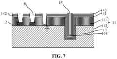
- FIG. 7 is a schematic structural view of a semiconductor structure obtained after an interconnection through hole is formed according to an embodiment of the disclosure.
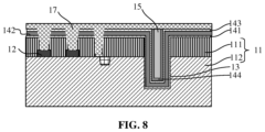
- FIG. 8 is a schematic sectional view of a semiconductor structure obtained after an interconnection material layer is formed according to an embodiment of the disclosure.
- FIG. 9 is a schematic sectional view of a semiconductor structure obtained after an interconnection structure is formed according to an embodiment of the disclosure.
- FIG. 10 is a schematic sectional view of a semiconductor structure obtained after a second dielectric layer is formed according to an embodiment of the disclosure.
- FIG. 11 is a schematic sectional view of a semiconductor structure obtained after trenches are formed in a second dielectric layer according to an embodiment of the disclosure.
- FIG. 12 is a schematic sectional view of a semiconductor structure obtained after a metal layer is formed according to an embodiment of the disclosure.
- FIG. 13 is a schematic sectional view of a semiconductor structure obtained after a substrate is thinned from a back side according to an embodiment of the disclosure.
- an element such as a layer, membrane or substrate is referred to as being “on” another membrane layer, it can be directly on the other membrane layer or there may be an intermediate membrane layer. Further, when a layer is referred to as being “under” another layer, it may be directly below, or there may be one or more intermediate layers. It is also understood that when a layer is referred to as being “between” two layers, it may be the only layer between the two layers, or there may be one or more intermediate layers.
- an embodiment of the disclosure provides a method for manufacturing a semiconductor structure. As shown in FIG. 1 , the method includes the following operations.
- a base 11 is provided.
- a TSV 13 is formed in the base 11 , a depth of the TSV 13 is less than a thickness of the base 11 .
- the liner layer includes a dielectric filler layer and the polish-stop layer that are sequentially stacked onto one another. As shown in FIG. 4 and FIG. 5 , the operations of forming the liner layer and the conductive layer 15 are as follows.
- a first polish-stop layer 141 is formed on an upper surface of the base 11 as well as the sidewall and bottom of the TSV 13 .
- a first dielectric filler layer 142 is formed on a surface of the first polish-stop layer 141 .
- a second polish-stop layer 143 is formed on a surface of the first dielectric filler layer 142 .
- a second dielectric filler layer 144 is formed on a surface of the second polish-stop layer 143 .
- the conductive layer 15 is formed on a surface of the second dielectric filler layer 144 , the conductive layer 15 covers an upper surface of the second dielectric filler layer 144 and entirely fill the TSV 13 .
- a portion of the conductive layer 15 located above the first polish-stop layer 141 , a portion of the second dielectric filler layer 144 located above the first polish-stop layer 141 , a portion of the second polish-stop layer 143 located above the first polish-stop layer 141 , and a portion of the first dielectric filler layer 142 located above first polish-stop layer 141 are removed.
- the first dielectric filler layer 142 and the second dielectric filler layer 144 may be silicon oxide layers.
- the first polish-stop layer 141 and the second polish-stop layer 143 may be silicon nitride layers or silicon carbon nitride layers.
- the conductive layer 15 may be a copper layer.
- FIG. 4 is a schematic structural sectional view of a semiconductor structure obtained after the liner layer is formed on the sidewall and bottom of the TSV 13 .
- FIG. 5 is a schematic sectional view of a semiconductor structure formed after the conductive layer 15 covers the upper surface of the second dielectric filler layer 144 and fills the TSV 13 .
- the conductive layer 15 may be formed on the surface of the second dielectric filler layer 144 by an electroplating process.
- the method may further include a operation of performing a planarization process, for example, chemical mechanical polishing, on surfaces of the above material layers.
- the polish-stop layer is added in a manufacturing process of the liner layer, so that a polishing progress may be determined by the polish-stop layer and the polishing rate may be adjusted in time in a subsequent polishing process, to prevent excessive polishing and the damage to the conductive layer 15 in the TSV 13 .
- the method further includes the following operations.
- an interconnection through hole 16 is formed, to expose the device units 12 .
- FIG. 6 is a schematic sectional view of a semiconductor structure formed after portions of the conductive layer 15 and the second dielectric filler layer 144 located above the second polish-stop layer 143 are removed.
- a photoresist layer with a photolithography pattern may be formed on the structure shown in FIG. 6 .
- a position of the photolithography pattern corresponds to the device units 12 in the first dielectric layer 111 .
- the second polish-stop layer 143 , the first dielectric filler layer 142 , the first polish-stop layer 141 , and the first dielectric layer 111 are etched in accordance with the photolithography pattern, to form the interconnection through hole 16 , as shown in FIG. 7 .
- an interconnection material layer 17 is formed in the interconnection through hole 16 and on an upper surface of the second polish-stop layer 143 .
- the interconnection material layer 17 may be at least one of a tungsten layer, an aluminum layer, a copper layer or a titanium nitride layer.
- FIG. 8 is a schematic sectional view of a semiconductor structure obtained after the interconnection material layer 17 is formed.
- the excessive interconnection material layer 17 needs to be removed.
- a polishing device is controlled to polish the portion of the interconnection material layer 17 located on the upper surface of the second polish-stop layer 143 , to remove this portion of the interconnection material layer 17 .
- a polishing resistance changes. For example, the polishing resistance significantly increases.
- the polishing device will be controlled to lower the polishing rate of the polishing device, then the polishing is continued to remove the portions of second polish-stop layer 143 and the first dielectric filler layer 142 located above the first polish-stop layer 141 .
- FIG. 9 is a schematic sectional view of a semiconductor structure obtained after the interconnection structure 18 is formed.
- the upper surface of the interconnection structure 18 is flush with the upper surface of the first polish-stop layer 141 .
- the interconnection structure 18 may be at least one of a tungsten layer, an aluminum layer, a copper layer or a titanium nitride layer.
- the forming the interconnection structure 18 further includes the following operations.
- a second dielectric layer 19 is formed on the upper surface of the first polish-stop layer 141 , the upper surface of the interconnection structure 18 , an upper surface of the liner layer, and an upper surface of the conductive layer 15 .
- FIG. 10 is a schematic sectional view of a semiconductor structure obtained after the second dielectric layer 19 is formed.
- a material of the second dielectric layer 19 may be the same as a material of the first dielectric filler layer 142 or the second dielectric filler layer 144 . That is, the second dielectric layer 19 may be a silicon oxide layer.
- trenches 20 are formed in the second dielectric layer 19 to expose the interconnection structure 18 and the conductive layer 15 respectively.
- FIG. 11 is a schematic sectional view of a semiconductor structure obtained after the trenches 20 are formed.
- the trenches 20 may be formed by a photolithography process.
- a metal layer 21 is formed in the trenches 20 .
- the metal layer 21 may be a copper layer.
- the metal layer 21 is first formed in the trenches 20 and on an upper surface of the second dielectric layer 19 by an electroplating process. A portion of the metal layer 21 on the upper surface of the second dielectric layer 19 is then removed by a chemical mechanical polishing process. A portion of the metal layer 21 in the trench 20 is retained, and a surface of the metal layer 21 is planarized, to enable the metal layer 21 in the trench 20 to be flush with the upper surface of the second dielectric layer 19 .
- the method further includes the following operations.
- the substrate 112 is thinned from a back side, until the bottom of the conductive layer 15 is exposed.
- the bottom of the conductive layer 15 is exposed, to enable different wafers to be connected by the conductive layer 15 in the TSV 13 , so as to implement a vertical interconnect stacking packaging.
- the thinning of the substrate 112 from the back side includes the following operations.
- the substrate 112 is thinned from a back side by polishing at a first polishing rate, until the polish-stop layer is exposed.
- the substrate 112 is continued to be thinned from the back side by polishing at a second polishing rate, until the bottom of the conductive layer 15 is exposed.
- the second polishing rate is less than the first polishing rate.
- back side of the substrate 112 is polished at the first polishing rate to reduce the thickness of the substrate.
- a signal indicating that the polishing resistance increases may be detected, and thus the first polish-stop layer 141 is identified.
- the polishing rate is lowered to the second polishing rate, then the polishing continues with the second polishing rate.
- a signal indicating that the polishing resistance increases may be detected again, and thus the second polish-stop layer 143 is identified.
- the polishing device may continue to perform polishing at the second polishing rate, until the bottom of the conductive layer 15 is exposed.
- the polishing device may also lower the polishing rate to a third polishing rate, to continue to perform the polishing at the third polishing rate, until the bottom of the conductive layer 15 is exposed.
- the third polishing rate is less than the second polishing rate, and the second polishing rate is less than the first polishing rate.
- the polish-stop layer is disposed in the liner layer of the TSV 13 , so that during the thinning of the substrate 112 from the back side, a polishing progress may be determined by detecting whether the polishing device comes into contact with the polish-stop layer, and the polishing rate may be adjusted in time, to avoid an phenomenon of excessive polishing, thereby preventing the conductive layer 15 from damage and avoiding affecting the electrical performance of the conductive layer 15 .
- a width of the interconnection through hole 16 is less than a width of the TSV 13 .
- the interconnection through hole 16 is located in the array region, a size of the interconnection through hole 16 usually corresponds to a size of the device unit 12 . Because the feature size of the device unit 12 keeps decreasing, the size of the interconnection through hole 16 also correspondingly decreases.
- the TSV 13 is located on a periphery of the array region, and there is no direct relation between the TSV and the size of the device unit 12 .
- the width of the TSV 13 may be appropriately increased, to enable the width of the TSV 13 to be greater than the width of the interconnection through hole 16 , so that a resistance of the conductive layer 15 in the TSV 13 can be reduced.
- the semiconductor structure includes: a base 11 , a TSV 13 located in the base 11 , a liner layer and a conductive layer 15 .
- a depth of the TSV 13 is less than a thickness of the base 11 .
- the liner layer is located at least on a sidewall and the bottom of the TSV 13 , and the liner layer includes a polish-stop layer.
- the conductive layer is located in the TSV 13 , and entirely fills the TSV 13 .
- the base 11 may include a substrate 112 and a first dielectric layer 111 on an upper surface of the substrate 112 .
- a plurality of device units 12 formed in the first dielectric layer 111 are arranged in an array.
- the device units 12 may be memory cells or may be a front trench isolation structure.
- the first dielectric layer 111 may be a silicon nitride layer or a silicon oxide layer.
- the TSV 13 passes through the first dielectric layer 111 , and partially extends into the substrate 112 .
- a part of the liner layer is located on the sidewall and bottom of the TSV 13 , and another part is located on an upper surface of the first dielectric layer 111 .
- the liner layer includes the polish-stop layer.
- the function of the polish-stop layer lies in that: during the polishing of a back surface (that is, a surface close to the bottom of the TSV 13 ) of the base 11 , a polishing rate may be adjusted in time according to a position of the polish-stop layer, to avoid excessive polishing, so that the precision is increased while the polishing efficiency is improved. For example, before the polishing device comes into contact with the polish-stop layer, the polishing may be performed at a relatively fast polishing rate.
- the polishing device When the polishing device comes into contact with the polish-stop layer, the polishing device receives a signal indicating that a polishing resistance changes. Then, a user may determine a current progress of the polishing, that is, the polishing device already approaches the bottom of the conductive layer 15 , and may appropriately decrease a polishing rate, to perform more accurate polishing.
- the liner layer includes a first polish-stop layer 141 , a first dielectric filler layer 142 , a second polish-stop layer 143 , and a second dielectric filler layer 144 that are sequentially stacked onto one another in a direction from the base 11 to the conductive layer 15 .
- the polishing device may more precisely adjust the polishing rate by means of the first polish-stop layer 141 and the second polish-stop layer 143 , thereby further improving the polishing efficiency and polishing precision.
- the substrate 112 may be thinned by polishing the back surface at a first polishing rate.
- a signal indicating an increase in the polishing resistance may be detected, and thus the first polish-stop layer 141 is identified.
- the polishing device is controlled to lower the polishing rate to a second polishing rate. Then, the polishing continues with the second polishing rate.
- the polishing device may continue to perform polishing at the second polishing rate, until the bottom of the conductive layer 15 is exposed.
- the polishing device may also lower the polishing rate to a third polishing rate, to continue to perform the polishing at the third polishing rate, until the bottom of the conductive layer 15 is exposed.
- the third polishing rate is less than the second polishing rate, and the second polishing rate is less than the first polishing rate.
- a plurality of polish-stop layers are disposed.
- the user may perform polishing at a relatively fast speed with confidence before the polishing device comes into contact with the next polish-stop layer without worrying about the excessive polishing.
- the polishing rate is adjusted only after the polishing device comes into contact with the polish-stop layer, to perform more cautious and precise polishing, so that the polishing efficiency is improved while the polishing precision is ensured.
- the first dielectric filler layer 142 and the second dielectric filler layer 144 both include a silicon oxide layer.
- the first polish-stop layer 141 and the second polish-stop layer 143 both include a silicon nitride layer or a silicon carbon nitride layer.
- the polish-stop layer is a silicon nitride (Si 3 N 4 ) layer.
- Silicon nitride is a structural ceramic material, has a high hardness and wear resistance, and is very suitable for use as a mask stop layer.
- the polishing device may detect an increase in the polishing resistance, thereby prompting the user to lower the polishing rate, to avoid the excessive polishing.
- the base 11 includes an array region and a peripheral region located on a periphery of the array region.
- the TSV 13 is located in the peripheral region.
- the base 11 includes the substrate 112 and the first dielectric layer 111 located on the upper surface of the substrate 112 .
- the plurality of device units 12 arranged in an array are formed in the first dielectric layer 111 in the array region.
- the first polish-stop layer 141 extends to the upper surface of the first dielectric layer 111 .
- the semiconductor structure further includes an interconnection structure 18 , a second dielectric layer 19 and a metal layer 21 .
- the bottom of the interconnection structure 18 is in contact with the device units 12 , an upper surface of the interconnection structure 18 is flush with an upper surface of the first polish-stop layer 141 .
- the second dielectric layer 19 is located on the upper surface of the first polish-stop layer 141 , an upper surface of the liner layer, and an upper surface of the conductive layer 15 .
- the metal layer 21 is located in the second dielectric layer 19 , and in contact with the device units 12 and the conductive layer 15 .
- the metal layer 21 includes a plurality of metal structures, which are in contact with the interconnection structure 18 and the conductive layer 15 respectively.
- the metal layer 21 includes a copper metal structure.
- the interconnection structure 18 includes at least one of a tungsten layer, an aluminum layer, a copper layer or a titanium nitride layer.
- the device units 12 include memory cells.
- the first dielectric layer 111 includes a silicon nitride layer or a silicon oxide layer.
- the second dielectric layer 19 includes a silicon oxide layer.
- the semiconductor structure includes: a base 11 , a TSV 13 located in the base 11 , a liner layer at least located on a sidewall of the TSV 13 and a conductive layer 15 .
- a depth of the TSV 13 is equal to a thickness of the base 11 .
- the liner layer includes a polish-stop layer.
- the conductive layer is located in the TSV 13 , and entirely fills the TSV 13 .
- the polish-stop layer is formed in the liner layer of the TSV, so that a polishing progress may be determined by the polish-stop layer and a polishing rate may be adjusted in time in a process of polishing a back surface of the base to penetrate the TSV, to prevent damage to the conductive layer in the TSV due to the excessive polishing.
Landscapes
- Internal Circuitry In Semiconductor Integrated Circuit Devices (AREA)
Abstract
Description
Claims (3)
Applications Claiming Priority (3)
| Application Number | Priority Date | Filing Date | Title |
|---|---|---|---|
| CN202110500614.6A CN115312449A (en) | 2021-05-08 | 2021-05-08 | Semiconductor structure and preparation method thereof |
| CN202110500614.6 | 2021-05-08 | ||
| PCT/CN2021/120247 WO2022237044A1 (en) | 2021-05-08 | 2021-09-24 | Semiconductor structure and preparation method therefor |
Related Parent Applications (1)
| Application Number | Title | Priority Date | Filing Date |
|---|---|---|---|
| PCT/CN2021/120247 Continuation WO2022237044A1 (en) | 2021-05-08 | 2021-09-24 | Semiconductor structure and preparation method therefor |
Publications (2)
| Publication Number | Publication Date |
|---|---|
| US20220359291A1 US20220359291A1 (en) | 2022-11-10 |
| US12243779B2 true US12243779B2 (en) | 2025-03-04 |
Family
ID=83900662
Family Applications (1)
| Application Number | Title | Priority Date | Filing Date |
|---|---|---|---|
| US17/689,000 Active 2042-10-26 US12243779B2 (en) | 2021-05-08 | 2022-03-08 | Semiconductor structure and method for manufacturing semiconductor structure |
Country Status (2)
| Country | Link |
|---|---|
| US (1) | US12243779B2 (en) |
| EP (1) | EP4117029B1 (en) |
Citations (10)
| Publication number | Priority date | Publication date | Assignee | Title |
|---|---|---|---|---|
| US20110316166A1 (en) | 2010-06-28 | 2011-12-29 | Globalfoundries Singapore Pte. Ltd. | Integrated circuit system with via and method of manufacture thereof |
| US20120142190A1 (en) | 2010-12-07 | 2012-06-07 | United Microelectronics Corp. | Method for manufacturing through-silicon via |
| US20120248581A1 (en) | 2011-03-31 | 2012-10-04 | Elpida Memory, Inc. | Semiconductor device and manufacturing method thereof |
| US20120261827A1 (en) * | 2011-04-13 | 2012-10-18 | Taiwan Semiconductor Manufacturing Company, Ltd. | Through-silicon vias for semicondcutor substrate and method of manufacture |
| TW201342526A (en) | 2012-04-13 | 2013-10-16 | 聯華電子股份有限公司 | Piercing conductor structure and its preparation method |
| US20140070426A1 (en) | 2012-09-12 | 2014-03-13 | Jae-hwa Park | Integrated circuit devices including a via structure and methods of fabricating integrated circuit devices including a via structure |
| US20140264911A1 (en) * | 2013-03-15 | 2014-09-18 | Globalfoundries Singapore Pte. Ltd. | Through silicon vias |
| CN103545275B (en) | 2012-07-12 | 2016-02-17 | 中芯国际集成电路制造(上海)有限公司 | Silicon through hole encapsulating structure and formation method |
| US20170256476A1 (en) * | 2016-03-03 | 2017-09-07 | Samsung Electronics Co., Ltd. | Semiconductor devices having through electrodes and methods for fabricating the same |
| CN107591387A (en) | 2016-07-06 | 2018-01-16 | 三星电子株式会社 | Semiconductor package part and the method for forming the semiconductor package part |
-
2021
- 2021-09-24 EP EP21870475.7A patent/EP4117029B1/en active Active
-
2022
- 2022-03-08 US US17/689,000 patent/US12243779B2/en active Active
Patent Citations (19)
| Publication number | Priority date | Publication date | Assignee | Title |
|---|---|---|---|---|
| US20110316166A1 (en) | 2010-06-28 | 2011-12-29 | Globalfoundries Singapore Pte. Ltd. | Integrated circuit system with via and method of manufacture thereof |
| US20120142190A1 (en) | 2010-12-07 | 2012-06-07 | United Microelectronics Corp. | Method for manufacturing through-silicon via |
| US20120248581A1 (en) | 2011-03-31 | 2012-10-04 | Elpida Memory, Inc. | Semiconductor device and manufacturing method thereof |
| US20120261827A1 (en) * | 2011-04-13 | 2012-10-18 | Taiwan Semiconductor Manufacturing Company, Ltd. | Through-silicon vias for semicondcutor substrate and method of manufacture |
| TW201342526A (en) | 2012-04-13 | 2013-10-16 | 聯華電子股份有限公司 | Piercing conductor structure and its preparation method |
| CN103545275B (en) | 2012-07-12 | 2016-02-17 | 中芯国际集成电路制造(上海)有限公司 | Silicon through hole encapsulating structure and formation method |
| US9337125B2 (en) | 2012-09-12 | 2016-05-10 | Samsung Electronics Co., Ltd. | Integrated circuit devices including a via structure and methods of fabricating integrated circuit devices including a via structure |
| CN103681573A (en) | 2012-09-12 | 2014-03-26 | 三星电子株式会社 | Integrated circuit devices including a via structure and methods of fabricating integrated circuit devices including a via structure |
| US20140070426A1 (en) | 2012-09-12 | 2014-03-13 | Jae-hwa Park | Integrated circuit devices including a via structure and methods of fabricating integrated circuit devices including a via structure |
| US9437547B2 (en) | 2013-03-15 | 2016-09-06 | Globalfoundries Singapore Pte. Ltd. | Through silicon vias |
| US9287197B2 (en) | 2013-03-15 | 2016-03-15 | Globalfoundries Singapore Pte. Ltd. | Through silicon vias |
| US20160190066A1 (en) | 2013-03-15 | 2016-06-30 | Globalfoundries Singapore Pte. Ltd. | Through silicon vias |
| US20140264911A1 (en) * | 2013-03-15 | 2014-09-18 | Globalfoundries Singapore Pte. Ltd. | Through silicon vias |
| US20170256476A1 (en) * | 2016-03-03 | 2017-09-07 | Samsung Electronics Co., Ltd. | Semiconductor devices having through electrodes and methods for fabricating the same |
| US10340204B2 (en) | 2016-03-03 | 2019-07-02 | Samsung Electronics Co., Ltd. | Semiconductor devices having through electrodes and methods for fabricating the same |
| US20190279920A1 (en) | 2016-03-03 | 2019-09-12 | Samsung Electronics Co., Ltd. | Semiconductor devices having through electrodes and methods for fabricating the same |
| US10950523B2 (en) | 2016-03-03 | 2021-03-16 | Samsung Electronics Co., Ltd. | Semiconductor devices having through electrodes and methods for fabricating the same |
| US20210143086A1 (en) | 2016-03-03 | 2021-05-13 | Samsung Electronics Co., Ltd. | Semiconductor devices having through electrodes and methods for fabricating the same |
| CN107591387A (en) | 2016-07-06 | 2018-01-16 | 三星电子株式会社 | Semiconductor package part and the method for forming the semiconductor package part |
Non-Patent Citations (2)
| Title |
|---|
| International Search Report in the international application No. PCT/CN2021/120247, mailed on Dec. 27, 2021, 2 pgs. |
| Supplementary European Search Report in the European application No. 21870475.7, mailed on Dec. 19, 2022, 8 pgs. |
Also Published As
| Publication number | Publication date |
|---|---|
| EP4117029A4 (en) | 2023-01-18 |
| US20220359291A1 (en) | 2022-11-10 |
| EP4117029A1 (en) | 2023-01-11 |
| EP4117029B1 (en) | 2024-01-24 |
Similar Documents
| Publication | Publication Date | Title |
|---|---|---|
| KR20230125309A (en) | Structures having through-substrate vias and methods for forming the same | |
| KR100383504B1 (en) | Semiconductor device and method of producing the same | |
| US20140035109A1 (en) | Method and structure of forming backside through silicon via connections | |
| US11342221B2 (en) | Semiconductor device | |
| JP2003197855A (en) | Semiconductor device and method of manufacturing the same | |
| US20070254453A1 (en) | Method of Improving a Shallow Trench Isolation Gapfill Process | |
| US20110260297A1 (en) | Through-substrate via and fabrication method thereof | |
| US9153492B2 (en) | Semiconductor device and method for fabricating the same | |
| US20210050221A1 (en) | Method of fabricating a semiconductor device | |
| JP2007043154A (en) | Method of manufacturing a semiconductor structure having wafer through contacts and corresponding semiconductor structure | |
| JP4456027B2 (en) | Method for manufacturing through conductor | |
| JP3645129B2 (en) | Manufacturing method of semiconductor device | |
| JP4064732B2 (en) | Semiconductor device | |
| US20150147878A1 (en) | Semiconductor device and method for manufacturing the same | |
| US12243779B2 (en) | Semiconductor structure and method for manufacturing semiconductor structure | |
| US7094653B2 (en) | Method for forming STI structures with controlled step height | |
| CN112185969B (en) | Three-dimensional memory structure and preparation method thereof | |
| US6977216B2 (en) | Method for forming metal wire in semiconductor device | |
| CN115312449A (en) | Semiconductor structure and preparation method thereof | |
| US6458708B1 (en) | Method for forming metal wiring in semiconductor device | |
| KR100390838B1 (en) | Method for forming landing plug contact in semiconductor device | |
| CN108520863B (en) | Method for manufacturing shallow trench insulation structure | |
| CN118824940B (en) | Semiconductor structure manufacturing method, semiconductor structure, and semiconductor bonding structure | |
| KR100875350B1 (en) | STI Formation Method to Prevent Divot | |
| CN120878558A (en) | Semiconductor structure, forming method thereof and semiconductor stacking structure |
Legal Events
| Date | Code | Title | Description |
|---|---|---|---|
| FEPP | Fee payment procedure |
Free format text: ENTITY STATUS SET TO UNDISCOUNTED (ORIGINAL EVENT CODE: BIG.); ENTITY STATUS OF PATENT OWNER: LARGE ENTITY |
|
| STPP | Information on status: patent application and granting procedure in general |
Free format text: DOCKETED NEW CASE - READY FOR EXAMINATION |
|
| AS | Assignment |
Owner name: CHANGXIN MEMORY TECHNOLOGIES, INC., CHINA Free format text: ASSIGNMENT OF ASSIGNORS INTEREST;ASSIGNORS:WU, SHUANGSHUANG;LEE, TZUNG-HAN;SIGNING DATES FROM 20211019 TO 20211022;REEL/FRAME:060008/0001 |
|
| STPP | Information on status: patent application and granting procedure in general |
Free format text: NON FINAL ACTION MAILED |
|
| STPP | Information on status: patent application and granting procedure in general |
Free format text: RESPONSE TO NON-FINAL OFFICE ACTION ENTERED AND FORWARDED TO EXAMINER |
|
| STPP | Information on status: patent application and granting procedure in general |
Free format text: NOTICE OF ALLOWANCE MAILED -- APPLICATION RECEIVED IN OFFICE OF PUBLICATIONS |
|
| STPP | Information on status: patent application and granting procedure in general |
Free format text: PUBLICATIONS -- ISSUE FEE PAYMENT VERIFIED |
|
| STCF | Information on status: patent grant |
Free format text: PATENTED CASE |