US12238978B2 - Display device including shock absorbing layer - Google Patents
Display device including shock absorbing layer Download PDFInfo
- Publication number
- US12238978B2 US12238978B2 US17/521,476 US202117521476A US12238978B2 US 12238978 B2 US12238978 B2 US 12238978B2 US 202117521476 A US202117521476 A US 202117521476A US 12238978 B2 US12238978 B2 US 12238978B2
- Authority
- US
- United States
- Prior art keywords
- layer
- insulating layer
- interlayer insulating
- display device
- thickness
- Prior art date
- Legal status (The legal status is an assumption and is not a legal conclusion. Google has not performed a legal analysis and makes no representation as to the accuracy of the status listed.)
- Active, expires
Links
Images


Classifications
-
- H—ELECTRICITY
- H10—SEMICONDUCTOR DEVICES; ELECTRIC SOLID-STATE DEVICES NOT OTHERWISE PROVIDED FOR
- H10K—ORGANIC ELECTRIC SOLID-STATE DEVICES
- H10K59/00—Integrated devices, or assemblies of multiple devices, comprising at least one organic light-emitting element covered by group H10K50/00
- H10K59/10—OLED displays
- H10K59/12—Active-matrix OLED [AMOLED] displays
- H10K59/124—Insulating layers formed between TFT elements and OLED elements
-
- H—ELECTRICITY
- H10—SEMICONDUCTOR DEVICES; ELECTRIC SOLID-STATE DEVICES NOT OTHERWISE PROVIDED FOR
- H10K—ORGANIC ELECTRIC SOLID-STATE DEVICES
- H10K50/00—Organic light-emitting devices
- H10K50/80—Constructional details
- H10K50/84—Passivation; Containers; Encapsulations
- H10K50/844—Encapsulations
-
- H—ELECTRICITY
- H10—SEMICONDUCTOR DEVICES; ELECTRIC SOLID-STATE DEVICES NOT OTHERWISE PROVIDED FOR
- H10K—ORGANIC ELECTRIC SOLID-STATE DEVICES
- H10K59/00—Integrated devices, or assemblies of multiple devices, comprising at least one organic light-emitting element covered by group H10K50/00
- H10K59/40—OLEDs integrated with touch screens
-
- G—PHYSICS
- G06—COMPUTING OR CALCULATING; COUNTING
- G06F—ELECTRIC DIGITAL DATA PROCESSING
- G06F3/00—Input arrangements for transferring data to be processed into a form capable of being handled by the computer; Output arrangements for transferring data from processing unit to output unit, e.g. interface arrangements
- G06F3/01—Input arrangements or combined input and output arrangements for interaction between user and computer
- G06F3/03—Arrangements for converting the position or the displacement of a member into a coded form
- G06F3/041—Digitisers, e.g. for touch screens or touch pads, characterised by the transducing means
- G06F3/0412—Digitisers structurally integrated in a display
-
- H—ELECTRICITY
- H10—SEMICONDUCTOR DEVICES; ELECTRIC SOLID-STATE DEVICES NOT OTHERWISE PROVIDED FOR
- H10K—ORGANIC ELECTRIC SOLID-STATE DEVICES
- H10K2102/00—Constructional details relating to the organic devices covered by this subclass
- H10K2102/301—Details of OLEDs
- H10K2102/351—Thickness
-
- H—ELECTRICITY
- H10—SEMICONDUCTOR DEVICES; ELECTRIC SOLID-STATE DEVICES NOT OTHERWISE PROVIDED FOR
- H10K—ORGANIC ELECTRIC SOLID-STATE DEVICES
- H10K50/00—Organic light-emitting devices
- H10K50/80—Constructional details
- H10K50/868—Arrangements for polarized light emission
-
- H—ELECTRICITY
- H10—SEMICONDUCTOR DEVICES; ELECTRIC SOLID-STATE DEVICES NOT OTHERWISE PROVIDED FOR
- H10K—ORGANIC ELECTRIC SOLID-STATE DEVICES
- H10K59/00—Integrated devices, or assemblies of multiple devices, comprising at least one organic light-emitting element covered by group H10K50/00
- H10K59/10—OLED displays
- H10K59/12—Active-matrix OLED [AMOLED] displays
- H10K59/121—Active-matrix OLED [AMOLED] displays characterised by the geometry or disposition of pixel elements
- H10K59/1213—Active-matrix OLED [AMOLED] displays characterised by the geometry or disposition of pixel elements the pixel elements being TFTs
-
- H—ELECTRICITY
- H10—SEMICONDUCTOR DEVICES; ELECTRIC SOLID-STATE DEVICES NOT OTHERWISE PROVIDED FOR
- H10K—ORGANIC ELECTRIC SOLID-STATE DEVICES
- H10K59/00—Integrated devices, or assemblies of multiple devices, comprising at least one organic light-emitting element covered by group H10K50/00
- H10K59/10—OLED displays
- H10K59/12—Active-matrix OLED [AMOLED] displays
- H10K59/121—Active-matrix OLED [AMOLED] displays characterised by the geometry or disposition of pixel elements
- H10K59/1216—Active-matrix OLED [AMOLED] displays characterised by the geometry or disposition of pixel elements the pixel elements being capacitors
-
- H—ELECTRICITY
- H10—SEMICONDUCTOR DEVICES; ELECTRIC SOLID-STATE DEVICES NOT OTHERWISE PROVIDED FOR
- H10K—ORGANIC ELECTRIC SOLID-STATE DEVICES
- H10K59/00—Integrated devices, or assemblies of multiple devices, comprising at least one organic light-emitting element covered by group H10K50/00
- H10K59/10—OLED displays
- H10K59/12—Active-matrix OLED [AMOLED] displays
- H10K59/122—Pixel-defining structures or layers, e.g. banks
-
- H—ELECTRICITY
- H10—SEMICONDUCTOR DEVICES; ELECTRIC SOLID-STATE DEVICES NOT OTHERWISE PROVIDED FOR
- H10K—ORGANIC ELECTRIC SOLID-STATE DEVICES
- H10K59/00—Integrated devices, or assemblies of multiple devices, comprising at least one organic light-emitting element covered by group H10K50/00
- H10K59/10—OLED displays
- H10K59/12—Active-matrix OLED [AMOLED] displays
- H10K59/123—Connection of the pixel electrodes to the thin film transistors [TFT]
-
- H—ELECTRICITY
- H10—SEMICONDUCTOR DEVICES; ELECTRIC SOLID-STATE DEVICES NOT OTHERWISE PROVIDED FOR
- H10K—ORGANIC ELECTRIC SOLID-STATE DEVICES
- H10K59/00—Integrated devices, or assemblies of multiple devices, comprising at least one organic light-emitting element covered by group H10K50/00
- H10K59/10—OLED displays
- H10K59/12—Active-matrix OLED [AMOLED] displays
- H10K59/126—Shielding, e.g. light-blocking means over the TFTs
-
- H—ELECTRICITY
- H10—SEMICONDUCTOR DEVICES; ELECTRIC SOLID-STATE DEVICES NOT OTHERWISE PROVIDED FOR
- H10K—ORGANIC ELECTRIC SOLID-STATE DEVICES
- H10K59/00—Integrated devices, or assemblies of multiple devices, comprising at least one organic light-emitting element covered by group H10K50/00
- H10K59/10—OLED displays
- H10K59/12—Active-matrix OLED [AMOLED] displays
- H10K59/131—Interconnections, e.g. wiring lines or terminals
-
- H—ELECTRICITY
- H10—SEMICONDUCTOR DEVICES; ELECTRIC SOLID-STATE DEVICES NOT OTHERWISE PROVIDED FOR
- H10K—ORGANIC ELECTRIC SOLID-STATE DEVICES
- H10K59/00—Integrated devices, or assemblies of multiple devices, comprising at least one organic light-emitting element covered by group H10K50/00
- H10K59/30—Devices specially adapted for multicolour light emission
- H10K59/35—Devices specially adapted for multicolour light emission comprising red-green-blue [RGB] subpixels
- H10K59/352—Devices specially adapted for multicolour light emission comprising red-green-blue [RGB] subpixels the areas of the RGB subpixels being different
-
- H—ELECTRICITY
- H10—SEMICONDUCTOR DEVICES; ELECTRIC SOLID-STATE DEVICES NOT OTHERWISE PROVIDED FOR
- H10K—ORGANIC ELECTRIC SOLID-STATE DEVICES
- H10K59/00—Integrated devices, or assemblies of multiple devices, comprising at least one organic light-emitting element covered by group H10K50/00
- H10K59/30—Devices specially adapted for multicolour light emission
- H10K59/38—Devices specially adapted for multicolour light emission comprising colour filters or colour changing media [CCM]
-
- H—ELECTRICITY
- H10—SEMICONDUCTOR DEVICES; ELECTRIC SOLID-STATE DEVICES NOT OTHERWISE PROVIDED FOR
- H10K—ORGANIC ELECTRIC SOLID-STATE DEVICES
- H10K59/00—Integrated devices, or assemblies of multiple devices, comprising at least one organic light-emitting element covered by group H10K50/00
- H10K59/80—Constructional details
- H10K59/87—Passivation; Containers; Encapsulations
- H10K59/873—Encapsulations
- H10K59/8731—Encapsulations multilayered coatings having a repetitive structure, e.g. having multiple organic-inorganic bilayers
Definitions
- One or more embodiments relate to display devices.
- Mobility-based electronic devices are widely used. As mobile electronic devices, in addition to small electronic devices such as mobile phones, tablet PCs have been widely used in recent years.
- Such mobile electronic devices include display devices to support various functions and provide visual information such as images or video to a user.
- display devices to support various functions and provide visual information such as images or video to a user.
- the proportion of display devices in electronic devices is gradually increasing, and a structure that can be bent to have a certain angle with respect to a flat state is being developed.
- some layers of the display device may be broken or damaged.
- some inner layers are broken or damaged such that some pixels of the display device do not work and dark dots may form.
- the above problem occurs in display devices that are freely deformable.
- One or more embodiments relate to display devices capable of implementing clear images even after external impacts are applied thereto.
- a display device includes a substrate, a semiconductor layer on the substrate, an interlayer insulating layer on the semiconductor layer, a source electrode or a drain electrode on the interlayer insulating layer, and connected to the semiconductor layer, an organic light-emitting diode connected to the source electrode or the drain electrode, and a thin film encapsulation layer on the organic light-emitting diode, wherein, a neutral plane corresponding to an impact applied to the thin film encapsulation layer is inside or below the interlayer insulating layer.
- a distance from a bottom of the substrate to a bottom of the interlayer insulating layer may be greater than a distance from an upper surface of the interlayer insulating layer to an upper surface of the thin film encapsulation layer.
- the thin film encapsulation layer may include an organic encapsulation layer, wherein a thickness of the organic encapsulation layer is between about 0.16 times and about 0.26 times a distance from a bottom of the substrate to an upper surface of the thin film encapsulation layer.
- the interlayer insulating layer may include a first interlayer insulating layer, and a second interlayer insulating layer on the first interlayer insulating layer.
- a thickness of the first interlayer insulating layer may be greater than a thickness of the second interlayer insulating layer.
- the second interlayer insulating layer may have a structure in which an inorganic material and an organic material are sequentially stacked.
- the first interlayer insulating layer may include silicon oxide.
- the display device may further include a shock absorbing layer on the interlayer insulating layer.
- the shock absorbing layer may include an organic material.
- the display device may further include an input detection member on the thin film encapsulation layer.
- a display device includes a substrate, a semiconductor layer on the substrate, an interlayer insulating layer on the semiconductor layer, a source electrode or a drain electrode on the interlayer insulating layer, and connected to the semiconductor layer, an organic light-emitting diode connected to the source electrode or the drain electrode, and a thin film encapsulation layer on the organic light-emitting diode, wherein a thickness of the substrate is between about 0.5 times and about 0.76 times a distance from a lower surface of the substrate to an upper surface of the thin film encapsulation layer.
- the thin film encapsulation layer may include an organic encapsulation layer, wherein a thickness of the organic encapsulation layer is between about 0.16 times and about 0.26 times a distance from a bottom of the substrate to an upper surface of the thin film encapsulation layer.
- the interlayer insulating layer may include a first interlayer insulating layer, and a second interlayer insulating layer on the first interlayer insulating layer.
- a thickness of the first interlayer insulating layer may be greater than a thickness of the second interlayer insulating layer.
- the second interlayer insulating layer may have a structure in which an inorganic material and an organic material are sequentially stacked.
- the first interlayer insulating layer may include silicon oxide.
- the display device may further include a shock absorbing layer on the interlayer insulating layer.
- the shock absorbing layer may include an organic material.
- the display device may further include an input detection member on the thin film encapsulation layer.
- a display device includes a substrate, a semiconductor layer on the substrate, an interlayer insulating layer on the semiconductor layer, a source electrode or a drain electrode on the interlayer insulating layer, and connected to the semiconductor layer, an organic light-emitting diode connected to the source electrode or the drain electrode, and a thin film encapsulation layer on the organic light-emitting diode, wherein a compressive force corresponding to an impact is applied to the thin film encapsulation layer is generated in the interlayer insulating layer.
- the interlayer insulating layer may include a first interlayer insulating layer, and a second interlayer insulating layer on the first interlayer insulating layer.
- the second interlayer insulating layer may have a structure in which an inorganic material and an organic material are sequentially stacked.
- FIG. 1 is a schematic plan view of a display device according to some embodiments.
- FIG. 2 is a cross-sectional view of a part of the display of FIG. 1 ;
- FIG. 3 is a schematic plan view of the display device of FIG. 1 ;
- FIG. 4 is a cross-sectional view of a part of the display device of FIG. 1 ;
- FIG. 5 is a cross-sectional view of part of a display device according to some embodiments.
- FIG. 6 is a cross-sectional view of part of a display device according to some embodiments.
- FIG. 7 is a cross-sectional view of part of a display device according to some embodiments.
- FIG. 8 is a cross-sectional view of part of a display device according to some embodiments.
- FIG. 9 is a cross-sectional view of part of a display device according to some embodiments.
- FIG. 10 is a cross-sectional view of part of a display device according to some embodiments.
- FIG. 11 is a cross-sectional view of part of a display device according to some embodiments.
- an implanted region illustrated as a rectangle will, typically, have rounded or curved features and/or a gradient of implant concentration at its edges rather than a binary change from implanted to non-implanted region.
- a buried region formed by implantation may result in some implantation in the region between the buried region and the surface through which the implantation takes place.
- spatially relative terms such as “beneath,” “below,” “lower,” “under,” “above,” “upper,” and the like, may be used herein for ease of explanation to describe one element or feature's relationship to another element(s) or feature(s) as illustrated in the figures. It will be understood that the spatially relative terms are intended to encompass different orientations of the device in use or in operation, in addition to the orientation depicted in the figures. For example, if the device in the figures is turned over, elements described as “below” or “beneath” or “under” other elements or features would then be oriented “above” the other elements or features. Thus, the example terms “below” and “under” can encompass both an orientation of above and below.
- the device may be otherwise oriented (e.g., rotated 90 degrees or at other orientations) and the spatially relative descriptors used herein should be interpreted accordingly.
- first part is described as being arranged “on” a second part, this indicates that the first part is arranged at an upper side or a lower side of the second part without the limitation to the upper side thereof on the basis of the gravity direction.
- the phrase “on a plane,” or “plan view,” means viewing a target portion from the top
- the phrase “on a cross-section” means viewing a cross-section formed by vertically cutting a target portion from the side.
- a layer, region, or component when a layer, region, or component is referred to as being “electrically connected” or “electrically coupled” to another layer, region, or component, it can be directly electrically connected or coupled to the other layer, region, and/or component or intervening layers, regions, or components may be present.
- “directly connected/directly coupled,” or “directly on,” refers to one component directly connecting or coupling another component, or being on another component, without an intermediate component.
- other expressions describing relationships between components such as “between,” “immediately between” or “adjacent to” and “directly adjacent to” may be construed similarly.
- an element or layer when referred to as being “between” two elements or layers, it can be the only element or layer between the two elements or layers, or one or more intervening elements or layers may also be present.
- the x-axis, the y-axis, and/or the z-axis are not limited to three axes of a rectangular coordinate system, and may be interpreted in a broader sense.
- the x-axis, the y-axis, and the z-axis may be perpendicular to one another, or may represent different directions that are not perpendicular to one another. The same applies for first, second, and/or third directions.
- a thickness is measured in the z-axis direction of the drawing, and it may mean a distance from one side of one layer to one side of another layer at any point.
- the thickness of each layer may also be interpreted as the thickness of an arithmetic mean on the entire surface of each layer in addition to the value measured at any point.
- a specific process order may be performed differently from the described order.
- two consecutively described processes may be performed substantially at the same time or performed in an order opposite to the described order.
- FIG. 1 is a schematic plan view of a display device 10 according to some embodiments.
- FIG. 2 is a cross-sectional view of a part of the display device 10 , taken along the line A-A′ of FIG. 1 .
- FIG. 3 is a schematic plan view of the display device 10 of FIG. 1 .
- the display device 10 may include a display area DA and a non-display area NDA.
- the display area DA is where pixels P are arranged.
- the display area DA may provide an image by using light emitted from the pixels P.
- the pixels P may be connected to respective signal lines, such as a scan line SL extending in an x-axis direction and a data line DL extending in a y-axis direction.
- the pixel P may be connected to power lines configured to deliver DC signals, such as a driving power line, a common power line, and the like.
- the display area DA may be covered by a thin film encapsulation layer 400 overlapping a substrate 100 .
- the pixel P may include a pixel circuit electrically connected to the above-described signal lines and power line, and a display element, for example, an organic light-emitting diode (OLED), in the pixel circuit.
- the pixel P may emit, for example, red, green, blue, or white light, through the OLED.
- the non-display area NDA may include a first scan driver 11 , a second scan driver 12 , a terminal part 20 , a driving voltage supply line 30 , a common voltage supply line 40 , and a wiring layer 50 .
- the non-display area NDA is where no pixel is arranged.
- the first scan driver 11 and the second scan driver 12 may be arranged in the non-display area NDA.
- the first scan driver 11 and the second scan driver 12 may be apart from each other with the display area DA therebetween.
- the first scan driver 11 and/or the second scan driver 12 may generate and deliver scan signals to the pixels P through the scan lines SL.
- FIG. 1 illustrates a case in which two scan drivers are arranged, the disclosure is not limited thereto. In other embodiments, one scan driver may be arranged at one side of the display area DA.
- the terminal part 20 may be arranged at one end portion of the non-display area NDA, and may include terminals 21 , 22 , 23 , and 24 .
- the terminal part 20 may be exposed due to not being covered by an insulating layer, and may be connected to a driver IC 13 .
- the driver IC 13 may include a data driver.
- the driving voltage supply line 30 may provide a driving voltage to the pixels P.
- the driving voltage supply line 30 may be arranged in the non-display area NDA to be adjacent to one side of the display area DA.
- the common voltage supply line 40 may provide a common voltage to the pixels P.
- the common voltage may be applied to a cathode electrode of the OLED, and the common voltage supply line 40 may be arranged in the non-display area NDA to partially surround the display area DA.
- a first wiring 51 , a second wiring 52 , a third wiring 53 , and a fourth wiring 54 may be arranged between one end portion of the display area DA and the terminal part 20 , and may extend in a y-axis direction.
- the first wiring 51 electrically connects the signal lines of the display area DA to the terminal part 20
- the second wiring 52 electrically connects the driving voltage supply line 30 to the terminal part 20 .
- the third wiring 53 electrically connects each of the first scan driver 11 and the second scan driver 12 to the terminal part 20
- the fourth wiring 54 electrically connects the common voltage supply line 40 to the terminal part 20 .
- a display layer 200 is arranged on the substrate 100 .
- the display layer 200 may include a plurality of pixels. As each pixel may include a display element and a pixel circuit for an operation of the display element, the display layer 200 may include a plurality of display elements and pixel circuits connected to the respective display elements.
- the display layer 200 may be shielded by the thin film encapsulation layer 400 .
- the thin film encapsulation layer 400 may include at least one organic encapsulation layer and at least one inorganic encapsulation layer. At least one organic encapsulation layer and at least one inorganic encapsulation layer may be alternately stacked.
- An input detection member TSL and an optical functional member OFL may be arranged on the thin film encapsulation layer 400 .
- the input detection member TSL may include a touch electrode TD of various patterns for a touch screen function.
- the touch electrode TD may include first touch electrodes TD 1 connected to each other in a first direction (y-axis direction), and second touch electrodes TD 2 connected to each other in a second direction (x-axis direction) crossing the first direction.
- the touch electrode TD may include a transparent electrode material to transmit light from a light-emitting area of pixels arranged below the input detection member TSL.
- the touch electrode TD may be provided in a mesh shape to transmit light from the light-emitting area of pixels.
- the touch electrode TD is not limited to a transparent electrode material.
- the touch electrode TD may be a single film or a multilayer film including a conductive material including aluminum (Al), copper (Cu), and/or titanium (Ti), and the like.
- the touch electrode TD may be connected to a touch wiring TL configured to deliver a sensed signal to the touch electrode TD, and the touch wiring TL may extend from an upper surface of the thin film encapsulation layer 400 toward the non-display area NDA at one surface of the thin film encapsulation layer 400 .
- the touch wiring TL may be connected to the touch electrode TD of the input detection member TSL of the display area DA, and may extend from an upper portion of the thin film encapsulation layer 400 .
- the touch wiring TL may be connected to a touch terminal 25 of the terminal part 20 to exchange electrical signals with the input detection member TSL.
- the optical functional member OFL may reduce reflectivity of light (external light) incident on the display device 10 from the outside, and/or improve color purity of light emitted from the display device 10 .
- the optical functional member OFL may include a retarder and a polarizer.
- the retarder may be of a film type or a liquid crystal coating type, and may include a ⁇ /2 retarder and/or a ⁇ /4 retarder.
- the polarizer may also be of a film type or a liquid crystal coating type.
- the film type may include a stretchable synthetic resin film, and the liquid crystal coating type may include liquid crystals arranged in a certain array.
- the optical functional member OFL may include a black matrix and color filters.
- the color filters may be arranged considering the color of light emitted from each of the pixels of the display device 10 .
- Each of the color filters may include red, green, or blue pigment or dye.
- each of the color filters may further include quantum dots in addition to the above-described pigment or dye.
- some of the color filters may not include the above-described pigment or dye, and may include scattering particles such as titanium oxide.
- the optical functional member OFL may include a destructive interference structure.
- the destructive interference structure may include two reflective layers. Reflected light reflected from one of the two reflective layers may undergo destructive interference with reflected light reflected from the other of the two reflective layers, and thus reflectivity of external light may be reduced.
- FIG. 4 is a cross-sectional view of a part of the display device 10 of FIG. 1 .
- the display layer 200 is arranged on the substrate 100 , and the display layer 200 may include a pixel circuit PC and an organic light-emitting diode 220 connected to the pixel circuit PC.
- the substrate 100 may include an insulating material such as glass, quartz, polymer resin, and the like.
- the substrate 100 may include a flexible substrate capable of bending, folding, rolling, and the like.
- the substrate 100 may include polymer resin such as polyethersulfone, polyacrylate, polyetherimide, polyethylene naphthalate, polyethylene terephthalate, polyphenylene sulfide, polyarylate, polyimide, polycarbonate, or cellulose acetate propionate.
- the substrate 100 may have a multilayer structure including a layer including the above-described polymer resin and an inorganic layer.
- the substrate 100 may include two layers including the above-described polymer resin and an inorganic barrier layer interposed therebetween.
- the substrate 100 may include a first substrate 100 - 1 , a second substrate 100 - 3 , and an inorganic barrier layer 100 - 2 .
- each of the first substrate 100 - 1 and the second substrate 100 - 3 may include at least one of the above-described materials.
- the first substrate 100 - 1 and the second substrate 100 - 3 may include the same material or different materials.
- a first- 1 thickness D 1 - 1 of the first substrate 100 - 1 and a first- 2 thickness D 1 - 2 of the second substrate 100 - 3 may be the same or different from each other.
- one of the first- 1 thickness D 1 - 1 and the first- 2 thickness D 1 - 2 may be greater than, or equal to, the other of the first- 1 thickness D 1 - 1 and the first- 2 thickness D 1 - 2 .
- the inorganic barrier layer 100 - 2 may be arranged between the first substrate 100 - 1 and the second substrate 100 - 3 .
- the inorganic barrier layer 100 - 2 may reduce or prevent infiltration of moisture into the organic light-emitting diode 220 through the first substrate 100 - 1 and the second substrate 100 - 3 .
- various layers of the display device 10 may be deformed.
- layers of the display device 10 arranged in a thickness direction may be deformed to become concave, and the display device 10 may be bent therefrom.
- a certain position of the display device 10 may become a neutral plane (NP), and with respect to the neutral plane NP, a compressive force may be generated above the neutral plane NP of the display device 10 , and a tensile force may be generated below the neutral plane NP of the display device 10 .
- NP neutral plane
- the layer including an inorganic material when a layer including an inorganic material is located in an area where a tensile force is generated, the layer including an inorganic material may be damaged.
- a portion of the display device 10 might not work so that dark spots may form.
- a first thickness D 1 of the substrate 100 may be between about 0.5 times and about 0.76 times a thickness D from the bottom of the substrate 100 to the upper surface of the thin film encapsulation layer 400 .
- the interlayer insulating layers may be damaged.
- the substrate 100 itself may be prevented from being suitably uneven or curved, and thus bending or deformation of the display device 10 may be excessively reduced.
- the first thickness D 1 may be greater than a second thickness D 2 .
- the neutral plane NP may be located on a lower surface of at least one of the first interlayer insulating layer 205 and the second interlayer insulating layer 207 .
- a buffer layer 201 may be arranged on the substrate 100 .
- the buffer layer 201 may block foreign materials or moisture that infiltrates through the substrate 100 .
- the buffer layer 201 may include an inorganic insulating material, for example, silicon oxide, silicon nitride, or/and silicon oxynitride, and may include a single layer or a multilayer of the above-described material.
- the pixel circuit PC may include a transistor 130 and a storage capacitor 140 .
- the transistor 130 may include a semiconductor layer 134 and a gate electrode 136 .
- the semiconductor layer 134 may include, for example, polysilicon.
- the semiconductor layer 134 may include a channel region 131 overlapping the gate electrode 136 , and may include a source region 132 and a drain region 133 arranged at both sides of the channel region 131 and including impurities having a higher concentration than the channel region 131 .
- the impurities may include N-type impurities or P-type impurities.
- the source region 132 and the drain region 133 may be respectively understood as a source electrode and a drain electrode DR of the transistor 130 .
- the source electrode and the drain electrode DR may be arranged at the same layer.
- the source electrode and the drain electrode DR may be arranged on a shock absorbing layer 208 that is described below.
- the semiconductor layer 134 may include amorphous silicon, an oxide semiconductor, an organic semiconductor, and the like.
- the gate electrode 136 may include a low-resistance metal material.
- the gate electrode 136 may include a conductive material including molybdenum (Mo), Al, Cu, Ti, and the like, and may be formed in a multilayer or a single layer including the above material.
- the gate electrode 136 may be a metal layer including Mo.
- the storage capacitor 140 may include a first electrode 144 and a second electrode 146 , overlapping each other.
- the first interlayer insulating layer 205 may be arranged between the first electrode 144 and the second electrode 146 .
- the first interlayer insulating layer 205 may include an inorganic insulating material, for example, silicon oxide, silicon nitride, or/and silicon oxynitride, and include a single layer or a multilayer of the above-described material.
- the second electrode 146 may include a conductive material including Mo, Al, Cu, Ti, and the like, and include a multilayer or a single layer including the above materials. In some embodiments, the second electrode 146 may be a metal layer including Mo.
- the storage capacitor 140 may be covered by the second interlayer insulating layer 207 .
- the second interlayer insulating layer 207 may include an inorganic insulating material, for example, silicon oxide, silicon nitride, or/and silicon oxynitride, and include a single layer or a multilayer of the above-described material.
- a third thickness D 3 of the first interlayer insulating layer 205 may be different from a fourth thickness D 4 of the second interlayer insulating layer 207 .
- the third thickness D 3 may be greater than the fourth thickness D 4 .
- an area where a tensile force is generated may be arranged in the first interlayer insulating layer 205 , or an area where a tensile force is generated may have a reduced or minimum thickness.
- the neutral plane NP is located on the first interlayer insulating layer 205 or inside the second interlayer insulating layer 207 , even when the neutral plane NP is mainly located inside the first interlayer insulating layer 205 or inside the second interlayer insulating layer 207 , a portion that receives much of a corresponding tensile force when an object collides with the display device 10 may be mainly the first interlayer insulating layer 205 .
- the first interlayer insulating layer 205 might not be damaged by the tensile force to the extent that the second interlayer insulating layer 207 would be.
- the neutral plane NP may be located below the second interlayer insulating layer 207 or inside the second interlayer insulating layer 207 .
- the thickness of an area where the second interlayer insulating layer 207 is tensioned decreases, when an object collides with the display device 10 , a likelihood of damage to the second interlayer insulating layer 207 may be reduced or prevented.
- the shock absorbing layer 208 may be arranged on the second interlayer insulating layer 207 .
- the shock absorbing layer 208 may include an organic material.
- the shock absorbing layer 208 may include general purpose polymer such as imide-based polymer, polymethylmethacrylate (PMMA), polystyrene (PS), polymer derivatives with a phenol-based group, acrylic polymer, arylether-based polymer, amide-based polymer, fluorine-based polymer, p-xylene-based polymer, vinyl alcohol-based polymer, a blend thereof, and the like.
- the shock absorbing layer 208 may reduce or prevent transfer force from an impact (e.g., due to an object falling from above the display device 10 ) to the first interlayer insulating layer 205 and the second interlayer insulating layer 207 .
- a vibration or force may be transferred in a thickness direction of the display device 10 . Due to the above force, at least one of the first interlayer insulating layer 205 and the second interlayer insulating layer 207 may be possibly damaged.
- the shock absorbing layer 208 is arranged on the second interlayer insulating layer 207 , transfer of the impact to at least one of the first interlayer insulating layer 205 and the second interlayer insulating layer 207 may be reduced or prevented.
- the data line DL may be arranged on the second interlayer insulating layer 207 or the shock absorbing layer 208 , and may be covered by a first organic insulating layer 211 .
- a case in which the data line DL is arranged on the shock absorbing layer 208 is mainly described.
- the data line DL may include a conductive material including Mo, Al, Cu, Ti, and the like, and may include a multilayer or a single layer including the above materials.
- the data line DL may include in a multilayer (Ti/Al/Ti) in which a Ti layer, an Al layer, and a Ti layer are sequentially stacked.
- the first organic insulating layer 211 may include an organic insulating material.
- the first organic insulating layer 211 may include polyimide.
- a third interlayer insulating layer 209 may be arranged below the first organic insulating layer 211 as a passivation layer.
- the first organic insulating layer 211 may include a material that is the same as, or similar to, the above-described shock absorbing layer 208 .
- the third interlayer insulating layer 209 may include an inorganic insulating material, for example, silicon oxide, silicon nitride, or/and silicon oxynitride, and include a single layer or a multilayer of the above-described material. In other embodiments, the third interlayer insulating layer 209 may be omitted.
- a contact metal layer CM that electrically connects the transistor 130 to a pixel electrode 221 of the organic light-emitting diode 220 may be arranged on the first organic insulating layer 211 .
- the contact metal layer CM may include a conductive material including Mo, Al, Cu, Ti, and the like, and include a multilayer or a single layer including the above materials.
- the contact metal layer CM may include a multilayer (Ti/Al/Ti) in which a Ti layer, an Al layer, and a Ti layer are sequentially stacked.
- the contact metal layer CM may be omitted.
- the organic light-emitting diode 220 may be arranged on a second organic insulating layer 213 .
- the pixel electrode 221 may be located on the second organic insulating layer 213 .
- the second organic insulating layer 213 may include a material that is the same as, or similar to, the first organic insulating layer 211 .
- the pixel electrode 221 may include reflective film including silver (Ag), magnesium (Mg), Al, platinum (Pt), palladium (Pd), gold (Au), nickel (Ni), neodymium (Nd), iridium (Ir), chromium (Cr), and the like.
- the pixel electrode 221 may further include a film including indium tin oxide (ITO), indium zinc oxide (IZO), zinc oxide (ZnO), or In 2 O 3 above and/or below the above-described reflective film.
- a pixel defining layer 215 is located on the pixel electrode 221 , and may have an opening for exposing a central portion of the pixel electrode 221 .
- the pixel defining layer 215 may increase a distance between an end portion of the pixel electrode 221 and a counter electrode (e.g., a common electrode) 223 , thereby reducing or preventing the likelihood of generation of arc and the like therebetween.
- the pixel defining layer 215 may include, for example, an organic material such as polyimide or Hexamethyldisiloxane (HMDSO).
- the pixel defining layer 215 may include an inorganic material.
- An intermediate layer 222 may include an emission layer.
- the intermediate layer 222 may further include a first functional layer arranged below the emission layer and/or a second functional layer arranged above the emission layer.
- the intermediate layer 222 may include a low molecular weight or polymer material.
- the first functional layer may include a hole injection layer (HIL) and/or a hole transport layer (HTL).
- the second functional layer may include an electron transport layer (ETL) and an electron injection layer (EIL). At least any one of layers forming the intermediate layer 222 may be formed in a single body in the display area DA.
- the first functional layer and/or the second functional layer may be a common layer formed in a single body to correspond to a plurality of pixels.
- the wiring layer 50 may extend in the display area DA toward the non-display area NDA.
- the wiring layer 50 may be covered by the third interlayer insulating layer 209 .
- a voltage wiring PL may include the driving voltage supply line 30 or the common voltage supply line 40 .
- the first inorganic encapsulation layer 410 and the second inorganic encapsulation layer 430 may include one or more inorganic insulating materials, such as aluminum oxide, titanium oxide, tantalum oxide, hafnium oxide, zinc oxide, silicon oxide, silicon nitride, or silicon oxynitride, and may be formed by a chemical vapor deposition (CVD) method and the like.
- inorganic insulating materials such as aluminum oxide, titanium oxide, tantalum oxide, hafnium oxide, zinc oxide, silicon oxide, silicon nitride, or silicon oxynitride
- a second- 1 thickness D 2 - 1 of the organic encapsulation layer 420 may be between about 0.16 times and about 0.26 times the thickness D from the bottom of the substrate 100 to the upper surface of the thin film encapsulation layer 400 .
- the second- 1 thickness D 2 - 1 of the organic encapsulation layer 420 is less than about 0.16 times the thickness D from the bottom to the upper surface of the thin film encapsulation layer 400 , the upper surface of the organic encapsulation layer 420 might not be planarized, or as the second- 1 thickness D 2 - 1 of the organic encapsulation layer 420 is too thin, encapsulation performance may be deteriorated.
- the neutral plane NP is located above the second interlayer insulating layer 207 , and when an object falls on the upper surface of the display device 10 , at least one of the first interlayer insulating layer 205 and the second interlayer insulating layer 207 may be damaged.
- the first thickness D 1 that is the thickness of the substrate 100 and the second thickness D 2 from the upper surface of the second interlayer insulating layer 207 to the upper surface of the thin film encapsulation layer 400 may be different from each other.
- the first thickness D 1 may be greater than the second thickness D 2 .
- the neutral plane NP may be located above the second interlayer insulating layer 207 , and when an impact is applied to the thin film encapsulation layer 400 , at least one of the first interlayer insulating layer 205 and the second interlayer insulating layer 207 may be damaged.
- the neutral plane NP of the display device 10 may be located inside the first interlayer insulating layer 205 and the second interlayer insulating layer 207 , or may be located below the first interlayer insulating layer 205 .
- the damage to the display device 10 due to an object falling on the upper surface of the display device 10 may be reduced or prevented.
- FIG. 5 is a cross-sectional view of a part of the display device 10 , according to some embodiments.
- the display layer 200 is arranged on the substrate 100 , and a detailed structure of the display layer 200 is the same as that described above with reference to FIG. 4 .
- the thin film encapsulation layer 400 may be arranged on the display layer 200 .
- the contact metal layer CM may be covered by a fourth interlayer insulating layer 212 .
- the fourth interlayer insulating layer 212 may include a material that is the same as, or similar to, the third interlayer insulating layer 209 of FIG. 4 .
- the fourth interlayer insulating layer 212 is not arranged on the contact metal layer CM, and the second organic insulating layer 213 may be arranged thereon.
- the neutral plane NP may be located inside at least one of the first interlayer insulating layer 205 and the second interlayer insulating layer 207 , or below the second interlayer insulating layer 207 .
- the first thickness D 1 may be greater than the second thickness D 2 , and the first thickness D 1 may be between about 0.5 times and about 0.76 times the thickness D from the bottom of the substrate 100 to the upper surface of the thin film encapsulation layer 400 . Furthermore, the first thickness D 1 may be greater than the second thickness D 2 .
- the first- 1 thickness D 1 - 1 of the first substrate 100 - 1 and the first- 2 thickness D 1 - 2 of the second substrate 100 - 3 may be the same as each other, or different from each other. For example, one of the first- 1 thickness D 1 - 1 and the first- 2 thickness D 1 - 2 may be greater than the other of the first- 1 thickness D 1 - 1 and the first- 2 thickness D 1 - 2 .
- the second- 1 thickness D 2 - 1 of the organic encapsulation layer 420 may be between about 0.16 times and about 0.26 times the thickness D from the bottom of the substrate 100 to the upper surface of the thin film encapsulation layer 400 .
- the shock absorbing layer 208 may be arranged on the second interlayer insulating layer 207 . In this state, as the shock absorbing layer 208 is the same as, or similar to, that described with reference to FIG. 4 , a detailed description thereof is omitted.
- the third thickness D 3 of the first interlayer insulating layer 205 may be greater than the fourth thickness D 4 of the second interlayer insulating layer 207 .
- the first interlayer insulating layer 205 may include at least one of silicon oxide and silicon oxynitride, and the second interlayer insulating layer 207 may include silicon nitride.
- the display device 10 may reduce the thickness D 4 of the second interlayer insulating layer 207 where a tensile force is generated, with respect to the neutral plane NP.
- the neutral plane NP is located below the second interlayer insulating layer 207 , and an impact is delivered to the thin film encapsulation layer 400 , as the display device 10 includes the first interlayer insulating layer 205 that endures the tensile force well, and the first interlayer insulating layer 205 might not be damaged.
- the force delivered in the thickness direction of the display device 10 may be prevented from being delivered to the first interlayer insulating layer 205 and the second interlayer insulating layer 207 .
- FIG. 6 is a cross-sectional view of a part of the display device 10 , according to some embodiments.
- the display layer 200 is arranged on the substrate 100 , and a detailed structure of the display layer 200 is the same as that described above with reference to FIG. 4 .
- the display device 10 may include the input detection member TSL arranged on the thin film encapsulation layer 400 .
- a fifth thickness D 5 of the input detection member TSL may be about 0.1 times the thickness D or less, the thickness D being from the lower surface of the substrate 100 to the upper surface of the thin film encapsulation layer 400 .
- the neutral plane NP may be located above the second interlayer insulating layer 207 .
- the input detection member TSL may have a structure in which a first touch conductive layer 711 , a first insulating layer 712 , a second touch conductive layer 713 , and a second insulating layer 714 are sequentially stacked.
- the touch electrode TD may include the first touch conductive layer 711 and the second touch conductive layer 713 .
- the second touch conductive layer 713 may function as a sensor unit for detecting whether there is a contact
- the first touch conductive layer 711 may function as a connection unit for connecting the second touch conductive layer 713 that is patterned.
- both of the first touch conductive layer 711 and the second touch conductive layer 713 may function as sensor units.
- the first insulating layer 712 may define a via hole for exposing an upper surface of the first touch conductive layer 711 , and the first touch conductive layer 711 may be connected to the second touch conductive layer 713 through the via hole.
- resistance of the touch electrode TD may be reduced, and thus a response speed of the input detection member TSL may be improved.
- the touch electrode TD may have a mesh structure so that light emitted from the organic light-emitting diode 220 passes therethrough. Accordingly, the first touch conductive layer 711 and the second touch conductive layer 713 of the touch electrode TD may be arranged not to overlap the light-emitting area of the organic light-emitting diode 220 .
- Each of the first touch conductive layer 711 and the second touch conductive layer 713 may be a single film or multilayer film including a conductive material exhibiting excellent conductivity.
- each of the first touch conductive layer 711 and the second touch conductive layer 713 may be a single film or multilayer film including a transparent conductive layer and a conductive material such as Al, Cu, and/or Ti, and the like.
- the transparent conductive layer may include a transparent conductive oxide such as ITO, IZO, ZnO, indium tin zinc oxide (ITZO), and the like.
- the transparent conductive layer may further include a conductive polymer such as PEDOT, metal nano wire, graphene, and the like.
- each of the first touch conductive layer 711 and the second touch conductive layer 713 may have a stacked structure of Ti/Al/Ti.
- Each of the first insulating layer 712 and the second insulating layer 714 may include an inorganic material or an organic material.
- the inorganic material may be at least any one of silicon nitride, aluminum nitride, zirconium nitride, titanium nitride, hafnium nitride, tantalum nitride, silicon oxide, aluminum oxide, titanium oxide, tin oxide, cerium oxide, or silicon oxynitride.
- the organic material may be at least any one of acrylic resin, meta acrylic resin, polyisoprene, vinyl-based resin, epoxy-based resin, urethane-based resin, cellulose-based resin, and perylene-based resin.
- the input detection member TSL is directly formed on the thin film encapsulation layer 400 by deposition and the like, a separate adhesive layer may not be needed on the thin film encapsulation layer 400 . Accordingly, the thickness of the display device 10 may be reduced.
- the neutral plane NP may be located inside at least one of the first interlayer insulating layer 205 and the second interlayer insulating layer 207 , or below the second interlayer insulating layer 207 .
- the first thickness D 1 may be greater than the second thickness D 2 , and the first thickness D 1 may be between about 0.5 times and about 0.76 times the thickness D from the bottom of the substrate 100 to the upper surface of the thin film encapsulation layer 400 .
- the first- 1 thickness D 1 - 1 of the first substrate 100 - 1 and the first- 2 thickness D 1 - 2 of the second substrate 100 - 3 may be the same or different from each other.
- one of the first- 1 thickness D 1 - 1 and the first- 2 thickness D 1 - 2 may be greater than the other of the first- 1 thickness D 1 - 1 and the first- 2 thickness D 1 - 2 .
- the second- 1 thickness D 2 - 1 of the organic encapsulation layer 420 may be between about 0.16 times and about 0.26 times the thickness D from the bottom of the substrate 100 to the upper surface of the thin film encapsulation layer 400 .
- the shock absorbing layer 208 may be arranged on the second interlayer insulating layer 207 . In this state, as the shock absorbing layer 208 is the same as, or similar to, that described with reference to FIG. 4 , a detailed description thereof is omitted.
- the third thickness D 3 of the first interlayer insulating layer 205 may be greater than the fourth thickness D 4 of the second interlayer insulating layer 207 .
- the first interlayer insulating layer 205 may include at least one of silicon oxide and silicon oxynitride, and the second interlayer insulating layer 207 may include silicon nitride.
- the display device 10 may reduce the thickness D 4 of the second interlayer insulating layer 207 where a tensile force is generated due to the impact, with respect to the neutral plane NP.
- the neutral plane NP is located below the second interlayer insulating layer 207 , and an impact is delivered to the thin film encapsulation layer 400 , as the display device 10 includes the first interlayer insulating layer 205 that endures the tensile force relatively well, the first interlayer insulating layer 205 might not be damaged.
- the display device 10 includes the shock absorbing layer 208 , delivery of the force, which is delivered in the thickness direction of the display device 10 , to the first interlayer insulating layer 205 and the second interlayer insulating layer 207 may be reduced or prevented.
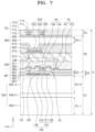
- FIG. 7 is a cross-sectional view of a part of the display device 10 , according to some embodiments.
- the display layer 200 is arranged on the substrate 100 , and a detailed structure of the display layer 200 is the same as that described above with reference to FIG. 5 .
- the display device 10 may include the input detection member TSL arranged on the thin film encapsulation layer 400 .
- the fifth thickness D 5 of the input detection member TSL may be about 0.1 times or less the thickness D from the lower surface of the substrate 100 to the upper surface of the thin film encapsulation layer 400 .
- the neutral plane NP may be located above the second interlayer insulating layer 207 .
- the neutral plane NP may be damaged.
- the input detection member TSL may have a structure in which a first touch conductive layer 711 , a first insulating layer 712 , a second touch conductive layer 713 , and a second insulating layer 714 are sequentially stacked.
- the touch electrode TD may include the first touch conductive layer 711 and the second touch conductive layer 713 . In this state, the first touch conductive layer 711 , the first insulating layer 712 , the second touch conductive layer 713 , and the second insulating layer 714 are the same as those described with reference to FIG. 6 .
- the input detection member TSL may further include a touch buffer layer 716 between the thin film encapsulation layer 400 and the first insulating layer 712 .
- the touch buffer layer 716 may reduce or prevent damage of the thin film encapsulation layer 400 , and may block an interference signal that may be generated during driving of the input detection member TSL.
- the touch buffer layer 716 may include an inorganic material such as silicon oxide, silicon nitride, silicon oxynitride, aluminum oxide, aluminum nitride, titanium oxide, titanium nitride, or the like, or an organic material such as polyimide, polyester, acryl, or the like, and may be formed as a plurality of stacked structures including the above materials.
- the neutral plane NP may be located inside at least one of the first interlayer insulating layer 205 and the second interlayer insulating layer 207 , or below the second interlayer insulating layer 207 .
- the first thickness D 1 may be greater than the second thickness D 2 , the first thickness D 1 may be between about 0.5 times and about 0.76 times the thickness D from the bottom of the substrate 100 to the upper surface of the thin film encapsulation layer 400 .
- the first- 1 thickness D 1 - 1 of the first substrate 100 - 1 and the first- 2 thickness D 1 - 2 of the second substrate 100 - 3 may be the same, or may be different from each other.
- one of the first- 1 thickness D 1 - 1 and the first- 2 thickness D 1 - 2 may be greater than the other of the first- 1 thickness D 1 - 1 and the first- 2 thickness D 1 - 2 .
- the second- 1 thickness D 2 - 1 of the organic encapsulation layer 420 may be between about 0.16 times and about 0.26 times the thickness D from the bottom of the substrate 100 to the upper surface of the thin film encapsulation layer 400 .
- the shock absorbing layer 208 may be arranged on the second interlayer insulating layer 207 . In this state, as the shock absorbing layer 208 is the same as, or similar to, that described with reference to FIG. 4 , a detailed description thereof is omitted.
- the third thickness D 3 of the first interlayer insulating layer 205 may be greater than the fourth thickness D 4 of the second interlayer insulating layer 207 .
- the first interlayer insulating layer 205 may include at least one of silicon oxide and silicon oxynitride, and the second interlayer insulating layer 207 may include silicon nitride.
- the display device 10 may reduce the thickness D 4 of the second interlayer insulating layer 207 where a tensile force is generated, with respect to the neutral plane NP.
- the neutral plane NP is located below the second interlayer insulating layer 207 , and an impact is delivered to the thin film encapsulation layer 400 , as the display device 10 includes the first interlayer insulating layer 205 that endures the tensile force relatively well, the first interlayer insulating layer 205 may not be damaged.
- the force delivered in the thickness direction of the display device 10 may be substantially prevented from being delivered to the first interlayer insulating layer 205 and the second interlayer insulating layer 207 .
- FIG. 8 is a cross-sectional view of a part of the display device 10 , according to some embodiments.
- the display device 10 may include the substrate 100 , the buffer layer 201 , the gate insulating layer 203 , a first transistor 130 a , a second transistor 130 b , the storage capacitor 140 , the first interlayer insulating layer 205 , the second interlayer insulating layer 207 , the shock absorbing layer 208 , the third interlayer insulating layer 209 , the first organic insulating layer 211 , the organic light-emitting diode 220 , the pixel defining layer 215 , and the thin film encapsulation layer 400 .
- the buffer layer 201 , the storage capacitor 140 , the first interlayer insulating layer 205 , the second interlayer insulating layer 207 , the shock absorbing layer 208 , the third interlayer insulating layer 209 , the first organic insulating layer 211 , the organic light-emitting diode 220 , the pixel defining layer 215 , and the thin film encapsulation layer 400 are the same as, or similar to, those described with reference to FIG. 4 , detailed descriptions thereof are omitted.
- the first transistor 130 a may include a first semiconductor layer 134 a and a first gate electrode 136 a .
- the first semiconductor layer 134 a may include a first source region 132 a , a first drain region 133 a , and a first channel region 131 a .
- the first source region 132 a and the first drain region 133 a each may be connected to metals, and the metals may be a first source electrode and a first drain electrode of the first transistor 130 a .
- the first gate electrode 136 a may include a low-resistance metal material.
- the storage capacitor 140 may include the first electrode 144 and the second electrode 146 overlapping each other.
- the first transistor 130 a , the first gate electrode 136 a , and the storage capacitor 140 may be, respectively, the same as, or similar to, the transistor 130 , the gate electrode 136 and the storage capacitor 140 , which are described in FIG. 4 .
- the second transistor 130 b may include a second semiconductor layer 134 b and a second gate electrode 136 b .
- the second semiconductor layer 134 b may include a second source region 132 b , a second drain region 133 b , and a second channel region 131 b .
- the second source region 132 b , the second drain region 133 b , and the second channel region 131 b may respectively correspond to above-described first source region 132 a , first drain region 133 a , and first channel region 131 a.
- a contact metal layer CM may connect the pixel electrode 221 to the second drain region 133 b .
- separate metals may be connected to the second source region 132 b and the second drain region 133 b , and the metals may be a second source electrode SR 2 and a second drain electrode DR 2 .
- one of the second source electrode SR 2 and the second drain electrode DR 2 may be connected to the contact metal layer CM.
- the contact metal layer CM is connected to the second drain region 133 b through the second drain electrode DR 2 is mainly described.
- the second gate electrode 136 b may be arranged on the second semiconductor layer 134 b .
- the gate insulating layer 203 may be arranged between the second gate electrode 136 b and the second semiconductor layer 134 b .
- the second gate electrode 136 b may be the same as, or similar to, the first gate electrode 136 a.
- the relationship between the first thickness D 1 , the second thickness D 2 , the third thickness D 3 , the fourth thickness D 4 , and the thickness D may be adopted in the same or similar manner. Furthermore, the above-described relationship may be identically applied to the relationship between the first- 1 thickness D 1 - 1 and the first- 2 thickness D 1 - 2 and the relationship between the second- 1 thickness D 2 - 1 and the thickness D.
- the location of the neutral plane NP may be located between the first interlayer insulating layer 205 and the second interlayer insulating layer 207 or below the first interlayer insulating layer 205 .
- the display device 10 effectively absorbs the impact during falling of an object, even when an object falls onto the display device 10 , the display device 10 may not be broken or damaged. Furthermore, as the display device 10 has no area where a tensile force is generated when colliding with an object, and/or as the first interlayer insulating layer 205 and the second interlayer insulating layer 207 are less present in the area where a tensile force is generated, damage of at least one of the first interlayer insulating layer 205 and the second interlayer insulating layer 207 may be reduced or prevented.
- FIG. 9 is a cross-sectional view of a part of the display device 10 , according to some embodiments.
- the display device 10 may include the substrate 100 , the buffer layer 201 , the gate insulating layer 203 , the first transistor 130 a , the second transistor 130 b , the storage capacitor 140 , the first interlayer insulating layer 205 , the second interlayer insulating layer 207 , the shock absorbing layer 208 , the third interlayer insulating layer 209 , the first organic insulating layer 211 , the organic light-emitting diode 220 , the pixel defining layer 215 , the thin film encapsulation layer 400 , and the input detection member TSL.
- the substrate 100 , the buffer layer 201 , the first transistor 130 a , the second transistor 130 b , the storage capacitor 140 , the first interlayer insulating layer 205 , the second interlayer insulating layer 207 , the shock absorbing layer 208 , the third interlayer insulating layer 209 , the first organic insulating layer 211 , the organic light-emitting diode 220 , the pixel defining layer 215 , and the thin film encapsulation layer 400 may be the same as, or similar to, those described with reference to FIG. 8 .
- the input detection member TSL may be arranged on the upper surface of the thin film encapsulation layer 400 .
- the input detection member TSL may have a structure in which the first touch conductive layer 711 , the first insulating layer 712 , the second touch conductive layer 713 , and the second insulating layer 714 are sequentially stacked.
- the input detection member TSL is the same as, or similar to, that described with reference to FIG. 6 , a detailed description thereof is omitted.
- the relationship between the first thickness D 1 , the second thickness D 2 , the third thickness D 3 , the fourth thickness D 4 , and the thickness D may be adopted in the same or similar manner. Furthermore, the relationships described with reference to FIGS. 4 and 6 may be identically applied as the relationship between the first- 1 thickness D 1 - 1 and the first- 2 thickness D 1 - 2 , the relationship between the second- 1 thickness D 2 - 1 and the thickness D, and the relationship between the fifth thickness D 5 and the thickness D.
- the display device 10 may reduce the thickness D 4 of the second interlayer insulating layer 207 where a tensile force is generated, with respect to the neutral plane NP.
- the neutral plane NP is located below the second interlayer insulating layer 207 , and an impact is delivered to the thin film encapsulation layer 400 , as the display device 10 includes the first interlayer insulating layer 205 that endures the tensile force well, the first interlayer insulating layer 205 may not be damaged.
- the force delivered in the thickness direction of the display device 10 may be prevented from being delivered to the first interlayer insulating layer 205 and the second interlayer insulating layer 207 .
- FIG. 10 is a cross-sectional view of a part of the display device 10 , according to some embodiments.
- the display device 10 may include the substrate 100 , the buffer layer 201 , the gate insulating layer 203 , the first transistor 130 a , the second transistor 130 b , the storage capacitor 140 , the first interlayer insulating layer 205 , the second interlayer insulating layer 207 , the shock absorbing layer 208 , the third interlayer insulating layer 209 , the first organic insulating layer 211 , the organic light-emitting diode 220 , the pixel defining layer 215 , the thin film encapsulation layer 400 , and the input detection member TSL.
- the substrate 100 , the buffer layer 201 , the first transistor 130 a , the second transistor 130 b , the storage capacitor 140 , the first interlayer insulating layer 205 , the second interlayer insulating layer 207 , the shock absorbing layer 208 , the third interlayer insulating layer 209 , the first organic insulating layer 211 , the organic light-emitting diode 220 , the pixel defining layer 215 , and the thin film encapsulation layer 400 may be the same as, or similar to, those described with reference to FIG. 8 .
- the input detection member TSL may be arranged on the upper surface of the thin film encapsulation layer 400 .
- the input detection member TSL may have a structure in which the first touch conductive layer 711 , the first insulating layer 712 , the second touch conductive layer 713 , and the second insulating layer 714 , and a touch buffer layer 716 are sequentially stacked.
- the input detection member TSL is the same as, or similar to, that described with reference to FIG. 7 , a detailed description thereof is omitted.
- the relationship between the first thickness D 1 , the second thickness D 2 , the third thickness D 3 , the fourth thickness D 4 , and the thickness D may be adopted in the same or similar manner. Furthermore, the relationships described with reference to FIGS. 4 and 7 may be identically applied as the relationship between the first- 1 thickness D 1 - 1 and the first- 2 thickness D 1 - 2 , the relationship between the second- 1 thickness D 2 - 1 and the thickness D, and the relationship between the fifth thickness D 5 and the thickness D.
- the display device 10 may reduce the thickness D 4 of the second interlayer insulating layer 207 where a tensile force is generated with respect to the neutral plane NP.
- the neutral plane NP is located below the second interlayer insulating layer 207 , and an impact is delivered to the thin film encapsulation layer 400 , as the display device 10 includes the first interlayer insulating layer 205 that endures the tensile force relatively well, the first interlayer insulating layer 205 may not be damaged.
- the display device 10 includes the shock absorbing layer 208 , delivery of the force, which is delivered in the thickness direction of the display device 10 , to the first interlayer insulating layer 205 and the second interlayer insulating layer 207 may be reduced or prevented.
- FIG. 11 is a cross-sectional view of a part of the display device 10 , according to some embodiments.
- the display device 10 may include the substrate 100 , the buffer layer 201 , a first gate insulating layer 203 - 1 , the first transistor 130 a , the second transistor 130 b , the storage capacitor 140 , the first interlayer insulating layer 205 , a shielding layer 150 , the second interlayer insulating layer 207 , a second gate insulating layer 203 - 2 , the shock absorbing layer 208 , the third interlayer insulating layer 209 , the first organic insulating layer 211 , the organic light-emitting diode 220 , the pixel defining layer 215 , the thin film encapsulation layer 400 , and the input detection member TSL.
- the substrate 100 and the buffer layer 201 may be the same as, or similar to, those described with reference to FIG. 8 .
- the first transistor 130 a may include the first semiconductor layer 134 a and the first gate electrode 136 a .
- the first semiconductor layer 134 a may be arranged on the buffer layer 201 , and covered by the first gate insulating layer 203 - 1 .
- the first semiconductor layer 134 a may include the first source region 132 a , the first channel region 131 a , and the first drain region 133 a .
- one of the first source region 132 a and the first drain region 133 a may be connected to the pixel electrode 221 through the contact metal layer CM.
- the first source region 132 a when the first source region 132 a is connected to the pixel electrode 221 , the first source region 132 a may be connected to the contact metal layer CM through a first source electrode SR 1 connected to the first source region 132 a , and the contact metal layer CM may be connected to the pixel electrode 221 .
- the first drain region 133 a may be connected to the pixel electrode 221 through a first drain electrode DR 1 and the contact metal layer CM.
- a case in which the first source region 132 a is connected to the pixel electrode 221 is mainly described.
- the first gate insulating layer 203 - 1 may include an inorganic material including oxide or nitride.
- the first gate insulating layer 203 - 1 may include silicon oxide (SiO 2 ), silicon nitride (SiN x ), silicon oxynitride (SiON), aluminum oxide (Al 2 O 3 ), titanium oxide (TiO 2 ), tantalum oxide (Ta 2 O 5 ), hafnium oxide (HfO 2 ), zinc oxide (ZnO 2 ), and the like.
- the first gate electrode 136 a may be arranged on the first gate insulating layer 203 - 1 . In this state, the first gate electrode 136 a may function as the first electrode 144 of the storage capacitor 140 .
- the first interlayer insulating layer 205 may be arranged on the first gate electrode 136 a . In this state, the first interlayer insulating layer 205 may be the same as, or similar to, that described with reference to FIG. 8 .
- the shielding layer 150 as above may be arranged on the first interlayer insulating layer 205 . In this state, the shielding layer 150 is arranged below the second transistor 130 b to apply an appropriate voltage, and thus the second transistor 130 b may not be affected by external light and the electric potential of the substrate 100 . In some embodiments, the shielding layer 150 may be arranged below the first transistor 130 a .
- the shielding layer 150 may include metal, and may include a single layer or a multilayer.
- the shielding layer 150 may have a single layer structure including Mo.
- the shielding layer 150 may have, above the buffer layer 201 , a three-layer structure sequentially including a first layer having Ti, a second layer having Al, and a third layer having Ti.
- the second electrode 146 of the storage capacitor 140 may be arranged on the first interlayer insulating layer 205 as above.
- the second interlayer insulating layer 207 may be arranged on the shielding layer 150 and the second electrode 146 . In this state, the second interlayer insulating layer 207 may be the same as, or similar to, that described with reference to FIG. 8 .
- the second semiconductor layer 134 b of the second transistor 130 b may be arranged on the second interlayer insulating layer 207 .
- the second semiconductor layer 134 b may include the second source region 132 b , the second channel region 131 b , and the second drain region 133 b .
- the second source region 132 b and the second drain region 133 b may be connected to a metal layer, and the metal layer may function as the second source electrode SR 2 and the second drain electrode DR 2 .
- the second gate insulating layer 203 - 2 may be arranged on the second semiconductor layer 134 b as above. In this state, the second gate insulating layer 203 - 2 may be the same as, or similar to, the first gate insulating layer 203 - 1 .
- the second gate electrode 136 b may be arranged on the second gate insulating layer 203 - 2 . In this state, as the second gate electrode 136 b is the same as, or similar to, that described with reference to FIG. 8 , a detailed description thereof is omitted.
- the second gate electrode 136 b may be covered by the third interlayer insulating layer 209 .
- the third interlayer insulating layer 209 may be the same as, or similar to, at least one of the first interlayer insulating layer 205 and the second interlayer insulating layer 207 that are described above.
- the shock absorbing layer 208 may be arranged on the third interlayer insulating layer 209 .
- the shock absorbing layer 208 may include an organic material, and may be the same as, or similar to, that described with reference to FIG. 8 .
- the contact metal layer CM may be arranged on the shock absorbing layer 208 as above. Furthermore, the first organic insulating layer 211 and the second organic insulating layer 213 may be sequentially arranged on the contact metal layer CM. In this state, as the first organic insulating layer 211 and the second organic insulating layer 213 are the same as, or similar to, those described with reference to FIG. 4 , detailed descriptions thereof are omitted.
- the organic light-emitting diode 220 may include the pixel electrode 221 , the intermediate layer 222 , and the counter electrode 223 .
- the pixel electrode 221 may be connected to the first source region 132 a or the first drain region 133 a of the first transistor 130 a , or to the second source region 132 b or the second drain region 133 b of the second transistor 130 b , through the contact metal layer CM.
- a detailed description thereof is omitted.
- a case in which the first source region 132 a is connected to the pixel electrode 221 is mainly described.
- the thin film encapsulation layer 400 may be arranged on the organic light-emitting diode 220 .
- the thin film encapsulation layer 400 may include the first inorganic encapsulation layer 410 , the organic encapsulation layer 420 , and the second inorganic encapsulation layer 430 , which are sequentially stacked. In this state, as the thin film encapsulation layer 400 is the same as, or similar to, that described with reference to FIG. 4 , a detailed description thereof is omitted.
- the relationship between the first thickness D 1 , the second thickness D 2 , the third thickness D 3 , the fourth thickness D 4 , and the thickness D may be adopted in the same or similar manner. Furthermore, the relationships described with reference to FIGS. 4 and 7 may be identically applied as the relationship between the first- 1 thickness D 1 - 1 and the first- 2 thickness D 1 - 2 and the relationship between the second- 1 thickness D 2 - 1 and the thickness D.
- the display device 10 may further include an input detection member.
- the input detection member may be arranged on the thin film encapsulation layer 400 , as illustrated in FIGS. 9 and 10 .
- the relationship between the fifth thickness D 5 and the thickness D may have the same as that described with reference to FIGS. 9 and 10 .
- the display device 10 may reduce the thickness D 4 of the second interlayer insulating layer 207 where a tensile force is generated, with respect to the neutral plane NP.
- the neutral plane NP is located below the second interlayer insulating layer 207 , and an impact is delivered to the thin film encapsulation layer 400 , as the display device 10 includes the first interlayer insulating layer 205 that endures the tensile force well, the first interlayer insulating layer 205 may not be damaged.
- the force delivered in the thickness direction of the display device 10 may be prevented from being delivered to the first interlayer insulating layer 205 and the second interlayer insulating layer 207 .
- dark spots may prevented despite an impact that is externally applied.
- a display device may be freely modified, and some layers in the display device may be prevented from being broken or damaged during modification.
- an external impact may be effectively processed.
Landscapes
- Engineering & Computer Science (AREA)
- Microelectronics & Electronic Packaging (AREA)
- Physics & Mathematics (AREA)
- Optics & Photonics (AREA)
- Electroluminescent Light Sources (AREA)
- Devices For Indicating Variable Information By Combining Individual Elements (AREA)
Abstract
Description
Claims (20)
Priority Applications (1)
| Application Number | Priority Date | Filing Date | Title |
|---|---|---|---|
| US19/030,929 US20250176409A1 (en) | 2021-04-12 | 2025-01-17 | Electronic device |
Applications Claiming Priority (2)
| Application Number | Priority Date | Filing Date | Title |
|---|---|---|---|
| KR10-2021-0047338 | 2021-04-12 | ||
| KR1020210047338A KR20220141386A (en) | 2021-04-12 | 2021-04-12 | Display device |
Related Child Applications (1)
| Application Number | Title | Priority Date | Filing Date |
|---|---|---|---|
| US19/030,929 Continuation-In-Part US20250176409A1 (en) | 2021-04-12 | 2025-01-17 | Electronic device |
Publications (2)
| Publication Number | Publication Date |
|---|---|
| US20220328586A1 US20220328586A1 (en) | 2022-10-13 |
| US12238978B2 true US12238978B2 (en) | 2025-02-25 |
Family
ID=83509553
Family Applications (1)
| Application Number | Title | Priority Date | Filing Date |
|---|---|---|---|
| US17/521,476 Active 2042-10-04 US12238978B2 (en) | 2021-04-12 | 2021-11-08 | Display device including shock absorbing layer |
Country Status (3)
| Country | Link |
|---|---|
| US (1) | US12238978B2 (en) |
| KR (1) | KR20220141386A (en) |
| CN (2) | CN217822811U (en) |
Citations (20)
| Publication number | Priority date | Publication date | Assignee | Title |
|---|---|---|---|---|
| US20150195915A1 (en) | 2014-01-06 | 2015-07-09 | Samsung Display Co., Ltd. | Display device and method for manufacturing the same |
| US20160204347A1 (en) * | 2014-08-14 | 2016-07-14 | Samsung Display Co., Ltd. | Display device and method for manufacturing the same |
| US20170047545A1 (en) * | 2015-08-12 | 2017-02-16 | Samsung Display Co., Ltd. | Display device |
| US20170117487A1 (en) * | 2015-10-23 | 2017-04-27 | Semiconductor Energy Laboratory Co., Ltd. | Heterocyclic Compound, Light-Emitting Element, Light-Emitting Device, Electronic Device, and Lighting Device |
| US20170186971A1 (en) * | 2015-12-25 | 2017-06-29 | Semiconductor Energy Laboratory Co., Ltd. | Compound, Light-Emitting Element, Display Device, Electronic Device, and Lighting Device |
| US9865665B2 (en) | 2014-05-02 | 2018-01-09 | Semiconductor Energy Laboratory Co., Ltd. | Semiconductor device, input/output device, and electronic appliance |
| KR20180045888A (en) | 2012-05-09 | 2018-05-04 | 가부시키가이샤 한도오따이 에네루기 켄큐쇼 | Light-emitting device and electronic device |
| US20180175310A1 (en) * | 2016-10-17 | 2018-06-21 | Samsung Display Co., Ltd. | Display device and method of manufacturing the same |
| US20180350893A1 (en) * | 2017-06-02 | 2018-12-06 | Japan Display Inc. | Display device and method of manufacturing a display device |
| US20190165060A1 (en) * | 2017-11-28 | 2019-05-30 | Lg Display Co., Ltd. | Foldable Display Device |
| US10312461B2 (en) | 2017-10-30 | 2019-06-04 | Wuhan China Star Optoelectronics Semiconductor Display Technology Co., Ltd. | Flexible OLED display panel having a substrate with a titanium layer and method for manufacturing same |
| US20190207133A1 (en) * | 2017-12-28 | 2019-07-04 | Samsung Display Co., Ltd. | Display apparatus |
| US20190361550A1 (en) * | 2017-01-25 | 2019-11-28 | Sharp Kabushiki Kaisha | Oled panel |
| US20200075895A1 (en) * | 2018-08-28 | 2020-03-05 | Samsung Display Co., Ltd. | Foldable display device |
| US20200110495A1 (en) * | 2018-10-05 | 2020-04-09 | Samsung Display Co., Ltd. | Display device |
| US20200252707A1 (en) * | 2019-02-01 | 2020-08-06 | Samsung Display Co., Ltd. | Display device |
| KR20200115807A (en) | 2019-03-26 | 2020-10-08 | 삼성디스플레이 주식회사 | Display device |
| KR20200144626A (en) | 2019-06-18 | 2020-12-30 | 삼성디스플레이 주식회사 | Display apparatus |
| US20200411598A1 (en) * | 2019-06-28 | 2020-12-31 | Lg Display Co., Ltd. | Display Device |
| US20210202868A1 (en) * | 2019-12-31 | 2021-07-01 | Lg Display Co., Ltd. | Display apparatus |
-
2021
- 2021-04-12 KR KR1020210047338A patent/KR20220141386A/en not_active Ceased
- 2021-11-08 US US17/521,476 patent/US12238978B2/en active Active
-
2022
- 2022-04-12 CN CN202220833497.5U patent/CN217822811U/en active Active
- 2022-04-12 CN CN202210379108.0A patent/CN115207047A/en active Pending
Patent Citations (25)
| Publication number | Priority date | Publication date | Assignee | Title |
|---|---|---|---|---|
| KR20180045888A (en) | 2012-05-09 | 2018-05-04 | 가부시키가이샤 한도오따이 에네루기 켄큐쇼 | Light-emitting device and electronic device |
| KR20200115446A (en) | 2012-05-09 | 2020-10-07 | 가부시키가이샤 한도오따이 에네루기 켄큐쇼 | Light-emitting device and electronic device |
| US10003047B2 (en) | 2012-05-09 | 2018-06-19 | Semiconductor Energy Laboratory Co., Ltd. | Light-emitting device and electronic device |
| KR20150081563A (en) | 2014-01-06 | 2015-07-15 | 삼성디스플레이 주식회사 | Display device and method for manufacturing the same |
| US20150195915A1 (en) | 2014-01-06 | 2015-07-09 | Samsung Display Co., Ltd. | Display device and method for manufacturing the same |
| JP2020160452A (en) | 2014-05-02 | 2020-10-01 | 株式会社半導体エネルギー研究所 | Input-output device |
| US9865665B2 (en) | 2014-05-02 | 2018-01-09 | Semiconductor Energy Laboratory Co., Ltd. | Semiconductor device, input/output device, and electronic appliance |
| US20160204347A1 (en) * | 2014-08-14 | 2016-07-14 | Samsung Display Co., Ltd. | Display device and method for manufacturing the same |
| US20170047545A1 (en) * | 2015-08-12 | 2017-02-16 | Samsung Display Co., Ltd. | Display device |
| US20170117487A1 (en) * | 2015-10-23 | 2017-04-27 | Semiconductor Energy Laboratory Co., Ltd. | Heterocyclic Compound, Light-Emitting Element, Light-Emitting Device, Electronic Device, and Lighting Device |
| US20170186971A1 (en) * | 2015-12-25 | 2017-06-29 | Semiconductor Energy Laboratory Co., Ltd. | Compound, Light-Emitting Element, Display Device, Electronic Device, and Lighting Device |
| US20180175310A1 (en) * | 2016-10-17 | 2018-06-21 | Samsung Display Co., Ltd. | Display device and method of manufacturing the same |
| US20190361550A1 (en) * | 2017-01-25 | 2019-11-28 | Sharp Kabushiki Kaisha | Oled panel |
| US20180350893A1 (en) * | 2017-06-02 | 2018-12-06 | Japan Display Inc. | Display device and method of manufacturing a display device |
| US10312461B2 (en) | 2017-10-30 | 2019-06-04 | Wuhan China Star Optoelectronics Semiconductor Display Technology Co., Ltd. | Flexible OLED display panel having a substrate with a titanium layer and method for manufacturing same |
| US20190165060A1 (en) * | 2017-11-28 | 2019-05-30 | Lg Display Co., Ltd. | Foldable Display Device |
| US20190207133A1 (en) * | 2017-12-28 | 2019-07-04 | Samsung Display Co., Ltd. | Display apparatus |
| US20200075895A1 (en) * | 2018-08-28 | 2020-03-05 | Samsung Display Co., Ltd. | Foldable display device |
| US20200110495A1 (en) * | 2018-10-05 | 2020-04-09 | Samsung Display Co., Ltd. | Display device |
| US20200252707A1 (en) * | 2019-02-01 | 2020-08-06 | Samsung Display Co., Ltd. | Display device |
| KR20200115807A (en) | 2019-03-26 | 2020-10-08 | 삼성디스플레이 주식회사 | Display device |
| US11016622B2 (en) | 2019-03-26 | 2021-05-25 | Samsung Display Co., Ltd. | Display device |
| KR20200144626A (en) | 2019-06-18 | 2020-12-30 | 삼성디스플레이 주식회사 | Display apparatus |
| US20200411598A1 (en) * | 2019-06-28 | 2020-12-31 | Lg Display Co., Ltd. | Display Device |
| US20210202868A1 (en) * | 2019-12-31 | 2021-07-01 | Lg Display Co., Ltd. | Display apparatus |
Also Published As
| Publication number | Publication date |
|---|---|
| CN115207047A (en) | 2022-10-18 |
| CN217822811U (en) | 2022-11-15 |
| US20220328586A1 (en) | 2022-10-13 |
| KR20220141386A (en) | 2022-10-20 |
Similar Documents
| Publication | Publication Date | Title |
|---|---|---|
| US10804340B2 (en) | Display device with light transmission control layer | |
| US11683951B2 (en) | Display panel and display device | |
| US12052886B2 (en) | Display apparatus having a refractive layer | |
| EP3800667B1 (en) | Display device | |
| US11678537B2 (en) | Display apparatus | |
| US20250048876A1 (en) | Display panel and display apparatus | |
| US12386104B2 (en) | Cover window and display apparatus including the same | |
| US12446443B2 (en) | Display panel and display device | |
| US20250324864A1 (en) | Display apparatus and method of manufacturing the same | |
| US11985868B2 (en) | Display apparatus | |
| US12289963B2 (en) | Display device and method of manufacturing the same | |
| US20230371345A1 (en) | Display panel and method of manufacturing display panel | |
| US12238978B2 (en) | Display device including shock absorbing layer | |
| US20250176409A1 (en) | Electronic device | |
| US12342700B2 (en) | Display apparatus | |
| US20250294975A1 (en) | Light-emitting diode, display device including the same, and electronic device including the same | |
| US20250271598A1 (en) | Anti-reflection layer and display apparatus having the same | |
| US20250120274A1 (en) | Display device | |
| US20230200118A1 (en) | Display apparatus and method of manufacturing the display apparatus | |
| CN115720465A (en) | Display device |
Legal Events
| Date | Code | Title | Description |
|---|---|---|---|
| FEPP | Fee payment procedure |
Free format text: ENTITY STATUS SET TO UNDISCOUNTED (ORIGINAL EVENT CODE: BIG.); ENTITY STATUS OF PATENT OWNER: LARGE ENTITY |
|
| AS | Assignment |
Owner name: SAMSUNG DISPLAY CO., LTD., KOREA, REPUBLIC OF Free format text: ASSIGNMENT OF ASSIGNORS INTEREST;ASSIGNORS:CHOI, WONWOO;KIM, INBAE;NAM, DONGHUN;AND OTHERS;REEL/FRAME:058086/0328 Effective date: 20210924 |
|
| STPP | Information on status: patent application and granting procedure in general |
Free format text: DOCKETED NEW CASE - READY FOR EXAMINATION |
|
| STPP | Information on status: patent application and granting procedure in general |
Free format text: NON FINAL ACTION MAILED |
|
| STPP | Information on status: patent application and granting procedure in general |
Free format text: RESPONSE TO NON-FINAL OFFICE ACTION ENTERED AND FORWARDED TO EXAMINER |
|
| STPP | Information on status: patent application and granting procedure in general |
Free format text: NOTICE OF ALLOWANCE MAILED -- APPLICATION RECEIVED IN OFFICE OF PUBLICATIONS |
|
| ZAAB | Notice of allowance mailed |
Free format text: ORIGINAL CODE: MN/=. |
|
| STPP | Information on status: patent application and granting procedure in general |
Free format text: PUBLICATIONS -- ISSUE FEE PAYMENT VERIFIED |
|
| STCF | Information on status: patent grant |
Free format text: PATENTED CASE |