US12236998B2 - Semiconductor device - Google Patents
Semiconductor device Download PDFInfo
- Publication number
- US12236998B2 US12236998B2 US18/143,127 US202318143127A US12236998B2 US 12236998 B2 US12236998 B2 US 12236998B2 US 202318143127 A US202318143127 A US 202318143127A US 12236998 B2 US12236998 B2 US 12236998B2
- Authority
- US
- United States
- Prior art keywords
- word line
- voltage
- level
- semiconductor device
- initial level
- Prior art date
- Legal status (The legal status is an assumption and is not a legal conclusion. Google has not performed a legal analysis and makes no representation as to the accuracy of the status listed.)
- Active, expires
Links
Images


Classifications
-
- G—PHYSICS
- G11—INFORMATION STORAGE
- G11C—STATIC STORES
- G11C11/00—Digital stores characterised by the use of particular electric or magnetic storage elements; Storage elements therefor
- G11C11/21—Digital stores characterised by the use of particular electric or magnetic storage elements; Storage elements therefor using electric elements
- G11C11/34—Digital stores characterised by the use of particular electric or magnetic storage elements; Storage elements therefor using electric elements using semiconductor devices
- G11C11/40—Digital stores characterised by the use of particular electric or magnetic storage elements; Storage elements therefor using electric elements using semiconductor devices using transistors
- G11C11/401—Digital stores characterised by the use of particular electric or magnetic storage elements; Storage elements therefor using electric elements using semiconductor devices using transistors forming cells needing refreshing or charge regeneration, i.e. dynamic cells
- G11C11/4063—Auxiliary circuits, e.g. for addressing, decoding, driving, writing, sensing or timing
- G11C11/407—Auxiliary circuits, e.g. for addressing, decoding, driving, writing, sensing or timing for memory cells of the field-effect type
- G11C11/408—Address circuits
- G11C11/4085—Word line control circuits, e.g. word line drivers, - boosters, - pull-up, - pull-down, - precharge
-
- G—PHYSICS
- G11—INFORMATION STORAGE
- G11C—STATIC STORES
- G11C11/00—Digital stores characterised by the use of particular electric or magnetic storage elements; Storage elements therefor
- G11C11/21—Digital stores characterised by the use of particular electric or magnetic storage elements; Storage elements therefor using electric elements
- G11C11/34—Digital stores characterised by the use of particular electric or magnetic storage elements; Storage elements therefor using electric elements using semiconductor devices
- G11C11/40—Digital stores characterised by the use of particular electric or magnetic storage elements; Storage elements therefor using electric elements using semiconductor devices using transistors
- G11C11/401—Digital stores characterised by the use of particular electric or magnetic storage elements; Storage elements therefor using electric elements using semiconductor devices using transistors forming cells needing refreshing or charge regeneration, i.e. dynamic cells
- G11C11/4063—Auxiliary circuits, e.g. for addressing, decoding, driving, writing, sensing or timing
- G11C11/407—Auxiliary circuits, e.g. for addressing, decoding, driving, writing, sensing or timing for memory cells of the field-effect type
- G11C11/408—Address circuits
- G11C11/4087—Address decoders, e.g. bit - or word line decoders; Multiple line decoders
-
- G—PHYSICS
- G11—INFORMATION STORAGE
- G11C—STATIC STORES
- G11C11/00—Digital stores characterised by the use of particular electric or magnetic storage elements; Storage elements therefor
- G11C11/21—Digital stores characterised by the use of particular electric or magnetic storage elements; Storage elements therefor using electric elements
- G11C11/34—Digital stores characterised by the use of particular electric or magnetic storage elements; Storage elements therefor using electric elements using semiconductor devices
- G11C11/40—Digital stores characterised by the use of particular electric or magnetic storage elements; Storage elements therefor using electric elements using semiconductor devices using transistors
- G11C11/401—Digital stores characterised by the use of particular electric or magnetic storage elements; Storage elements therefor using electric elements using semiconductor devices using transistors forming cells needing refreshing or charge regeneration, i.e. dynamic cells
- G11C11/4063—Auxiliary circuits, e.g. for addressing, decoding, driving, writing, sensing or timing
- G11C11/407—Auxiliary circuits, e.g. for addressing, decoding, driving, writing, sensing or timing for memory cells of the field-effect type
- G11C11/409—Read-write [R-W] circuits
- G11C11/4091—Sense or sense/refresh amplifiers, or associated sense circuitry, e.g. for coupled bit-line precharging, equalising or isolating
-
- G—PHYSICS
- G11—INFORMATION STORAGE
- G11C—STATIC STORES
- G11C11/00—Digital stores characterised by the use of particular electric or magnetic storage elements; Storage elements therefor
- G11C11/21—Digital stores characterised by the use of particular electric or magnetic storage elements; Storage elements therefor using electric elements
- G11C11/34—Digital stores characterised by the use of particular electric or magnetic storage elements; Storage elements therefor using electric elements using semiconductor devices
- G11C11/40—Digital stores characterised by the use of particular electric or magnetic storage elements; Storage elements therefor using electric elements using semiconductor devices using transistors
- G11C11/41—Digital stores characterised by the use of particular electric or magnetic storage elements; Storage elements therefor using electric elements using semiconductor devices using transistors forming static cells with positive feedback, i.e. cells not needing refreshing or charge regeneration, e.g. bistable multivibrator or Schmitt trigger
- G11C11/413—Auxiliary circuits, e.g. for addressing, decoding, driving, writing, sensing, timing or power reduction
- G11C11/417—Auxiliary circuits, e.g. for addressing, decoding, driving, writing, sensing, timing or power reduction for memory cells of the field-effect type
- G11C11/418—Address circuits
-
- G—PHYSICS
- G11—INFORMATION STORAGE
- G11C—STATIC STORES
- G11C8/00—Arrangements for selecting an address in a digital store
- G11C8/08—Word line control circuits, e.g. drivers, boosters, pull-up circuits, pull-down circuits, precharging circuits, for word lines
-
- H—ELECTRICITY
- H01—ELECTRIC ELEMENTS
- H01L—SEMICONDUCTOR DEVICES NOT COVERED BY CLASS H10
- H01L25/00—Assemblies consisting of a plurality of semiconductor or other solid state devices
- H01L25/03—Assemblies consisting of a plurality of semiconductor or other solid state devices all the devices being of a type provided for in a single subclass of subclasses H10B, H10D, H10F, H10H, H10K or H10N, e.g. assemblies of rectifier diodes
- H01L25/04—Assemblies consisting of a plurality of semiconductor or other solid state devices all the devices being of a type provided for in a single subclass of subclasses H10B, H10D, H10F, H10H, H10K or H10N, e.g. assemblies of rectifier diodes the devices not having separate containers
- H01L25/065—Assemblies consisting of a plurality of semiconductor or other solid state devices all the devices being of a type provided for in a single subclass of subclasses H10B, H10D, H10F, H10H, H10K or H10N, e.g. assemblies of rectifier diodes the devices not having separate containers the devices being of a type provided for in group H10D89/00
- H01L25/0655—Assemblies consisting of a plurality of semiconductor or other solid state devices all the devices being of a type provided for in a single subclass of subclasses H10B, H10D, H10F, H10H, H10K or H10N, e.g. assemblies of rectifier diodes the devices not having separate containers the devices being of a type provided for in group H10D89/00 the devices being arranged next to each other
-
- H—ELECTRICITY
- H10—SEMICONDUCTOR DEVICES; ELECTRIC SOLID-STATE DEVICES NOT OTHERWISE PROVIDED FOR
- H10B—ELECTRONIC MEMORY DEVICES
- H10B12/00—Dynamic random access memory [DRAM] devices
- H10B12/30—DRAM devices comprising one-transistor - one-capacitor [1T-1C] memory cells
- H10B12/48—Data lines or contacts therefor
- H10B12/482—Bit lines
-
- H—ELECTRICITY
- H10—SEMICONDUCTOR DEVICES; ELECTRIC SOLID-STATE DEVICES NOT OTHERWISE PROVIDED FOR
- H10B—ELECTRONIC MEMORY DEVICES
- H10B12/00—Dynamic random access memory [DRAM] devices
- H10B12/30—DRAM devices comprising one-transistor - one-capacitor [1T-1C] memory cells
- H10B12/48—Data lines or contacts therefor
- H10B12/488—Word lines
-
- H—ELECTRICITY
- H10—SEMICONDUCTOR DEVICES; ELECTRIC SOLID-STATE DEVICES NOT OTHERWISE PROVIDED FOR
- H10B—ELECTRONIC MEMORY DEVICES
- H10B12/00—Dynamic random access memory [DRAM] devices
- H10B12/50—Peripheral circuit region structures
-
- H—ELECTRICITY
- H10—SEMICONDUCTOR DEVICES; ELECTRIC SOLID-STATE DEVICES NOT OTHERWISE PROVIDED FOR
- H10B—ELECTRONIC MEMORY DEVICES
- H10B80/00—Assemblies of multiple devices comprising at least one memory device covered by this subclass
-
- H10W90/00—
-
- G—PHYSICS
- G11—INFORMATION STORAGE
- G11C—STATIC STORES
- G11C8/00—Arrangements for selecting an address in a digital store
- G11C8/10—Decoders
Definitions
- a semiconductor device including a memory cell array that includes a plurality of memory cells electrically connected to a plurality of word lines and a plurality of bit lines, a word line driving circuit that includes a plurality of sub-word line decoders electrically connected to the plurality of word lines, and a control logic configured to determine a selected word line and unselected word lines among the plurality of word lines, and configured to control the word line driving circuit such that at least one of the unselected word lines that is adjacent to the selected word line is floated during at least a portion of a period in which a voltage of the selected word line returns to an initial level.
- a semiconductor device including a memory cell array that includes a plurality of memory cells electrically connected to a plurality of word lines and a plurality of bit lines, and a peripheral circuit configured to control the memory cell array.
- the peripheral circuit may be configured to perform a control operation for a selected memory cell among the plurality of memory cells through a selected bit line among the plurality of bit lines while a voltage of a selected word line among the plurality of word lines is maintained at an active level, and set a voltage of at least one unselected word line, adjacent to the selected word line, among the plurality of word lines to a level lower than an initial level during at least a portion of a period in which the voltage of the selected word line decreases from the active level to the initial level.
- a control operation may be performed on a selected memory cell by activating a selected word line, and at least one unselected word line, adjacent to the selected word line, may be caused to float while a voltage of the selected word line is reduced from an active level to an initial level. Accordingly, a voltage of the unselected word line may decrease to a level lower than the initial level, and then may return to the initial level, and data loss of unselected memory cells connected to the unselected word line may be minimized, thereby improving reliability of a semiconductor device.
- FIG. 1 is a schematic block diagram illustrating a semiconductor device according to example embodiments of the present disclosure
- FIG. 2 is a schematic diagram illustrating a structure of a semiconductor device according to example embodiments of the present disclosure
- FIGS. 3 and 4 are schematic diagrams illustrating a structure of a portion of a memory cell array included in a semiconductor device according to example embodiments of the present disclosure
- FIG. 5 is a diagram illustrating an operation of a semiconductor device according to example embodiments of the present disclosure.
- FIGS. 6 and 7 are schematic diagrams illustrating a sub-word line decoder included in a semiconductor device according to example embodiments of the present disclosure
- FIG. 9 is a diagram illustrating an operation of a semiconductor device according to example embodiments of the present disclosure.
- FIG. 10 is a schematic diagram illustrating a semiconductor device according to example embodiments of the present disclosure.
- FIGS. 11 to 13 are diagrams illustrating an operation of a semiconductor device according to example embodiments of the present disclosure.
- FIGS. 14 to 16 are diagrams illustrating an operation of a semiconductor device according to example embodiments of the present disclosure.
- FIGS. 17 and 18 are diagrams illustrating an operation of a semiconductor device according to example embodiments of the present disclosure.
- FIG. 1 is a schematic block diagram illustrating a semiconductor device according to example embodiments of the present disclosure.
- a semiconductor device 10 may be a storage device based on a semiconductor element.
- the semiconductor device 10 may be a random access memory (RAM) device such as dynamic random access memory (DRAM), synchronous DRAM (SDRAM), static RAM (SRAM), double date rate SDRAM (DDR SDRAM), DDR2 SDRAM, DDR3 SDRAM, phase-change RAM (PRAM), magnetic RAM (MRAM), resistive RAM (RRAM), or the like.
- DRAM dynamic random access memory
- SDRAM synchronous DRAM
- SRAM static RAM
- DDR SDRAM double date rate SDRAM
- DDR2 SDRAM DDR2 SDRAM
- DDR3 SDRAM phase-change RAM
- MRAM magnetic RAM
- RRAM resistive RAM
- the semiconductor device 10 may store data received through a data signal DQ (not shown) or output data through the data signal DQ, in response to an address signal ADDR (not shown) and a control command signal CMD (not shown) received from an external host (for example, a central processing unit (CPU), an application processor (AP), or a system on a chip (SoC).
- the semiconductor device 10 may include a memory cell array 20 and a peripheral circuit 30 , and the peripheral circuit 30 may include a word line driving circuit 31 , a control logic 32 , a sense amplifier circuit 33 , a column decoder 34 , and the like.
- the memory cell array 20 may include a plurality of memory cells, and the plurality of memory cells may be connected to the word line driving circuit 31 through a plurality of word lines WL, and may be connected to the sense amplifier circuit 33 through a plurality of bit lines BL.
- Each of the plurality of memory cells may be positioned at a respective point at which the plurality of word lines WL and the plurality of bit lines BL intersect.
- the plurality of memory cells may be arranged in a matrix form in the memory cell array 20 , and each of the plurality of memory cells may include at least one memory element for storing data.
- each of the plurality of memory cells may include a switch element and a cell capacitor.
- the control logic 32 may receive an address signal and a control command signal from the external host.
- the address signal may include a row address indicating a row in the memory cell array 20 and a column address indicating a column in the memory cell array 20 .
- the word line driving circuit 31 may select at least one of the plurality of word lines WL with reference to the row address
- the column decoder 34 may select at least one of the plurality of bit lines BL with reference to the column address.
- the sense amplifier circuit 33 may include a plurality of bit line sense amplifiers connected to the memory cell array 20 through the plurality of bit lines BL. Among the plurality of bit line sense amplifiers, a bit line sense amplifier connected to a selected bit line among the plurality of bit lines BL selected by the column decoder 34 may read data of at least one selected memory cell among memory cells connected to the selected bit line, or may store data in the selected memory cell.
- the selected memory cell may be a memory cell connected to a selected word line selected from among the plurality of word lines WL by the word line driving circuit 31 .
- a distance between the plurality of word lines WL may also tend to gradually decrease. Accordingly, while the word line driving circuit 31 drives the selected word line, adjacent unselected word lines may be affected. For example, as the word line driving circuit 31 changes a voltage level of the selected word line, parasitic capacitance existing between the selected word line and the unselected word line is charged and/or discharged, such that data of unselected memory cells connected to the unselected word line may be changed.
- At least one unselected word line, adjacent to the selected word line, among unselected word lines may be caused to float (i.e., may be floated).
- the at least one unselected word line may be floated when it is not maintained at a reference voltage (described in further detail later with reference to, for example, FIGS. 5 to 16 ).
- a voltage of the unselected word line may be reduced to a level lower than an initial level while the voltage of the selected word line decreases to the initial level, thereby reducing stress of the unselected word line, and preventing data loss of the unselected memory cells connected to the unselected word line.
- FIG. 2 is a schematic diagram illustrating a structure of a semiconductor device according to example embodiments of the present disclosure.
- each of a plurality of memory cells MC included in a memory cell array may include a cell capacitor CC and a cell switch SW.
- a control terminal of the cell switch SW may be connected to word lines WL 0 to WLn, and an input terminal of the cell switch SW may be connected to bit lines BL 0 to BLm or complementary bit lines BL 0 B to BLmB.
- the control terminal of the cell switch SW may be a gate terminal and the input terminal of the cell switch SW may be a source/drain terminal, but the present disclosure is not limited thereto.
- the word lines WL 0 to WLn may be connected to sub-word line decoders SWD, and the bit lines BL 0 to BLm and the complementary bit lines BL 0 B to BLmB may be connected to bit line sense amplifiers BLSA.
- the bit line sense amplifiers BLSA may be included in the sense amplifier circuit 33 of FIG. 1 .
- a control logic may decode a row address externally received to determine a selected word line from among the plurality of word lines WL 0 to WLn.
- the control logic may output a word line enable signal for activating the selected word line to the sub-word line decoders SWD.
- the control logic may decode the row address to generate driving signals for activating the selected word line, and may provide the driving signals to the sub-word line decoders SWD.
- the control logic may be realized by using a hardware method, a software method, or a combination thereof.
- the sub-word line decoders SWD may determine the selected word line in response to a word line enable signal and driving signals, and may increase a voltage level of the selected word line from an initial level to an active level. Accordingly, the cell switch SW included in each of the memory cells MC connected to the selected word line may be turned on. While a voltage of the selected word line is maintained at the active level, the bit line sense amplifier BLSA connected to a selected memory cell may read data from the selected memory cell through a selected bit line or write data to the selected memory cell.
- the voltage level of the selected word line may decrease back to the initial level from the active level.
- data of unselected memory cells connected to an unselected word line disposed to be adjacent to the selected word line may be unintentionally changed.
- the unselected word line in order to resolve the above-described issue, during a precharging period in which the voltage of the selected word line returns to the initial level, the unselected word line, adjacent to the selected word line, may be caused to float (i.e., may be floated) instead of being maintained at the initial level.
- a time point at which the unselected word line floats may be before or after the voltage of the selected word line starts to decrease to the initial level. Accordingly, while the voltage of the selected word line decreases to the initial level, the voltage of the unselected word line may decrease to a level lower than the initial level, and data loss of unselected memory cells connected to the unselected word line may be prevented.
- Each of the sub-word line decoders SWD may include a floating element not directly connected to one of the plurality of word lines WL 0 to WLn so as to cause at least one of the unselected word lines to float, as necessary.
- the floating element may be connected between a switch element directly connected to one of the plurality of word lines WL 0 to WLn and a reference node supplying an initial level of voltage.
- the reference node may supply a voltage at an initial level.
- the control logic may provide, to each of the sub-word line decoders SWD, a floating control signal for controlling whether each of the plurality of word lines WL 0 to WLn floats by turning on/off the floating element.
- FIGS. 3 and 4 are schematic diagrams illustrating a structure of a portion of a memory cell array included in a semiconductor device according to example embodiments of the present disclosure. More specifically, FIG. 3 is a schematic plan view illustrating a structure of a portion of a memory cell array included in a semiconductor device according to example embodiments of the present disclosure, and FIG. 4 is a schematic cross-sectional view taken along line I-I′ of FIG. 3 .
- a semiconductor memory device 100 may include a substrate 101 , and the substrate 101 may include an element isolation film 102 , and an active region 103 isolated by the element isolation film 102 .
- a plurality of gate structures 110 providing a plurality of word lines may be buried in or may extend in the substrate 101 .
- the plurality of bit lines may be provided by a plurality of bit line structures 120 extending in a direction, intersecting the plurality of gate structures 110 , and connected to at least a portion of the active region 103 .
- Each of the plurality of gate structures 110 may include a gate insulating layer 111 , a gate electrode layer 112 , a capping layer 113 , and the like.
- the gate insulating layer 111 may be formed of silicon oxide
- the gate electrode layer 112 may be formed of a conductive material such as a metal, a metal compound, polysilicon, or the like.
- the capping layer 113 may be formed of an insulating material such as silicon nitride.
- the active region 103 may be doped with impurities and may provide a source region and a drain region of a cell switch included in a memory cell.
- the portion of the active region 103 positioned between the gate structure 110 and the element isolation film 102 may be connected to a capacitor structure 140 through a first contact 131 .
- the portion of the active region 103 disposed between a pair of gate structures 110 adjacent to each other may be connected to one of the bit line structures 120 through a second contact 132 .
- the plurality of bit line structures 120 along with the first contact 131 and the second contact 132 may be buried in or extend in one or more of intermediate insulating layers 104 and 105 .
- the intermediate insulating layers 104 and 105 may include a first intermediate insulating layer 104 and a second intermediate insulating layer 105 .
- Each of the plurality of bit line structures 120 may include a bit line conductive layer 121 , a bit line capping layer 122 , a spacer layer 123 , and the like.
- the capacitor structure 140 may be connected to the active region 103 through the first contact 131 , and may include a lower electrode layer 141 , a dielectric layer 142 , an upper electrode layer 143 , and the like.
- the capacitor structure 140 may extend in a direction, perpendicular to an upper surface of the substrate 101 .
- the lower electrode layer 141 may have a column shape or a cylinder shape having an empty central portion.
- an amount of charge of the capacitor structure 140 connected to a right gate structure 110 may be unintentionally changed.
- a channel region e.g., a channel region of the active region 103
- charges of the capacitor structure 140 included in a memory cell provided by the right gate structure 110 may be lost, or data may be changed due to additional charges.
- some of the charges discharged from the channel region, adjacent to the left gate structure 110 may flow into the capacitor structure 140 of a memory cell provided by the right gate structure 110 .
- another gate structure 110 adjacent thereto may be caused to float (i.e., may be floated) to prevent the above-described issue.
- the right gate structure 110 may be caused to float in at least a portion of a period in which a voltage of the left gate structure 110 decreases from the active level to the initial level.
- a voltage of the right gate structure 110 may decrease to a level lower than the initial level such that the voltage of the right gate structure 110 is under the influence (e.g., low enough to avoid or reduce the influence) of a decrease in a voltage level of the left gate structure 110 , thereby minimizing the flow of charges discharged from the channel region of the left gate structure 110 into the capacitor structure 140 of the memory cell provided by the right gate structure 110 . Accordingly, when a specific word line is repeatedly selected, a row hammer phenomenon in which data of unselected memory cells connected to another adjacent word line is affected may be effectively prevented.
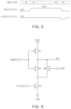
- FIG. 5 is a diagram illustrating an operation of a semiconductor device according to example embodiments of the present disclosure.
- a semiconductor device may receive a row command signal CMD_ROW from an external host such as a central processing unit, an application processor, or the like.
- a control logic of the semiconductor device may determine selected word lines and unselected word lines from among a plurality of word lines with reference to the row command signal CMD_ROW and an address signal received together with the row command signal CMD_ROW.
- the control logic may increase a voltage level of a selected word line in response to an activation command ACT (not shown) of the row command signal CMD_ROW. For example, the control logic may increase a voltage of the selected word line from an initial level Vinit to an active level Vpwr by controlling a sub-word line decoder connected to the selected word line in a word line driving circuit. Conversely, voltage levels of unselected word lines may be maintained as the initial level Vinit.
- the control logic may perform a control operation for a selected memory cell connected to the selected word line using bit line sense amplifiers while the voltage of the selected word line is maintained at the active level Vpwr.
- the control operation may include a program operation, a read operation, a refresh operation, and the like.
- a control logic circuit may control the sub-word line decoder connected to the selected word line to restore the voltage of the selected word line from the active level Vpwr to the initial level Vinit.
- At least one unselected word line, adjacent to the selected word line, among unselected word lines may be caused to float (i.e., may be floated) while the voltage of the selected word line returns to the initial level Vinit.
- a voltage of the floating unselected word line may decrease to a level lower than the initial level Vinit as illustrated in FIG. 5 , in response to a decrease in the voltage of the adjacent selected word line. Accordingly, in a memory cell including a gate structure providing an unselected word line, a cell switch may be turned off, and charges flowing into a cell capacitor may be effectively blocked, thereby minimizing data loss of an unselected memory cell.
- FIGS. 6 and 7 are schematic diagrams illustrating a sub-word line decoder included in a semiconductor device according to example embodiments of the present disclosure.
- FIG. 6 is a circuit diagram illustrating a sub-word line decoder included in a memory device according to example embodiments of the present disclosure.
- the sub-word line decoder may include a plurality of switch elements PM 1 , NM 1 , and NM 2 and at least one floating element NM 3 .
- the plurality of switch elements PM 1 , NM 1 , and NM 2 may be connected to each other in series, and may include a first switch element PM 1 being turned on and off by a word line control signal NWEIB, a second switch element NW, and a third switch element NM 2 .
- the first switch element PM 1 may be connected in series with the second and third switch elements NM 1 and NM 2 , and the second and third switch elements NM 1 and NM 2 may be connected with each other in parallel.
- the second switch element NM 1 and the third switch element NM 2 may be connected to each other in parallel.
- an element may be turned on (or similar language) when a current can flow freely therethrough.
- an element may be turned off (or similar language) when little to no current can flow therethrough (e.g., a leakage current may still exist). When an element is turned off, it may still be considered to be electrically connected to another element or between other elements, but little to no current may flow through the element.
- the first switch element PM 1 may be a PMOS transistor, and the second switch element NM 1 may be an NMOS transistor.
- a first driving signal PXID may be input into the first switch element PM 1 , and the second switch element NM 1 may be connected to the floating element NM 3 .
- the first driving signal PXID may have different levels depending on whether a word line WL connected to the sub-word line decoder is a selected word line.
- a node that has the first driving signal PXID may be a driving node, and a voltage at the driving node may be a voltage of the first driving signal PXID.
- the driving node may supply the first driving signal PXID.
- the first switch element PM 1 may be connected between the driving node and a word line WL connected to the sub-word line decoder.
- the third switch element NM 2 may be turned on and off by a second driving signal PXIB.
- the third switch element NM 2 may be connected to a reference node supplying a reference voltage VSS through the floating element NM 3 .
- the reference node may supply a voltage at an initial level.
- a voltage at the reference node may be a reference voltage VSS. Accordingly, when the floating element NM 3 is turned on, the reference voltage VSS may be input into the second switch element NM 1 and the third switch element NM 2 .
- the floating element NM 3 may be turned on and off by a floating control signal FLOATB.
- the reference voltage VSS corresponding to an initial level may be input into the word line WL.
- the word line WL may float.
- a control logic of a semiconductor device may control the plurality of switch elements PM 1 , NW, and NM 2 and the floating element NM 3 to adjust a voltage level of the word line WL or to cause the word line WL to float. For example, when the word line WL is a selected word line, the control logic may turn on the first switch element PM 1 and turn off the second switch element NM 1 and the third switch element NM 2 . In addition, a voltage of the word line WL may be increased to an active level by increasing a level of the first driving signal PXID.
- control logic may turn off the first switch element PM 1 and turn on the second switch element NM 1 and the third switch element NM 2 .
- control logic may also turn on the floating element NM 3 to input the reference voltage VSS corresponding to the initial level into the word line WL.
- the control logic may connect the word line WL to the reference node until a control operation performed on the selected memory cell is completed and a voltage of the selected word line returns to the initial level. Accordingly, the voltage of the word line WL may be continuously maintained as the reference voltage VSS.
- the control logic may be configured to set respective voltages of unselected word lines, not adjacent to the selected word line, to the initial level.
- the control logic may turn on the second switch element NM 1 and the third switch element NM 2 and turn off the first switch element PM 1 and the floating element NM 3 in at least a portion of a period in which the voltage of the selected word line returns to the initial level.
- the word line WL may float.
- the floating word line WL may decrease to a voltage at a level lower than the reference voltage VSS such that the voltage of the floating word line WL is under the influence (e.g., low enough to avoid or reduce the influence) of a precharging operation in which the voltage of the adjacent selected word line returns to the initial level, thereby effectively preventing data loss of unselected memory cells connected to the word line WL.
- FIG. 7 is a diagram illustrating a connection relationship between sub-word line decoders SWD 1 to SWD 16 and control signals.
- some sub-word line decoders adjacent to each other may be grouped into decoder groups 210 and 220 .
- each of the decoder groups 210 and 220 may include eight of the plurality of sub-word line decoders SWD 1 to SWD 16 .
- a first word line control signal NWEIB 1 may be input in common into first to eighth sub-word line decoders SWD 1 to SWD 8 of a first decoder group 210
- a second word line control signal NWEIB 2 may be input in common into ninth to sixteenth sub-word line decoders SWD 9 to SWD 16 of a second decoder group 220 .
- One of first to eighth driving signals PXIB 1 to PXIB 8 may be input in common into an i-th (i is a natural number from 1 to 8) sub-word line decoder of the first decoder group 210 and an i-th sub-word line decoder of the second decoder group 220 .
- the ninth sub-word line decoder SWD 9 may be considered a first sub-word line decoder SWD 9 of the second decoder group 220
- the tenth sub-word line decoder SWD 10 may be considered a second sub-word line decoder SWD 10 of the second decoder group 220
- the eleventh to sixteenth sub-word line decoders SWD 11 to SWD 16 may be considered in the same manner.
- each of the first to eighth driving signals PXIB 1 to PXIB 8 may be a signal input into a first switch element included in each of the sub-word line decoders SWD 1 to SWD 16 .
- the control logic can control the plurality of sub-word line decoders SWD 1 to SWD 16 depending on whether a sub-word line decoder connected to an unselected word line, adjacent to the selected word line, and a sub-word line decoder connected to the selected word line are commonly included in one of the decoder groups 210 and 220 .
- a sub-word line decoder connected to an unselected word line, adjacent to the selected word line, and a sub-word line decoder connected to the selected word line are commonly included in one of the decoder groups 210 and 220 .
- FIG. 8 is a schematic diagram illustrating a semiconductor device according to example embodiments of the present disclosure.
- FIG. 9 is a diagram illustrating an operation of a semiconductor device according to example embodiments of the present disclosure.
- a semiconductor device 300 may include a memory cell array 310 , sub-word line decoders 320 and 330 , and the like.
- the memory cell array 310 may include a plurality of memory cells MC.
- the memory cell array 310 may be connected to the sub-word line decoders 320 and 330 through a plurality of word lines WLn and WLn+1.
- each of the sub-word line decoders 320 and 330 may include first to third switch elements PM 1 , NM 1 , and NM 2 and a floating element NM 3 .
- a word line control signal NWEIB 1 may be input in common into an n-th sub-word line decoder 320 and an n+1-th sub-word line decoder 330 . Accordingly, as described above with reference to FIG.
- the n-th sub-word line decoder 320 and the n+1-th sub-word line decoder 330 may be included in the same decoder group.
- n may be a positive natural number.
- First driving signals PXID 1 and PXID 2 and second driving signals PXIB 1 and PXIB 2 , input into the n-th sub-word line decoder 320 and the n+1-th sub-word line decoder 330 may be different from floating control signals FLOATB 1 and FLOATB 2 .
- an n-th word line WLn may be determined as a selected word line, and an n+1-th word line WLn+1 may be determined as an unselected word line.
- a first driving signal PXID 1 when the word line control signal NWEIB 1 decreases from a high logic level H to a low logic level L, a first driving signal PXID 1 , input into the n-th sub-word line decoder 320 , may increase from the low logic level L to the high logic level H.
- the first switch element PM 1 may be turned on and the second switch element NM 1 may be turned off, and the first driving signal PXID 1 may be input into the n-th word line WLn. Accordingly, a voltage of the n-th word line WLn may increase from the initial level Vinit to the active level Vpwr.
- a second driving signal PXIB 1 input into the n-th sub-word line decoder 320 , may decrease from the high logic level H to the low logic level L, and the floating control signal FLOATB 1 may be maintained at the high logic level H. Accordingly, in the n-th sub-word line decoder 320 , the third switch element NM 2 may be turned off, and the floating element NM 3 may be maintained in an ON state.
- a first driving signal PXID 2 input into the n+1-th sub-word line decoder 330 , may be maintained at the low logic level L.
- a second driving signal PXIB 2 and a floating control signal FLOATB 2 input into the n+1-th sub-word line decoder 330 , may be maintained at the high logic level H.
- the reference voltage VSS may be input into the n+1-th word line WLn+1, and a voltage of the n+1-th word line WLn+1 may be maintained at an initial level corresponding to the reference voltage VSS.
- the voltage of the n-th word line WLn may decrease from the active level Vpwr to the initial level Vinit.
- the word line control signal NWEIB 1 and the second driving signal PXIB 1 may transition to the high logic level H, and the first driving signal PXID 1 may transition to the low logic level L.
- the reference voltage VSS may be input into the n-th word line WLn by the n-th sub-word line decoder 320 , and the voltage of the n-th word line WLn may decrease from the active level Vpwr to the initial level Vinit.
- the floating control signal FLOATB 2 may transition to the low logic level L at the first time point t 1 .
- a logic level of the floating control signal FLOATB 2 may be set to the low logic level L during at least a portion of a precharging period in which a voltage of the n-th word line WLn decreases from the active level Vpwr to the initial level Vinit.
- a voltage of the low logic level L may correspond to a voltage at the initial level (e.g., a reference voltage VSS).
- a voltage of the floating control signal FLOATB 2 may be set to the initial level Vinit during at least a portion of a precharging period in which a voltage of the n-th word line WLn decreases from the active level Vpwr to the initial level Vinit.
- the floating element NM 3 of the n+1-th sub-word line decoder 330 may be turned off, and the n+1-th word line WLn+1 may float.
- a second time period ⁇ T 2 in which the n+1-th word line WLn+1 floats may be longer than a first time period ⁇ T 1 in which the voltage of the n-th word line WLn decreases to the initial level Vinit.
- the first time period ⁇ T 1 may correspond to a precharging period in which a voltage of the n-th word line WLn decreases from the active level Vpwr to the initial level Vinit.
- the voltage of the n+1-th word line WLn+1 may decrease to a floating level Vft lower than the initial level Vinit. This may be because the voltage of the n-th word line WLn, adjacent to the n+1-th word line WLn+1, decreases from the active level Vpwr to the initial level Vinit.
- the voltage of the n+1-th word line WLn+1 may be set to a floating level Vft that is lower than the initial level Vinit during at least a portion of a period in which the voltage of the n-th word line WLn decreases from the active level Vpwr to the initial level Vinit.
- a second voltage difference ⁇ V 2 between the initial level Vinit and the floating level Vft may be less than a first voltage difference ⁇ V 1 between the active level Vpwr and the initial level Vinit.
- a voltage variation range (e.g., ⁇ V 1 ) of the n-th word line WLn (e.g., the selected word line) may be greater than a voltage variation range (e.g., ⁇ V 2 ) of the n+1-th word line WLn+1 (e.g., the unselected word line).
- the floating control signal FLOATB 2 input into the n+1-th sub-word line decoder 330 , may transition back to the high logic level H after the second time period ⁇ T 2 elapses, such that the floating element NM 3 may be turned on, and the voltage of the n+1-th word line WLn+1 may increase to the initial level Vinit.
- the voltage of the adjacent n+1-th word line WLn+1 may be reduced to the floating level Vft lower than the initial level Vinit, thereby preventing charges discharged from a channel region adjacent to a gate structure providing the n-th word line WLn from flowing into memory cells connected to the n+1-th word line WLn+1. Accordingly, loss and/or change of data of unselected memory cells connected to an unselected word line, adjacent to a selected word line, may be minimized.
- FIG. 10 is a schematic diagram illustrating a semiconductor device according to example embodiments of the present disclosure.
- FIGS. 11 to 13 are diagrams illustrating an operation of a semiconductor device according to example embodiments of the present disclosure.
- a semiconductor device 400 may include a memory cell array 410 , sub-word line decoders 420 and 430 , and the like.
- the memory cell array 410 may include a plurality of memory cells MC.
- the memory cell array 410 may be connected to the sub-word line decoders 420 and 430 through a plurality of word lines WLn and WLn+1.
- Each of the sub-word line decoders 420 and 430 may include first to third switch elements PM 1 , NM 1 , and NM 2 , and a floating element NM 3 .
- a first word line control signal NWEIB 1 may be input into an n-th sub-word line decoder 420
- a second word line control signal NWEIB 2 may be input into an n+1-th sub-word line decoder 430 .
- the n-th sub-word line decoder 420 and the n+1-th sub-word line decoder 430 may be grouped into different decoder groups.
- the n-th word line WLn may be determined as a selected word line, and the n+1-th word line WLn+1 may be determined as an unselected word line.
- the first driving signal PXID 1 input into the n-th sub-word line decoder 420 , may transition to the high logic level H, and the second driving signal PXIB 1 and the word line control signal NWEIB 1 may transition to the low logic level L, such that a voltage of the n-th word line WLn may increase from the initial level Vinit to the active level Vpwr.
- the first driving signal PXID 2 input into the n+1-th sub-word line decoder 430 , may be maintained at the low logic level L, and the word line control signal NWEIB 2 and the second driving signal PXIB 2 may be maintained at the high logic level H. Accordingly, a voltage of the n+1-th word line WLn+1 may be maintained at the initial level Vinit.
- the voltage of the n-th word line WLn may decrease from the active level Vpwr to the initial level Vinit during the first time period ⁇ T 1 starting from the first time point t 1 .
- the floating control signal FLOATB 2 input into the n+1-th sub-word line decoder 430 , may transition to the low logic level L at the first time point t 1 , such that the floating element NM 3 may be turned off, and the n+1-th word line WLn+1 may float from the first time point t 1 .
- a voltage of the floating control signal FLOATB 2 may be set to the initial level Vinit during at least a portion of a precharging period in which a voltage of the n-th word line WLn decreases from the active level Vpwr to the initial level Vinit. Accordingly, the voltage of the n+1-th word line WLn+1 may decrease to the floating level Vft lower than the initial level Vinit under the influence of a decrease in the voltage of the adjacent n-th word line WLn.
- the floating control signal FLOATB 2 may turn off the floating element NM 3 during the second time period ⁇ T 2 .
- the second voltage difference ⁇ V 2 between the initial level Vinit and the floating level Vft may be less than the first voltage difference ⁇ V 1 between the initial level Vinit and the active level Vpwr.
- the n+1-th word line WLn+1 may float at a second time point t 2 earlier than the first time point t 1 .
- the n+1-th word line WLn+1 may float first.
- the n+1-th word line WLn+1 may be floated during at least a portion of a period in which the voltage of the n-th word line WLn is maintained at the active level Vpwr.
- the second time period ⁇ T 2 in which the n+1-th word line WLn+1 is caused to float by the floating control signal FLOATB 2 may start earlier than the first time period ⁇ T 1 in which the voltage of the n-th word line WLn decreases from the active level Vpwr to the initial level Vinit, and may end later than the first time period ⁇ T 1 .
- the n+1-th word line WLn+1 may float at a third time point t 3 later than the first time point t 1 .
- the third time point t 3 may belong to the first time period ⁇ T 1 in which the voltage of the n-th word line WLn decreases from the active level Vpwr to the initial level Vinit.
- the floating element NM 3 of the n+1-th sub-word line decoder 430 may be turned off.
- the voltage of the n-th word line WLn may begin to decrease from the active level Vpwr to the initial level Vinit before the floating element NM 3 of the n+1-th sub-word line decoder 430 is turned off, but may not decrease entirely from the active level Vpwr to the initial level Vinit before the floating element NM 3 of the n+1-th sub-word line decoder 430 is turned off.
- a logic level of the floating control signal FLOATB 2 may be set to the high logic level H during at least a portion of a precharging period in which a voltage of the n-th word line WLn decreases from the active level Vpwr to the initial level Vinit.
- a voltage of the high logic level H may correspond to a voltage that is higher than the initial level Vinit.
- a voltage of the floating control signal FLOATB 2 may be set to a voltage higher than the initial level Vinit during at least a portion of a precharging period in which a voltage of the n-th word line WLn decreases from the active level Vpwr to the initial level Vinit. Accordingly, as illustrated in FIG. 13 , a portion of the first time period ⁇ T 1 may overlap the second time period ⁇ T 2 .
- FIGS. 14 to 16 are diagrams illustrating an operation of a semiconductor device according to example embodiments of the present disclosure.
- a control logic of a semiconductor device 500 may select the n-th word line WLn as a selected word line, and select the n+1-th word line WLn+1 as an unselected word line in a memory cell array 510 .
- the first switch element PM 1 may be turned on, and the second switch element NM 1 and the third switch element NM 2 may be turned off.
- the floating element NM 3 can be turned on by the floating control signal FLOATB 1 . However, since the second switch element NM 1 and the third switch element NM 2 are turned off, a voltage of the n-th word line WLn may be determined depending on the first driving signal PXID 1 rather than the reference voltage VSS.
- the control logic of the semiconductor device 500 may increase a level of the first driving signal PXID 1 , thereby increasing the voltage of the n-th word line WLn to an active level, and turning on the cell switch SW of each of the memory cells MC connected to the n-th word line WLn.
- the first switch element PM 1 may be turned off, the second switch element NM 1 , the third switch element NM 2 , and the floating element NM 3 may be turned on. Accordingly, the reference voltage VSS may be input into the n+1-th word line WLn+1 by the n+1-th sub-word line decoder 530 , and the cell switch SW of each of the memory cells MC connected to the n+1-th word line WLn+1 may be maintained in an OFF state.
- the control logic of the semiconductor device 500 may perform a control operation on at least one of the memory cells MC connected to the n-th word line WLn using bit line sense amplifiers. When the control operation is completed, the control logic may decrease the voltage of the n-th word line WLn.
- the first switch element PM 1 may be turned off, and the second switch element NM 1 and the third switch element NM 2 may be turned on. Accordingly, the reference voltage VSS may be input into the n-th word line WLn, and the voltage of the n-th word line WLn may be initialized to an initial level.
- the control logic may cause the n+1-th word line WLn+1, an unselected word line adjacent to the n-th word line WLn, to float while the voltage of the n-th word line WLn decreases to the initial level.
- the floating element NM 3 may be turned off by the floating control signal FLOATB 2 , and accordingly neither the reference voltage VSS nor the first driving signal PXID 2 may be input into the n+1-th word line WLn+1.
- a voltage of the n+1-th word line WLn+1 may decrease to a level lower than the initial level under the influence of a decrease in the voltage of the adjacent n-th word line WLn. Accordingly, the cell switch SW of each of the memory cells MC connected to the n+1-th word line WLn+1 may be turned off more strongly than the state described with reference to FIG.
- the cell switches SW connected to the n-th word line WLn may be turned off, and charges discharged from a channel region may not flow into the cell capacitors CC of the memory cells MC connected to the n+1-th word line WLn+1, thereby preventing change and/or loss of data of the memory cells MC connected to the unselected word line, and improving reliability of the semiconductor device 500 .
- the floating element NM 3 may be turned on by the floating control signal FLOATB 2 after a predetermined time period elapses. Accordingly, the n+1-th word line WLn+1 may be connected to the reference node, and the voltage of the n+1-th word line WLn+1 may return to the initial level.
- an unselected word line may not completely float.
- a floating element may not be completely turned off. A voltage between a turn-on voltage and a turn-off voltage may be input into the floating element, and thus the floating element may operate as a type of resistance element.
- the floating element may be connected between a reference node supplying a reference voltage and some of a plurality of switch elements. Accordingly, while the floating element operates as a resistive element, it can be seen that an equivalent circuit in which the unselected word line is connected to the reference node through the resistance element is formed, and charges of the unselected word line may be removed through the floating element.
- a resistive element it can be seen that an equivalent circuit in which the unselected word line is connected to the reference node through the resistance element is formed, and charges of the unselected word line may be removed through the floating element.
- FIGS. 17 and 18 are diagrams illustrating an operation of a semiconductor device according to example embodiments of the present disclosure.
- an intermediate voltage Vmid between a turn-on voltage and a turn-off voltage may be input into the floating element NM 3 of a sub-word line decoder 600 to which the word line WL is connected.
- the intermediate voltage Vmid may be input into the floating element NM 3 during at least a portion of a precharging period in which a voltage of the other word line returns from an active level to an initial level.
- the intermediate voltage Vmid may be input into the floating element NM 3 of the sub-word line decoder 600 .
- the floating element NM 3 may be an NMOS transistor.
- the intermediate voltage Vmid may have a level higher than the low logic level L corresponding to a turn-off voltage of the floating element NM 3 , and lower than the high logic level H corresponding to a turn-on voltage of the floating element NM 3 .
- the floating element NM 3 may operate as a type of resistance element.
- the word line control signal NWEIB the first switch element PM 1 may be turned off and the second switch element NM 1 may be turned on.
- the third switch element NM 2 may be turned on by the second driving signal PXIB. Accordingly, the word line WL may be connected to the floating element NM 3 operating as a resistance element.
- the word line WL may be connected to a reference node supplying the reference voltage VSS through the sub-word line decoder 600 (e.g., through the floating element NM 3 ), and a charge leakage path through which the leakage current I LEAK flows may be formed between the word line WL and the reference node. While a voltage of another word line, adjacent to the word line WL, decreases from the active level to the initial level, charges may be discharged from a channel region of cell switches connected to the another word line, and a parasitic capacitance component between the word line WL and the another adjacent word line may be charged due to the discharged charges.
- a path through which the leakage current I LEAK flows may be generated by weakly turning on the floating element NM 3 . Accordingly, when parasitic capacitance between word lines is charged due to charges discharged during a turn-off operation of cell switches connected to a selected word line, the parasitic capacitance may be removed using the leakage current LEAK. For example, when a specific word line is repeatedly selected as the selected word line and accesses to the word line are accumulated, a control logic of a semiconductor device may control the sub-word line decoder 600 connected to another adjacent word line, as described with reference to FIGS. 17 and 18 , thereby removing the parasitic capacitance between the word lines.
Landscapes
- Engineering & Computer Science (AREA)
- Microelectronics & Electronic Packaging (AREA)
- Computer Hardware Design (AREA)
- Dram (AREA)
- Power Engineering (AREA)
- Physics & Mathematics (AREA)
- Condensed Matter Physics & Semiconductors (AREA)
- General Physics & Mathematics (AREA)
Abstract
Description
Claims (20)
Applications Claiming Priority (2)
| Application Number | Priority Date | Filing Date | Title |
|---|---|---|---|
| KR10-2022-0115534 | 2022-09-14 | ||
| KR1020220115534A KR102748885B1 (en) | 2022-09-14 | 2022-09-14 | Semiconductor device |
Publications (2)
| Publication Number | Publication Date |
|---|---|
| US20240087640A1 US20240087640A1 (en) | 2024-03-14 |
| US12236998B2 true US12236998B2 (en) | 2025-02-25 |
Family
ID=90141567
Family Applications (1)
| Application Number | Title | Priority Date | Filing Date |
|---|---|---|---|
| US18/143,127 Active 2043-10-23 US12236998B2 (en) | 2022-09-14 | 2023-05-04 | Semiconductor device |
Country Status (3)
| Country | Link |
|---|---|
| US (1) | US12236998B2 (en) |
| KR (1) | KR102748885B1 (en) |
| CN (1) | CN117711459A (en) |
Citations (19)
| Publication number | Priority date | Publication date | Assignee | Title |
|---|---|---|---|---|
| US7180787B2 (en) | 2004-03-29 | 2007-02-20 | Kabushiki Kaisha Toshiba | Semiconductor memory device |
| US20090116304A1 (en) | 2007-11-02 | 2009-05-07 | Hynix Semiconductor Inc. | Wordline driving circuit of semiconductor memory device |
| KR101096225B1 (en) | 2008-08-21 | 2011-12-22 | 주식회사 하이닉스반도체 | Semiconductor memory device and driving method thereof |
| US20150117079A1 (en) | 2011-12-15 | 2015-04-30 | SK Hynix Inc. | Sub word line driver and semiconductor integrated circuit device |
| US20160064056A1 (en) | 2014-08-26 | 2016-03-03 | Samsung Electronics Co., Ltd. | Semiconductor memory devices and memory systems including the same |
| US9311984B1 (en) | 2014-09-23 | 2016-04-12 | SK Hynix Inc. | Smart refresh device |
| US20160133323A1 (en) | 2014-11-07 | 2016-05-12 | Samsung Electronics Co., Ltd. | Memory device and method of operating the same |
| US9653139B1 (en) | 2016-04-01 | 2017-05-16 | SK Hynix Inc. | Simultaneous plural wordline within a bank refreshing control device and memory device including the same |
| US9858982B1 (en) | 2016-10-27 | 2018-01-02 | SK Hynix Inc. | Refresh control device |
| US10192608B2 (en) | 2017-05-23 | 2019-01-29 | Micron Technology, Inc. | Apparatuses and methods for detection refresh starvation of a memory |
| US20190318784A1 (en) * | 2018-04-16 | 2019-10-17 | Samsung Electronics Co., Ltd. | Nonvolatile memory device and method of programming in the same |
| US20210027835A1 (en) | 2019-07-26 | 2021-01-28 | Samsung Electronics Co., Ltd. | Memory device for controlling unselected memory cells in accordance with adjacency to selected memory cell, and method for operating the same |
| US20210027829A1 (en) | 2019-07-25 | 2021-01-28 | Samsung Electronics Co., Ltd. | Memory device and method of operating the same |
| US20210193213A1 (en) | 2019-12-19 | 2021-06-24 | Samsung Electronics Co., Ltd. | Memory devices |
| US11062763B2 (en) | 2019-04-09 | 2021-07-13 | Micron Technology, Inc. | Memory array with multiplexed digit lines |
| US11087821B2 (en) | 2018-09-17 | 2021-08-10 | Samsung Electronics Co., Ltd. | Memory module including register clock driver detecting address frequently accessed |
| US11200943B2 (en) | 2019-11-19 | 2021-12-14 | Micron Technology, Inc. | Sub-word line driver with soft-landing |
| US20220165325A1 (en) | 2020-11-20 | 2022-05-26 | SK Hynix Inc. | Volatile memory device, storage device, and operating method of volatile memory device |
| US20220310169A1 (en) * | 2021-03-24 | 2022-09-29 | Yangtze Memory Technologies Co., Ltd. | Memory device and erase operation thereof |
-
2022
- 2022-09-14 KR KR1020220115534A patent/KR102748885B1/en active Active
-
2023
- 2023-05-04 US US18/143,127 patent/US12236998B2/en active Active
- 2023-08-08 CN CN202310989356.1A patent/CN117711459A/en active Pending
Patent Citations (22)
| Publication number | Priority date | Publication date | Assignee | Title |
|---|---|---|---|---|
| US7180787B2 (en) | 2004-03-29 | 2007-02-20 | Kabushiki Kaisha Toshiba | Semiconductor memory device |
| US20090116304A1 (en) | 2007-11-02 | 2009-05-07 | Hynix Semiconductor Inc. | Wordline driving circuit of semiconductor memory device |
| KR101096225B1 (en) | 2008-08-21 | 2011-12-22 | 주식회사 하이닉스반도체 | Semiconductor memory device and driving method thereof |
| US20150117079A1 (en) | 2011-12-15 | 2015-04-30 | SK Hynix Inc. | Sub word line driver and semiconductor integrated circuit device |
| US20160064056A1 (en) | 2014-08-26 | 2016-03-03 | Samsung Electronics Co., Ltd. | Semiconductor memory devices and memory systems including the same |
| US9311984B1 (en) | 2014-09-23 | 2016-04-12 | SK Hynix Inc. | Smart refresh device |
| US20160133323A1 (en) | 2014-11-07 | 2016-05-12 | Samsung Electronics Co., Ltd. | Memory device and method of operating the same |
| KR20160055012A (en) | 2014-11-07 | 2016-05-17 | 삼성전자주식회사 | Memory Devices and Methods of Operating the Memory Device |
| US9653139B1 (en) | 2016-04-01 | 2017-05-16 | SK Hynix Inc. | Simultaneous plural wordline within a bank refreshing control device and memory device including the same |
| US9858982B1 (en) | 2016-10-27 | 2018-01-02 | SK Hynix Inc. | Refresh control device |
| US10192608B2 (en) | 2017-05-23 | 2019-01-29 | Micron Technology, Inc. | Apparatuses and methods for detection refresh starvation of a memory |
| US20190318784A1 (en) * | 2018-04-16 | 2019-10-17 | Samsung Electronics Co., Ltd. | Nonvolatile memory device and method of programming in the same |
| US11087821B2 (en) | 2018-09-17 | 2021-08-10 | Samsung Electronics Co., Ltd. | Memory module including register clock driver detecting address frequently accessed |
| US11062763B2 (en) | 2019-04-09 | 2021-07-13 | Micron Technology, Inc. | Memory array with multiplexed digit lines |
| US20210027829A1 (en) | 2019-07-25 | 2021-01-28 | Samsung Electronics Co., Ltd. | Memory device and method of operating the same |
| KR20210013435A (en) | 2019-07-25 | 2021-02-04 | 삼성전자주식회사 | Memory device and operating method thereof |
| US20210027835A1 (en) | 2019-07-26 | 2021-01-28 | Samsung Electronics Co., Ltd. | Memory device for controlling unselected memory cells in accordance with adjacency to selected memory cell, and method for operating the same |
| US11200943B2 (en) | 2019-11-19 | 2021-12-14 | Micron Technology, Inc. | Sub-word line driver with soft-landing |
| US20210193213A1 (en) | 2019-12-19 | 2021-06-24 | Samsung Electronics Co., Ltd. | Memory devices |
| KR20210079436A (en) | 2019-12-19 | 2021-06-30 | 삼성전자주식회사 | Memory device |
| US20220165325A1 (en) | 2020-11-20 | 2022-05-26 | SK Hynix Inc. | Volatile memory device, storage device, and operating method of volatile memory device |
| US20220310169A1 (en) * | 2021-03-24 | 2022-09-29 | Yangtze Memory Technologies Co., Ltd. | Memory device and erase operation thereof |
Also Published As
| Publication number | Publication date |
|---|---|
| KR102748885B1 (en) | 2025-01-02 |
| CN117711459A (en) | 2024-03-15 |
| KR20240036915A (en) | 2024-03-21 |
| US20240087640A1 (en) | 2024-03-14 |
Similar Documents
| Publication | Publication Date | Title |
|---|---|---|
| US6980454B2 (en) | Low-power consumption semiconductor memory device | |
| US6992928B2 (en) | Semiconductor memory device with an improved memory cell structure and method of operating the same | |
| US6891742B2 (en) | Semiconductor memory device | |
| US9412432B2 (en) | Semiconductor storage device and system provided with same | |
| JP3962638B2 (en) | Semiconductor memory device and semiconductor device | |
| US9548104B1 (en) | Boost control to improve SRAM write operation | |
| US8917567B2 (en) | Semiconductor device having hierarchical bit line structure and control method thereof | |
| US7599208B2 (en) | Nonvolatile ferroelectric memory device and refresh method thereof | |
| US9990975B2 (en) | Nonvolatile semiconductor memory | |
| US5912840A (en) | Memory cell architecture utilizing a transistor having a dual access gate | |
| JP2002093154A (en) | Ferroelectric memory | |
| JP2003282823A (en) | Semiconductor integrated circuit | |
| JP5363644B2 (en) | Semiconductor device | |
| US6831866B1 (en) | Method and apparatus for read bitline clamping for gain cell DRAM devices | |
| US12236998B2 (en) | Semiconductor device | |
| US12131769B2 (en) | Sub-word line driver having common gate boosted voltage | |
| US9281042B1 (en) | Non-volatile memory using bi-directional resistive elements and capacitive elements | |
| US5563434A (en) | Semiconductor memory device having capacitor of thin film transistor structure | |
| US20250174276A1 (en) | Memory devices and operating methods thereof, memory systems, word line voltage control circuits | |
| JP2023179834A (en) | semiconductor equipment | |
| WO2024198549A1 (en) | Memory and control method for memory, and storage system and electronic device | |
| KR20250052880A (en) | Memory device and operating method thereof | |
| CN119314530A (en) | Semiconductor memory device capable of controlling row hammering and driving method thereof | |
| Chung | High performance ferroelectric memory with grounded-plate PMOS-gate cell technology | |
| JPH04228177A (en) | Semiconductor memory device |
Legal Events
| Date | Code | Title | Description |
|---|---|---|---|
| AS | Assignment |
Owner name: SAMSUNG ELECTRONICS CO., LTD., KOREA, REPUBLIC OF Free format text: ASSIGNMENT OF ASSIGNORS INTEREST;ASSIGNORS:CHO, SEONGJIN;KANG, KYUCHANG;PARK, KEONWOO;AND OTHERS;REEL/FRAME:063530/0324 Effective date: 20230327 |
|
| FEPP | Fee payment procedure |
Free format text: ENTITY STATUS SET TO UNDISCOUNTED (ORIGINAL EVENT CODE: BIG.); ENTITY STATUS OF PATENT OWNER: LARGE ENTITY |
|
| STPP | Information on status: patent application and granting procedure in general |
Free format text: DOCKETED NEW CASE - READY FOR EXAMINATION |
|
| STPP | Information on status: patent application and granting procedure in general |
Free format text: NOTICE OF ALLOWANCE MAILED -- APPLICATION RECEIVED IN OFFICE OF PUBLICATIONS |
|
| ZAAB | Notice of allowance mailed |
Free format text: ORIGINAL CODE: MN/=. |
|
| STPP | Information on status: patent application and granting procedure in general |
Free format text: AWAITING TC RESP, ISSUE FEE PAYMENT RECEIVED |
|
| STPP | Information on status: patent application and granting procedure in general |
Free format text: PUBLICATIONS -- ISSUE FEE PAYMENT VERIFIED |
|
| STCF | Information on status: patent grant |
Free format text: PATENTED CASE |