US12227828B2 - Structure for producing diamond and method for manufacturing same - Google Patents
Structure for producing diamond and method for manufacturing same Download PDFInfo
- Publication number
- US12227828B2 US12227828B2 US17/507,417 US202117507417A US12227828B2 US 12227828 B2 US12227828 B2 US 12227828B2 US 202117507417 A US202117507417 A US 202117507417A US 12227828 B2 US12227828 B2 US 12227828B2
- Authority
- US
- United States
- Prior art keywords
- thin film
- diamond
- base substrate
- producing
- substrate
- Prior art date
- Legal status (The legal status is an assumption and is not a legal conclusion. Google has not performed a legal analysis and makes no representation as to the accuracy of the status listed.)
- Active, expires
Links
Images


Classifications
-
- C—CHEMISTRY; METALLURGY
- C23—COATING METALLIC MATERIAL; COATING MATERIAL WITH METALLIC MATERIAL; CHEMICAL SURFACE TREATMENT; DIFFUSION TREATMENT OF METALLIC MATERIAL; COATING BY VACUUM EVAPORATION, BY SPUTTERING, BY ION IMPLANTATION OR BY CHEMICAL VAPOUR DEPOSITION, IN GENERAL; INHIBITING CORROSION OF METALLIC MATERIAL OR INCRUSTATION IN GENERAL
- C23C—COATING METALLIC MATERIAL; COATING MATERIAL WITH METALLIC MATERIAL; SURFACE TREATMENT OF METALLIC MATERIAL BY DIFFUSION INTO THE SURFACE, BY CHEMICAL CONVERSION OR SUBSTITUTION; COATING BY VACUUM EVAPORATION, BY SPUTTERING, BY ION IMPLANTATION OR BY CHEMICAL VAPOUR DEPOSITION, IN GENERAL
- C23C14/00—Coating by vacuum evaporation, by sputtering or by ion implantation of the coating forming material
- C23C14/06—Coating by vacuum evaporation, by sputtering or by ion implantation of the coating forming material characterised by the coating material
- C23C14/14—Metallic material, boron or silicon
-
- C—CHEMISTRY; METALLURGY
- C23—COATING METALLIC MATERIAL; COATING MATERIAL WITH METALLIC MATERIAL; CHEMICAL SURFACE TREATMENT; DIFFUSION TREATMENT OF METALLIC MATERIAL; COATING BY VACUUM EVAPORATION, BY SPUTTERING, BY ION IMPLANTATION OR BY CHEMICAL VAPOUR DEPOSITION, IN GENERAL; INHIBITING CORROSION OF METALLIC MATERIAL OR INCRUSTATION IN GENERAL
- C23C—COATING METALLIC MATERIAL; COATING MATERIAL WITH METALLIC MATERIAL; SURFACE TREATMENT OF METALLIC MATERIAL BY DIFFUSION INTO THE SURFACE, BY CHEMICAL CONVERSION OR SUBSTITUTION; COATING BY VACUUM EVAPORATION, BY SPUTTERING, BY ION IMPLANTATION OR BY CHEMICAL VAPOUR DEPOSITION, IN GENERAL
- C23C16/00—Chemical coating by decomposition of gaseous compounds, without leaving reaction products of surface material in the coating, i.e. chemical vapour deposition [CVD] processes
- C23C16/02—Pretreatment of the material to be coated
- C23C16/0272—Deposition of sub-layers, e.g. to promote the adhesion of the main coating
-
- C—CHEMISTRY; METALLURGY
- C23—COATING METALLIC MATERIAL; COATING MATERIAL WITH METALLIC MATERIAL; CHEMICAL SURFACE TREATMENT; DIFFUSION TREATMENT OF METALLIC MATERIAL; COATING BY VACUUM EVAPORATION, BY SPUTTERING, BY ION IMPLANTATION OR BY CHEMICAL VAPOUR DEPOSITION, IN GENERAL; INHIBITING CORROSION OF METALLIC MATERIAL OR INCRUSTATION IN GENERAL
- C23C—COATING METALLIC MATERIAL; COATING MATERIAL WITH METALLIC MATERIAL; SURFACE TREATMENT OF METALLIC MATERIAL BY DIFFUSION INTO THE SURFACE, BY CHEMICAL CONVERSION OR SUBSTITUTION; COATING BY VACUUM EVAPORATION, BY SPUTTERING, BY ION IMPLANTATION OR BY CHEMICAL VAPOUR DEPOSITION, IN GENERAL
- C23C16/00—Chemical coating by decomposition of gaseous compounds, without leaving reaction products of surface material in the coating, i.e. chemical vapour deposition [CVD] processes
- C23C16/22—Chemical coating by decomposition of gaseous compounds, without leaving reaction products of surface material in the coating, i.e. chemical vapour deposition [CVD] processes characterised by the deposition of inorganic material, other than metallic material
- C23C16/26—Deposition of carbon only
- C23C16/27—Diamond only
- C23C16/272—Diamond only using DC, AC or RF discharges
-
- C—CHEMISTRY; METALLURGY
- C23—COATING METALLIC MATERIAL; COATING MATERIAL WITH METALLIC MATERIAL; CHEMICAL SURFACE TREATMENT; DIFFUSION TREATMENT OF METALLIC MATERIAL; COATING BY VACUUM EVAPORATION, BY SPUTTERING, BY ION IMPLANTATION OR BY CHEMICAL VAPOUR DEPOSITION, IN GENERAL; INHIBITING CORROSION OF METALLIC MATERIAL OR INCRUSTATION IN GENERAL
- C23C—COATING METALLIC MATERIAL; COATING MATERIAL WITH METALLIC MATERIAL; SURFACE TREATMENT OF METALLIC MATERIAL BY DIFFUSION INTO THE SURFACE, BY CHEMICAL CONVERSION OR SUBSTITUTION; COATING BY VACUUM EVAPORATION, BY SPUTTERING, BY ION IMPLANTATION OR BY CHEMICAL VAPOUR DEPOSITION, IN GENERAL
- C23C16/00—Chemical coating by decomposition of gaseous compounds, without leaving reaction products of surface material in the coating, i.e. chemical vapour deposition [CVD] processes
- C23C16/22—Chemical coating by decomposition of gaseous compounds, without leaving reaction products of surface material in the coating, i.e. chemical vapour deposition [CVD] processes characterised by the deposition of inorganic material, other than metallic material
- C23C16/26—Deposition of carbon only
- C23C16/27—Diamond only
- C23C16/274—Diamond only using microwave discharges
-
- C—CHEMISTRY; METALLURGY
- C23—COATING METALLIC MATERIAL; COATING MATERIAL WITH METALLIC MATERIAL; CHEMICAL SURFACE TREATMENT; DIFFUSION TREATMENT OF METALLIC MATERIAL; COATING BY VACUUM EVAPORATION, BY SPUTTERING, BY ION IMPLANTATION OR BY CHEMICAL VAPOUR DEPOSITION, IN GENERAL; INHIBITING CORROSION OF METALLIC MATERIAL OR INCRUSTATION IN GENERAL
- C23C—COATING METALLIC MATERIAL; COATING MATERIAL WITH METALLIC MATERIAL; SURFACE TREATMENT OF METALLIC MATERIAL BY DIFFUSION INTO THE SURFACE, BY CHEMICAL CONVERSION OR SUBSTITUTION; COATING BY VACUUM EVAPORATION, BY SPUTTERING, BY ION IMPLANTATION OR BY CHEMICAL VAPOUR DEPOSITION, IN GENERAL
- C23C16/00—Chemical coating by decomposition of gaseous compounds, without leaving reaction products of surface material in the coating, i.e. chemical vapour deposition [CVD] processes
- C23C16/22—Chemical coating by decomposition of gaseous compounds, without leaving reaction products of surface material in the coating, i.e. chemical vapour deposition [CVD] processes characterised by the deposition of inorganic material, other than metallic material
- C23C16/26—Deposition of carbon only
- C23C16/27—Diamond only
- C23C16/279—Diamond only control of diamond crystallography
-
- C—CHEMISTRY; METALLURGY
- C30—CRYSTAL GROWTH
- C30B—SINGLE-CRYSTAL GROWTH; UNIDIRECTIONAL SOLIDIFICATION OF EUTECTIC MATERIAL OR UNIDIRECTIONAL DEMIXING OF EUTECTOID MATERIAL; REFINING BY ZONE-MELTING OF MATERIAL; PRODUCTION OF A HOMOGENEOUS POLYCRYSTALLINE MATERIAL WITH DEFINED STRUCTURE; SINGLE CRYSTALS OR HOMOGENEOUS POLYCRYSTALLINE MATERIAL WITH DEFINED STRUCTURE; AFTER-TREATMENT OF SINGLE CRYSTALS OR A HOMOGENEOUS POLYCRYSTALLINE MATERIAL WITH DEFINED STRUCTURE; APPARATUS THEREFOR
- C30B23/00—Single-crystal growth by condensing evaporated or sublimed materials
- C30B23/02—Epitaxial-layer growth
- C30B23/025—Epitaxial-layer growth characterised by the substrate
-
- C—CHEMISTRY; METALLURGY
- C30—CRYSTAL GROWTH
- C30B—SINGLE-CRYSTAL GROWTH; UNIDIRECTIONAL SOLIDIFICATION OF EUTECTIC MATERIAL OR UNIDIRECTIONAL DEMIXING OF EUTECTOID MATERIAL; REFINING BY ZONE-MELTING OF MATERIAL; PRODUCTION OF A HOMOGENEOUS POLYCRYSTALLINE MATERIAL WITH DEFINED STRUCTURE; SINGLE CRYSTALS OR HOMOGENEOUS POLYCRYSTALLINE MATERIAL WITH DEFINED STRUCTURE; AFTER-TREATMENT OF SINGLE CRYSTALS OR A HOMOGENEOUS POLYCRYSTALLINE MATERIAL WITH DEFINED STRUCTURE; APPARATUS THEREFOR
- C30B25/00—Single-crystal growth by chemical reaction of reactive gases, e.g. chemical vapour-deposition growth
- C30B25/02—Epitaxial-layer growth
- C30B25/18—Epitaxial-layer growth characterised by the substrate
- C30B25/183—Epitaxial-layer growth characterised by the substrate being provided with a buffer layer, e.g. a lattice matching layer
-
- C—CHEMISTRY; METALLURGY
- C30—CRYSTAL GROWTH
- C30B—SINGLE-CRYSTAL GROWTH; UNIDIRECTIONAL SOLIDIFICATION OF EUTECTIC MATERIAL OR UNIDIRECTIONAL DEMIXING OF EUTECTOID MATERIAL; REFINING BY ZONE-MELTING OF MATERIAL; PRODUCTION OF A HOMOGENEOUS POLYCRYSTALLINE MATERIAL WITH DEFINED STRUCTURE; SINGLE CRYSTALS OR HOMOGENEOUS POLYCRYSTALLINE MATERIAL WITH DEFINED STRUCTURE; AFTER-TREATMENT OF SINGLE CRYSTALS OR A HOMOGENEOUS POLYCRYSTALLINE MATERIAL WITH DEFINED STRUCTURE; APPARATUS THEREFOR
- C30B25/00—Single-crystal growth by chemical reaction of reactive gases, e.g. chemical vapour-deposition growth
- C30B25/02—Epitaxial-layer growth
- C30B25/18—Epitaxial-layer growth characterised by the substrate
- C30B25/186—Epitaxial-layer growth characterised by the substrate being specially pre-treated by, e.g. chemical or physical means
-
- C—CHEMISTRY; METALLURGY
- C30—CRYSTAL GROWTH
- C30B—SINGLE-CRYSTAL GROWTH; UNIDIRECTIONAL SOLIDIFICATION OF EUTECTIC MATERIAL OR UNIDIRECTIONAL DEMIXING OF EUTECTOID MATERIAL; REFINING BY ZONE-MELTING OF MATERIAL; PRODUCTION OF A HOMOGENEOUS POLYCRYSTALLINE MATERIAL WITH DEFINED STRUCTURE; SINGLE CRYSTALS OR HOMOGENEOUS POLYCRYSTALLINE MATERIAL WITH DEFINED STRUCTURE; AFTER-TREATMENT OF SINGLE CRYSTALS OR A HOMOGENEOUS POLYCRYSTALLINE MATERIAL WITH DEFINED STRUCTURE; APPARATUS THEREFOR
- C30B29/00—Single crystals or homogeneous polycrystalline material with defined structure characterised by the material or by their shape
- C30B29/02—Elements
- C30B29/04—Diamond
-
- C—CHEMISTRY; METALLURGY
- C30—CRYSTAL GROWTH
- C30B—SINGLE-CRYSTAL GROWTH; UNIDIRECTIONAL SOLIDIFICATION OF EUTECTIC MATERIAL OR UNIDIRECTIONAL DEMIXING OF EUTECTOID MATERIAL; REFINING BY ZONE-MELTING OF MATERIAL; PRODUCTION OF A HOMOGENEOUS POLYCRYSTALLINE MATERIAL WITH DEFINED STRUCTURE; SINGLE CRYSTALS OR HOMOGENEOUS POLYCRYSTALLINE MATERIAL WITH DEFINED STRUCTURE; AFTER-TREATMENT OF SINGLE CRYSTALS OR A HOMOGENEOUS POLYCRYSTALLINE MATERIAL WITH DEFINED STRUCTURE; APPARATUS THEREFOR
- C30B33/00—After-treatment of single crystals or homogeneous polycrystalline material with defined structure
-
- Y—GENERAL TAGGING OF NEW TECHNOLOGICAL DEVELOPMENTS; GENERAL TAGGING OF CROSS-SECTIONAL TECHNOLOGIES SPANNING OVER SEVERAL SECTIONS OF THE IPC; TECHNICAL SUBJECTS COVERED BY FORMER USPC CROSS-REFERENCE ART COLLECTIONS [XRACs] AND DIGESTS
- Y10—TECHNICAL SUBJECTS COVERED BY FORMER USPC
- Y10T—TECHNICAL SUBJECTS COVERED BY FORMER US CLASSIFICATION
- Y10T428/00—Stock material or miscellaneous articles
- Y10T428/26—Web or sheet containing structurally defined element or component, the element or component having a specified physical dimension
- Y10T428/263—Coating layer not in excess of 5 mils thick or equivalent
- Y10T428/264—Up to 3 mils
- Y10T428/265—1 mil or less
-
- Y—GENERAL TAGGING OF NEW TECHNOLOGICAL DEVELOPMENTS; GENERAL TAGGING OF CROSS-SECTIONAL TECHNOLOGIES SPANNING OVER SEVERAL SECTIONS OF THE IPC; TECHNICAL SUBJECTS COVERED BY FORMER USPC CROSS-REFERENCE ART COLLECTIONS [XRACs] AND DIGESTS
- Y10—TECHNICAL SUBJECTS COVERED BY FORMER USPC
- Y10T—TECHNICAL SUBJECTS COVERED BY FORMER US CLASSIFICATION
- Y10T428/00—Stock material or miscellaneous articles
- Y10T428/31504—Composite [nonstructural laminate]
- Y10T428/31678—Of metal
Definitions
- the present invention relates to a structure for producing diamond capable of epitaxially growing a large-sized diamond, and a method for manufacturing the structure for producing diamond.
- the present invention relates to a structure for producing diamond by chemical vapor deposition (hereinafter, simply referred to as “CVD”).
- the base material structure that enables the formation of diamond film has been studied for many years.
- single crystal Ir as a base material, it has become possible to grow single crystal diamond on it.
- Second point The difference in thermal expansion coefficient between the base material and diamond is as small as possible.
- Third point It can withstand the temperature, gas atmosphere or the like in the diamond growth environment and does not crack.
- examples of the base material include MgO, sapphire, and Si.
- MgO and sapphire meet the requirements of the first and third points, and high quality diamond can be obtained on the Ir thin film on these base materials.
- the thermal expansion coefficient of MgO is about 13.1 ⁇ 10 ⁇ 6 /° C. and the thermal expansion coefficient of sapphire is about 7.7 ⁇ 10 ⁇ 6 /° C.
- the thermal expansion coefficient of diamond is about 1.1 ⁇ 10 ⁇ 6 /° C.
- the difference in the thermal expansion coefficient between these base materials and diamond is large, and the formed diamond cannot withstand the thermal stress applied during film formation and cracks, thereby it makes difficult to increase in the size of the diamond.
- Several growth technique approaches have been reported to suppress cracks.
- the thermal expansion coefficient of Si is about 2.4 ⁇ 10 ⁇ 6 /° C., which is close to the thermal expansion coefficient of diamond and can withstand the growth environment of diamond, then the requirements of the second and third points are satisfied.
- the quality of the Ir thin film formed on Si is not good, and diamond cannot be heteroepitaxially grown on it, then the requirement of first point is not satisfied. Accordingly, a structure in which an intermediate layer is formed on Si and an Ir film is formed on the intermediate layer is being studied.
- Patent Document 1 discloses a base material for forming a single crystal diamond in which graphite is formed on single crystal Si or the like and an Ir film is formed on the graphite.
- the document describes that by providing a graphite layer on single crystal Si or the like, the stress generated between the base material and the single crystal diamond can be reduced as compared with the case where a conventional MgO seed base material is used.
- Patent Document 1 Japanese Unexamined Patent Application Publication No. 2012-001394
- the Ir thin film is more likely to be deteriorated, which may affect the quality of diamond. Further studies are needed to obtain high quality single crystal diamonds.
- an object of the present invention is to provide a structure for producing a high-quality single crystal diamond, and a method for manufacturing the structure for producing diamond.
- the present inventors have studied the growth of diamond using a thin Ir thin film. Furthermore, as described above, there are mainly three types of base materials for forming the Ir thin film, MgO, sapphire, and Si, but when these are used, the advantages and disadvantages of each must be considered. Therefore, the diamond growth process was studied so that a thin, high-quality Ir thin film could be used regardless of the material of the base material.
- the present inventors have focused on changing the process so as not to directly form an Ir thin film on the base material.
- the present inventors have realized that after forming Ir on a dummy substrate capable of forming a high-quality Ir thin film, and the obtained Ir thin film is transferred onto base substrate that has as small difference of thermal expansion coefficient as possible from diamond and can withstand the diamond growth environment.
- base substrate a base material
- graphite a base material
- the Ir thin film is heteroepitaxially grown on the base substrate or the intermediate layer, and there was a need for a relationship between the Ir thin film and the base substrate or the intermediate layer in terms of crystal structure and crystal orientation.
- the base substrate onto which the Ir thin film was transferred was completed based on the finding in the above study of the present invention that high quality diamond can be formed even when the crystal structure or crystal orientation of the Ir thin film and the base substrate are not related.
- the peak angle in the XRD diffraction pattern is deviated between the crystal lattice of the Ir thin film and the crystal lattice of the base substrate located directly under the Ir thin film, a better diamond can be formed.
- the Ir thin film is transferred onto the base substrate as in the present invention, high quality diamond is formed without providing an intermediate layer.
- a structure for producing a diamond composed of a base substrate and an Ir thin film formed on the base substrate
- thermal expansion coefficient of the base substrate is 5 times or less of the thermal expansion coefficient of diamond
- the melting point of the base substrate is 700° C. or higher.
- the peak angle in the X-ray diffraction pattern of the Ir thin film is different from the peak angle in the X-ray diffraction pattern of the base substrate.
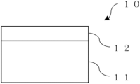
- FIG. 1 is a cross section of the structure according to the present invention.
- FIG. 2 is a schematic view of a structure in which an Ir thin film is formed on a base substrate.
- FIG. 2 A is a schematic view of a structure in which an Ir thin film is heteroepitaxially grown on a base substrate.
- FIG. 2 B is a schematic view of a structure in which an Ir thin film is transferred onto a base substrate.
- FIG. 3 is a process chart showing an example of a method for manufacturing a structure according to the present invention.
- FIG. 3 A is a perspective view showing a dummy substrate of MgO.
- FIG. 3 B is a perspective view in which an Ir thin film is formed on MgO.
- FIG. 3 C is a perspective view in which MgO on which an Ir thin film is formed is mounted on a Si substrate and bonded.
- FIG. 3 D is a perspective view showing a structure after polishing MgO after bonding.
- FIG. 4 shows a diagram showing the results of measuring the XRD rocking curve of the Ir thin film formed on the MgO substrate.
- FIG. 4 A and FIG. 4 B are diagrams showing the results of measuring the XRD rocking curve of Ir thin films each formed under different film forming conditions.
- FIG. 5 is a diagram showing an XRD diffraction pattern during the production of the structure according to the present invention.
- FIG. 5 A and FIG. 5 B are diagrams showing an XRD diffraction pattern during the removal of MgO by polishing.
- FIG. 5 C is a diagram showing an XRD diffraction pattern after polishing of MgO is completed.
- FIG. 6 is a diagram showing an XRD diffraction pattern of diamond, Ir, and MgO when diamond is heteroepitaxially grown on a structure in which an Ir thin film is heteroepitaxially grown on an MgO substrate.
- a structure for producing a diamond according to the present invention is composed of a base substrate 11 and an Ir thin film 12 formed on the base substrate 11 as shown in FIG. 1 .
- the base substrate 11 and the Ir thin film 12 of the present invention is described in more detail below.
- the base substrate 11 of the present invention needs to have a thermal expansion coefficient of 5 times or less of the thermal expansion coefficient of diamond and a melting point of 700° C. or higher. Because diamond is formed at a high temperature of at least 700° C. or higher, the melting point of the base substrate 11 on which the Ir thin film 12 is formed needs to be 700° C. or higher, preferably 800° C. or higher, more preferably 1000° C. or higher.
- the thermal expansion coefficient of the base substrate 11 of the present invention needs to be 5 times or less of the thermal expansion coefficient of diamond.
- the thermal expansion coefficient of the base substrate 11 of the present invention is 3 times or less of the thermal expansion coefficient of diamond.
- the lower limit is not particularly limited, but the thermal expansion coefficient of the base substrate 11 of the present invention is preferably 0.125 times or more, more preferably 0.2 times or more, and even more preferably 0.33 times or more of the thermal expansion coefficient of diamond.
- Examples of the base substrate 11 satisfying these requirements include Si and diamond.
- the diameter must be small-diameter because there is no large-diameter diamond that is a single crystal formed by high-temperature and high-pressure synthesis.
- a diamond different from the diamond obtained by the structure according to the present invention such as polycrystalline or sintered, can be used.
- the thermal expansion coefficient of Ir is slightly larger than the thermal expansion coefficient of diamond or Si, this does not affect the quality of diamond, so diamond or Si may be used in the present invention.
- the thermal expansion coefficient of MgO and sapphire is too large compared to the thermal expansion coefficient of diamond, the quality of diamond deteriorates even when the crystal structure and crystal orientation are not related between MgO or sapphire and the Ir thin film.
- the base substrate 11 is preferably Si.
- the thickness of the base substrate 11 may be about 0.01 to 15 mm as long as it is a normal thickness used for forming diamond.
- the size of the diameter is not particularly limited, but 0.5 inch or more is desirable.
- the Ir thin film 12 of the present invention is not epitaxially grown on the base substrate 11 , but is formed by transferring a film formed on a dummy substrate, which will be described later, onto the base substrate 11 . Therefore, the peak angle in the XRD diffraction pattern is deviated between the base substrate 11 and the Ir thin film 12 , and the crystal structure and the crystal orientation is not related unlike the case where the film is formed by epitaxial growth.
- the fact that the crystal structure and crystal orientation of the Ir thin film 12 and the base substrate 11 are not related is represented by that the peak angle in the X-ray diffraction pattern of the Ir thin film 12 is different from the peak angle in the X-ray diffraction pattern of the base substrate 11 .
- FIG. 2 is a schematic view of a structure in which an Ir thin film 22 is formed on a base substrate 21 .
- FIG. 2 A is a schematic view of a structure 20 in which an Ir thin film 22 is heteroepitaxially grown on a base substrate 21 .
- FIG. 2 B is a schematic view of a structure 30 in which an Ir thin film 32 is transferred onto a base substrate 31 .
- the Ir thin film 22 heteroepitaxially grown on the base substrate 21 grows in the same orientation as the crystal orientation of the base substrate 21 . Furthermore, the crystal structure of the Ir thin film 22 depends on the base substrate 21 . Therefore, the XRD diffraction patterns of the base substrate 21 and the Ir thin film 22 show the same peak angle.
- FIG. 2 B because the Ir thin film 32 transferred onto the base substrate 31 is grown on a dummy substrate different from the base substrate 31 , the transferred Ir thin film 32 and the base substrate 31 have different crystal structures and crystal orientations, thereby the peak angles of the XRD diffraction patterns is deviated. More specifically, all the peak angles measured by the XRD diffraction pattern of the Ir thin film 32 deviate from the peak angles of the base substrate 31 .
- the peak angle may deviate.
- only a predetermined peak may deviate, however not all the peak angles measured deviate unlike in the structure according to the present invention.
- the deviation of the peak angle in the structure according to the present invention is due to the deviation of the crystal structure and the crystal orientation, and can be easily distinguished from the deviation of the peak angle due to the defect in heteroepitaxial growth.
- a deviation in peak angle may be observed at all peaks. For example, this is the case when a cubic film is formed on a hexagonal substrate.
- the deviation of the peak angle in this case is a unique value that can be calculated from the lattice constant. Therefore, unlike the structure according to the present invention, all peak angles do not shift randomly.
- the Ir thin film 12 of the present invention shown in FIG. 1 has a quality capable of forming diamond regardless of the base substrate 11 .
- the rocking curve data measured by XRD can be used as one of the indexes for evaluating the quality of the Ir thin film 12 .
- the full width at half maximum of the (002) plane in the rocking curve of the Ir thin film 12 is 700 arcsec or less.
- the reason for paying attention to the rocking curve of the (002) plane in the Ir thin film is as follows.
- the Ir thin film also needs to have a (001) orientation in order to produce a diamond whose main surface is a (001) plane. Therefore, it is needed to investigate whether the Ir thin film exists with the (001) plane as the main plane.
- the measurement is performed on the (002) plane or the (004) plane.
- the full width at half maximum of the (002) plane is more preferably 650 arcsec or less, and more preferably 550 arcsec or less.
- the lower limit is not particularly limited, but it is preferable that the XRC full width at half maximum is small, and the XRC full width at half maximum may be equal to the inherent half width determined by the XRD radiation source.
- the XRC full width at half maximum may be 30 arcsec or more.
- the film thickness of the Ir thin film 12 of the present invention may be 5 ⁇ m or less.
- a thick Ir thin film has to be formed on a dummy substrate having a large difference in thermal expansion coefficient from diamond. It has been said that the Ir thin film needs to have a film thickness of 400 ⁇ m or more in order to suppress the warp generated during cooling after the diamond is formed.
- the base substrate 11 having a small difference in thermal expansion coefficient from that of diamond can be used, high quality diamond can be formed even if the film thickness of the Ir thin film 12 is 5 ⁇ m or less.
- the film thickness of the Ir thin film 12 is preferably 5 ⁇ m or less, more preferably 1 ⁇ m or less, and even more preferably 0.5 ⁇ m or less.
- the lower limit of the film thickness of the Ir thin film 12 is not particularly limited, but the minimum film thickness that functions as a diamond seed base material may be 0.0005 ⁇ m or more.
- the Ir thin film 12 of the present invention may be either a single crystal or a polycrystal.
- the surface of the Ir thin film 12 of the present invention is a polished surface. Therefore, high-quality diamond having extremely low surface roughness can be formed.
- the method for manufacturing a structure according to the present invention is a method for manufacturing a structure above according to the present invention.
- FIG. 3 is a process chart showing an example of a method for manufacturing a structure according to the present invention.
- FIG. 3 A is a perspective view showing a dummy substrate of MgO.
- FIG. 3 B is a perspective view in which an Ir thin film is formed on MgO.
- FIG. 3 C is a perspective view in which MgO on which an Ir thin film is formed is mounted on a Si substrate and bonded.
- FIG. 3 D is a perspective view showing a structure after polishing MgO after bonding.
- the dummy substrate is not limited to MgO
- the base substrate is not limited to Si, which are merely examples. It will be described in detail with reference to FIG. 3 .
- a dummy substrate capable of forming a high-quality Ir thin film is prepared.
- the dummy substrate is preferably one that does not melt at about 700° C., which is the heating temperature for forming Ir, and may have a melting point of 700° C. or higher.
- the upper limit of the melting point of the dummy substrate is not particularly limited, but may be about 4000° C.
- MgO or sapphire can be mentioned. From the viewpoint of producing diamond that is the purpose of producing at low cost, MgO is preferable.
- the surface roughness of the dummy substrate may be such that the Ir thin film can be formed so as to have a quality that does not deteriorate the quality of diamond.
- Ra that is arithmetic mean roughness
- of the dummy substrate may be 5 nm or less, more preferably 1 nm or less, and further preferably 0.5 nm or less.
- the lower limit of Ra of the dummy substrate is not particularly limited, but may be 0.01 nm or more.
- an Ir thin film is formed on the dummy substrate.
- a conventional method using a sputter method may be used for a method for forming an Ir thin film.
- it may be heteroepitaxially grown using DC sputtering method, RF magnetron sputtering method or the like.
- the film may be formed, for example, at an film formation temperature of 700 to 1300° C., and an under Ar gas atmosphere of about 1 ⁇ 10 ⁇ 1 to 1 ⁇ 10 ⁇ 5 Torr.
- the formed Ir thin film is transferred onto the base substrate.
- a dummy substrate is mounted onto the base substrate so that the formed Ir thin film and the beforehand-prepared base substrate are in contact with each other. Furthermore, since the base substrate is the same as that described in the above-mentioned diamond forming structure, the description thereof will be omitted.
- the Ir thin film is bonded to the base substrate. They are bonded, for example, at a heating temperature of 100 to 300° C., with a pressing force for the dummy substrate of 0.1 to 10 MPa, and with a heating time of 10 to 120 minutes.
- the atmosphere may be a vacuum of about 0.1 to 100 Torr.
- MgO which is a dummy substrate
- a high quality Ir thin film can be formed on Si.
- it may be removed by polishing or the like. It is preferable to polish to the extent that the peak derived from MgO is not measured by XRD. In this case, the Ir thin film is also slightly polished, but it is sufficient that the film thickness on which the diamond can be formed remains.
- heteroepitaxial growth is mainly carried out on an Ir thin film by CVD to form a film. It may be either microwave CVD or DC plasma CVD.
- the film formation temperature may be about 700 to 1200° C.
- a high-quality Ir thin film is provided on a base substrate having a small difference in thermal expansion coefficient from diamond. This is a configuration that could not be achieved by the conventional step of epitaxially growing an Ir thin film on a base substrate. This makes it possible to produce large-diameter, high quality diamonds.
- the structure according to the present invention does not need to have an intermediate layer interposed between the base substrate and the Ir thin film unlike in the conventional case, in the method for manufacturing a structure according to the present invention, diamond can be produced at low cost while shortening the production time.
- a 10 mm square MgO substrate capable of forming a high-quality Ir thin film was prepared, and an Ir thin film having a film thickness of 450 nm was formed.
- the sample was made using DC sputtering whose target is Ir, and the film forming conditions were Ar gas of 3 ⁇ 10 ⁇ 3 Torr and MgO temperature in the range of 1100 to 1200° C.
- the XRD rocking curve data was measured using the X'Pert-PRO MRD system (CuK ⁇ ray) manufactured by PANalytical.
- FIG. 4 shows a diagram showing the results of measuring the XRD rocking curve of the Ir thin film formed on the MgO substrate.
- FIG. 4 A and FIG. 4 B are diagrams showing the results of measuring the XRD rocking curve of Ir thin films each formed under different film forming conditions. The result of forming a film under the first condition above is shown in FIG. 4 A , and the result of forming a film under the second condition above is shown in FIG. 4 B . As shown in FIG. 4 , under each film forming condition, all the full width at half maximum of the (002) plane in the rocking curve were 700 arcsec or less. Therefore, it is considered that each Ir thin film can form a high quality diamond.
- each MgO substrate on which the Ir thin film was formed was mounted on the Si substrate beforehand-prepared so that the Ir thin film was in contact with the Si substrate.
- the Ir thin film and the Si substrate were bonded in a vacuum atmosphere having a heating temperature of 250° C., a heating time of 60 minutes, and 7.5 Torr. At this time, a pressure of 1 MPa was applied to MgO.
- FIG. 5 is a diagram showing an XRD diffraction pattern during the production of the structure according to the present invention.
- FIG. 5 A and FIG. 5 B are diagrams showing an XRD diffraction pattern during the removal of MgO by polishing.
- FIG. 5 C is a diagram showing an XRD diffraction pattern after polishing of MgO is completed.
- the apparatus used for the measurement in FIG. 5 was the same as the XRD diffractometer used for the measurement in FIG. 4 , and the measurement was performed by the ⁇ /2 ⁇ method.
- FIG. 6 is a diagram showing an XRD diffraction pattern of diamond, Ir, and MgO when diamond is heteroepitaxially grown on a structure in which an Ir thin film is heteroepitaxially grown on an MgO substrate.
- the diffraction plane of the Heteroepitaxial diamond is the (111) plane
- the diffraction plane of the Heteroepitaxial iridium is the (111) plane
- the diffraction plane of the MgO substrate is the (111) plane.
Landscapes
- Chemical & Material Sciences (AREA)
- Engineering & Computer Science (AREA)
- Materials Engineering (AREA)
- Metallurgy (AREA)
- Organic Chemistry (AREA)
- Crystallography & Structural Chemistry (AREA)
- Chemical Kinetics & Catalysis (AREA)
- General Chemical & Material Sciences (AREA)
- Mechanical Engineering (AREA)
- Inorganic Chemistry (AREA)
- Crystals, And After-Treatments Of Crystals (AREA)
Abstract
Description
-
- 10, 20, 30 structure
- 11, 21, 31 base substrate
- 12, 22, 32 Ir thin film
Claims (8)
Priority Applications (1)
| Application Number | Priority Date | Filing Date | Title |
|---|---|---|---|
| US19/015,943 US20250146122A1 (en) | 2020-10-22 | 2025-01-10 | Structure for Producing Diamond and Method for Manufacturing Same |
Applications Claiming Priority (2)
| Application Number | Priority Date | Filing Date | Title |
|---|---|---|---|
| JP2020-177489 | 2020-10-22 | ||
| JP2020177489 | 2020-10-22 |
Related Child Applications (1)
| Application Number | Title | Priority Date | Filing Date |
|---|---|---|---|
| US19/015,943 Division US20250146122A1 (en) | 2020-10-22 | 2025-01-10 | Structure for Producing Diamond and Method for Manufacturing Same |
Publications (2)
| Publication Number | Publication Date |
|---|---|
| US20220127719A1 US20220127719A1 (en) | 2022-04-28 |
| US12227828B2 true US12227828B2 (en) | 2025-02-18 |
Family
ID=80469005
Family Applications (2)
| Application Number | Title | Priority Date | Filing Date |
|---|---|---|---|
| US17/507,417 Active 2042-12-16 US12227828B2 (en) | 2020-10-22 | 2021-10-21 | Structure for producing diamond and method for manufacturing same |
| US19/015,943 Pending US20250146122A1 (en) | 2020-10-22 | 2025-01-10 | Structure for Producing Diamond and Method for Manufacturing Same |
Family Applications After (1)
| Application Number | Title | Priority Date | Filing Date |
|---|---|---|---|
| US19/015,943 Pending US20250146122A1 (en) | 2020-10-22 | 2025-01-10 | Structure for Producing Diamond and Method for Manufacturing Same |
Country Status (4)
| Country | Link |
|---|---|
| US (2) | US12227828B2 (en) |
| JP (1) | JP6998634B1 (en) |
| CN (1) | CN114381802B (en) |
| DE (1) | DE102021127590A1 (en) |
Families Citing this family (1)
| Publication number | Priority date | Publication date | Assignee | Title |
|---|---|---|---|---|
| JP7810099B2 (en) | 2022-11-29 | 2026-02-03 | 信越半導体株式会社 | Method for manufacturing heteroepitaxial substrate |
Citations (4)
| Publication number | Priority date | Publication date | Assignee | Title |
|---|---|---|---|---|
| DE19631107A1 (en) | 1995-08-04 | 1997-02-06 | Kobe Steel Ltd | Process for forming a single crystal diamond film |
| CN101892521A (en) | 2009-05-20 | 2010-11-24 | 信越化学工业株式会社 | Substrate for growing single crystal diamond layer and method for manufacturing single crystal diamond substrate |
| JP2012001394A (en) * | 2010-06-17 | 2012-01-05 | Kanazawa Univ | Substrate for growing single crystal diamond, and method for producing the single crystal diamond |
| US20160208413A1 (en) * | 2015-01-19 | 2016-07-21 | Fraunhofer-Gesellschaft zur Förderung der angewandten Forschung e.V. | Epitaxial diamond layer and method for the production thereof |
Family Cites Families (7)
| Publication number | Priority date | Publication date | Assignee | Title |
|---|---|---|---|---|
| JP4114709B2 (en) * | 1996-09-05 | 2008-07-09 | 株式会社神戸製鋼所 | Diamond film formation method |
| JP5066651B2 (en) * | 2006-03-31 | 2012-11-07 | 今井 淑夫 | Epitaxial diamond film base substrate manufacturing method and epitaxial diamond film manufacturing method using this base substrate |
| WO2018012529A1 (en) * | 2016-07-14 | 2018-01-18 | 並木精密宝石株式会社 | Single-crystal diamond substrate |
| JP6773635B2 (en) * | 2017-12-18 | 2020-10-21 | 日本電信電話株式会社 | Crystal growth method and crystal laminated structure |
| JP7077798B2 (en) * | 2018-06-11 | 2022-05-31 | 日本電信電話株式会社 | Mechanical oscillator and its manufacturing method |
| CN108707965A (en) * | 2018-06-15 | 2018-10-26 | 西安碳星半导体科技有限公司 | A kind of structure and preparation method of CVD single-crystal diamonds hetero-epitaxy substrate |
| JP2020073447A (en) * | 2020-01-21 | 2020-05-14 | 信越化学工業株式会社 | Diamond substrate and diamond freestanding substrate |
-
2021
- 2021-10-21 JP JP2021172216A patent/JP6998634B1/en active Active
- 2021-10-21 US US17/507,417 patent/US12227828B2/en active Active
- 2021-10-22 DE DE102021127590.3A patent/DE102021127590A1/en active Pending
- 2021-10-22 CN CN202111232202.5A patent/CN114381802B/en active Active
-
2025
- 2025-01-10 US US19/015,943 patent/US20250146122A1/en active Pending
Patent Citations (9)
| Publication number | Priority date | Publication date | Assignee | Title |
|---|---|---|---|---|
| DE19631107A1 (en) | 1995-08-04 | 1997-02-06 | Kobe Steel Ltd | Process for forming a single crystal diamond film |
| US5743957A (en) * | 1995-08-04 | 1998-04-28 | Kabushiki Kaisha Kobe Seiko Sho | Method for forming a single crystal diamond film |
| CN101892521A (en) | 2009-05-20 | 2010-11-24 | 信越化学工业株式会社 | Substrate for growing single crystal diamond layer and method for manufacturing single crystal diamond substrate |
| US20100294196A1 (en) * | 2009-05-20 | 2010-11-25 | Shin-Etsu Chemical Co., Ltd. | Substrate for growing single crystal diamond layer and method for producing single crystal diamond substrate |
| US9076653B2 (en) | 2009-05-20 | 2015-07-07 | Shin-Etsu Chemical Co., Ltd. | Substrate for growing single crystal diamond layer and method for producing single crystal diamond substrate |
| JP2012001394A (en) * | 2010-06-17 | 2012-01-05 | Kanazawa Univ | Substrate for growing single crystal diamond, and method for producing the single crystal diamond |
| US20160208413A1 (en) * | 2015-01-19 | 2016-07-21 | Fraunhofer-Gesellschaft zur Förderung der angewandten Forschung e.V. | Epitaxial diamond layer and method for the production thereof |
| DE102015200692A1 (en) | 2015-01-19 | 2016-07-21 | Fraunhofer-Gesellschaft zur Förderung der angewandten Forschung e.V. | Epitaxial diamond layer and process for its preparation |
| US9988737B2 (en) | 2015-01-19 | 2018-06-05 | Fraunhofer-Gesellschaft zur Förderung der angewandten Forschung e.V. | Epitaxial diamond layer and method for the production thereof |
Non-Patent Citations (1)
| Title |
|---|
| Ohtsuka et al., "Epitaxial Growth of Diamond on Iridium", Jpn. J. Appl. Phys., 1996, pp. 1072-1074, vol. 35. |
Also Published As
| Publication number | Publication date |
|---|---|
| US20250146122A1 (en) | 2025-05-08 |
| JP2022068862A (en) | 2022-05-10 |
| JP6998634B1 (en) | 2022-01-18 |
| DE102021127590A1 (en) | 2022-04-28 |
| US20220127719A1 (en) | 2022-04-28 |
| CN114381802B (en) | 2023-04-07 |
| CN114381802A (en) | 2022-04-22 |
Similar Documents
| Publication | Publication Date | Title |
|---|---|---|
| EP2524979B1 (en) | Single-crystal substrate and process for produicng group iii element nitride crystal | |
| US10619267B2 (en) | Diamond substrate | |
| JP7475389B2 (en) | Multilayer substrate, method for manufacturing multilayer substrate, and method for manufacturing free-standing substrate | |
| US20250146122A1 (en) | Structure for Producing Diamond and Method for Manufacturing Same | |
| JP7410009B2 (en) | semiconductor film | |
| JP7161158B2 (en) | Method for manufacturing diamond substrate layer | |
| US20260076191A1 (en) | Laminated substrate | |
| JP2001294499A (en) | Silicon carbide single crystal wafer with small mosaic | |
| JP2024500584A (en) | Method for growing high-quality heteroepitaxial monoclinic gallium oxide crystals | |
| WO2018216657A1 (en) | Sic wafer production method, epitaxial wafer production method, and epitaxial wafer | |
| US20240279842A1 (en) | Diamond substrate and method for manufacturing same | |
| US20170239772A1 (en) | Ramo4 substrate and manufacturing method thereof | |
| US20260009159A1 (en) | AlN SINGLE CRYSTAL SUBSTRATE AND DEVICE | |
| US10350725B2 (en) | RAMO4 substrate and manufacturing method thereof | |
| US20180190774A1 (en) | Diamond substrate and method for producing the same | |
| US11370076B2 (en) | RAMO4 substrate and manufacturing method thereof | |
| JP2019178065A (en) | Production method of single crystal diamond | |
| CN118234899A (en) | AlN single crystal substrate | |
| KR101474373B1 (en) | Semiconductor substrate and method of manufacturing the same | |
| JP2025185079A (en) | Composite substrate and device | |
| CN120363356A (en) | Recycling method of incomplete silicon carbide wafer | |
| JP2022168623A (en) | Manufacturing method of substrate of single crystal diamond and substrate of single crystal diamond | |
| JPH0750254A (en) | Method and apparatus for manufacturing semiconductor epitaxial wafer |
Legal Events
| Date | Code | Title | Description |
|---|---|---|---|
| AS | Assignment |
Owner name: DISCO CORPORATION, JAPAN Free format text: ASSIGNMENT OF ASSIGNORS INTEREST;ASSIGNORS:AIDA, HIDEO;SAWABE, ATSUHITO;KIMURA, YUTAKA;AND OTHERS;SIGNING DATES FROM 20211011 TO 20211021;REEL/FRAME:057868/0705 Owner name: WASEDA UNIVERSITY, JAPAN Free format text: ASSIGNMENT OF ASSIGNORS INTEREST;ASSIGNORS:AIDA, HIDEO;SAWABE, ATSUHITO;KIMURA, YUTAKA;AND OTHERS;SIGNING DATES FROM 20211011 TO 20211021;REEL/FRAME:057868/0705 Owner name: KIMURA, YUTAKA, JAPAN Free format text: ASSIGNMENT OF ASSIGNORS INTEREST;ASSIGNORS:AIDA, HIDEO;SAWABE, ATSUHITO;KIMURA, YUTAKA;AND OTHERS;SIGNING DATES FROM 20211011 TO 20211021;REEL/FRAME:057868/0705 Owner name: SAWABE, ATSUHITO, JAPAN Free format text: ASSIGNMENT OF ASSIGNORS INTEREST;ASSIGNORS:AIDA, HIDEO;SAWABE, ATSUHITO;KIMURA, YUTAKA;AND OTHERS;SIGNING DATES FROM 20211011 TO 20211021;REEL/FRAME:057868/0705 Owner name: NATIONAL UNIVERSITY CORPORATION NAGAOKA UNIVERSITY OF TECHNOLOGY, JAPAN Free format text: ASSIGNMENT OF ASSIGNORS INTEREST;ASSIGNORS:AIDA, HIDEO;SAWABE, ATSUHITO;KIMURA, YUTAKA;AND OTHERS;SIGNING DATES FROM 20211011 TO 20211021;REEL/FRAME:057868/0705 |
|
| FEPP | Fee payment procedure |
Free format text: ENTITY STATUS SET TO UNDISCOUNTED (ORIGINAL EVENT CODE: BIG.); ENTITY STATUS OF PATENT OWNER: LARGE ENTITY |
|
| STPP | Information on status: patent application and granting procedure in general |
Free format text: DOCKETED NEW CASE - READY FOR EXAMINATION |
|
| STPP | Information on status: patent application and granting procedure in general |
Free format text: NON FINAL ACTION MAILED |
|
| STPP | Information on status: patent application and granting procedure in general |
Free format text: RESPONSE TO NON-FINAL OFFICE ACTION ENTERED AND FORWARDED TO EXAMINER |
|
| STPP | Information on status: patent application and granting procedure in general |
Free format text: FINAL REJECTION MAILED |
|
| STPP | Information on status: patent application and granting procedure in general |
Free format text: NOTICE OF ALLOWANCE MAILED -- APPLICATION RECEIVED IN OFFICE OF PUBLICATIONS |
|
| STPP | Information on status: patent application and granting procedure in general |
Free format text: PUBLICATIONS -- ISSUE FEE PAYMENT VERIFIED |
|
| STCF | Information on status: patent grant |
Free format text: PATENTED CASE |