US12212072B2 - Antenna system - Google Patents
Antenna system Download PDFInfo
- Publication number
- US12212072B2 US12212072B2 US18/067,739 US202218067739A US12212072B2 US 12212072 B2 US12212072 B2 US 12212072B2 US 202218067739 A US202218067739 A US 202218067739A US 12212072 B2 US12212072 B2 US 12212072B2
- Authority
- US
- United States
- Prior art keywords
- antenna
- gap
- inverted
- asymmetrical
- impedance transformation
- Prior art date
- Legal status (The legal status is an assumption and is not a legal conclusion. Google has not performed a legal analysis and makes no representation as to the accuracy of the status listed.)
- Active, expires
Links
Images


Classifications
-
- H—ELECTRICITY
- H01—ELECTRIC ELEMENTS
- H01Q—ANTENNAS, i.e. RADIO AERIALS
- H01Q21/00—Antenna arrays or systems
- H01Q21/28—Combinations of substantially independent non-interacting antenna units or systems
-
- H—ELECTRICITY
- H01—ELECTRIC ELEMENTS
- H01Q—ANTENNAS, i.e. RADIO AERIALS
- H01Q1/00—Details of, or arrangements associated with, antennas
- H01Q1/12—Supports; Mounting means
- H01Q1/22—Supports; Mounting means by structural association with other equipment or articles
- H01Q1/2291—Supports; Mounting means by structural association with other equipment or articles used in bluetooth or WI-FI devices of Wireless Local Area Networks [WLAN]
-
- H—ELECTRICITY
- H01—ELECTRIC ELEMENTS
- H01Q—ANTENNAS, i.e. RADIO AERIALS
- H01Q1/00—Details of, or arrangements associated with, antennas
- H01Q1/52—Means for reducing coupling between antennas; Means for reducing coupling between an antenna and another structure
- H01Q1/521—Means for reducing coupling between antennas; Means for reducing coupling between an antenna and another structure reducing the coupling between adjacent antennas
-
- H—ELECTRICITY
- H01—ELECTRIC ELEMENTS
- H01Q—ANTENNAS, i.e. RADIO AERIALS
- H01Q5/00—Arrangements for simultaneous operation of antennas on two or more different wavebands, e.g. dual-band or multi-band arrangements
- H01Q5/30—Arrangements for providing operation on different wavebands
- H01Q5/307—Individual or coupled radiating elements, each element being fed in an unspecified way
- H01Q5/342—Individual or coupled radiating elements, each element being fed in an unspecified way for different propagation modes
- H01Q5/357—Individual or coupled radiating elements, each element being fed in an unspecified way for different propagation modes using a single feed point
- H01Q5/364—Creating multiple current paths
- H01Q5/371—Branching current paths
-
- H—ELECTRICITY
- H01—ELECTRIC ELEMENTS
- H01Q—ANTENNAS, i.e. RADIO AERIALS
- H01Q5/00—Arrangements for simultaneous operation of antennas on two or more different wavebands, e.g. dual-band or multi-band arrangements
- H01Q5/30—Arrangements for providing operation on different wavebands
- H01Q5/378—Combination of fed elements with parasitic elements
-
- H—ELECTRICITY
- H01—ELECTRIC ELEMENTS
- H01Q—ANTENNAS, i.e. RADIO AERIALS
- H01Q9/00—Electrically-short antennas having dimensions not more than twice the operating wavelength and consisting of conductive active radiating elements
- H01Q9/04—Resonant antennas
- H01Q9/0407—Substantially flat resonant element parallel to ground plane, e.g. patch antenna
- H01Q9/0421—Substantially flat resonant element parallel to ground plane, e.g. patch antenna with a shorting wall or a shorting pin at one end of the element
-
- H—ELECTRICITY
- H01—ELECTRIC ELEMENTS
- H01Q—ANTENNAS, i.e. RADIO AERIALS
- H01Q9/00—Electrically-short antennas having dimensions not more than twice the operating wavelength and consisting of conductive active radiating elements
- H01Q9/04—Resonant antennas
- H01Q9/30—Resonant antennas with feed to end of elongated active element, e.g. unipole
Definitions
- the present invention relates to systems, and more particularly, an antenna system.
- an antenna is a combination of one or more conductors.
- the antenna is the interface between radio waves propagating through space and electric currents moving in metal conductors.
- the present disclosure provides an antenna system, to solve or circumvent aforesaid problems and disadvantages in the related art.
- An embodiment of the present disclosure is related to an antenna system, and the antenna system includes a defective ground structure board and an antenna structure board.
- the defective ground structure board includes a first insulating plate and a defective ground structure layer, and the defective ground structure layer is disposed on the first insulating plate.
- the antenna structure board is disposed on the defective ground structure board, the antenna structure board includes at least one antenna body and a second insulating plate, the at least one antenna body is disposed on the second insulating plate, and the second insulating plate is disposed on the defective on the ground structure layer.
- the defective ground structure board further includes a ground layer, the ground layer is disposed under the first insulating plate, and the first insulating plate is disposed between the defective ground structure layer and the ground layer.
- the at least one antenna body has a signal feed point, a first via and a second via, and the first via and the second via respectively penetrate through the second insulating plate, the defective ground structure layer and the first insulating plate for connecting the ground layer.
- the at least one antenna body includes an inverted-F antenna and an asymmetrical T-structure component.
- the inverted-F antenna has the signal feed point and the first via.
- the asymmetrical T-structure component has the second via, the asymmetrical T-structure component is positioned outside the inverted-F antenna, and the asymmetrical T-structure component is disconnected from the inverted-F antenna.
- the inverted-F antenna includes a main part, a step impedance transformation part and a connecting part.
- the step impedance transformation part is connected to the main part, and an end of the step impedance transformation part has the signal feed point.
- the connecting part is connected to the main part, and an end of the connecting part has the first via.
- the inverted-F antenna further includes a T-shaped extension part.
- the T-shaped extension part is connected to the main part, and the step impedance transformation part is positioned between the connecting part and the T-shaped extension part.
- the defective ground structure layer includes a plurality of gaps in a first direction and a plurality of gaps in a second direction.
- the plurality of gaps in the first direction are equally spaced from each other, the plurality of gaps in the second direction are equally spaced from each other, and the plurality of gaps in the second direction are perpendicular to the plurality of gaps in the first direction.
- the at least one antenna body overlaps the plurality of gaps in the first direction and the plurality of gaps in the second direction.
- the plurality of gaps in the first direction at least includes a first gap in the first direction, a second gap in the first direction and a third gap in the first direction
- the T-shaped extension part of the inverted-F antenna is positioned between the first gap in the first direction and the second gap in the first direction
- the step impedance transformation part of the inverted-F antenna is positioned on the second gap in the first direction
- the connecting part of the inverted-F antenna is positioned on the third gap in the first direction
- the plurality of gaps in the second direction at least includes a first gap in the second direction and a second gap in the In the second direction
- the main part of the inverted-F antenna is positioned on the first gap in the second direction
- the signal feed point and the first via of the inverted-F antenna and the second via of the asymmetrical T-structure component are positioned on the second gap in the second direction.
- the at least one antenna body includes a first antenna body and a second antenna body.
- the first antenna body has a first signal feed point, a first via and a second via, and the first via and the second via are electrically connected to the ground layer.
- the second antenna body has a second signal feed point, a third via and a fourth via, the third via and the fourth via are electrically connected to the ground layer, and the first antenna body and the second antenna body are respectively positioned on two diagonal sections of the second insulating plate.
- the first antenna body includes a first inverted-F antenna and a first asymmetrical T-structure component.
- the first asymmetrical T-structure component is positioned outside the first inverted-F antenna, and the first asymmetrical T-structure component is disconnected from the first inverted-F antenna.
- the second antenna body includes a second inverted-F antenna and a second asymmetrical T-structure component.
- the second asymmetrical T-structure component is positioned outside the second inverted-F antenna, and the second asymmetrical T-structure component is disconnected from the second inverted-F antenna.
- the defective ground structure layer includes a first gap in a first direction, a second gap in the first direction, a third gap in the first direction, a fourth gap in the first direction, a fifth gap in the first direction and a sixth gap in the first direction, in order equally spaced, and a first gap in a second direction, a second gap in the second direction, a third gap in the second direction, a fourth gap in the second direction, a fifth gap in the second direction and a sixth gap in the second direction, in order equally spaced.
- the first to sixth gaps in the second direction are perpendicular to the first to sixth gaps in the first direction, and the first and second inverted-F antennas and the first and second asymmetrical T-structure components overlap the first to sixth gaps in the second direction and the first to sixth gaps in the first direction.
- the first inverted-F antenna includes a first main part, a first step impedance transformation part, a first connecting part and a first T-shaped extension part, the first The step impedance transformation part, the first connecting part and the first T-shaped extension part are connected to the first main part, an end of the first step impedance transformation part has the first signal feed point, an end of the first connecting part has the first via, the first asymmetrical T-structure component has the second via, the first signal feed point and the first via of the first inverted-F antenna and the second via of the first asymmetrical T-structure component are positioned on the second gap in the second direction.
- the first T-shaped extension part of the first inverted-F antenna is positioned between the first gap in the first direction and the second gap in the first direction, the first step impedance transformation part of the first inverted-F antenna is positioned on the second gap in the first direction, the first connecting part of the first inverted-F antenna is positioned on the third gap in the first direction, and the first main part of the first inverted-F antenna is positioned on the first gap in the second direction.
- the second inverted-F antenna includes a second main part, a second step impedance transformation part, a second connecting part and a second T-shaped extension part, the second step impedance transformation part, the second connecting part and the second T-shaped extension part are connected to the second main part, an end of the second step impedance transformation part has the second signal feed point, an end of the second connecting part has the third via, the second asymmetrical T-structure component has the fourth via, the second signal feed point and the third via of the second inverted-F antenna and the fourth via of the second asymmetrical T-structure component are positioned on the fifth gap in the second direction.
- the second connecting part of the second inverted-F antenna is positioned on the fourth gap in the first direction
- the second step impedance transformation part of the second inverted-F antenna is positioned on the fifth gap in the first direction
- the second T-shaped extension part of the second inverted-F antenna is positioned between the fifth gap in the first direction and the sixth gap in the first direction
- the second main part of the second inverted-F antenna is positioned on the sixth gap in the second direction.
- the technical solution of the present disclosure has obvious advantages and beneficial effects compared with the prior art.
- the structure of the antenna system of the present disclosure multiple antennas can be placed in a limited space, and it has the advantages of high performance, low cost, simple manufacturing process, and low environmental interference of antenna parameters, etc., and the antenna system can be widely used in various electronic devices without cumbersome and complicated adjustment design.
- FIG. 8 is a reflection loss diagram of the antenna system in FIG. 6 and FIG. 7 ;
- FIG. 9 is a chart of the isolation of the antenna system in FIG. 6 and FIG. 7 .
- the present disclosure is directed to an antenna system 100 .
- This antenna system may be easily integrated into a electronic device and may be applicable or readily adaptable to all technologies.
- the antenna system 100 of the present disclosure can effectively improve the driving capability. Accordingly, the pixel circuit 100 has advantages.
- the antenna system 100 is described below with FIG. 1 .
- the subject disclosure provides the antenna system of FIG. 1 in accordance with the subject technology.
- Various aspects of the present technology are described with reference to the drawings.
- numerous specific details are set forth in order to provide a thorough understanding of one or more aspects. It can be evident, however, that the present technology can be practiced without these specific details.
- well-known structures and devices are shown in block diagram form in order to facilitate describing these aspects.
- the word “exemplary” is used herein to mean “serving as an example, instance, or illustration.” Any embodiment described herein as “exemplary” is not necessarily to be construed as preferred or advantageous over other embodiments.
- “around”, “about”, “substantially” or “approximately” shall generally mean within 20 percent, preferably within 10 percent, and more preferably within 5 percent of a given value or range. Numerical quantities given herein are approximate, meaning that the term “around”, “about”, “substantially” or “approximately” can be inferred if not expressly stated.
- FIG. 1 is an explosion diagram of the antenna system 100 according to one embodiment of the present disclosure.
- the antenna system 100 includes antenna system 100 including a defective ground structure board 110 and an antenna structure board 120 .
- the antenna structure board 120 is disposed on the defective ground structure board 110 .
- the present disclosure uses the defect grounding structure technology to disturb the current path, so as to generate the resonance mode. Thus, the strong current is distributed on the defective ground structure board 110 and the antenna structure board 120 at the same time.
- the defective ground structure board 110 includes the first insulating plate 112 , the defective ground structure layer 111 and the ground layer 113 .
- the defective ground structure layer 111 is disposed on the first insulating plate 112
- the ground layer 113 is disposed under the first insulating plate 112
- the first insulating plate 112 is positioned between the defective ground structure layer 111 and the ground layer 113 .
- the size of the defective ground structure board 110 may be about 88.2 mm ⁇ 88.2 mm ⁇ 0.4 mm.
- the thickness of the defective ground structure board 110 may not be only about 0.4 mm; better results can be obtained with a thicker thickness, the thickness of the defective ground structure board 110 may be up to about 3 mm, but the present disclosure is not limited to the aforementioned values.
- the first insulating plate 112 can be FR4 planar plate or other planar insulating plates. Double-sided conductive layers (e.g., copper foils) are formed on the upper and lower sides of the first insulating plate 112 . One side is full of copper foil as the ground layer 113 , and the other side is a copper foil having grooves as the defective ground structure layer 111 .
- a periodic structure is engraved on the defective ground structure layer 111 to perturb the current path, so as to achieve the purpose of reducing the size and increasing or decreasing the modes.
- the aforementioned periodic structure may include a plurality of horizontal gaps and a plurality of vertical gaps, the horizontal gaps are perpendicular to the vertical gaps, so as to form a plurality of blocks 119 (e.g., copper foil blocks).
- the gap on the side edge of the defective ground structure layer 111 can be about 0.1 mm
- the horizontal and vertical gaps in the defective ground structure layer 111 can be about 0.2 mm
- the gap of 0.1/0.2 mm is only a suggested range.
- the adjustment of the working frequency can be achieved by adjusting the size of the gaps and the blocks, the gap can be up to 1 mm, but the present disclosure is not limited to the aforementioned values.
- the length and width of a single block 119 may be about 10-34 mm (e.g., about 16 mm), but the present disclosure is not limited thereto.
- the antenna system 100 has the advantages of ultra-thin thickness (e.g., about 0.6 mm), low environmental interference of antenna parameters, etc., and the antenna system 100 can be widely used in various electronic devices without cumbersome and complicated adjustment design.
- the antenna structure board 120 includes a first antenna body 130 , a second antenna body 140 and a second insulating plate 121 .
- the first antenna body 130 and the second antenna body 140 are disposed on the second insulating plate 121
- the first antenna body 130 and the second antenna body 140 are respectively positioned on two diagonal sections of the second insulating plate 121 to reduce interference
- the second insulating plate 121 is disposed on the defective ground structure layer 1 superior.
- the present disclosure is not limited to the number of antenna bodies. In practice, the number of antenna bodies can be at least one or more than two. Those skilled in the art may choose the number of antenna bodies flexibly according to the actual application.
- the size of the antenna structure board 120 may be about 88.2 mm ⁇ 88.2 mm and the thickness is only about 0.2 mm.
- the thickness of antenna structure board 120 may not be only 0.2 mm; in fact, better results can be obtained with a thicker thickness, the thickness of the antenna structure board 120 may be up to about 2 mm, but the present disclosure is not limited to the aforementioned values.
- the second insulating plate 121 can be the FR4 planar plate or other planar insulating plates, and a single-side conductive layer (e.g., copper foil) is formed on one side of the second insulating plate 121 to be designed as the first antenna body 130 and the second antenna body 140 .
- the traditional Wi-Fi 6E frequency band antenna needs to be designed in accordance with different placement positions and different parameter environments, which is quite time-consuming and expensive.
- the antenna system 100 of the present disclosure can serve as a defective ground structure antenna in the Wi-Fi 6E frequency band, which can use double-layer FR4 planar boards or other boards to make the defective ground structure board 110 and antenna structure board 120 , the antenna system 100 is easy to be placed in the space of the electronic device and is less affected by environmental parameters. Therefore, antenna system 100 can be modularized as a commodity.
- the antenna system 100 of the present disclosure can serve as a defective ground structure antenna in the Wi-Fi 6E frequency band, covering the low frequency 2.4 GHz to 2.5 GHz and the high frequency 5.15 GHz to 7.125 GHz of Wi-Fi 6E, and therefore, the antenna system 100 is not limited to single frequency or narrowband applications.
- the first antenna body 130 has a first signal feed point 131 , a first via 132 and a second via 133 , and the first via 132 and the second via 133 are electrically connected to the ground layer 113 .
- first signal feed point 131 a first via 132 and a second via 133
- the first via 132 and the second via 133 are electrically connected to the ground layer 113 .
- the first via 132 and the second via 133 can be indirectly electrically coupled to the ground layer 113 through wires; alternatively, the first via 132 and the second via 133 respectively penetrate through the second insulating plate 121 , the defective ground structure layer 111 and the first insulating plate 112 for connecting to the ground layer 113 .
- the antenna system 100 has a simple manufacturing process, is less affected by environmental parameters, and is easy to be modularized.
- the structure of the second antenna body 140 is the same as that of the first antenna body 130 , so it is not be repeated herein. It should be noted that terms such as “first”, “second”, “third”, etc. used herein are only used to describe different elements, and have no limitation on the elements themselves. Therefore, the first element can also be renamed as the second element.
- FIG. 2 is a top view of a first antenna body in FIG. 1 .
- the first antenna body 130 includes a first inverted-F antenna 220 and a first asymmetrical T-structure component 210 .
- the first inverted-F antenna 220 has the first signal feed point 131 and the first via 132 ; the first asymmetrical T-structure component 210 has the second via 133 .
- the first asymmetrical T-structure component 210 is positioned outside the first inverted-F antenna 220 , and the first asymmetrical T-structure component 210 is disconnected from the first inverted-F antenna 220 .
- the asymmetrical T-structure component 210 includes a component 211 and a component 212 , the component 212 is vertically connected to the component 211 , and the end of component 212 has the second via 133 .
- the first asymmetrical T-structure component 210 can match the dual-frequency mode of the antenna (e.g., the first inverted-F antenna 220 ) resonated throughout the antenna body.
- the first inverted-F antenna 220 can include a first main part 221 , a first step impedance transformation part 223 and a first connecting part 222 .
- the first connecting part 222 is connected to the first main part 221 , and the end of first connecting part 222 has first via 132 .
- the first step impedance transformation part 223 is connected to the first main part 221 , and the end of the first step impedance transformation part 223 has the first signal feed point 131 .
- the first step impedance transformation part 223 (e.g., a stepped-impedance converter) is used as the signal feed-in line above the first signal feed point 131 , and the signal feed-in line is designed from thin to thick, which can reduce the reflection loss while the signal is fed in the signal feed-in line.
- the first inverted-F antenna 220 can also include a first T-shaped extension part 230 .
- the first T-shaped extension part 230 is connected to the first main part 221 , and the first step impedance transformation part 223 is positioned between the first connecting part 222 and the first T-shaped extension part 230 .
- the first T-shaped extension part 230 includes an extension portion 231 and an extension portion 232 , the extension portion 231 is vertically connected to the first main part 221 , the extension portion 232 is vertically connected to the extension portion 231 , and the extension portion 232 is roughly parallel to the first main part 221 .
- the first T-shaped extension part 230 extended from the first inverted-F antenna 220 can match the low-frequency bandwidth of the antenna and maintain the match for the high-frequency bandwidth.
- the first inverted-F antenna 220 may also include a first straight-line extension part 240 .
- the straight-line extension portion 240 is connected to the first main part 221 , and the first straight-line extension part 240 is roughly parallel to the first main part 221 .
- the first straight-line extension part 240 can assist the above-mentioned function of the first T-shaped extension part 230 , but the present disclosure is not limited thereto.
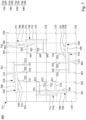
- FIG. 3 is a top view of the first and second antenna bodies 130 and 140 and the defective ground structure layer 111 in the antenna system 100 in FIG. 1 . It should be noted that in order to facilitate the explanation of the positional relationship among the first and second antenna bodies 130 and 140 and the defective ground structure layer 111 , the second insulating plate 121 positioned among the first and second antenna bodies 130 and 140 and the defective ground structure layer 111 is not shown in FIG. 3 .
- the defective ground structure layer 111 includes a plurality of gaps in the first direction and a plurality of gaps in the second direction, and the plurality of gaps in the first direction are perpendicular to the plurality of gaps in the second direction.
- the aforementioned plurality of gaps in the first direction can include a first gap 361 in the first direction, a second gap 362 in the first direction, a third gap 363 in the first direction, a fourth gap 364 in the first direction, a fifth gap 365 in the first direction and a sixth gap 366 in the first direction, in order equally spaced from each other.
- the aforementioned plurality of gaps in the second direction can include a first gap 371 in the second direction, a second gap 372 in the second direction, a third gap 373 in the second direction, a fourth gap 374 in the second direction, a fifth gap 375 in the second direction and sixth gap 376 in the second direction, in order equally spaced from each other.
- the first and second antenna bodies 130 and 140 overlap the aforementioned plurality of gaps in the first and second direction; specifically, the first and second inverted-F antennas 220 and 320 and the first and second asymmetrical T-structure components 210 and 310 overlap the first to the sixth gaps 371 - 376 in the second direction and the first to the sixth gaps 361 - 366 in the first direction.
- the periodic structure is engraved on the defective ground structure layer 111 through the gaps in the first and second directions to perturb the current path, so as to achieve the purpose of reducing the size and increasing or decreasing the modes.
- the first T-shaped extension part 230 of the first inverted-F antenna 220 is positioned between the first gap 361 in the first direction and the second gap 362 in the first direction, the first step impedance transformation part 223 of the first inverted-F antenna 220 is positioned on the second gap 362 in the first direction, the end of the first step impedance transformation part 223 has the first signal feed point 131 , the first connecting part 222 of the first inverted-F antenna 220 is positioned on the third gap 362 in the first direction, the end of the first connecting part 222 part has the first via 132 , the first via 132 is electrically connected to the ground layer 113 (shown in FIG.
- the component 212 of the first asymmetrical T-structure component 210 can be optionally positioned between the third gap 363 in the first direction and the fourth gap 364 in the first direction.
- the second connecting part 322 of the second inverted-F antenna 320 is positioned on the fourth gap 364 in the first direction, the end of the second connecting part 322 has the third via 142 , and the third via 142 is electrically connected to the ground layer 113 (shown in FIG.
- the second main part 321 of the second inverted-F antenna 320 is positioned on the sixth gap 376 in the second direction
- the second T-shaped extension part 330 and the second straight-line extension part 340 are respectively positioned at the opposite sides of the second main part 321 of the second inverted-F antenna 320
- the second asymmetrical T-structure component 310 has the fourth via 143
- the fourth via 143 is electrically connected to the ground layer 113 (shown in FIG.
Landscapes
- Engineering & Computer Science (AREA)
- Computer Networks & Wireless Communication (AREA)
- Waveguide Aerials (AREA)
Abstract
Description
Claims (18)
Applications Claiming Priority (2)
| Application Number | Priority Date | Filing Date | Title |
|---|---|---|---|
| CN202211124155.7A CN117748116A (en) | 2022-09-15 | 2022-09-15 | Antenna system |
| CN202211124155.7 | 2022-09-15 |
Publications (2)
| Publication Number | Publication Date |
|---|---|
| US20240097351A1 US20240097351A1 (en) | 2024-03-21 |
| US12212072B2 true US12212072B2 (en) | 2025-01-28 |
Family
ID=90243241
Family Applications (1)
| Application Number | Title | Priority Date | Filing Date |
|---|---|---|---|
| US18/067,739 Active 2043-05-09 US12212072B2 (en) | 2022-09-15 | 2022-12-19 | Antenna system |
Country Status (2)
| Country | Link |
|---|---|
| US (1) | US12212072B2 (en) |
| CN (1) | CN117748116A (en) |
Citations (4)
| Publication number | Priority date | Publication date | Assignee | Title |
|---|---|---|---|---|
| US8570114B2 (en) * | 2010-09-08 | 2013-10-29 | National Taiwan University | Defected ground structure with shielding effect |
| US20170141465A1 (en) * | 2015-11-12 | 2017-05-18 | King Fahd University Of Petroleum And Minerals | Integrated microwave-millimeter wave antenna system with isolation enhancement mechanism |
| US20190165476A1 (en) * | 2017-11-29 | 2019-05-30 | The Board Of Trustees Of The University Of Alabama | Low-profile multi-band stacked patch antenna |
| US20210210855A1 (en) * | 2020-01-02 | 2021-07-08 | Hughes Network Systems, Llc | Dual-polarized corner-truncated stacked patch antenna with enhanced suppression of cross-polarization and scan performance for wide scan angles |
-
2022
- 2022-09-15 CN CN202211124155.7A patent/CN117748116A/en active Pending
- 2022-12-19 US US18/067,739 patent/US12212072B2/en active Active
Patent Citations (4)
| Publication number | Priority date | Publication date | Assignee | Title |
|---|---|---|---|---|
| US8570114B2 (en) * | 2010-09-08 | 2013-10-29 | National Taiwan University | Defected ground structure with shielding effect |
| US20170141465A1 (en) * | 2015-11-12 | 2017-05-18 | King Fahd University Of Petroleum And Minerals | Integrated microwave-millimeter wave antenna system with isolation enhancement mechanism |
| US20190165476A1 (en) * | 2017-11-29 | 2019-05-30 | The Board Of Trustees Of The University Of Alabama | Low-profile multi-band stacked patch antenna |
| US20210210855A1 (en) * | 2020-01-02 | 2021-07-08 | Hughes Network Systems, Llc | Dual-polarized corner-truncated stacked patch antenna with enhanced suppression of cross-polarization and scan performance for wide scan angles |
Non-Patent Citations (1)
| Title |
|---|
| Da Qing Liu et al., "An Extremely Low-Profile Wideband MIMO Antenna for 5G Smart-phones." IEEE Transactions on Antennas and Propagation, vol. 67, No. 9, 2019, pp. 5772-5780. |
Also Published As
| Publication number | Publication date |
|---|---|
| US20240097351A1 (en) | 2024-03-21 |
| CN117748116A (en) | 2024-03-22 |
Similar Documents
| Publication | Publication Date | Title |
|---|---|---|
| US7330161B2 (en) | Antenna, radio device, method of designing antenna, and method of measuring operating frequency of antenna | |
| US7242353B2 (en) | Bracket-antenna assembly and manufacturing method of the same | |
| US7623087B2 (en) | High-impedance substrate, antenna device and mobile radio device | |
| US6677909B2 (en) | Dual band slot antenna with single feed line | |
| US12191574B2 (en) | Antenna array device | |
| US7800550B2 (en) | Dipole antenna array | |
| US11271326B2 (en) | Antenna system | |
| US12212072B2 (en) | Antenna system | |
| CN111430863A (en) | Transmission line and terminal device | |
| US7898483B2 (en) | Digital TV antenna | |
| KR20050060947A (en) | Stacked microstrip antenna using metal sheet with aperture | |
| US12119566B2 (en) | Communication device | |
| CN114447588B (en) | Antenna structure and electronic device | |
| CN117276898A (en) | Feed system and antenna | |
| US11217887B2 (en) | Antenna module | |
| CN108400436B (en) | Antenna module | |
| TWI822340B (en) | Antenna system | |
| US20250286266A1 (en) | Speaker module, antenna module and electronic device | |
| CN114709602B (en) | Antenna and communication equipment | |
| CN214336910U (en) | Circularly polarized antenna, antenna array and electronic equipment | |
| CN118040315B (en) | Antenna device and electronic equipment | |
| CN219833009U (en) | Antenna unit, antenna array and electronic equipment | |
| US11942699B2 (en) | Antenna device | |
| CN221508486U (en) | MIMO antenna and mobile terminal | |
| CN221126250U (en) | Dual polarized antenna, array antenna and communication device |
Legal Events
| Date | Code | Title | Description |
|---|---|---|---|
| AS | Assignment |
Owner name: INVENTEC CORPORATION, TAIWAN Free format text: ASSIGNMENT OF ASSIGNORS INTEREST;ASSIGNORS:LIN, HSIN HUNG;TAI, YU SHU;CHENG, WEI CHEN;REEL/FRAME:062148/0637 Effective date: 20221215 Owner name: INVENTEC (PUDONG) TECHNOLOGY CORPORATION, CHINA Free format text: ASSIGNMENT OF ASSIGNORS INTEREST;ASSIGNORS:LIN, HSIN HUNG;TAI, YU SHU;CHENG, WEI CHEN;REEL/FRAME:062148/0637 Effective date: 20221215 |
|
| FEPP | Fee payment procedure |
Free format text: ENTITY STATUS SET TO UNDISCOUNTED (ORIGINAL EVENT CODE: BIG.); ENTITY STATUS OF PATENT OWNER: LARGE ENTITY |
|
| STPP | Information on status: patent application and granting procedure in general |
Free format text: DOCKETED NEW CASE - READY FOR EXAMINATION |
|
| STPP | Information on status: patent application and granting procedure in general |
Free format text: NON FINAL ACTION MAILED |
|
| STPP | Information on status: patent application and granting procedure in general |
Free format text: RESPONSE TO NON-FINAL OFFICE ACTION ENTERED AND FORWARDED TO EXAMINER |
|
| STPP | Information on status: patent application and granting procedure in general |
Free format text: NOTICE OF ALLOWANCE MAILED -- APPLICATION RECEIVED IN OFFICE OF PUBLICATIONS |
|
| ZAAB | Notice of allowance mailed |
Free format text: ORIGINAL CODE: MN/=. |
|
| STPP | Information on status: patent application and granting procedure in general |
Free format text: PUBLICATIONS -- ISSUE FEE PAYMENT VERIFIED |
|
| STCF | Information on status: patent grant |
Free format text: PATENTED CASE |