US12211435B2 - Display panel transistor gate-signal compensation systems and methods - Google Patents
Display panel transistor gate-signal compensation systems and methods Download PDFInfo
- Publication number
- US12211435B2 US12211435B2 US18/470,216 US202318470216A US12211435B2 US 12211435 B2 US12211435 B2 US 12211435B2 US 202318470216 A US202318470216 A US 202318470216A US 12211435 B2 US12211435 B2 US 12211435B2
- Authority
- US
- United States
- Prior art keywords
- response
- pixels
- goa
- gate
- signal
- Prior art date
- Legal status (The legal status is an assumption and is not a legal conclusion. Google has not performed a legal analysis and makes no representation as to the accuracy of the status listed.)
- Active
Links
- 238000000034 method Methods 0.000 title claims description 31
- 230000004913 activation Effects 0.000 claims abstract description 81
- 230000004044 response Effects 0.000 claims abstract description 75
- 230000032683 aging Effects 0.000 claims description 44
- 238000012545 processing Methods 0.000 claims description 41
- 230000008859 change Effects 0.000 claims description 11
- 238000004519 manufacturing process Methods 0.000 claims description 8
- 238000005259 measurement Methods 0.000 claims description 8
- 239000010409 thin film Substances 0.000 claims description 3
- 238000001994 activation Methods 0.000 description 54
- 230000008569 process Effects 0.000 description 18
- 230000000630 rising effect Effects 0.000 description 17
- 230000000694 effects Effects 0.000 description 11
- 230000005055 memory storage Effects 0.000 description 8
- 230000003679 aging effect Effects 0.000 description 7
- 230000003111 delayed effect Effects 0.000 description 7
- 230000003287 optical effect Effects 0.000 description 6
- 239000000872 buffer Substances 0.000 description 5
- 238000010586 diagram Methods 0.000 description 4
- 230000007613 environmental effect Effects 0.000 description 3
- 230000006870 function Effects 0.000 description 3
- 239000004973 liquid crystal related substance Substances 0.000 description 3
- 238000012800 visualization Methods 0.000 description 3
- 241000023320 Luma <angiosperm> Species 0.000 description 2
- 230000008901 benefit Effects 0.000 description 2
- 230000005540 biological transmission Effects 0.000 description 2
- 230000001276 controlling effect Effects 0.000 description 2
- 230000003247 decreasing effect Effects 0.000 description 2
- 238000013461 design Methods 0.000 description 2
- 238000011161 development Methods 0.000 description 2
- 230000018109 developmental process Effects 0.000 description 2
- OSWPMRLSEDHDFF-UHFFFAOYSA-N methyl salicylate Chemical compound COC(=O)C1=CC=CC=C1O OSWPMRLSEDHDFF-UHFFFAOYSA-N 0.000 description 2
- 238000012986 modification Methods 0.000 description 2
- 230000004048 modification Effects 0.000 description 2
- 230000009467 reduction Effects 0.000 description 2
- 230000001105 regulatory effect Effects 0.000 description 2
- 230000007704 transition Effects 0.000 description 2
- 102100021935 C-C motif chemokine 26 Human genes 0.000 description 1
- 101100127285 Drosophila melanogaster unc-104 gene Proteins 0.000 description 1
- 101000897493 Homo sapiens C-C motif chemokine 26 Proteins 0.000 description 1
- WHXSMMKQMYFTQS-UHFFFAOYSA-N Lithium Chemical compound [Li] WHXSMMKQMYFTQS-UHFFFAOYSA-N 0.000 description 1
- 241000699666 Mus <mouse, genus> Species 0.000 description 1
- 241000699670 Mus sp. Species 0.000 description 1
- 230000004075 alteration Effects 0.000 description 1
- 238000003491 array Methods 0.000 description 1
- 230000003190 augmentative effect Effects 0.000 description 1
- 230000006399 behavior Effects 0.000 description 1
- 230000001413 cellular effect Effects 0.000 description 1
- 238000004891 communication Methods 0.000 description 1
- 238000004590 computer program Methods 0.000 description 1
- 238000005516 engineering process Methods 0.000 description 1
- 238000007667 floating Methods 0.000 description 1
- 230000002431 foraging effect Effects 0.000 description 1
- 229910052744 lithium Inorganic materials 0.000 description 1
- 230000007774 longterm Effects 0.000 description 1
- 239000000463 material Substances 0.000 description 1
- 230000002093 peripheral effect Effects 0.000 description 1
- 230000010363 phase shift Effects 0.000 description 1
- 229920000642 polymer Polymers 0.000 description 1
- 238000000926 separation method Methods 0.000 description 1
- 238000004904 shortening Methods 0.000 description 1
- 230000035882 stress Effects 0.000 description 1
- 230000000007 visual effect Effects 0.000 description 1
Images


Classifications
-
- G—PHYSICS
- G09—EDUCATION; CRYPTOGRAPHY; DISPLAY; ADVERTISING; SEALS
- G09G—ARRANGEMENTS OR CIRCUITS FOR CONTROL OF INDICATING DEVICES USING STATIC MEANS TO PRESENT VARIABLE INFORMATION
- G09G3/00—Control arrangements or circuits, of interest only in connection with visual indicators other than cathode-ray tubes
- G09G3/20—Control arrangements or circuits, of interest only in connection with visual indicators other than cathode-ray tubes for presentation of an assembly of a number of characters, e.g. a page, by composing the assembly by combination of individual elements arranged in a matrix no fixed position being assigned to or needed to be assigned to the individual characters or partial characters
- G09G3/22—Control arrangements or circuits, of interest only in connection with visual indicators other than cathode-ray tubes for presentation of an assembly of a number of characters, e.g. a page, by composing the assembly by combination of individual elements arranged in a matrix no fixed position being assigned to or needed to be assigned to the individual characters or partial characters using controlled light sources
- G09G3/30—Control arrangements or circuits, of interest only in connection with visual indicators other than cathode-ray tubes for presentation of an assembly of a number of characters, e.g. a page, by composing the assembly by combination of individual elements arranged in a matrix no fixed position being assigned to or needed to be assigned to the individual characters or partial characters using controlled light sources using electroluminescent panels
- G09G3/32—Control arrangements or circuits, of interest only in connection with visual indicators other than cathode-ray tubes for presentation of an assembly of a number of characters, e.g. a page, by composing the assembly by combination of individual elements arranged in a matrix no fixed position being assigned to or needed to be assigned to the individual characters or partial characters using controlled light sources using electroluminescent panels semiconductive, e.g. using light-emitting diodes [LED]
- G09G3/3208—Control arrangements or circuits, of interest only in connection with visual indicators other than cathode-ray tubes for presentation of an assembly of a number of characters, e.g. a page, by composing the assembly by combination of individual elements arranged in a matrix no fixed position being assigned to or needed to be assigned to the individual characters or partial characters using controlled light sources using electroluminescent panels semiconductive, e.g. using light-emitting diodes [LED] organic, e.g. using organic light-emitting diodes [OLED]
- G09G3/3225—Control arrangements or circuits, of interest only in connection with visual indicators other than cathode-ray tubes for presentation of an assembly of a number of characters, e.g. a page, by composing the assembly by combination of individual elements arranged in a matrix no fixed position being assigned to or needed to be assigned to the individual characters or partial characters using controlled light sources using electroluminescent panels semiconductive, e.g. using light-emitting diodes [LED] organic, e.g. using organic light-emitting diodes [OLED] using an active matrix
- G09G3/3233—Control arrangements or circuits, of interest only in connection with visual indicators other than cathode-ray tubes for presentation of an assembly of a number of characters, e.g. a page, by composing the assembly by combination of individual elements arranged in a matrix no fixed position being assigned to or needed to be assigned to the individual characters or partial characters using controlled light sources using electroluminescent panels semiconductive, e.g. using light-emitting diodes [LED] organic, e.g. using organic light-emitting diodes [OLED] using an active matrix with pixel circuitry controlling the current through the light-emitting element
-
- G—PHYSICS
- G09—EDUCATION; CRYPTOGRAPHY; DISPLAY; ADVERTISING; SEALS
- G09G—ARRANGEMENTS OR CIRCUITS FOR CONTROL OF INDICATING DEVICES USING STATIC MEANS TO PRESENT VARIABLE INFORMATION
- G09G3/00—Control arrangements or circuits, of interest only in connection with visual indicators other than cathode-ray tubes
- G09G3/20—Control arrangements or circuits, of interest only in connection with visual indicators other than cathode-ray tubes for presentation of an assembly of a number of characters, e.g. a page, by composing the assembly by combination of individual elements arranged in a matrix no fixed position being assigned to or needed to be assigned to the individual characters or partial characters
- G09G3/22—Control arrangements or circuits, of interest only in connection with visual indicators other than cathode-ray tubes for presentation of an assembly of a number of characters, e.g. a page, by composing the assembly by combination of individual elements arranged in a matrix no fixed position being assigned to or needed to be assigned to the individual characters or partial characters using controlled light sources
- G09G3/30—Control arrangements or circuits, of interest only in connection with visual indicators other than cathode-ray tubes for presentation of an assembly of a number of characters, e.g. a page, by composing the assembly by combination of individual elements arranged in a matrix no fixed position being assigned to or needed to be assigned to the individual characters or partial characters using controlled light sources using electroluminescent panels
- G09G3/32—Control arrangements or circuits, of interest only in connection with visual indicators other than cathode-ray tubes for presentation of an assembly of a number of characters, e.g. a page, by composing the assembly by combination of individual elements arranged in a matrix no fixed position being assigned to or needed to be assigned to the individual characters or partial characters using controlled light sources using electroluminescent panels semiconductive, e.g. using light-emitting diodes [LED]
- G09G3/3208—Control arrangements or circuits, of interest only in connection with visual indicators other than cathode-ray tubes for presentation of an assembly of a number of characters, e.g. a page, by composing the assembly by combination of individual elements arranged in a matrix no fixed position being assigned to or needed to be assigned to the individual characters or partial characters using controlled light sources using electroluminescent panels semiconductive, e.g. using light-emitting diodes [LED] organic, e.g. using organic light-emitting diodes [OLED]
-
- G—PHYSICS
- G09—EDUCATION; CRYPTOGRAPHY; DISPLAY; ADVERTISING; SEALS
- G09G—ARRANGEMENTS OR CIRCUITS FOR CONTROL OF INDICATING DEVICES USING STATIC MEANS TO PRESENT VARIABLE INFORMATION
- G09G2300/00—Aspects of the constitution of display devices
- G09G2300/04—Structural and physical details of display devices
- G09G2300/0404—Matrix technologies
- G09G2300/0408—Integration of the drivers onto the display substrate
-
- G—PHYSICS
- G09—EDUCATION; CRYPTOGRAPHY; DISPLAY; ADVERTISING; SEALS
- G09G—ARRANGEMENTS OR CIRCUITS FOR CONTROL OF INDICATING DEVICES USING STATIC MEANS TO PRESENT VARIABLE INFORMATION
- G09G2300/00—Aspects of the constitution of display devices
- G09G2300/04—Structural and physical details of display devices
- G09G2300/0404—Matrix technologies
- G09G2300/0413—Details of dummy pixels or dummy lines in flat panels
-
- G—PHYSICS
- G09—EDUCATION; CRYPTOGRAPHY; DISPLAY; ADVERTISING; SEALS
- G09G—ARRANGEMENTS OR CIRCUITS FOR CONTROL OF INDICATING DEVICES USING STATIC MEANS TO PRESENT VARIABLE INFORMATION
- G09G2310/00—Command of the display device
- G09G2310/02—Addressing, scanning or driving the display screen or processing steps related thereto
- G09G2310/0264—Details of driving circuits
- G09G2310/0289—Details of voltage level shifters arranged for use in a driving circuit
-
- G—PHYSICS
- G09—EDUCATION; CRYPTOGRAPHY; DISPLAY; ADVERTISING; SEALS
- G09G—ARRANGEMENTS OR CIRCUITS FOR CONTROL OF INDICATING DEVICES USING STATIC MEANS TO PRESENT VARIABLE INFORMATION
- G09G2320/00—Control of display operating conditions
- G09G2320/04—Maintaining the quality of display appearance
- G09G2320/043—Preventing or counteracting the effects of ageing
- G09G2320/045—Compensation of drifts in the characteristics of light emitting or modulating elements
Definitions
- the present disclosure generally relates to sensing gate signals on an electronic display to enable compensation for changes in gate signal behavior over time.
- the display pixels of the display panel may be driven with different current/voltage levels according to the display image data.
- the electronic display includes an array of thin-film transistors (TFTs) (e.g., oxide TFTs), also known as a gate-on-array (GOA), that buffer activation signals to regulate the voltage and/or current supplied to the display pixels.
- TFTs thin-film transistors
- Such driving circuitry may also include a timing controller (TCON) to control activations of the GOA that aids in supplying the data signals (e.g., dataline voltages or currents) to the display pixels.
- TCON timing controller
- the buffered GOA activation signals e.g., gate signals
- the gate signals of the GOA are set such that the “on” time is aligned with the data signals for transmission to the display pixels.
- the rising and falling edges of the GOA outputs are set to be time-aligned with the data signals to provide the desired amount of voltage and/or current to the display pixels.
- the characteristic response of the TFTs e.g., rising and falling edges
- the same GOA input activation signal may change.
- the effective on time (e.g., time between rising and falling edges at a threshold activation level) of an aged TFT may be reduced and/or shifted in time when compared to that of a less aged TFT.
- Such a reduction or shift in the effective on time may result in a different amount of voltage/current than intended being supplied to a display pixel, which may lead to image artifacts such as variations in luminance or color output of the display pixel.
- the effect of aging on the GOA may be measured by sensing the gate signal (e.g., gate signal voltage) output from the GOA and determining a change in the gate signal over the life of electronic device.
- the gate signal may be measured at the output of the GOA for any row of display pixels or for a row of dummy pixels separate from the active area display pixels.
- the current utilization of the display pixels or dummy pixels may be sensed, and changes in the sensed current over the life of the GOA may be indicative of aging.
- the voltage and/or relative phase of the GOA activation signal may be altered based on an estimated amount of aging (e.g., based on the sensed gate signal voltage or pixel current). For example, the voltage levels of the GOA activation signal (e.g., from the level shifter) may be increased (and/or the reference voltage decreased) to adjust the on time of the TFT buffers and counter the effects of GOA aging. Additionally or alternatively, the phase (e.g., timing) of the GOA activation signal relative to the data signals may be altered. For example, the GOA activation signal may be sped up and/or the data signal may be delayed such that a shift in the on time due to aging is countered by the phase change.
- the data signal may be altered (e.g., during image processing) to counter the optical effects (e.g., luminance or color shifts) of the changes in the dataline voltage/current applied to the display pixels.
- FIG. 1 is a schematic block diagram of an electronic device, in accordance with an embodiment:
- FIG. 2 is a front view of a mobile phone representing an example of the electronic device of FIG. 1 , in accordance with an embodiment:
- FIG. 3 is a front view of a tablet device representing an example of the electronic device of FIG. 1 , in accordance with an embodiment:
- FIG. 4 is a front view of a notebook computer representing an example of the electronic device of FIG. 1 , in accordance with an embodiment:
- FIG. 5 is a front and side view of a watch representing an example of the electronic device of FIG. 1 , in accordance with an embodiment
- FIG. 6 is a front view of a computer representing an example of the electronic device of FIG. 1 , in accordance with an embodiment
- FIG. 7 is a block diagram of a portion of the image processing circuitry of FIG. 1 including a gate-on-array (GOA) compensation block, in accordance with an embodiment
- FIG. 8 is a block diagram of a portion of a display panel including an active area of display pixels, a timing controller (TCON), and a GOA, in accordance with an embodiment
- FIG. 9 is a set of graphs of a gate signal and a data signal at multiple ages of the GOA relative to a square waveform, in accordance with an embodiment
- FIG. 10 is the portion of the display panel of FIG. 8 including gate-signal sensing circuitry and gate-signal compensation circuitry, in accordance with an embodiment
- FIG. 11 is the portion of the display panel of FIG. 10 including dummy pixels, in accordance with an embodiment
- FIG. 12 is the portion of the display panel of FIG. 10 including dummy pixels and selector switches, in accordance with an embodiment
- FIG. 13 is the portion of the display panel of FIG. 8 including pixel-current sensing circuitry, gate-signal compensation circuitry, and dummy pixels in a row, in accordance with an embodiment
- FIG. 14 is the portion of the display panel of FIG. 13 with grouped dummy pixels in a dummy row, in accordance with an embodiment:
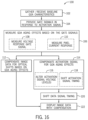
- FIG. 15 is the portion of the display panel of FIG. 8 including pixel-current sensing circuitry, gate-signal compensation circuitry, and dummy pixels in multiple rows, in accordance with an embodiment
- FIG. 16 is a flowchart of an example process for compensating for GOA aging, in accordance with an embodiment.
- the articles “a,” “an,” and “the” are intended to mean that there are one or more of the elements.
- the terms “including” and “having” are intended to be inclusive and mean that there may be additional elements other than the listed elements.
- references to “some embodiments,” “embodiments,” “one embodiment,” or “an embodiment” of the present disclosure are not intended to be interpreted as excluding the existence of additional embodiments that also incorporate the recited features.
- the phrase A “based on” B is intended to mean that A is at least partially based on B.
- the term “or” is intended to be inclusive (e.g., logical OR) and not exclusive (e.g., logical XOR). In other words, the phrase A “or” B is intended to mean A, B, or both A and B.
- Electronic devices often use electronic displays to present visual information. Such electronic devices may include computers, mobile phones, portable media devices, tablets, televisions, virtual-reality headsets, and vehicle dashboards, among many others.
- an electronic display controls the luminance (and, as a consequence, the color) of its display pixels based on corresponding image data received at a particular resolution.
- the display pixels may include self-emissive pixels such as light emitting diodes (LEDs), organic LEDs (OLEDs), etc. or utilize transmissivity regulating elements such as liquid crystal pixels.
- self-emissive pixels generate light indicative of a target luminance level according to the image data associated with the corresponding pixel.
- transmissive displays e.g., liquid crystal displays (LCDs) utilize one or more backlights to generate light and regulate the amount and/or color of the generated light via transmissivity regulating elements according to the image data.
- An image data source may provide the image data as a stream of pixel data, in which data for each pixel indicates a target luminance (e.g., brightness and/or color) of one or more display pixels located at corresponding pixel positions.
- image data may indicate target luminance per color component, for example, via red component image data, blue component image data, and green component image data, collectively referred to as RGB image data (e.g., RGB, SRGB).
- RGB image data e.g., RGB, SRGB
- image data may be indicated by a luma channel and one or more chrominance channels (e.g., YCbCr, YUV, etc.), grayscale, or other color basis.
- a luma channel may encompass linear, non-linear, and/or gamma-corrected luminance values and may be of any suitable bit-depth.
- the image data may be processed to account for one or more physical or digital effects associated with displaying the image data. For example, image data may be compensated for pixel aging (e.g., burn-in compensation), cross-talk between electrodes within the electronic device, transitions from previously displayed image data (e.g., pixel drive compensation), warps, contrast control, and/or other factors that may cause distortions or artifacts perceivable to a viewer. Moreover, the image data may be altered to enhance perceived contrast, sharpness, resolution, etc. After processing, display image data may be sent to a display panel for display.
- pixel aging e.g., burn-in compensation
- cross-talk between electrodes within the electronic device e.g., transitions from previously displayed image data (e.g., pixel drive compensation), warps, contrast control, and/or other factors that
- the display pixels of the display panel may be driven with different current/voltage levels according to the display image data.
- the electronic display includes an array of thin-film transistors (TFTs) (e.g., oxide TFTs) that buffer activation signals to regulate the voltage and/or current supplied to the display pixels.
- TFTs thin-film transistors
- Such driving circuitry may also include a timing controller (TCON) to control activations of the TFTs that aid in supplying the data signals (e.g., dataline voltages or currents) to the display pixels.
- the TCON may utilize a level shifter to provide activation signals to the array of TFTs, also known as a gate-on-array (GOA).
- GOA gate-on-array
- the buffered GOA activation signals e.g., gate signals
- the buffered GOA activation signals are set such that the “on” time is aligned with the data signals for transmission to the display pixels.
- the rising and falling edges of the GOA outputs are set to be time aligned with the data signals to provide the desired amount of voltage and/or current to the display pixels.
- the characteristic response of the TFTs e.g., rising and falling edges
- the same GOA input activation signal may change.
- the effective on time (e.g., time between rising and falling edges at a threshold activation level) of an aged TFT may be reduced and/or shifted in time when compared to that of a less aged TFT.
- Such a reduction or shift in the effective on time may result in a different amount of voltage/current than intended being supplied to a display pixel, which may lead to image artifacts such as variations in luminance or color output of the display pixel.
- operating with tighter timing requirements, such as at higher frequency (e.g., refresh rate) or longer vertical blanking may exacerbate such issues.
- some display pixels, such as OLED display pixels may be more sensitive to changes in the dataline voltage/current and, thus, may be more likely to exhibit image artifacts due to GOA aging.
- the effect of aging on the GOA may be measured by sensing the gate signal (e.g., gate signal voltage) output from the GOA and determining a change in the gate signal over time.
- the gate signal may be measured at the output of the GOA for any row of display pixels or for a row of dummy pixels separate from the active area display pixels.
- the current utilization of the display pixels or dummy pixels may be sensed, and changes in the sensed current over the life of the GOA may be indicative of aging.
- the voltage and/or relative phase of the GOA activation signal may be altered based on an estimated amount of aging (e.g., based on the sensed gate signal voltage or pixel current). For example, the voltage levels of the GOA activation signal (e.g., from the level shifter) may be increased (and/or the reference voltage decreased) to adjust the on time of the TFT buffers and counter the effects of GOA aging. Additionally or alternatively, the phase (e.g., timing) of the GOA activation signal relative to the data signals may be altered. For example, the GOA activation signal may be sped up and/or the data signal may be delayed such that a shift in the on time due to aging is countered by the phase change.
- the data signal may be altered (e.g., during image processing) to counter the optical effects (e.g., luminance or color shifts) of the changes in the dataline voltage/current applied to the display pixels.
- FIG. 1 is an example electronic device 10 with an electronic display 12 having independently controlled color component illuminators (e.g., projectors, backlights, etc.).
- the electronic device 10 may be any suitable electronic device, such as a computer, a mobile phone, a portable media device, a tablet, a television, a virtual-reality headset, a wearable device such as a watch, a vehicle dashboard, or the like.
- FIG. 1 is merely one example of a particular implementation and is intended to illustrate the types of components that may be present in an electronic device 10 .
- the electronic device 10 may include one or more electronic displays 12 , input devices 14 , input/output (I/O) ports 16 , a processor core complex 18 having one or more processors or processor cores, local memory 20 , a main memory storage device 22 , a network interface 24 , a power source 26 , and image processing circuitry 28 .
- the various components described in FIG. 1 may include hardware elements (e.g., circuitry), software elements (e.g., a tangible, non-transitory computer-readable medium storing instructions), or a combination of both hardware and software elements.
- the various components may be combined into fewer components or separated into additional components.
- the local memory 20 and the main memory storage device 22 may be included in a single component.
- the image processing circuitry 28 e.g., a graphics processing unit, a display image processing pipeline, etc.
- the processor core complex 18 may be implemented separately.
- the processor core complex 18 is operably coupled with local memory 20 and the main memory storage device 22 .
- the processor core complex 18 may execute instructions stored in local memory 20 or the main memory storage device 22 to perform operations, such as generating or transmitting image data to display on the electronic display 12 .
- the processor core complex 18 may include one or more general purpose microprocessors, one or more application specific integrated circuits (ASICs), one or more field programmable logic arrays (FPGAs), or any combination thereof.
- the local memory 20 or the main memory storage device 22 may store data to be processed by the processor core complex 18 .
- the local memory 20 and/or the main memory storage device 22 may include one or more tangible, non-transitory, computer-readable media.
- the local memory 20 may include random access memory (RAM) and the main memory storage device 22 may include read-only memory (ROM), rewritable non-volatile memory such as flash memory, hard drives, optical discs, or the like.
- the network interface 24 may communicate data with another electronic device or a network.
- the network interface 24 e.g., a radio frequency system
- the electronic device 10 may communicatively couple to a personal area network (PAN), such as a Bluetooth network, a local area network (LAN), such as an 802.11x Wi-Fi network, or a wide area network (WAN), such as a 4G, Long-Term Evolution (LTE), or 5G cellular network.
- PAN personal area network
- LAN local area network
- WAN wide area network
- 4G Long-Term Evolution
- 5G 5G cellular network
- the power source 26 may provide electrical power to operate the processor core complex 18 and/or other components in the electronic device 10 .
- the power source 26 may include any suitable source of energy, such as a rechargeable lithium polymer (Li-poly) battery and/or an alternating current (AC) power converter.
- the I/O ports 16 may enable the electronic device 10 to interface with various other electronic devices.
- the input devices 14 may enable a user to interact with the electronic device 10 .
- the input devices 14 may include buttons, keyboards, mice, trackpads, and the like.
- the electronic display 12 may include touch sensing components that enable user inputs to the electronic device 10 by detecting occurrence and/or position of an object touching its screen (e.g., surface of the electronic display 12 ).
- the electronic display 12 may display a graphical user interface (GUI) (e.g., of an operating system or computer program), an application interface, text, a still image, and/or video content.
- GUI graphical user interface
- the electronic display 12 may include a display panel with one or more display pixels to facilitate displaying images. Additionally, each display pixel may represent one of the sub-pixels that control the luminance of a color component (e.g., red, green, or blue).
- a display pixel may refer to a collection of sub-pixels (e.g., red, green, and blue subpixels) or may refer to a single sub-pixel.
- the electronic display 12 may display an image by controlling the luminance output (e.g., light emission) of the sub-pixels based on corresponding image data.
- pixel or image data may be generated by an image source, such as the processor core complex 18 , a graphics processing unit (GPU), or an image sensor (e.g., camera).
- image data may be received from another electronic device 10 , for example, via the network interface 24 and/or an I/O port 16 .
- the electronic device 10 may include multiple electronic displays 12 and/or may perform image processing (e.g., via the image processing circuitry 28 ) for one or more external electronic displays 12 , such as connected via the network interface 24 and/or the I/O ports 16 .
- the electronic device 10 may be any suitable electronic device.
- a suitable electronic device 10 specifically a handheld device 10 A, is shown in FIG. 2 .
- the handheld device 10 A may be a portable phone, a media player, a personal data organizer, a handheld game platform, and/or the like.
- the handheld device 10 A may be a smartphone, such as an IPHONE® model available from Apple Inc.
- the handheld device 10 A may include an enclosure 30 (e.g., housing) to, for example, protect interior components from physical damage and/or shield them from electromagnetic interference.
- the enclosure 30 may surround, at least partially, the electronic display 12 .
- the electronic display 12 is displaying a graphical user interface (GUI) 32 having an array of icons 34 .
- GUI graphical user interface
- an application program may launch.
- Input devices 14 may be accessed through openings in the enclosure 30 .
- the input devices 14 may enable a user to interact with the handheld device 10 A.
- the input devices 14 may enable the user to activate or deactivate the handheld device 10 A, navigate a user interface to a home screen, navigate a user interface to a user-configurable application screen, activate a voice-recognition feature, provide volume control, and/or toggle between vibrate and ring modes.
- the I/O ports 16 may also open through the enclosure 30 .
- the electronic device may include one or more cameras 36 to capture pictures or video. In some embodiments, a camera 36 may be used in conjunction with a virtual reality or augmented reality visualization on the electronic display 12 .
- FIG. 3 Another example of a suitable electronic device 10 , specifically a tablet device 10 B, is shown in FIG. 3 .
- the tablet device 10 B may be any IPAD® model available from Apple Inc.
- a further example of a suitable electronic device 10 specifically a computer 10 C, is shown in FIG. 4 .
- the computer 10 C may be any MACBOOK® or IMAC® model available from Apple Inc.
- Another example of a suitable electronic device 10 specifically a watch 10 D, is shown in FIG. 5 .
- the watch 10 D may be any APPLE WATCH® model available from Apple Inc.
- the tablet device 10 B, the computer 10 C, and the watch 10 D each also includes an electronic display 12 , input devices 14 , I/O ports 16 , and an enclosure 30 .
- the electronic display 12 may display a GUI 32 .
- the GUI 32 shows a visualization of a clock.
- an application program may launch, such as to transition the GUI 32 to presenting the icons 34 discussed in FIGS. 2 and 3 .
- a computer 10 E may represent another embodiment of the electronic device 10 of FIG. 1 .
- the computer 10 E may be any suitable computer, such as a desktop computer, a server, or a notebook computer, but may also be a standalone media player or video gaming machine.
- the computer 10 E may be an iMac®, a MacBook®, or other similar device by Apple Inc. of Cupertino, California. It should be noted that the computer 10 E may also represent a personal computer (PC) by another manufacturer.
- a similar enclosure 30 may be provided to protect and enclose internal components of the computer 10 E, such as the electronic display 12 .
- a user of the computer 10 E may interact with the computer 10 E using various peripheral input devices 14 , such as a keyboard 14 A or mouse 14 B, which may connect to the computer 10 E.
- the electronic display 12 may display images based at least in part on image data.
- the image data may be processed, for example, via the image processing circuitry 28 .
- the image processing circuitry 28 may process the image data for display on one or more electronic displays 12 .
- the image processing circuitry 28 may include a display pipeline, memory-to-memory scaler and rotator (MSR) circuitry, warp compensation circuitry, or additional hardware or software means for processing image data.
- the image data may be processed by the image processing circuitry 28 to reduce or eliminate image artifacts, compensate for one or more different software or hardware related effects, and/or format the image data for display on one or more electronic displays 12 .
- the present techniques may be implemented in standalone circuitry, software, and/or firmware, and may be considered a part of, separate from, and/or parallel with a display pipeline or MSR circuitry.
- the image processing circuitry 28 may be implemented in the electronic device 10 , in the electronic display 12 , or a combination thereof.
- the image processing circuitry 28 may be included in the processor core complex 18 , a timing controller (TCON) in the electronic display 12 , or any combination thereof.
- TCON timing controller
- image processing is discussed herein as being performed via a number of image data processing blocks, embodiments may include general purpose and/or dedicated hardware or software components to carry out the techniques discussed herein.
- the electronic device 10 may also include an image data source 38 , a display panel 40 , and/or a controller 42 in communication with the image processing circuitry 28 .
- the display panel 40 of the electronic display 12 may be a reflective technology display, a liquid crystal display (LCD), or any other suitable type of display panel 40 .
- the controller 42 may control operation of the image processing circuitry 28 , the image data source 38 , and/or the display panel 40 .
- the controller 42 may include a controller processor 44 and/or controller memory 46 .
- the controller processor 44 may be included in the processor core complex 18 , the image processing circuitry 28 , a timing controller in the electronic display 12 , a separate processing module, or any combination thereof and execute instructions stored in the controller memory 46 . Additionally, in some embodiments, the controller memory 46 may be included in the local memory 20 , the main memory storage device 22 , a separate tangible, non-transitory, computer-readable medium, or any combination thereof.
- the image processing circuitry 28 may receive source image data 48 corresponding to a desired image to be displayed on the electronic display 12 from the image data source 38 .
- the source image data 48 may indicate target characteristics (e.g., pixel data) corresponding to the desired image using any suitable source format, such as an RGB format, an ⁇ RGB format, a YCbCr format, and/or the like.
- the source image data may be fixed or floating point and be of any suitable bit-depth.
- the source image data 48 may reside in a linear color space, a gamma-corrected color space, or any other suitable color space.
- pixels or pixel data may refer to a grouping of sub-pixels (e.g., individual color component pixels such as red, green, and blue) or the sub-pixels themselves.
- the image processing circuitry 28 may operate to process source image data 48 received from the image data source 38 .
- the image data source 38 may include captured images from cameras 36 , images stored in memory, graphics generated by the processor core complex 18 , or a combination thereof.
- the image processing circuitry 28 may include one or more sets of image data processing blocks 50 (e.g., circuitry, modules, or processing stages) such as a gate-on-array (GOA) compensation block 52 .
- GOA gate-on-array
- multiple other processing blocks 54 may also be incorporated into the image processing circuitry 28 , such as a color management block, a pixel contrast control (PCC) block, a burn-in compensation (BIC) block, a scaling/rotation block, etc.
- PCC pixel contrast control
- BIC burn-in compensation
- the image data processing blocks 50 may receive and process source image data 48 and output display image data 56 in a format (e.g., digital format and/or resolution) interpretable by the display panel 40 . Further, the functions (e.g., operations) performed by the image processing circuitry 28 may be divided between various image data processing blocks 50 , and, while the term “block” is used herein, there may or may not be a logical or physical separation between the image data processing blocks 50 .
- the GOA compensation block 52 may adjust image data (e.g., by color component and/or grey level), for example, to facilitate compensating for GOA aging related effects.
- the image data may be compensated to counter the optical effects (e.g., luminance or color shifts) of the changes in the dataline voltage/current applied to the display pixels due to aging of the GOA.
- the GOA compensation block 52 of the image processing circuitry is one of multiple potential compensations for GOA aging. As such, the GOA compensation block 52 may or may not be implemented, depending on implementation.
- FIG. 8 is a block diagram of a portion of the display panel 40 including an active area of display pixels 58 , a timing controller (TCON) 60 , and a gate-on-array (GOA) 62 .
- the display pixels 58 may be any suitable type of pixel including self-emissive pixels (e.g., LED, micro LED, OLED, etc.) or transmissive pixels (e.g., LCD).
- the TCON 60 may control emission timings and/or refreshes of the electronic display 12 and generally govern operation of the display panel 40 .
- the TCON 60 may include a level shifter controller 64 to control a level shifter 66 that provides an activation signal 68 to the GOA 62 .
- the level shifter 66 may be implemented as part of the TCON 60 and/or integrated with the level shifter controller 64 .
- the GOA 62 is an array of thin-film-transistors (TFTs) such as oxide TFTs that buffer the activation signal 68 for rows of display pixels 58 in the active area.
- the gate signals 70 e.g., buffered activation signals
- the gate signals 70 may be provided (e.g., row-by-row) along with time aligned data signals, indicative of the display image data 56 , such that a combination (e.g., convolution, summation, multiplication or other combination) of a gate signal 70 and data signal are provided to a display pixel 58 .
- the gate signals 70 may be used to modulate the application of data signals to the display pixels 58 such that the display pixels 58 illuminate at the desired color and/or luminance.
- the display pixels 58 are provided gate signals 70 by row such that the activation signal 68 is buffered for a first row, followed by a second row, and so on until the last row of the active area.
- additional circuitry such as a gamma bus generator, may provide the data signals and/or combine the gate signal 70 with the data signals.
- the characteristics of the gate signals 70 may change.
- the rising and falling edges of the gate signal 70 may have altered (e.g., slower) responses as the age of the GOA 62 increases.
- the altered responses of the GOA 62 may result in changes in the dataline voltage/current applied to the display pixels 58 and, therefore, may lead to image artifacts such as errors in color or luminance output.
- FIG. 1 To help illustrate, FIG. 1
- FIG. 9 is a set of graphs of the gate signal 70 and data signal 72 at multiple ages 74 (e.g., T 0 , T 1 , and T 2 ) of the GOA 62 relative to a square waveform 76 .
- the gate signal 70 attempts to approximate the square waveform 76 and has an on period 78 A, 78 B, 78 C (generally 78 ) that coincides with the data signal 72 .
- the on period 78 may shift and/or change in length.
- the on period 78 C at age T 2 may be delayed relative to and/or shorter than the on period 78 B at age T 1 , which may be delayed relative to and/or shorter than the on period 78 A at age T 0 .
- the on period 78 of the gate signal 70 may become more delayed and/or shorter.
- the relative timing of the on period 78 of the gate signal 70 may get out of sync with the data signal 72 , and the asynchronicity may worsen as the age 74 increases.
- the applied voltage/current to the display pixels 58 may be different than desired, leading to image artifacts.
- the gate signal 70 and data signal 72 of FIG. 9 are given as example signals and for example relative timings and, as such, are non-limiting.
- the age 74 may be estimated and compensation may be introduced in either the analog domain (e.g., by compensating the phase or voltage level of the activation signal 68 ) or the digital domain (e.g., by compensating the display image data 56 , such as via the GOA compensation block 52 ).
- the effects of GOA aging are demonstrated in the characteristics of the gate signals 70 and the voltage/current of the display pixels 58 .
- circuitry may be implemented to analyze the gate signals 70 and/or the pixel currents.
- gate-signal sensing circuitry 80 is used to measure the voltage response of one or more gate signals 70 output from the GOA 62 in response to the activation signal 68 , as shown in FIG. 10 .
- the gate-signal sensing circuitry 80 may receive the gate signal 70 output from a row of the GOA 62 and compare the rising and falling voltage characteristics and/or on period 78 to that of a baseline (e.g., set during manufacturing, taken during an initialization phase of the life of the GOA 62 , etc.).
- a baseline e.g., set during manufacturing, taken during an initialization phase of the life of the GOA 62 , etc.
- any row of gate signals 70 may be utilized by the gate-signal sensing circuitry 80 for comparison to the baseline.
- the last row of the GOA 62 may exhibit the largest deviations due to the previous utilizations of the activation signal 68 by the previous rows of the GOA 62 . As such, it may be desirable to obtain gate signal measurements from one of the later rows (e.g., the last row) of the GOA 62 to better sense the effects of GOA aging.
- the gate-signal sensing circuitry 80 may utilize the activation signal 68 as a comparison upon which to obtain a relative difference in the current (e.g., measured) gate signal 70 and that of the baseline. For example, the gate-signal sensing circuitry 80 may measure the timing difference between the rising edge (or falling edge or both) of the activation signal 68 and the rising edge (or falling edge or both) of the gate signal 70 . As shown in FIG. 9 , the rising edge may become more and more delayed as the GOA 62 ages. As such, as the GOA 62 ages, the timing difference between the rising edge of the activation signal 68 and the rising edge of the gate signal 70 may increase.
- the increase in the timing difference between that of the current (e.g., measured) gate signal 70 and the baseline may be indicative of the phase shift (e.g., delay) of the gate signal 70 due to GOA aging.
- the on period 78 may be directly measured, or the rising and falling edges may be measured and the on period 78 calculated as the difference therebetween.
- the rising and falling edges may be measured according to a threshold activation amount, above which the gate signal 70 is considered “on” and below which the gate signal 70 is considered “off.” As such, by sensing the voltage response of the gate signal 70 output from the GOA 62 by itself or relative to the activation signal 68 the effect of GOA aging may be measured.
- the gate-signal sensing circuitry 80 may output an estimated aging parameter 82 .
- the estimated aging parameter 82 may be any suitable signal indicative of the extent of aging that has occurred to the GOA 62 and may be of any suitable form (e.g., analog or digital).
- the estimated aging parameter 82 may be representative of the rising edge delay, the falling edge delay, the on period 78 length, a time delay of the on period 78 , a quantized age, etc.
- the gate-signal compensation may be performed digitally via an image processing block 50 (e.g., the GOA compensation block 52 ) or in the analog domain such as within the TCON 60 .
- the estimated aging parameter 82 may be communicated to the GOA compensation block 52 , and the image data compensated according to the estimated optical error associated with the GOA aging.
- gate-signal compensation circuitry 84 may receive the estimated aging parameter 82 and adjust the activation signal 68 accordingly (e.g., via the level shifter controller 64 and level shifter 66 ).
- the gate-signal sensing circuitry 80 is depicted outside the TCON 60 and the gate-signal compensation circuitry 84 is depicted inside the TCON 60 , either circuitry may be implemented within or independent of the TCON 60 .
- the TCON 60 may utilize any suitable circuitry to modify the activation signal 68 to compensate the gate signal 70 .
- the gate-signal compensation circuitry 84 alters the voltages of the activation signal 68 and/or the timing of the activation signal 68 and/or the data signal 72 .
- the level shifter 66 output may vary between a reference voltage (e.g., in the inactive state) and an activation voltage of the activation signal 68 .
- the gate-signal compensation circuitry 84 may direct (e.g., via the level shifter controller 64 ) the level shifter 66 to increase the activation voltage of the activation signal 68 and/or decrease the reference voltage.
- the response (e.g., rising and falling edges) of the gate signal 70 may be enhanced such that the length of the on period 78 and/or synchronicity of the on period 78 (e.g., relative to the data signal 72 ) is adjusted to or towards that of the baseline.
- the timing of the activation signal 68 and/or the data signal 72 may be adjusted. Indeed, the TCON 60 may speed up (e.g., via the level shifter controller 64 ) the timing (e.g., phase) of the activation signal 68 relative to the data signal 72 and/or delay the timing (e.g., phase) of the data signal 72 such that the on period 78 of the gate signal 70 is aligned (e.g., in phase) with the data signal 72 application transmitted to the display pixels 58 . As such, the gate signal 70 may be compensated for the aging of the GOA 62 .
- the measurement of the gate signal 70 may be performed on any suitable row of the GOA outputs.
- the different pixel utilizations of different image frames may cause fluctuations in the gate signals 70 that could affect the measurement of the estimated aging.
- a dummy row 86 of dummy pixels 88 may be implemented and supplied by a dummy GOA row 89 , as shown in FIG. 11 , such that consistent measurements may be taken (e.g., via the gate-signal sensing circuitry 80 ).
- the voltage measurements of the gate-signal sensing circuitry 80 may be performed while a known set of data signals 72 are applied to the dummy pixels 88 .
- the gate signal 70 may be measured at one or more different positions along the dummy row 86 (e.g., by closing one of a number of switches 90 ), as shown in FIG. 12 .
- the gate-signal compensation circuitry 84 may compensate for the worst-case scenario (e.g., such that the location with the highest gate signal error is compensated) or may compensate based on an average of the gate signals 70 measured at different locations along the dummy row 86 .
- the dummy GOA row 89 may be identical to other rows of the GOA 62 , and the dummy row 86 of dummy pixels 88 may be identical to the other display pixels 58 . Moreover, the dummy pixels 88 may be located within or outside of the active area, but are not utilized to display the display image data 56 .
- the current response 92 of the display pixels 58 may be measured (e.g., by pixel-current sensing circuitry 94 ), as in FIG. 13 .
- GOA aging may affect the current response of the display pixels 58 (e.g., by shortening or delaying the on period 78 ).
- pixel-current sensing circuitry 94 may measure the current response 92 of one or more display pixels 58 (e.g., dummy pixels 88 ) may be measured and compared to a baseline (e.g., set during manufacturing, measured during an initialization phase, etc.). For example, in response to a known data signal 72 , a pixel or group of pixels may be expected to have a particular current response 92 , according to the baseline. However, as the GOA 62 ages, the current response 92 may change (e.g., decrease) in accordance with the delayed and/or shortened on period 78 .
- the difference between the measured current response 92 and the baseline may be indicative of GOA aging.
- the pixel-current sensing circuitry 94 may measure the current response 92 of a single dummy pixel 88 , a conglomerate (e.g., summation of currents) of a group of dummy pixels 88 , or a conglomerate of the dummy row 86 .
- the dummy row 86 may be segregated into different groups 96 A, 96 B (cumulatively 96 ), as shown in FIG. 14 .
- Different groups 96 may undergo different stress conditions (e.g., different data signals 72 ) such that the dummy pixels 88 are aged by different amounts.
- the aging effect of the dummy pixels 88 may be separated, at least in part, from the aging effect of the GOA 62 .
- the pixel-current sensing circuitry 94 may measure the current response for multiple different groups 96 during the same image frame or across multiple different image frames.
- dummy pixels 88 may be implemented on different rows, as in FIG. 15 .
- the gate signals 70 of multiple different rows may be considered, which may yield additional information about the aging of the components of the GOA 62 .
- the current response 92 may be taken from each row individually or the current response 92 may be an average or summation of the dummy pixels 88 of multiple (e.g., all) rows.
- dummy pixels 88 may be implemented in either a dummy row 86 , across multiple rows, or both depending on implementation. For example, space constraints may favor an additional horizontal dummy row 86 as opposed to a vertical column of dummy pixels 88 , or vice versa.
- the pixel-current sensing circuitry 94 may output an estimated aging parameter 82 , which may be the same as or different from that of the gate-signal sensing circuitry 80 .
- the estimated aging parameter 82 output from the pixel-current sensing circuitry 94 may be indicative of a current response 92 .
- the estimated aging parameter 82 may be provided to the GOA compensation block 52 and/or the gate-signal compensation circuitry 84 .
- estimated aging parameters 82 from both the pixel-current sensing circuitry 94 and the gate-signal sensing circuitry 80 may be utilized to compensate the gate signal 70 .
- FIG. 16 is a flowchart 100 of an example process for compensating the gate signal 70 of a GOA 62 for aging.
- baseline GOA characteristics may be received or gathered (process block 102 ).
- the baseline GOA characteristics e.g., baseline gate signal voltages and timings, baseline pixel current responses, etc.
- gate signals 70 may be provided by the GOA 62 in response to activation signals 68 (process block 104 ).
- the GOA aging effects may be measured (process block 106 ).
- the GOA aging effects may be measured by measuring the voltage response of the gate signal 70 (process block 108 ) and/or measuring the pixel current response 92 (process block 110 ).
- measurement of the gate signal 70 e.g., via the gate-signal sensing circuitry 80
- measurement of the pixel current response 92 e.g., via the pixel-current sensing circuitry 94
- compensation implementation may be performed continuously (e.g., each image frame, every other image frame, every tenth image frame, and so on), periodically (e.g., once per day, once per week, once per month, and so on), and/or in response to other stimuli (e.g., a reboot of the electronic device 10 , an error indication, etc.).
- the image data may be compensated to counter for optical shifts (e.g., color and/or luminance errors) that would otherwise appear due to the GOA aging effects (process block 112 ).
- the activation signal 68 may be compensated for the GOA aging effects (process block 114 ).
- the activation signal compensation may include alteration of the activation signal 68 voltage level(s) (process block 116 ) and/or shifting of the activation signal 68 timing (process block 118 ). Additionally or alternatively to the activation signal compensation, the timing of the data signal 72 may be shifted (process block 120 ).
- the activation signal compensation and the data signal timing shift may be utilized individually or in conjunction with one another to achieve synchronization between the gate signal 70 and the data signal 72 .
- the display image data 56 may be displayed (process block 122 ).
- personally identifiable information should follow privacy policies and practices that are generally recognized as meeting or exceeding industry or governmental requirements for maintaining the privacy of users.
- personally identifiable information data should be managed and handled so as to minimize risks of unintentional or unauthorized access or use, and the nature of authorized use should be clearly indicated to users.
Landscapes
- Engineering & Computer Science (AREA)
- Physics & Mathematics (AREA)
- Computer Hardware Design (AREA)
- General Physics & Mathematics (AREA)
- Theoretical Computer Science (AREA)
- Control Of Indicators Other Than Cathode Ray Tubes (AREA)
Abstract
Description
Claims (22)
Priority Applications (1)
| Application Number | Priority Date | Filing Date | Title |
|---|---|---|---|
| US18/470,216 US12211435B2 (en) | 2022-11-18 | 2023-09-19 | Display panel transistor gate-signal compensation systems and methods |
Applications Claiming Priority (2)
| Application Number | Priority Date | Filing Date | Title |
|---|---|---|---|
| US202263426676P | 2022-11-18 | 2022-11-18 | |
| US18/470,216 US12211435B2 (en) | 2022-11-18 | 2023-09-19 | Display panel transistor gate-signal compensation systems and methods |
Publications (2)
| Publication Number | Publication Date |
|---|---|
| US20240169903A1 US20240169903A1 (en) | 2024-05-23 |
| US12211435B2 true US12211435B2 (en) | 2025-01-28 |
Family
ID=91080181
Family Applications (1)
| Application Number | Title | Priority Date | Filing Date |
|---|---|---|---|
| US18/470,216 Active US12211435B2 (en) | 2022-11-18 | 2023-09-19 | Display panel transistor gate-signal compensation systems and methods |
Country Status (1)
| Country | Link |
|---|---|
| US (1) | US12211435B2 (en) |
Citations (15)
| Publication number | Priority date | Publication date | Assignee | Title |
|---|---|---|---|---|
| US7321348B2 (en) | 2000-05-24 | 2008-01-22 | Eastman Kodak Company | OLED display with aging compensation |
| US20110130981A1 (en) * | 2009-11-30 | 2011-06-02 | Ignis Innovation Inc. | System and methods for aging compensation in amoled displays |
| US20130328852A1 (en) | 2012-06-08 | 2013-12-12 | Apple Inc. | Measurement of transistor threshold voltage on a display system substrate using a replica transistor |
| US20170084229A1 (en) | 2014-05-19 | 2017-03-23 | Commonwealth Scientific And Industrial Research Organisation | High resolution oled display operation circuit |
| US9779665B2 (en) | 2015-02-12 | 2017-10-03 | Samsung Display Co., Ltd. | Gate driver for display device and display device including the same |
| US9886891B2 (en) | 2015-01-26 | 2018-02-06 | Samsung Display Co., Ltd. | Sensing driving circuit and display device including the same |
| KR20180062099A (en) | 2016-11-30 | 2018-06-08 | 엘지디스플레이 주식회사 | Display device |
| US10140920B2 (en) | 2015-04-10 | 2018-11-27 | Boe Technology Group Co., Ltd. | Pixel driving circuit, display device and pixel driving method |
| US10410584B2 (en) | 2017-05-08 | 2019-09-10 | Shenzhen China Star Optoelectronics Semiconductor Display Technology Co., Ltd. | Aging compensation system and method for OLED device |
| US10643546B2 (en) | 2017-12-01 | 2020-05-05 | Lg Display Co., Ltd. | Gate driver and display device including the same |
| US11056053B2 (en) | 2018-08-16 | 2021-07-06 | Samsung Display Co., Ltd. | Display device and method of driving the same |
| US11238793B2 (en) | 2017-10-13 | 2022-02-01 | Boe Technology Group Co., Ltd. | Pixel compensation method and system, display device |
| KR102379188B1 (en) | 2015-09-03 | 2022-03-25 | 엘지디스플레이 주식회사 | Display device and driving method of the same |
| KR20230062015A (en) | 2021-10-29 | 2023-05-09 | 한양대학교 산학협력단 | Display panel and controlling method thereof |
| US20230197011A1 (en) | 2021-12-22 | 2023-06-22 | Lg Display Co., Ltd. | Display device and driving circuit |
-
2023
- 2023-09-19 US US18/470,216 patent/US12211435B2/en active Active
Patent Citations (15)
| Publication number | Priority date | Publication date | Assignee | Title |
|---|---|---|---|---|
| US7321348B2 (en) | 2000-05-24 | 2008-01-22 | Eastman Kodak Company | OLED display with aging compensation |
| US20110130981A1 (en) * | 2009-11-30 | 2011-06-02 | Ignis Innovation Inc. | System and methods for aging compensation in amoled displays |
| US20130328852A1 (en) | 2012-06-08 | 2013-12-12 | Apple Inc. | Measurement of transistor threshold voltage on a display system substrate using a replica transistor |
| US20170084229A1 (en) | 2014-05-19 | 2017-03-23 | Commonwealth Scientific And Industrial Research Organisation | High resolution oled display operation circuit |
| US9886891B2 (en) | 2015-01-26 | 2018-02-06 | Samsung Display Co., Ltd. | Sensing driving circuit and display device including the same |
| US9779665B2 (en) | 2015-02-12 | 2017-10-03 | Samsung Display Co., Ltd. | Gate driver for display device and display device including the same |
| US10140920B2 (en) | 2015-04-10 | 2018-11-27 | Boe Technology Group Co., Ltd. | Pixel driving circuit, display device and pixel driving method |
| KR102379188B1 (en) | 2015-09-03 | 2022-03-25 | 엘지디스플레이 주식회사 | Display device and driving method of the same |
| KR20180062099A (en) | 2016-11-30 | 2018-06-08 | 엘지디스플레이 주식회사 | Display device |
| US10410584B2 (en) | 2017-05-08 | 2019-09-10 | Shenzhen China Star Optoelectronics Semiconductor Display Technology Co., Ltd. | Aging compensation system and method for OLED device |
| US11238793B2 (en) | 2017-10-13 | 2022-02-01 | Boe Technology Group Co., Ltd. | Pixel compensation method and system, display device |
| US10643546B2 (en) | 2017-12-01 | 2020-05-05 | Lg Display Co., Ltd. | Gate driver and display device including the same |
| US11056053B2 (en) | 2018-08-16 | 2021-07-06 | Samsung Display Co., Ltd. | Display device and method of driving the same |
| KR20230062015A (en) | 2021-10-29 | 2023-05-09 | 한양대학교 산학협력단 | Display panel and controlling method thereof |
| US20230197011A1 (en) | 2021-12-22 | 2023-06-22 | Lg Display Co., Ltd. | Display device and driving circuit |
Also Published As
| Publication number | Publication date |
|---|---|
| US20240169903A1 (en) | 2024-05-23 |
Similar Documents
| Publication | Publication Date | Title |
|---|---|---|
| US11205363B2 (en) | Electronic display cross-talk compensation systems and methods | |
| US11735147B1 (en) | Foveated display burn-in statistics and burn-in compensation systems and methods | |
| US20190080656A1 (en) | Electronic display color accuracy compensation | |
| US11004391B2 (en) | Image data compensation based on predicted changes in threshold voltage of pixel transistors | |
| US11688363B2 (en) | Reference pixel stressing for burn-in compensation systems and methods | |
| US11776492B1 (en) | Dynamic backlight color shift compensation systems and methods | |
| US20240257710A1 (en) | Foveated display burn-in statistics and burn-in compensation systems and methods | |
| US20240038154A1 (en) | Frame insertion and frame rate sequencing for panel glitch prevention | |
| US11100839B2 (en) | Noise compensation for displays with non-rectangular borders | |
| US12518697B2 (en) | Brightness based pixel driver power reduction systems and methods | |
| US12499806B2 (en) | Multi-least significant bit (LSB) dithering systems and methods | |
| US12211435B2 (en) | Display panel transistor gate-signal compensation systems and methods | |
| US12020648B2 (en) | Routing fanout coupling estimation and compensation | |
| US11227536B2 (en) | Systems and methods for performing in-frame cleaning | |
| US12125436B1 (en) | Pixel drive circuitry burn-in compensation systems and methods | |
| US12154487B2 (en) | Micro-LED burn-in statistics and compensation systems and methods | |
| US12142219B1 (en) | Inverse pixel burn-in compensation systems and methods | |
| US12380835B2 (en) | Electronic display pixel grouping to mitigate motion blur | |
| US12283258B2 (en) | Two-way communication to allow consistent per-frame configuration update | |
| US20230368718A1 (en) | Display Pixel Non-Uniformity Compensation | |
| US20250037648A1 (en) | Systems and Methods for Providing Fine-Grained Arbitrary Presentation Time for Electronic Displays | |
| US12205510B2 (en) | Spatiotemporal dither for pulsed digital display systems and methods | |
| US20260065824A1 (en) | Display Strain Aware Frame Insertion Frame Rate Sequencing | |
| US12340736B2 (en) | Systems and methods for IR-independent pre-charge and inverter- based IR reduction | |
| US20250157378A1 (en) | Sub-Pixel Uniformity Correction Clip Compensation Systems and Methods |
Legal Events
| Date | Code | Title | Description |
|---|---|---|---|
| AS | Assignment |
Owner name: APPLE INC., CALIFORNIA Free format text: ASSIGNMENT OF ASSIGNORS INTEREST;ASSIGNORS:XIONG, WEI;CHANG, SUN-IL;NHO, HYUNWOO;AND OTHERS;SIGNING DATES FROM 20230815 TO 20230828;REEL/FRAME:064958/0827 |
|
| FEPP | Fee payment procedure |
Free format text: ENTITY STATUS SET TO UNDISCOUNTED (ORIGINAL EVENT CODE: BIG.); ENTITY STATUS OF PATENT OWNER: LARGE ENTITY |
|
| STPP | Information on status: patent application and granting procedure in general |
Free format text: DOCKETED NEW CASE - READY FOR EXAMINATION |
|
| STPP | Information on status: patent application and granting procedure in general |
Free format text: NON FINAL ACTION MAILED |
|
| STPP | Information on status: patent application and granting procedure in general |
Free format text: RESPONSE TO NON-FINAL OFFICE ACTION ENTERED AND FORWARDED TO EXAMINER |
|
| STPP | Information on status: patent application and granting procedure in general |
Free format text: NOTICE OF ALLOWANCE MAILED -- APPLICATION RECEIVED IN OFFICE OF PUBLICATIONS |
|
| STPP | Information on status: patent application and granting procedure in general |
Free format text: PUBLICATIONS -- ISSUE FEE PAYMENT RECEIVED |
|
| STPP | Information on status: patent application and granting procedure in general |
Free format text: PUBLICATIONS -- ISSUE FEE PAYMENT VERIFIED |
|
| STCF | Information on status: patent grant |
Free format text: PATENTED CASE |