US12207548B2 - Light-emitting device and apparatus including the same - Google Patents
Light-emitting device and apparatus including the same Download PDFInfo
- Publication number
- US12207548B2 US12207548B2 US17/030,031 US202017030031A US12207548B2 US 12207548 B2 US12207548 B2 US 12207548B2 US 202017030031 A US202017030031 A US 202017030031A US 12207548 B2 US12207548 B2 US 12207548B2
- Authority
- US
- United States
- Prior art keywords
- group
- substituted
- unsubstituted
- metal
- electrode
- Prior art date
- Legal status (The legal status is an assumption and is not a legal conclusion. Google has not performed a legal analysis and makes no representation as to the accuracy of the status listed.)
- Active, expires
Links
Images


Classifications
-
- H—ELECTRICITY
- H10—SEMICONDUCTOR DEVICES; ELECTRIC SOLID-STATE DEVICES NOT OTHERWISE PROVIDED FOR
- H10K—ORGANIC ELECTRIC SOLID-STATE DEVICES
- H10K71/00—Manufacture or treatment specially adapted for the organic devices covered by this subclass
- H10K71/10—Deposition of organic active material
- H10K71/12—Deposition of organic active material using liquid deposition, e.g. spin coating
-
- C—CHEMISTRY; METALLURGY
- C01—INORGANIC CHEMISTRY
- C01G—COMPOUNDS CONTAINING METALS NOT COVERED BY SUBCLASSES C01D OR C01F
- C01G9/00—Compounds of zinc
- C01G9/02—Oxides; Hydroxides
-
- C—CHEMISTRY; METALLURGY
- C09—DYES; PAINTS; POLISHES; NATURAL RESINS; ADHESIVES; COMPOSITIONS NOT OTHERWISE PROVIDED FOR; APPLICATIONS OF MATERIALS NOT OTHERWISE PROVIDED FOR
- C09K—MATERIALS FOR MISCELLANEOUS APPLICATIONS, NOT PROVIDED FOR ELSEWHERE
- C09K11/00—Luminescent materials, e.g. electroluminescent or chemiluminescent
- C09K11/08—Luminescent materials, e.g. electroluminescent or chemiluminescent containing inorganic luminescent materials
- C09K11/88—Luminescent materials, e.g. electroluminescent or chemiluminescent containing inorganic luminescent materials containing selenium, tellurium or unspecified chalcogen elements
- C09K11/881—Chalcogenides
- C09K11/885—Chalcogenides with alkaline earth metals
-
- H—ELECTRICITY
- H10—SEMICONDUCTOR DEVICES; ELECTRIC SOLID-STATE DEVICES NOT OTHERWISE PROVIDED FOR
- H10K—ORGANIC ELECTRIC SOLID-STATE DEVICES
- H10K50/00—Organic light-emitting devices
- H10K50/10—OLEDs or polymer light-emitting diodes [PLED]
- H10K50/11—OLEDs or polymer light-emitting diodes [PLED] characterised by the electroluminescent [EL] layers
- H10K50/115—OLEDs or polymer light-emitting diodes [PLED] characterised by the electroluminescent [EL] layers comprising active inorganic nanostructures, e.g. luminescent quantum dots
-
- H—ELECTRICITY
- H10—SEMICONDUCTOR DEVICES; ELECTRIC SOLID-STATE DEVICES NOT OTHERWISE PROVIDED FOR
- H10K—ORGANIC ELECTRIC SOLID-STATE DEVICES
- H10K50/00—Organic light-emitting devices
- H10K50/10—OLEDs or polymer light-emitting diodes [PLED]
- H10K50/14—Carrier transporting layers
- H10K50/16—Electron transporting layers
- H10K50/165—Electron transporting layers comprising dopants
-
- H—ELECTRICITY
- H10—SEMICONDUCTOR DEVICES; ELECTRIC SOLID-STATE DEVICES NOT OTHERWISE PROVIDED FOR
- H10K—ORGANIC ELECTRIC SOLID-STATE DEVICES
- H10K50/00—Organic light-emitting devices
- H10K50/10—OLEDs or polymer light-emitting diodes [PLED]
- H10K50/17—Carrier injection layers
- H10K50/171—Electron injection layers
-
- H—ELECTRICITY
- H10—SEMICONDUCTOR DEVICES; ELECTRIC SOLID-STATE DEVICES NOT OTHERWISE PROVIDED FOR
- H10K—ORGANIC ELECTRIC SOLID-STATE DEVICES
- H10K59/00—Integrated devices, or assemblies of multiple devices, comprising at least one organic light-emitting element covered by group H10K50/00
- H10K59/80—Constructional details
- H10K59/805—Electrodes
- H10K59/8052—Cathodes
- H10K59/80524—Transparent cathodes, e.g. comprising thin metal layers
-
- H—ELECTRICITY
- H10—SEMICONDUCTOR DEVICES; ELECTRIC SOLID-STATE DEVICES NOT OTHERWISE PROVIDED FOR
- H10K—ORGANIC ELECTRIC SOLID-STATE DEVICES
- H10K85/00—Organic materials used in the body or electrodes of devices covered by this subclass
- H10K85/30—Coordination compounds
-
- H—ELECTRICITY
- H10—SEMICONDUCTOR DEVICES; ELECTRIC SOLID-STATE DEVICES NOT OTHERWISE PROVIDED FOR
- H10K—ORGANIC ELECTRIC SOLID-STATE DEVICES
- H10K85/00—Organic materials used in the body or electrodes of devices covered by this subclass
- H10K85/50—Organic perovskites; Hybrid organic-inorganic perovskites [HOIP], e.g. CH3NH3PbI3
-
- H—ELECTRICITY
- H10—SEMICONDUCTOR DEVICES; ELECTRIC SOLID-STATE DEVICES NOT OTHERWISE PROVIDED FOR
- H10K—ORGANIC ELECTRIC SOLID-STATE DEVICES
- H10K85/00—Organic materials used in the body or electrodes of devices covered by this subclass
- H10K85/60—Organic compounds having low molecular weight
- H10K85/631—Amine compounds having at least two aryl rest on at least one amine-nitrogen atom, e.g. triphenylamine
-
- H—ELECTRICITY
- H10—SEMICONDUCTOR DEVICES; ELECTRIC SOLID-STATE DEVICES NOT OTHERWISE PROVIDED FOR
- H10K—ORGANIC ELECTRIC SOLID-STATE DEVICES
- H10K85/00—Organic materials used in the body or electrodes of devices covered by this subclass
- H10K85/60—Organic compounds having low molecular weight
- H10K85/649—Aromatic compounds comprising a hetero atom
- H10K85/656—Aromatic compounds comprising a hetero atom comprising two or more different heteroatoms per ring
-
- H—ELECTRICITY
- H10—SEMICONDUCTOR DEVICES; ELECTRIC SOLID-STATE DEVICES NOT OTHERWISE PROVIDED FOR
- H10K—ORGANIC ELECTRIC SOLID-STATE DEVICES
- H10K85/00—Organic materials used in the body or electrodes of devices covered by this subclass
- H10K85/60—Organic compounds having low molecular weight
- H10K85/649—Aromatic compounds comprising a hetero atom
- H10K85/657—Polycyclic condensed heteroaromatic hydrocarbons
- H10K85/6572—Polycyclic condensed heteroaromatic hydrocarbons comprising only nitrogen in the heteroaromatic polycondensed ring system, e.g. phenanthroline or carbazole
-
- B—PERFORMING OPERATIONS; TRANSPORTING
- B82—NANOTECHNOLOGY
- B82Y—SPECIFIC USES OR APPLICATIONS OF NANOSTRUCTURES; MEASUREMENT OR ANALYSIS OF NANOSTRUCTURES; MANUFACTURE OR TREATMENT OF NANOSTRUCTURES
- B82Y20/00—Nanooptics, e.g. quantum optics or photonic crystals
-
- B—PERFORMING OPERATIONS; TRANSPORTING
- B82—NANOTECHNOLOGY
- B82Y—SPECIFIC USES OR APPLICATIONS OF NANOSTRUCTURES; MEASUREMENT OR ANALYSIS OF NANOSTRUCTURES; MANUFACTURE OR TREATMENT OF NANOSTRUCTURES
- B82Y40/00—Manufacture or treatment of nanostructures
-
- H—ELECTRICITY
- H10—SEMICONDUCTOR DEVICES; ELECTRIC SOLID-STATE DEVICES NOT OTHERWISE PROVIDED FOR
- H10K—ORGANIC ELECTRIC SOLID-STATE DEVICES
- H10K50/00—Organic light-emitting devices
- H10K50/10—OLEDs or polymer light-emitting diodes [PLED]
- H10K50/14—Carrier transporting layers
- H10K50/16—Electron transporting layers
-
- Y—GENERAL TAGGING OF NEW TECHNOLOGICAL DEVELOPMENTS; GENERAL TAGGING OF CROSS-SECTIONAL TECHNOLOGIES SPANNING OVER SEVERAL SECTIONS OF THE IPC; TECHNICAL SUBJECTS COVERED BY FORMER USPC CROSS-REFERENCE ART COLLECTIONS [XRACs] AND DIGESTS
- Y10—TECHNICAL SUBJECTS COVERED BY FORMER USPC
- Y10S—TECHNICAL SUBJECTS COVERED BY FORMER USPC CROSS-REFERENCE ART COLLECTIONS [XRACs] AND DIGESTS
- Y10S977/00—Nanotechnology
- Y10S977/70—Nanostructure
- Y10S977/773—Nanoparticle, i.e. structure having three dimensions of 100 nm or less
- Y10S977/774—Exhibiting three-dimensional carrier confinement, e.g. quantum dots
Definitions
- One or more aspects of embodiments of the present disclosure relate to a light-emitting device and an apparatus including the same.
- Light-emitting devices convert electrical into light energy.
- Example light-emitting devices include organic light-emitting devices in which a light-emitting material is an organic material, and quantum dot light-emitting devices in which the light-emitting material is a quantum dot.
- a light-emitting device may have a structure in which a first electrode, a hole transport region, an emission layer, an electron transport region, and a second electrode are sequentially formed. Holes provided from the first electrode may move toward the emission layer through the hole transport region, and electrons provided from the second electrode may move toward the emission layer through the electron transport region. The holes and the electrons may recombine in the emission layer to produce excitons. These excitons may transition from an excited state to the ground state to thereby generate light.
- One or more aspects of embodiments of the present disclosure are directed toward a light-emitting device having excellent emission efficiency and/or lifespan properties, and an apparatus including the same.
- One or more example embodiments of the present disclosure provide an apparatus including the organic light-emitting device.
- the expression “at least one of a, b or c” may indicate only a, only b, only c, both a and b, both a and c, both b and c, all of a, b, and c, or variations thereof.
- room temperature refers to about 25° C.
- the light-emitting device 10 illustrated in the drawing includes a first electrode 110 , an emission layer 153 , an electron transport layer 155 , a metal-nucleation inducing layer 157 , and a second electrode 190 .
- a substrate may be additionally disposed under the first electrode 110 and/or above the second electrode 190 .
- the substrate may be a glass substrate and/or a plastic substrate.
- the first electrode 110 may be formed by depositing or sputtering a material for forming the first electrode 110 on the substrate.
- a high work function material that can easily inject holes may be used as a material for the first electrode 110 .
- the first electrode 110 may be a reflective electrode, a semi-transmissive electrode, or a transparent electrode.
- a material for forming a first electrode may include indium tin oxide (ITO), indium zinc oxide (IZO), tin oxide (SnO 2 ), zinc oxide (ZnO), or any combination thereof.
- ITO indium tin oxide
- IZO indium zinc oxide
- SnO 2 tin oxide
- ZnO zinc oxide
- magnesium (Mg) silver
- silver (Ag) aluminum
- Al—Li aluminum-lithium
- Ca calcium
- magnesium-silver (Mg—Ag) magnesium-silver
- the first electrode 110 may have a single-layered structure including (e.g., consisting of) a single layer, or a multi-layered structure including a plurality of layers.
- the first electrode 110 may have a three-layered structure of ITO/Ag/ITO.
- a hole transport region may be additionally located between the first electrode 110 and the emission layer 153 .
- the hole transport region may have: i) a single-layered structure with a single layer including a single material, ii) a single-layered structure with a single layer including a plurality of different materials, or iii) a multi-layered structure having a plurality of layers including a plurality of different materials.
- the hole transport region may include at least one layer selected from a hole injection layer, a hole transport layer, an emission auxiliary layer, and an electron blocking layer.
- the hole transport region may have a single-layered structure with a single layer including a plurality of different materials, or a multi-layered structure with a hole injection layer/hole transport layer structure, a hole injection layer/hole transport layer/emission auxiliary layer structure, a hole injection layer/emission auxiliary layer structure, a hole transport layer/emission auxiliary layer structure, or a hole injection layer/hole transport layer/electron blocking layer structure, wherein the constituting layers of each structure are sequentially stacked from the first electrode 110 in each stated order.
- the hole transport region may include m-MTDATA, TDATA, 2-TNATA, NPB (NPD), ⁇ -NPB, TPD, Spiro-TPD, spiro-NPB, methylated-NPB, TAPC, HMTPD, 4,4′,4′′-tris(N-carbazolyl)triphenylamine (TCTA), polyaniline/dodecylbenzene sulfonic acid (PANI/DBSA), poly(3,4-ethylene dioxythiophene)/poly(4-styrene sulfonate) (PEDOT:PSS), polyaniline/camphor sulfonic acid (PANI/CSA), polyaniline/poly(4-styrene sulfonate) (PANI/PSS), poly(9,9-dioctyl-fluorene-co-N-(4-butylphenyl)-diphenylamine (TFB), a compound represented by Formula 201,
- R 201 and R 202 may optionally be linked to each other via a single bond, a dimethyl-methylene group, or a diphenyl-methylene group
- R 203 and R 204 may optionally be linked to each other via a single bond, a dimethyl-methylene group, or a diphenyl-methylene group.
- R 201 and R 202 may be linked to each other via a single bond, and/or ii) R 203 and R 204 may be linked to each other via a single bond.
- At least one of R 201 to R 204 in Formula 202 may be a carbazolyl group that is unsubstituted, or substituted with deuterium, —F, —Cl, —Br, —I, a hydroxyl group, a cyano group, a nitro group, an amidino group, a hydrazine group, a hydrazone group, a C 1 -C 20 alkyl group, a C 1 -C 20 alkoxy group, a cyclopentyl group, a cyclohexyl group, a cycloheptyl group, a cyclopentenyl group, a cyclohexenyl group, a phenyl group, a biphenyl group, a terphenyl group, a phenyl group substituted with a C 1 -C 10 alkyl group, a phenyl group substituted with —F, a naph
- the compound represented by Formula 201 may be represented by Formula 201-1:
- the compound represented by Formula 201 may be represented by Formula 201-2:
- the compound represented by Formula 201 may be represented by Formula 201-2(1):
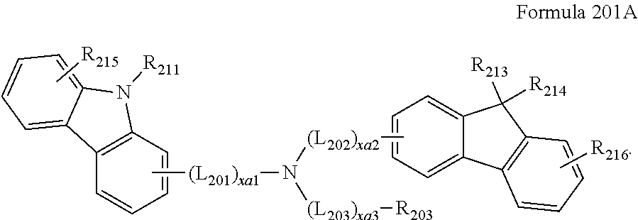
- the compound represented by Formula 201 may be represented by Formula 201A:
- the compound represented by Formula 201 may be represented by Formula 201A(1):
- the compound represented by Formula 201 may be represented by Formula 201A-1:
- the compound represented by Formula 202 may be represented by Formula 202-1:
- the compound represented by Formula 202 may be represented by Formula 202-1(1):
- the compound represented by Formula 202 may be represented by Formula 202A:
- the compound represented by Formula 202 may be represented by Formula 202A-1:
- the hole transport region may include at least one compound selected from Compounds HT1 to HT48:
- a thickness of the hole transport region may be about 100 ⁇ to about 10,000 ⁇ , for example, about 100 ⁇ to about 1,000 ⁇ .
- the thickness of the hole injection layer may be about 100 ⁇ to about 9,000 ⁇ , for example, about 100 ⁇ to about 1,000 ⁇ , and the thickness of the hole transport layer may be about 50 ⁇ to about 2,000 ⁇ , for example, about 100 ⁇ to about 1,500 ⁇ .
- the thicknesses of the hole transport region, the hole injection layer and the hole transport layer are within these ranges, satisfactory hole transporting characteristics may be obtained without a substantial increase in driving voltage.
- the emission auxiliary layer may increase light-emission efficiency by compensating for an optical resonance distance of the wavelength of light emitted by the emission layer 153 , and the electron blocking layer may block or reduce the flow of electrons from the electron transport layer 155 .
- the emission auxiliary layer and the electron blocking layer may each independently include the materials as described above.
- the hole transport region may further include, in addition to these materials, a charge-generation material for the improvement of conductive properties.
- the charge-generation material may be substantially homogeneously or non-homogeneously dispersed in the hole transport region.
- the charge-generation material may be, for example, a p-dopant.
- a lowest unoccupied molecular orbital (LUMO) energy level of the p-dopant may be ⁇ 3.5 eV or less.
- the p-dopant may include a quinone derivative, metal oxide, a cyano group-containing compound, or any combination thereof.
- the p-dopant may include at least one selected from:
- the emission layer 153 may include any organic light-emitting material.
- the organic light-emitting material may include a host and/or a dopant.
- an amount of the dopant may be about 0.01 parts by weight to about 15 parts by weight based on 100 parts by weight of the host.
- a thickness of the emission layer 153 including an organic light-emitting material may be about 100 ⁇ to about 1,000 ⁇ , for example, about 200 ⁇ to about 600 ⁇ . When the thickness of the emission layer 153 is within these ranges, excellent light-emission characteristics may be obtained without a substantial increase in driving voltage.
- the emission layer 153 may include a quantum dot.
- the thickness of the emission layer 153 including the quantum dot may be about 7 nm to about 100 nm, for example, about 15 nm to about 50 nm. Within these ranges, the light-emitting device may have excellent emission efficiency and/or lifespan properties due to the control of pores that may be generated by quantum dot particle arrangement.
- the emission layer 153 may include a plurality of emission layers to emit light of different colors for each sub-pixel.
- the host may include a compound represented by Formula 301: [Ar 301 ] xb11 ⁇ [(L 301 ) xb1 ⁇ R 301 ] xb21 .
- Formula 301 [Ar 301 ] xb11 ⁇ [(L 301 ) xb1 ⁇ R 301 ] xb21 .
- xb11 in Formula 301 when xb11 in Formula 301 is 2 or more, two or more Ar 301 (s) may be linked to each other via a single bond.
- the host may include a compound represented by Formula 301-1, a compound represented by Formula 301-2, or any combination thereof:
- the host may include an alkaline earth metal complex.
- the host may be a Be complex (for example, Compound H55) or a Mg complex.
- the host may be or include a Zn complex, or any combination of the above.
- the phosphorescent dopant may include at least one transition metal as a central metal.
- the phosphorescent dopant may include a monodentate ligand, a bidentate ligand, a tridentate ligand, a tetradentate ligand, a pentadentate ligand, a hexadentate ligand, or any combination thereof.
- the phosphorescent dopant may be electrically neutral.
- the phosphorescent dopant may further include an organometallic compound represented by Formula 401:
- X 401 may be nitrogen
- X 402 may be carbon
- X 401 and X 402 may be nitrogen at the same time.
- two ring A 401 (s) in two or more L 401 (s) may optionally be linked to each other via T 402 , which is a linking group, or two ring A 402 (s) in two or more L 401 (s) may optionally be linked to each other via T 403 , which is a linking group.
- T 402 and T 403 may each independently be the same as described in connection with T 401 .
- L 402 in Formula 401 may be an organic ligand.
- L 402 may be a halogen group, a diketone group (for example, an acetylacetonate group), a carboxylic acid group (for example, picolinate group), —C( ⁇ O), an isonitrile group, a —CN group, a phosphorus group (for example, a phosphine group or a phosphite group), or any combination thereof.
- the fluorescent dopant may include an amine group-containing compound, a styryl group-containing compound, or any combination thereof.
- the fluorescent dopant may include a compound represented by Formula 501:
- Ar 501 in Formula 501 may be a condensed cyclic ring (for example, an anthracene group, a chrysene group, a pyrene group, etc.) in which three or more monocyclic groups are condensed.
- a condensed cyclic ring for example, an anthracene group, a chrysene group, a pyrene group, etc.
- xd4 in Formula 501 may be 2.
- the fluorescent dopant may include an amine group-containing compound, a styryl group-containing compound, or any combination thereof.
- the emission layer 153 may include a quantum dot (dots).
- the emission layer 153 may further include a matrix material in addition to the quantum dots.
- the emission layer 153 may include a quantum dot (dots) and a matrix material, and the quantum dots may be dispersed in the matrix material.
- the quantum dot may include a Group II-VI semiconductor compound; a Group III-VI semiconductor compound; a Group III-V semiconductor compound; a Group IV-VI semiconductor compound; a Group IV element or compound; a Group I-III-VI semiconductor compound; or any combination thereof.
- the Group II-VI semiconductor compound may include a binary compound (such as CdS, CdSe, CdTe, ZnS, ZnSe, ZnTe, ZnO, HgS, HgSe, HgTe, MgS, MgSe, and/or the like); a ternary compound (such as CdSeS, CdSeTe, CdSTe, ZnSeS, ZnSeTe, ZnSTe, HgSeS, HgSeTe, HgSTe, CdZnS, CdZnSe, CdZnTe, CdHgS, CdHgSe, CdHgTe, HgZnS, HgZnSe, HgZnTe, MgZnS, MgZnSe, and/or the like); a quaternary compound (such as CdZnSeS, CdZnSeTe, CdZnSTe, C
- the Group III-VI semiconductor compound may include: a binary compound (such as In 2 S 3 and/or In 2 Se); a ternary compound (such as InGaS 3 and/or InGaSe 3 ); or any combination thereof.
- the Group III-V semiconductor compound may include a binary compound (such as GaN, GaP, GaAs, GaSb, AlN, AlP, AlAs, AlSb, InN, InP, InAs, InSb, and/or the like); a ternary compound (such as GaNP, GaNAs, GaNSb, GaPAs, GaPSb, AlNP, AlNAs, AlNSb, AlPAs, AlPSb, InGaP, InAlP, InNP, InNAs, InNSb, InPAs, InPSb, GaAlNP, and/or the like); a quaternary compound (such as GaAlNAs, GaAlNSb, GaAlPAs, GaAlPSb, GaInNP, GaInNAs, GaInNSb, GaInPAs, GaInPSb, InAlNP, InAlNAs, InAlNSb, InAlPAs, InAlPSb, and/or the like); or any combination thereof.
- the Group IV-VI semiconductor compound may include a binary compound (such as SnS, SnSe, SnTe, PbS, PbSe, PbTe, and/or the like); a ternary compound (such as SnSeS, SnSeTe, SnSTe, PbSeS, PbSeTe, PbSTe, SnPbS, SnPbSe, SnPbTe, and/or the like); a quaternary compound (such as SnPbSSe, SnPbSeTe, SnPbSTe, and/or the like); or any combination thereof.
- a binary compound such as SnS, SnSe, SnTe, PbS, PbSe, PbTe, and/or the like
- a ternary compound such as SnSeS, SnSeTe, SnSTe, PbSTe, and/or the like
- a quaternary compound such
- the Group IV element or a compound including the same may include Si and/or Ge; a binary compound (such as SiC, SiGe, and/or the like); or any combination thereof.
- the Group I-III-VI semiconductor compound may include a ternary compound (such as AgInS, AgInS 2 , CuInS, CuInS 2 , CuGaO 2 , AgGaO 2 , AgAlO 2 , or any combination thereof).
- a ternary compound such as AgInS, AgInS 2 , CuInS, CuInS 2 , CuGaO 2 , AgGaO 2 , AgAlO 2 , or any combination thereof).
- the quantum dot may have a substantially homogeneous structure in terms of components and composition; or a composite structure (such as a core-shell structure, a gradient structure, and/or the like).
- the shell of the core-shell structure may be a single shell having a homogeneous component and composition, or may be a multi-shell structure including two or more layers having different components and/or compositions.
- a material constituting the core and a material constituting the shell may each independently be selected from the semiconductor compounds described above.
- the quantum dot may include a Group III-V semiconductor compound.
- the quantum dot may include In.
- the quantum dot may include In and P.
- the quantum dot may include a Group III-V semiconductor compound and a Group II-VI semiconductor compound.
- the quantum dot may have a core-shell structure, the core may be a Group III-V semiconductor compound, and the shell may be a Group II-VI semiconductor compound.
- the quantum dot may have a core-shell structure
- the core may be GaN, GaP, GaAs, GaSb, AlN, AlP, AlAs, AlSb, InN, InP, InAs, InSb, GaNP, GaNAs, GaNSb, GaPAs, GaPSb, AlNP, AlNAs, AlNSb, AlPAs, AlPSb, InGaP, InAlP, InNP, InNAs, InNSb, InPAs, InPSb, GaAlNP GaAlNAs, GaAlNSb, GaAlPAs, GaAlPSb, GaInNP, GaInNAs, GaInNSb, GaInPAs, GaInPSb, InAlNP, InAlNAs, InAlNSb, InAlPAs, InAlPSb, or any combination thereof
- the shell may be CdS, CdSe, CdTe, ZnS, ZnSe, ZnTe, ZnO
- the quantum dot may have a core-shell structure
- the core may be CdSe, CdS, ZnS, ZnSe, CdTe, CdSeTe, CdZnS, PbSe, AgInZnS, ZnO, InN, InP, InAs, InSb, InGaP or any combination thereof
- the shell may be CdSe, ZnSe, ZnS, ZnSeS ZnTe, CdTe, PbS, TiO, SrSe, HgSe, or any combination thereof.
- the quantum dot may be a InP/ZnS or InP/ZnSeS core-shell quantum dot.
- the quantum dot may be synthesized using any suitable method (such as a wet chemical process, a metal organic chemical vapor deposition process (MOCVD), and/or a molecular beam epitaxy (MBE) process).
- a wet chemical process such as a wet chemical process, a metal organic chemical vapor deposition process (MOCVD), and/or a molecular beam epitaxy (MBE) process.
- MOCVD metal organic chemical vapor deposition process
- MBE molecular beam epitaxy
- An average particle diameter of the quantum dot may be about 1 nm to about 20 nm, for example, about 1 nm to about 15 nm, for example, about 1 nm to about 10 nm.
- the ratio of the radius of the core to the thickness of the shell may be 2:8 to 8:2, for example, 3:7 to 7:3, for example, 4:6 to 6:4.
- the matrix material may include a polymer acting as a medium through which the quantum dots are dispersed.
- Electron Transport Layer 155
- the electron transport layer 155 may be located between the emission layer 153 and the second electrode 190 .
- the electron transport layer 155 may transfer (transport) electrons injected from the second electrode 190 to the emission layer 153 .
- the electron transport layer 155 may not include carbon.
- the electron transport layer 155 may not include an organic material.
- the electron transport layer 155 may include an inorganic material.
- the electron transport layer 155 may consist of an inorganic material.
- the electron transport layer 155 includes an inorganic material, and the inorganic material may have the form of inorganic nanoparticles.
- the average particle diameter of the inorganic nanoparticles may be about 3 nm to about 15 nm.
- the electron mobility and/or external light extraction efficiency of the electron transport layer 155 may be improved.
- the inorganic material may be a material to provide excellent electron mobility.
- the inorganic material may include a first material
- the first material may include an oxide of A 1 , a nitride of A 1 , a sulfide of A 1 , an oxynitride of A 1 , or any combination thereof
- a 1 may be or include zinc (Zn), magnesium (Mg), zirconium (Zr), tin (Sn), tungsten (W), tantalum (Ta), hafnium (Hf), aluminum (Al), titanium (Ti), barium (Ba), or any combination thereof.
- the inorganic material may further include a second material in addition to the first material, and the second material may include lithium (Li), sodium (Na), potassium (K), rubidium (Rb), cesium (Cs), beryllium (Be), magnesium (Mg), calcium (Ca), strontium (Sr), barium (Ba), copper (Cu), aluminum (Al), gallium (Ga), indium (In), silicon (Si), or any combination thereof.
- the second material may include lithium (Li), sodium (Na), potassium (K), rubidium (Rb), cesium (Cs), beryllium (Be), magnesium (Mg), calcium (Ca), strontium (Sr), barium (Ba), copper (Cu), aluminum (Al), gallium (Ga), indium (In), silicon (Si), or any combination thereof.
- the second material may be the form of a metal ion and may be doped in the first material.
- the inorganic material may include:
- the inorganic material may include zinc oxide (ZnO), zinc magnesium oxide (ZnMgO), zinc aluminum oxide (ZnAlO), titanium dioxide (TiO 2 ), magnesium oxide (MgO), zirconium oxide (ZrO 2 ), tin oxide (SnO), tin dioxide (SnO 2 ), tungsten oxide (WO 3 ), tantalum oxide (Ta 2 O 3 ), hafnium oxide (HfO 3 ), aluminum oxide (Al 2 O 3 ), zirconium silicon oxide (ZrSiO 4 ), barium titanum oxide (BaTiO 3 ), barium zirconium oxide (BaZrO 3 ), or any combination thereof.
- a thickness of the electron transport layer 155 may be about 100 ⁇ to about 1,000 ⁇ , for example, about 150 ⁇ to about 500 ⁇ . When the thickness of the electron transport layer 155 is within the ranges described above, the electron transport layer may have satisfactory electron transport characteristics without a substantial increase in driving voltage.
- the electron transport layer 155 may not include (e.g., may exclude) carbon, as described above.
- the electron transport layer 155 does not include an organic material, and may only include an inorganic material.
- deterioration of the electron transport layer 155 due to heat generation during driving and excess excitons leakage from the emission layer 153 may be substantially prevented or reduced.
- the light-emitting device 10 may have excellent emission efficiency and/or lifespan properties.
- the metal-nucleation inducing layer 157 may be located between the electron transport layer 155 and the second electrode 190 .
- the metal-nucleation inducing layer 157 may include a metal-nucleation inducing material.
- the metal-nucleation inducing material may include at least one metal-nucleation inducing group.
- the metal-nucleation inducing layer 157 may be in direct contact with the electron transport layer 155 .
- the gap between the inorganic nanoparticles may be filled by the metal-nucleation inducing layer 157 , so that the film uniformity and electron mobility of the electron transport layer 155 may be improved.
- the metal-nucleation inducing material may be or include a metal complex, a low molecular weight organic compound, a polymer, or any combination thereof, each including at least one of the metal-nucleation inducing groups described below.
- the metal included in the metal complex is a metal that may contribute to the migration of electrons, and may not be a transition metal.
- the metal included in the metal complex may be Li, Na, K, Rb, Cs, Be, Mg, Ca, Sr, Ba, Cu, Al, Ga, or In.
- the molecular weight of the low molecular weight organic compound may be 30 or more.
- the molecular weight of the low molecular weight organic compound may be about 30 to about 700.
- the metal-nucleation inducing group may be: i) a ⁇ electron-deficient nitrogen-containing C 1 -C 60 cyclic group unsubstituted or substituted with at least one R 1 or ii) a group represented by one of Formulae 1A to 1E (for example, a group represented by Formula 1B or 1C), and may not include a group represented by *—C( ⁇ O)(OH) and a cyano group: *O(Q 1 ) Formula 1A *S(Q 1 ) Formula 1B *—N(Q 1 )(Q 2 ) Formula 1C *—P(Q 1 )(Q 2 ) Formula 1D *—P( ⁇ O)(Q 1 )(Q 2 ).
- the ⁇ electron-deficient nitrogen-containing C 1 -C 60 cyclic group may be: i) a first ring, ii) a condensed cyclic group in which two or more first rings are condensed with each other, or iii) a condensed cyclic group in which at least one first ring is condensed with at least one second ring,
- a ⁇ electron-deficient nitrogen-containing C 1 -C 60 cyclic group that is unsubstituted or substituted with at least one R 1 may include an azaindole group, an azaindene group, an azabenzosilole group, an azabenzothiophene group, an azabenzofuran group, an azacarbazole group, an azafluorene group, an azadibenzosilole group, an azadibenzothiophene group, an azadibenzoselenophene group, a pyridine group, a pyrimidine group, a pyrazine group, a pyridazine group, a triazine group, a quinoline group, an isoquinoline group, a quinoxaline group, a quinazoline group, a phenanthroline group, an acridine group, a pyrazole group, an imidazole group
- R 1 , Q 1 , and Q 2 may each independently be hydrogen, a substituted unsubstituted C 1 -C 60 alkyl group, a substituted unsubstituted C 6 -C 60 aryl group, a substituted unsubstituted C 1 -C 60 heteroaryl group, a substituted unsubstituted monovalent non-aromatic condensed polycyclic group, or a substituted unsubstituted monovalent non-aromatic condensed heteropolycyclic group.
- R 1 , Q 1 , and Q 2 may each independently be:
- the metal-nucleation inducing material may be a metal complex including a ⁇ electron-deficient nitrogen-containing C 1 -C 60 cyclic group that is unsubstituted or substituted with at least one R 1 (for example, see Compound 1 to be described later).
- the metal-nucleation inducing material may be a compound represented by Formula 2 or 3:
- ring Het 1 may be a ⁇ electron-deficient nitrogen-containing C 1 -C 60 cyclic group as described herein,
- L 1 in Formula 3 may be *—O—*′, *—S—*′, a C 2 -C 20 alkylene group unsubstituted or substituted with at least one R 11 , or a benzene group unsubstituted or substituted with at least one R 11 , or a naphthalene group unsubstituted or substituted with at least one R 11 .
- b1 in Formula 3 may be an integer from 1 to 10, for example, an integer from 1 to 5.
- T 1 in Formula 3 may be a group represented by Formula 1B or 1C.
- c1 in Formula 3 may be an integer from 1 to 5, for example, an integer of 1 or 2.
- the metal-nucleation inducing material that may be included in the metal-nucleation inducing layer 157 may be one of Compounds 1 to 5 below:
- the thickness of metal-nucleation inducing layer 157 may be about 0.1 nm to about 20 nm or about 1 nm to about 10 nm. In one or more embodiments, the metal-nucleation inducing layer 157 may be a monolayer. When the thickness of the metal-nucleation inducing layer 157 satisfies the above-described ranges, metal-nucleation can be effectively induced when the second electrode 190 is formed, and satisfactory electron transport characteristics can be obtained without a substantial increase in driving voltage.
- the metal-nucleation inducing layer 157 may be in direct contact with the second electrode 190 .
- the emission efficiency and/or lifespan of the light-emitting device 10 may be improved using the metal-nucleation inducing layer 157 .
- the second electrode 190 is located on the metal-nucleation inducing layer 157 .
- the second electrode 190 may be a cathode (which is an electron injection electrode), and a metal, an alloy, an electrically conductive compound, or any combination thereof, each having a low work function, may be used as the material for the second electrode 190 .
- the second electrode 190 may include silver (Ag), aluminum (Al), magnesium (Mg), calcium (Ca), strontium (Sr), barium (Ba), indium (In), or any combination thereof.
- the second electrode 190 may include, in addition to, Ag, Al, Mg, Ca, Sr, Ba, In, or any combination thereof, an alkali metal, a rare earth metal, or any combination thereof.
- the alkali metal may include Li, Na, K, Rb, Cs, or any combination thereof.
- the rare earth metal may include Sc, Y, Ce, Tb, Yb, Gd, or any combination thereof.
- the second electrode 190 may include a metal-containing film that is hybridized with a metal-nucleation inducing material included in the metal-nucleation inducing layer 157 .
- the metal of the metal-containing film included in the second electrode 190 may have a chemical bond with the metal-nucleation inducing material of the metal-nucleation inducing layer 157 .
- the second electrode 190 may be a transparent electrode, a semi transparent electrode, or a reflective electrode.
- the second electrode 190 may be a transparent electrode having a visible light transmittance of 50% or more (for example, 60% or more, 65% or more, 70% or more, 75% or more, 80% or more, 85% or more, 90% or more, or 95% or more) (for example, for light having a maximum emission wavelength of about 400 nm to about 700 nm).
- the light-emitting device 10 using the second electrode 190 may be a top emission type light-emitting device having excellent emission efficiency and/or lifespan properties.
- the second electrode 190 may have a single-layered structure or a multi-layered structure including two or more layers.
- the thickness of the second electrode 190 may be, for example, about 10 nm to about 1000 nm, and about 100 nm to about 300 nm.
- a first capping layer may be located outside the first electrode 110
- a second capping layer may be located outside the second electrode 190
- the light-emitting device 10 may include: a first capping layer, the first electrode 110 , the emission layer 153 , the electron transport layer 155 , the metal-nucleation inducing layer 157 , and the second electrode 190 , which are sequentially stacked in this stated order; the first electrode 110 , the emission layer 153 , the electron transport layer 155 , the metal-nucleation inducing layer 157 , the second electrode 190 and second capping layer, which are sequentially stacked in this stated order; or the first capping layer, the first electrode 110 , the emission layer 153 , the electron transport layer 155 , the metal-nucleation inducing layer 157 , the second electrode 190 , and the second capping layer.
- Light generated by the emission layer 155 of the organic light-emitting device 10 may be extracted to the outside through the first electrode 110 , which is a semi transparent electrode or a transparent electrode, and the first capping layer, and light generated by the emission layer 155 of the organic light-emitting device 10 may be extracted outside through the second electrode 190 , which is a semi-transparent electrode or a transparent electrode, and the second capping layer.
- the first capping layer and the second capping layer may increase the external luminescence efficiency of the device according to the principle of constructive interference.
- the first capping layer and the second capping layer may each independently be an organic capping layer including an organic material, an inorganic capping layer including an inorganic material, or a composite capping layer including an organic material and an inorganic material.
- At least one selected from the first capping layer and the second capping layer may each independently include a carbocyclic compound, a heterocyclic compound, an amine group-containing compound, a porphyrin derivative, a phthalocyanine derivative, a naphthalocyanine derivative, an alkali metal complex, an alkaline earth-based complex, or a combination thereof.
- the carbocyclic compound, the heterocyclic compound, and the amine group-containing compound may be optionally substituted with a substituent containing O, N, S, Se, Si, F, Cl, Br, I, or any combination thereof.
- at least one selected from the first capping layer and the second capping layer may each independently include an amine group-containing compound.
- At least one of the first capping layer and second capping layer may each independently include a compound represented by Formula 201, a compound represented by Formula 202, or any combination thereof.
- the organic light-emitting device 10 may be included in any suitable apparatus.
- the organic light-emitting device 10 may be included in a light-emitting apparatus, an authentication apparatus, or an electronic apparatus.
- the light-emitting apparatus may further include a thin-film transistor in addition to the organic light-emitting device 10 as described above.
- the thin-film transistor may include a source electrode, a drain electrode, and an active layer, and any one of the source electrode and the drain electrode may be electrically connected to one of the first electrode 110 and the second electrode 190 of the organic light-emitting device 10 .
- the thin-film transistor may further include a gate electrode, a gate insulation layer, and/or the like.
- the active layer may include crystalline silicon, amorphous silicon, an organic semiconductor, an oxide semiconductor, and/or the like.
- the light-emitting apparatus may further include a sealing portion for sealing the organic light-emitting device 10 .
- the sealing portion may be located between the color filter and the organic light-emitting device 10 .
- the sealing portion allows light from the organic light-emitting device 10 to be extracted to the outside, while simultaneously preventing or reducing external air and/or moisture from penetrating into the organic light-emitting device 10 .
- the sealing portion may be a sealing substrate including a transparent glass and/or a plastic substrate.
- the sealing part may be a thin film encapsulation layer including a plurality of organic layers and/or a plurality of inorganic layers. When the sealing portion is a thin film encapsulation layer, the light-emitting apparatus may be flexible.
- the light-emitting apparatus may be used in any suitable display, light source, and/or the like.
- the authentication apparatus may be, for example, a biometric authentication apparatus for authenticating an individual using biometric information of a biometric body (for example, a fingertip, a pupil, and/or the like).
- a biometric authentication apparatus for authenticating an individual using biometric information of a biometric body (for example, a fingertip, a pupil, and/or the like).
- the authentication apparatus may further include, in addition to the organic light-emitting device 10 , a biometric information collector.
- the respective layers constituting the hole transport region, the emission layer, the electron transport layer, and the metal-nucleated induction layer may each be formed in a set or predetermined region using one or more suitable methods selected from vacuum deposition, spin coating, casting, Langmuir-Blodgett (LB) deposition, ink jet printing, laser-printing, and/or laser-induced thermal imaging.
- suitable methods selected from vacuum deposition, spin coating, casting, Langmuir-Blodgett (LB) deposition, ink jet printing, laser-printing, and/or laser-induced thermal imaging.
- the deposition may be performed at a deposition temperature of about 100° C. to about 500° C., a vacuum degree of about 10 ⁇ 8 torr to about 10 ⁇ 3 torr, and a deposition speed of about 0.01 ⁇ /sec to about 100 ⁇ /sec, depending on the material to be included and the structure of a layer to be formed.
- the spin coating may be performed at a coating speed of about 2,000 rpm to about 5,000 rpm and at a heat treatment temperature of about 80° C. to 200° C., depending on the material to be included and the structure of a layer to be formed.
- C 1 -C 60 alkyl group refers to a linear or branched aliphatic hydrocarbon monovalent group having 1 to 60 carbon atoms, and non-limiting examples thereof include a methyl group, an ethyl group, an n-propyl group, an isopropyl group, an n-butyl group, a sec-butyl group, an isobutyl group, a tert-butyl group, an n-pentyl group, a tert-pentyl group, a neopentyl group, an isopentyl group, a sec-pentyl group, a 3-pentyl group, a sec-isopentyl group, an n-hexyl group, an isohexyl group, a sec-hexyl group, a tert-hexyl group, an n-heptyl group, an isoheptyl group, a sec-isopentyl group
- C 2 -C 60 alkenyl group refers to a monovalent hydrocarbon group having at least one carbon-carbon double bond in the middle or at the terminus of a C 2 -C 60 alkyl group, and non-limiting examples thereof include an ethenyl group, a propenyl group, and a butenyl group.
- C 2 -C 60 alkenylene group refers to a divalent group having substantially the same structure as the C 2 -C 60 alkenyl group.
- C 2 -C 60 alkynyl group refers to a monovalent hydrocarbon group having at least one carbon-carbon triple bond in the middle or at the terminus of a C 2 -C 60 alkyl group, and non-limiting examples thereof include an ethynyl group, and a propynyl group.
- C 2 -C 60 alkynylene group refers to a divalent group having substantially the same structure as the C 2 -C 60 alkynyl group.
- C 1 -C 60 alkoxy group refers to a monovalent group represented by —OA 101 (wherein A 101 is a C 1 -C 60 alkyl group), and non-limiting examples thereof include a methoxy group, an ethoxy group, and an isopropyloxy group.
- C 3 -C 10 cycloalkyl group refers to a monovalent saturated hydrocarbon cyclic group having 3 to 10 carbon atoms, and non-limiting examples thereof include a cyclopropyl group, a cyclobutyl group, a cyclopentyl group, a cyclohexyl group, a cycloheptyl group, a cycloctyl group, an adamantanyl group, a norbornanyl group, a bicyclo[1.1.1]pentyl group, a bicyclo[2.1.1]hexyl group, a bicyclo[2.2.1]heptyl group, and a bicyclo[2.2.2]octyl group.
- C 3 -C 10 cycloalkylene group refers to a divalent group having substantially the same structure as the C 3 -C 10 cycloalkyl group.
- C 1 -C 10 heterocycloalkyl group refers to a monovalent cyclic group with 1 to 10 carbon atoms containing a heteroatom (for example, N, O, Si, P, S, or any combination thereof) as a ring-forming atom, and non-limiting examples thereof include a 1,2,3,4-oxatriazolidinyl group, a tetrahydrofuranyl group, and a tetrahydrothiophenyl group.
- C 1 -C 10 heterocycloalkylene group refers to a divalent group having substantially the same structure as the C 1 -C 10 heterocycloalkyl group.
- C 3 -C 10 cycloalkenyl group refers to a monovalent monocyclic group that has 3 to 10 carbon atoms and at least one carbon-carbon double bond in the ring thereof and no aromaticity, and non-limiting examples thereof include a cyclopentenyl group, a cyclohexenyl group, and a cycloheptenyl group.
- C 3 -C 10 cycloalkenylene group refers to a divalent group having substantially the same structure as the C 3 -C 10 cycloalkenyl group.
- C 1 -C 10 heterocycloalkenyl group refers to a monovalent cyclic group with 1 to 10 carbon atoms containing a heteroatom (for example, N, O, Si, P, S, or any combination thereof) as a ring-forming atom, wherein the ring has at least one a double bond.
- Non-limiting examples of the C 1 -C 10 heterocycloalkenyl group include a 4,5-dihydro-1,2,3,4-oxatriazolyl group, a 2,3-dihydrofuranyl group, and a 2,3-dihydrothiophenyl group.
- C 1 -C 10 heterocycloalkenylene group refers to a divalent group having substantially the same structure as the C 1 -C 10 heterocycloalkenyl group.
- C 6 -C 60 aryl group refers to a monovalent group having a carbocyclic aromatic system having 6 to 60 carbon atoms
- a C 6 -C 60 arylene group used herein refers to a divalent group having a carbocyclic aromatic system having 6 to 60 carbon atoms.
- Non-limiting examples of the C 6 -C 60 aryl group include a phenyl group, a pentalenyl group, a naphthyl group, an azulenyl group, an indacenyl group, an acenaphthyl group, a phenalenyl group, a phenanthrenyl group, an anthracenyl group, a fluoranthenyl group, a triphenylenyl group, a pyrenyl group, a chrysenyl group, a perylenyl group, a pentaphenyl group, a heptalenyl group, a naphthacenyl group, a picenyl group, a hexacenyl group, a pentacenyl group, a rubicenyl group, a coronenyl group, and an ovalenyl group.
- C 1 -C 60 heteroaryl group refers to a monovalent heterocyclic aromatic system having a heteroatom (for example, N, O, Si, P, S, or any combination thereof) as a ring-forming atom and 1 to 60 carbon atoms
- C 1 -C 60 heteroarylene group refers to a bivalent heterocyclic aromatic system having a heteroatom (for example, N, O, Si, P, S, or any combination thereof) as a ring-forming atom and 1 to 60 carbon atoms.
- Non-limiting examples of the C 1 -C 60 heteroaryl group include a pyridinyl group, a pyrimidinyl group, a pyrazinyl group, a pyridazinyl group, a triazinyl group, a quinolinyl group, a benzoquinolinyl group, an isoquinolinyl group, a benzoisoquinolinyl group, a quinoxalinyl group, a benzoquinoxalinyl group, a quinazolinyl group, a benzoquinazolinyl group, a cinnolinyl group, a phenanthrolinyl group, a phthalazinyl group, and a naphthyridinyl group.
- the C 1 -C 60 heteroaryl group and the C 1 -C 60 heteroarylene group each include two or more rings, the two or more rings may be condensed with each other.
- C 6 -C 60 aryloxy group refers to —OA 102 (wherein A 102 is a C 6 -C 60 aryl group), and the term “C 6 -C 60 arylthio group” as used herein refers to —SA 103 (wherein A 103 is a C 6 -C 60 aryl group).
- the term “monovalent non-aromatic condensed polycyclic group” as used herein refers to a monovalent group (for example, having 8 to 60 carbon atoms) having two or more rings condensed with each other, only carbon atoms as ring-forming atoms, and no aromaticity in its entire molecular structure.
- Non-limiting examples of the monovalent non-aromatic condensed polycyclic group include an indenyl group, a fluorenyl group, a spiro-bifluorenyl group, a benzofluorenyl group, an indenophenanthrenyl group, and an indenoanthracenyl group.
- divalent non-aromatic condensed polycyclic group refers to a divalent group having substantially the same structure as the monovalent non-aromatic condensed polycyclic group.
- monovalent non-aromatic condensed heteropolycyclic group refers to a monovalent group in which two or more rings are condensed to each other, and which includes a heteroatom (for example, N, O, Si, P, and S, or any combination thereof) as a ring-forming atom other than carbon, and has no aromaticity in its entire molecular structure.
- a heteroatom for example, N, O, Si, P, and S, or any combination thereof
- Non-limiting examples of the monovalent non-aromatic condensed heteropolycyclic group are a pyrrolyl group, a thiophenyl group, a furanyl group, an indolyl group, a benzoindolyl group, a naphthoindolyl group, an isoindolyl group, a benzoisoindolyl group, a naphthoisoindolyl group, a benzosilolyl group, a benzothiophenyl group, a benzofuranyl group, a carbazolyl group, a dibenzosilolyl group, a dibenzothiophenyl group, a dibenzofuranyl group, an azacarbazolyl group, an azafluorenyl group, an azadibenzosilolyl group, an azadibenzothiophenyl group, an azadibenzofuranyl group, a
- C 5 -C 60 carbocyclic group refers to a monocyclic or polycyclic group that includes only carbon as a ring-forming atom and consists of 5 to 60 carbon atoms.
- the C 5 -C 60 carbocyclic group may be an aromatic carbocyclic group or a non-aromatic carbocyclic group.
- the C 5 -C 60 carbocyclic group may be a compound (such as benzene), a monovalent group (such as a phenyl group), or a divalent group (such as a phenylene group).
- the C 5 -C 60 carbocyclic group may be a trivalent group or a quadrivalent group.
- Non-limiting examples of the C 5 -C 60 carbocyclic group include a cyclopentadiene group, a benzene group, a pentalene group, a naphthalene group, an azulene group, an indacene group, acenaphthylene group, a phenalene group, a phenanthrene group, an anthracene group, a fluoranthene group, a triphenylene group, a pyrene group, a chrysene group, a perylene group, a pentaphene group, a heptalene group, a naphthacene group, a picene group, a hexacene group, a pentacene group, a rubicene group, a coronene group, an ovalene group, an indene group, a fluorene group, a spiro-bifluorene group,
- C 1 -C 60 heterocyclic group refers to a monocyclic or polycyclic group including a heteroatom (for example, N, O, Si, P, S, or any combination thereof) as a ring-forming atom in addition to carbon (the carbon number may be 1 to 60).
- the C 1 -C 60 heterocyclic group may be an aromatic heterocyclic group or a non-aromatic heterocyclic group.
- the C 1 -C 60 heterocyclic group may be a compound (such as pyridine), a monovalent group (such as a pyridinyl group), or a divalent group (such as a pyridinylene group).
- the C 1 -C 60 heterocyclic group may be a trivalent group or a quadrivalent group.
- Non-limiting examples of the C 1 -C 60 heterocyclic group include a pyridine group, a pyrimidine group, a pyrazine group, a pyridazine group, a triazine group, a quinoline group, a benzoquinoline group, an isoquinoline group, a benzoisoquinoline group, a quinoxaline group, a benzoquinoxaline group, a quinazoline group, a benzoquinazoline group, a cinnoline group, a phenanthroline group, a phthalazine group, a naphthyridine group, a pyrrole group, a thiophene group, a furan group, an indole group, a benzoindole group, a naphthoindole group, an isoindole group, a benzo isoindole group, a naphthoisoindole group,
- Ph refers to a phenyl group
- Me refers to a methyl group
- Et refers to an ethyl group
- ter-Bu refers to a tert-butyl group
- OMe refers to a methoxy group
- biphenyl group refers to “a phenyl group substituted with a phenyl group”.
- a “biphenyl group” is a substituted phenyl group having a C 6 -C 60 aryl group as a substituent.
- terphenyl group refers to “a phenyl group substituted with a biphenyl group”.
- a “terphenyl group” is a phenyl group having, as a substituent, a C 6 -C 60 aryl group substituted with a C 6 -C 60 aryl group.
- a glass substrate with an ITO electrode deposited thereon was cut to a size of 50 mm ⁇ 50 mm ⁇ 0.7 mm, sonicated with acetone, isopropyl alcohol, and pure water for 15 minutes each, and then cleaned by exposure to ultraviolet rays and ozone for 30 minutes. Then, the glass substrate was provided to a vacuum deposition apparatus.
- PEDOT:PSS were spin-coated on the ITO electrode and dried to form a hole injection layer having a thickness of 40 nm, and then, TFB was spin-coated on the hole transport layer to form a hole transport layer having a thickness of 40 nm.
- a composition including an InP/ZnS core-shell quantum dot (average particle size: 3 nm to 8 nm) as a quantum dot was spin-coated on the hole transport layer at a coating speed of 3,500 rpm for 30 seconds, dried at room temperature for 5 minutes, and then dried at a temperature of 150° C. for 30 minutes, thereby forming an emission layer having a thickness of 30 nm.
- a ZnMgO nano particles containing-composition was spin coated on the emission layer and naturally dried to form a ZnMgO electron transport layer having a thickness of 40 nm; Compound 1 was vacuum-deposited on the electron transport layer to form a metal-nucleation inducing layer having a thickness of 3.5 nm; and then Ag was deposited on the metal-nucleation inducing layer to form a cathode having a thickness of 150 nm, thereby completing the manufacture of a light-emitting device.
- a light-emitting device was manufactured in substantially the same manner as in Example 1, except that a metal-nucleation inducing layer was not formed and a cathode was directly formed on the electron transport layer.
- a light-emitting device was manufactured in substantially the same manner as in Example 1, except that, in forming the electron transport layer, 8-(4-(4,6-di(naphthalene-2-yl)-1,3,5-triazin-2-yl)phenyl)quinoline and Compound 1 were co-deposited at the weight ratio of 1:1, instead of ZnMgO nano particles.
- the driving voltage (V), current density (mA/cm 2 ), and emission efficiency (cd/A) of the light-emitting devices of Example 1 and Comparative Examples 1 and 2 were measured using a Keithley SMU 236 and luminance meter PR650, and the results are shown as relative values (%) in Table 1.
- the light-emitting device of Example 1 has improved driving voltage, improved current density and improved emission efficiency compared to the light-emitting devices of Comparative Examples 1 and 2.
- the light-emitting device may have excellent emission efficiency and/or lifespan properties, and thus, a high-quality apparatus can be implemented using the light-emitting device.
- any numerical range recited herein is intended to include all sub-ranges of the same numerical precision subsumed within the recited range.
- a range of “1.0 to 10.0” is intended to include all subranges between (and including) the recited minimum value of 1.0 and the recited maximum value of 10.0, that is, having a minimum value equal to or greater than 1.0 and a maximum value equal to or less than 10.0, such as, for example, 2.4 to 7.6.
- Any maximum numerical limitation recited herein is intended to include all lower numerical limitations subsumed therein and any minimum numerical limitation recited in this specification is intended to include all higher numerical limitations subsumed therein. Accordingly, Applicant reserves the right to amend this specification, including the claims, to expressly recite any sub-range subsumed within the ranges expressly recited herein.
Landscapes
- Chemical & Material Sciences (AREA)
- Engineering & Computer Science (AREA)
- Materials Engineering (AREA)
- Physics & Mathematics (AREA)
- Inorganic Chemistry (AREA)
- Optics & Photonics (AREA)
- Spectroscopy & Molecular Physics (AREA)
- Organic Chemistry (AREA)
- Manufacturing & Machinery (AREA)
- Crystallography & Structural Chemistry (AREA)
- Nanotechnology (AREA)
- Electroluminescent Light Sources (AREA)
Abstract
Description
-
- a first electrode,
- a second electrode facing the first electrode, and
- an emission layer between the first electrode and the second electrode,
- wherein an electron transport layer is located between the emission layer and the second electrode,
- the electron transport layer substantially does not include (e.g., may substantially exclude or is not formed of) carbon,
- a metal-nucleation inducing layer is located between the electron transport layer and the second electrode,
- the metal-nucleation inducing layer includes a metal-nucleation inducing material,
- the metal-nucleation inducing material includes at least one metal-nucleation inducing group,
- the metal-nucleation inducing group may be a π electron-deficient nitrogen-containing C1-C60 cyclic group that is unsubstituted or substituted with at least one of R1 or a group represented by one of Formulae 1A to 1E, and does not include a group represented by *—C(═O)(OH) and a cyano group,
- the metal-nucleation inducing layer may be in direct contact with the second electrode, and
- the second electrode may include a metal-containing film that is hybridized with the metal-nucleation inducing material.
*O(Q1) Formula 1A
*S(Q1) Formula 1B
*—N(Q1)(Q2) Formula 1C
*—P(Q1)(Q2) Formula 1D
*—P(═O)(Q1)(Q2). Formula 1E - R1, Q1, and Q2 may each independently be hydrogen, deuterium, a substituted or unsubstituted C1-C60 alkyl group, a substituted or unsubstituted C2-C60 alkenyl group, a substituted or unsubstituted C2-C60 alkynyl group, a substituted or unsubstituted C1-C60 alkoxy group, a substituted or unsubstituted C3-C10 cycloalkyl group, a substituted or unsubstituted C1-C10 heterocycloalkyl group, a substituted or unsubstituted C3-C10 cycloalkenyl group, a substituted or unsubstituted C1-C10 heterocycloalkenyl group, a substituted or unsubstituted C6-C60 aryl group, a substituted or unsubstituted C6-C60 aryloxy group, a substituted or unsubstituted C6-C60 arylthio group, a substituted or unsubstituted C1-C60 heteroaryl group, a substituted or unsubstituted C1-C60 heteroaryloxy group, a substituted or unsubstituted C1-C60 heteroarylthio group, a substituted or unsubstituted monovalent non-aromatic condensed polycyclic group, or a substituted or unsubstituted monovalent non-aromatic condensed heteropolycyclic group, and
- * indicates a binding site to a neighboring atom.


-
- L201 to L204 may each independently be a substituted or unsubstituted C3-C10 cycloalkylene group, a substituted or unsubstituted C1-C10 heterocycloalkylene group, a substituted or unsubstituted C3-C10 cycloalkenylene group, a substituted or unsubstituted C1-C10 heterocycloalkenylene group, a substituted or unsubstituted C6-C60 arylene group, a substituted or unsubstituted C1-C60 heteroarylene group, a substituted or unsubstituted divalent non-aromatic condensed polycyclic group, or a substituted or unsubstituted divalent non-aromatic condensed heteropolycyclic group,
- L205 may be *—O—*′, *—S—*′, *—N(Q201)—′, a substituted or unsubstituted C1-C20 alkylene group, a substituted or unsubstituted C2-C20 alkenylene group, a substituted or unsubstituted C3-C10 cycloalkylene group, a substituted or unsubstituted C1-C10 heterocycloalkylene group, a substituted or unsubstituted C3-C10 cycloalkenylene group, a substituted or unsubstituted C1-C10 heterocycloalkenylene group, a substituted or unsubstituted C6-C60 arylene group, a substituted or unsubstituted C1-C60 heteroarylene group, a substituted or unsubstituted divalent non-aromatic condensed polycyclic group, or a substituted or unsubstituted divalent non-aromatic condensed heteropolycyclic group,
- xa1 to xa4 may each independently be an integer from 0 to 3,
- xa5 may be an integer from 1 to 10, and
- R201 to R204 and Q201 may each independently be a substituted or unsubstituted C3-C10 cycloalkyl group, a substituted or unsubstituted C1-C10 heterocycloalkyl group, a substituted or unsubstituted C3-C10 cycloalkenyl group, a substituted or unsubstituted C1-C10 heterocycloalkenyl group, a substituted or unsubstituted C6-C60 aryl group, a substituted or unsubstituted C6-C60 aryloxy group, a substituted or unsubstituted C6-C60 arylthio group, a substituted or unsubstituted C1-C60 heteroaryl group, a substituted or unsubstituted monovalent non-aromatic condensed polycyclic group, or a substituted or unsubstituted monovalent non-aromatic condensed heteropolycyclic group.


-
- L201 to L203, xa1 to xa3, xa5, and R202 to R204 may each independently be the same as described above,
- L205 may be selected from a phenylene group and a fluorenylene group,
- X211 may be selected from O, S, and N(R211),
- X212 may be selected from O, S, and N(R212),
- R211 and R212 may each independently be the same as described in connection with R203, and
- R213 to R217 may each independently be selected from hydrogen, deuterium, —F, —Cl, —Br, —I, a hydroxyl group, a cyano group, a nitro group, an amidino group, a hydrazino group, a hydrazono group, a C1-C20 alkyl group, a C1-C20 alkoxy group, a cyclopentyl group, a cyclohexyl group, a cycloheptyl group, a cyclopentenyl group, a cyclohexenyl group, a phenyl group, a biphenyl group, a terphenyl group, a phenyl group substituted with a C1-C10 alkyl group, a phenyl group substituted with —F, a pentalenyl group, an indenyl group, a naphthyl group, an azulenyl group, a heptalenyl group, an indacenyl group, an acenaphthyl group, a fluorenyl group, a spiro-bifluorenyl group, a benzofluorenyl group, a dibenzofluorenyl group, a phenalenyl group, a phenanthrenyl group, an anthracenyl group, a fluoranthenyl group, a triphenylenyl group, a pyrenyl group, a chrysenyl group, a naphthacenyl group, a picenyl group, a perylenyl group, a pentaphenyl group, a hexacenyl group, a pentacenyl group, a rubicenyl group, a coronenyl group, an ovalenyl group, a thiophenyl group, a furanyl group, a carbazolyl group, an indolyl group, an isoindolyl group, a benzofuranyl group, a benzothiophenyl group, a dibenzofuranyl group, a dibenzothiophenyl group, a benzocarbazolyl group, a dibenzocarbazolyl group, a dibenzosilolyl group, and a pyridinyl group.


-
- a quinone derivative (such as tetracyanoquinodimethane (TCNQ) and/or 2,3,5,6-tetrafluoro-7,7,8,8-tetracyanoquinodimethane (F4-TCNQ));
- a metal oxide (such as tungsten oxide and/or molybdenum oxide);
- 1,4,5,8,9,11-hexaazatriphenylene-hexacarbonitrile (HAT-CN); and
- a compound represented by Formula 221:

-
- R221 to R223 may each independently be a substituted or unsubstituted C3-C10 cycloalkyl group, a substituted or unsubstituted C1-C10 heterocycloalkyl group, a substituted or unsubstituted C3-C10 cycloalkenyl group, a substituted or unsubstituted C1-C10 heterocycloalkenyl group, a substituted or unsubstituted C6-C60 aryl group, a substituted or unsubstituted C1-C60 heteroaryl group, a substituted or unsubstituted monovalent non-aromatic condensed polycyclic group, or a substituted or unsubstituted monovalent non-aromatic condensed heteropolycyclic group, and at least one of R221 to R223 may have at least one substituent selected from a cyano group, —F, —Cl, —Br, —I, a C1-C20 alkyl group substituted with —F, a C1-C20 alkyl group substituted with —CI, a C1-C20 alkyl group substituted with —Br, and a C1-C20 alkyl group substituted with —I.
Emission Layer 153
- R221 to R223 may each independently be a substituted or unsubstituted C3-C10 cycloalkyl group, a substituted or unsubstituted C1-C10 heterocycloalkyl group, a substituted or unsubstituted C3-C10 cycloalkenyl group, a substituted or unsubstituted C1-C10 heterocycloalkenyl group, a substituted or unsubstituted C6-C60 aryl group, a substituted or unsubstituted C1-C60 heteroaryl group, a substituted or unsubstituted monovalent non-aromatic condensed polycyclic group, or a substituted or unsubstituted monovalent non-aromatic condensed heteropolycyclic group, and at least one of R221 to R223 may have at least one substituent selected from a cyano group, —F, —Cl, —Br, —I, a C1-C20 alkyl group substituted with —F, a C1-C20 alkyl group substituted with —CI, a C1-C20 alkyl group substituted with —Br, and a C1-C20 alkyl group substituted with —I.
[Ar301]xb11−[(L301)xb1−R301]xb21. Formula 301
-
- Ar301 may be a substituted or unsubstituted C5-C60 carbocyclic group or a substituted or unsubstituted C1-C60 heterocyclic group,
- xb11 may be 1, 2, or 3,
- L301 may be a substituted or unsubstituted C3-C10 cycloalkylene group, a substituted or unsubstituted C1-C10 heterocycloalkylene group, a substituted or unsubstituted C3-C10 cycloalkenylene group, a substituted or unsubstituted C1-C10 heterocycloalkenylene group, a substituted or unsubstituted C6-C60 arylene group, a substituted or unsubstituted C1-C60 heteroarylene group, a substituted or unsubstituted divalent non-aromatic condensed polycyclic group, or a substituted or unsubstituted divalent non-aromatic condensed heteropolycyclic group,
- xb1 may be 0, 1, 2, 3, 4, or 5,
- R301 may be deuterium, —F, —Cl, —Br, —I, a hydroxyl group, a cyano group, a nitro group, a substituted or unsubstituted C1-C60 alkyl group, a substituted or unsubstituted C2-C60 alkenyl group, a substituted or unsubstituted C2-C60 alkynyl group, a substituted or unsubstituted C1-C60 alkoxy group, a substituted or unsubstituted C3-C10 cycloalkyl group, a substituted or unsubstituted C1-C10 heterocycloalkyl group, a substituted or unsubstituted C3-C10 cycloalkenyl group, a substituted or unsubstituted C1-C10 heterocycloalkenyl group, a substituted or unsubstituted C6-C60 aryl group, a substituted or unsubstituted C6-C60 aryloxy group, a substituted or unsubstituted C6-C60 arylthio group, a substituted or unsubstituted C1-C60 heteroaryl group, a substituted or unsubstituted monovalent non-aromatic condensed polycyclic group, a substituted or unsubstituted monovalent non-aromatic condensed heteropolycyclic group, —Si(Q301)(Q302)(Q303), —N(Q301)(Q302), —B(Q301)(Q302), —C(═O)(Q301), —S(═O)2(Q301), or —P(═O)(Q301)(Q302),
- xb21 may be 1, 2, 3, 4, or 5, and
- Q301 to Q303 may each independently be the same as described in connection with Q1.

-
- ring A301 to ring A304 may each independently be a C5-C60 carbocyclic group or a C1-C60 heterocyclic group,
- X301 may be O, S, N-[(L304)xb4-R304], C(R304)(R305), or Si(R304)(R305),
- xb22 and xb23 may each independently be 0, 1, or 2,
- L301, xb1, and R301 may each independently be the same as described above,
- L302 to L304 may each independently be the same as described in connection with L301,
- xb2 to xb4 may each independently be the same as described in connection with xb1, and
- R302 to R305 and R311 to R314 may each independently be the same as described in connection with R301.

-
- M may be transition metal (for example, iridium (Ir), platinum (Pt), palladium (Pd), osmium (Os), titanium (Ti), gold (Au), hafnium (Hf), europium (Eu), terbium (Tb), rhodium (Rh), rhenium (Re), or thulium (Tm)),
- L401 may be a ligand represented by Formula 402, and xc1 may be 1, 2, or 3, wherein, when xc1 is 2 or more, two or more L401(s) may be identical to or different from each other,
- L402 may be an organic ligand, xc2 may be 0, 1, 2, 3, or 4, and when xc2 is 2 or more, two or more of L402(s) may be identical to or different from each other,
- X401 and X402 may each independently be nitrogen or carbon,
- ring A401 and ring A402 may each independently be a C5-C60 carbocyclic group or a C1-C60 heterocyclic group,
- T401 may be a single bond, *—O—*′, *—S—*′, *—C(═O)—*′, *—N(Q411)*′, *—C(Q411)(Q412)*′, *—C(Q411)═C(Q412)—′, *—C(Q411)=*′, or *═C(Q411)=*′,
- X403 and X404 may each independently be a chemical bond (for example, a covalent bond or a coordinate bond), O, S, N(Q413), B(Q413), P(Q413), C(Q413)(Q414), or Si(Q413)(Q414),
- Q411 to Q414 may each independently be the same as described in connection with Q1,
- R401 and R402 may each independently be hydrogen, deuterium, —F, —Cl, —Br, —I, a hydroxyl group, a cyano group, a nitro group, a substituted or unsubstituted C1-C20 alkyl group, a substituted or unsubstituted C1-C20 alkoxy group, a substituted or unsubstituted C3-C10 cycloalkyl group, a substituted or unsubstituted C1-C10 heterocycloalkyl group, a substituted or unsubstituted C3-C10 cycloalkenyl group, a substituted or unsubstituted C1-C10 heterocycloalkenyl group, a substituted or unsubstituted C6-C60 aryl group, a substituted or unsubstituted C6-C60 aryloxy group, a substituted or unsubstituted C6-C60 arylthio group, a substituted or unsubstituted C1-C60 heteroaryl group, a substituted or unsubstituted monovalent non-aromatic condensed polycyclic group, and a substituted or unsubstituted monovalent non-aromatic condensed heteropolycyclic group, —Si(Q401)(Q402)(Q403), —N(Q401)(Q402), —B(Q401)(Q402), —C(═O)(Q401), —S(═O)2(Q401), or —P(═O)(Q401)(Q402),
- Q401 to Q403 may each independently be the same as described in connection with Q1,
- xc11 and xc12 may each independently be an integer from 0 to 10, and
- * and *′ in Formula 402 each indicate a binding site to M in Formula 401.

-
- Ar501 may be a substituted or unsubstituted C5-C60 carbocyclic group or a substituted or unsubstituted C1-C60 heterocyclic group,
- L501 to L503 may each independently be a substituted or unsubstituted C3-C10 cycloalkylene group, a substituted or unsubstituted C1-C10 heterocycloalkylene group, a substituted or unsubstituted C3-C10 cycloalkenylene group, a substituted or unsubstituted C1-C10 heterocycloalkenylene group, a substituted or unsubstituted C6-C60 arylene group, a substituted or unsubstituted C1-C60 heteroarylene group, a substituted or unsubstituted divalent non-aromatic condensed polycyclic group or a substituted or unsubstituted divalent non-aromatic condensed heteropolycyclic group,
- xd1 to xd3 may each independently be 0, 1, 2, or 3,
- R501 and R502 may each independently be a substituted or unsubstituted C3-C10 cycloalkyl group, a substituted or unsubstituted C1-C10 heterocycloalkyl group, a substituted or unsubstituted C3-C10 cycloalkenyl group, a substituted or unsubstituted C1-C10 heterocycloalkenyl group, a substituted or unsubstituted C6-C60 aryl group, a substituted or unsubstituted C6-C60 aryloxy group, a substituted or unsubstituted C6-C60 arylthio group, a substituted or unsubstituted C1-C60 heteroaryl group, a substituted or unsubstituted monovalent non-aromatic condensed polycyclic group, or a substituted or unsubstituted monovalent non-aromatic condensed heteropolycyclic group, and
- xd4 may be 1, 2, 3, 4, 5, or 6.
-
- ZnO nanoparticles (first material); or
- ZnO nanoparticles (first material) that may further include Li, Na, K, Rb, Cs, Be, Mg, Ca, Sr, Ba, Cu, Al, Ga, In, Si, or any combination thereof (second material).
*O(Q1) Formula 1A
*S(Q1) Formula 1B
*—N(Q1)(Q2) Formula 1C
*—P(Q1)(Q2) Formula 1D
*—P(═O)(Q1)(Q2). Formula 1E
-
- R1, Q1, and Q2 may each independently be hydrogen, deuterium, a substituted or unsubstituted C1-C60 alkyl group, a substituted or unsubstituted C2-C60 alkenyl group, a substituted or unsubstituted C2-C60 alkynyl group, a substituted or unsubstituted C1-C60 alkoxy group, a substituted or unsubstituted C3-C10 cycloalkyl group, a substituted or unsubstituted C1-C10 heterocycloalkyl group, a substituted or unsubstituted C3-C10 cycloalkenyl group, a substituted or unsubstituted C1-C10 heterocycloalkenyl group, a substituted or unsubstituted C6-C60 aryl group, a substituted or unsubstituted C6-C60 aryloxy group, a substituted or unsubstituted C6-C60 arylthio group, a substituted or unsubstituted C1-C60 heteroaryl group, a substituted or unsubstituted C1-C60 heteroaryloxy group, a substituted or unsubstituted C1-C60 heteroarylthio group, a substituted or unsubstituted monovalent non-aromatic condensed polycyclic group, or a substituted or unsubstituted monovalent non-aromatic condensed heteropolycyclic group, and
- * indicates a binding site to a neighboring atom.
-
- the first ring may be or include an oxazole group, an isoxazole group, an oxadiazole group, an isoxadiazole group, an oxatriazole group, an isoxatriazole group, a thiazole group, an isothiazole group, a thiadiazole group, isothiadiazole group, a thiatriazole group, an isothiatriazole group, a pyrazole group, an imidazole group, a triazole group, a tetrazole group, an azasilole group, a diazasilole group, a triazasilole group, a pyridine group, a pyrimidine group, a pyrazine group, a pyridazine group, or a triazine group, and
- the second ring may be or include a cyclopentane group, a cyclohexane group, cyclopentadiene group, a cyclohexene group, a benzene group, a furan group, a thiophene group, a pyrrole group, a silole group, an indene group, a benzofuran group, a benzothiophene group, an indole group, or a benzosilole group.
-
- hydrogen or a C1-C20 alkyl group; or
- a phenyl group, a naphthyl group, a carbazolyl group, a fluorenyl group, a dibenzofuranyl group, or a dibenzothiophenyl group, each being unsubstituted or substituted with at least one C1-C20 alkyl group, a phenyl group, or any combination thereof.

(L1)b1-(T1)c1 <Formula 3>
-
- R1 in Formula 2 may be the same as described above,
- a1 in Formula 2 may be an integer from 0 to 20, wherein, when a1 is 2 or more, two or more R1(s) may be identical to or different from each other,
- L1 in Formula 3 may be *—O—*′, *—S—*′, a C2-C60 alkylene group unsubstituted or substituted with at least one R11, a C5-C60 carbocyclic group unsubstituted or substituted with at least one R11, or a C1-C60 heterocyclic group unsubstituted or substituted with at least one R11, and R11 may be the same as described in connection with R1,
- b1 in Formula 3 may be an integer from 1 to 20, wherein, when b1 is 2 or more, two or more Li(s) may be identical to or different from each other,
- T1 in Formula 3 may be a group represented by one of Formulae 1A to 1E,
- c1 in Formula 3 may be an integer from 1 to 20, wherein, when c1 is 2 or more, two or more T1(s) may be identical to or different from each other, and
- when L1 in Formula 3 is *—O—*′, *—S—*′, an unsubstituted C2-C60 alkylene group, or a C2-C60 alkylene group substituted with at least one R11, c1 is 2 or more.

-
- 1) the metal-
nucleation inducing layer 157 may increase the film uniformity and/or electron transfer efficiency of theelectron transport layer 155, - 2) when the
second electrode 190 is formed on the metal-nucleation inducing layer 157, metal nuclei may be generated relatively uniformly by the metal-nucleation inducing group and may provide excellent adhesion with thesecond electrode 190, and thus, the metal-nucleation inducing layer 157 may contribute to the formation of thesecond electrode 190 having excellent film uniformity, and - 3) a dipole effect and/or work function adjustment effect induced by the metal-nucleation group may increase the efficiency of the light-emitting
device 10 and/or improve the light transmittance of thesecond electrode 190,
- 1) the metal-
-
- deuterium (-D), —F, —Cl, —Br, —I, a hydroxyl group, a cyano group, a sulfhydryl group or a nitro group;
- a C1-C60 alkyl group, a C2-C60 alkenyl group, a C2-C60 alkynyl group, or a C1-C60 alkoxy group, each unsubstituted or substituted with deuterium, —F, —Cl, —Br, —I, a hydroxyl group, a cyano group, a nitro group, a C3-C10 cycloalkyl group, a C1-C10 heterocycloalkyl group, a C3-C10 cycloalkenyl group, a C1-C10 heterocycloalkenyl group, a C6-C60 aryl group, a C6-C60 aryloxy group, a C6-C60 arylthio group, a C1-C60 heteroaryl group, a monovalent non-aromatic condensed polycyclic group, a monovalent non-aromatic condensed heteropolycyclic group, —Si(Q11)(Q12)(Q13), —N(Q11)(Q12), —B(Q11)(Q12), —C(═O)(Q11), —S(═O)2(Q11), and —P(═O)(Q11)(Q12);
- a C3-C10 cycloalkyl group, a C1-C10 heterocycloalkyl group, a C3-C10 cycloalkenyl group, a C1-C10 heterocycloalkenyl group, a C6-C60 aryl group, a C6-C60 aryloxy group, a C6-C60 arylthio group, a C1-C60 heteroaryl group, a monovalent non-aromatic condensed polycyclic group, or a monovalent non-aromatic condensed heteropolycyclic group, each unsubstituted or substituted with deuterium, —F, —Cl, —Br, —I, a hydroxyl group, a cyano group, a nitro group, a C1-C60 alkyl group, a C2-C60 alkenyl group, a C2-C60 alkynyl group, a C1-C60 alkoxy group, a C3-C10 cycloalkyl group, a C1-C10 heterocycloalkyl group, a C3-C10 cycloalkenyl group, a C1-C10 heterocycloalkenyl group, a C6-C60 aryl group, a C6-C60 aryloxy group, a C6-C60 arylthio group, a C1-C60 heteroaryl group, a monovalent non-aromatic condensed polycyclic group, a monovalent non-aromatic condensed heteropolycyclic group, —Si(Q21)(Q22)(Q23), —N(Q21)(Q22), —B(Q21)(Q22), —C(═O)(Q21), —S(═O)2(Q21), and —P(═O)(Q21)(Q22);
- —Si(Q31)(Q32)(Q33), —N(Q31)(Q32), —B(Q31)(Q32), —C(═O)(Q31), —S(═O)2(Q31), or —P(═O)(Q31)(Q32); or
- any combination thereof.
- Q1 to Q3, Q11 to Q13, Q21 to Q23, and Q31 to Q33 referred to herein may each independently be hydrogen, deuterium, —F, —Cl, —Br, —I, a hydroxyl group, a cyano group, a nitro group, a C1-C60 alkyl group, a C2-C60 alkenyl group, a C2-C60 alkynyl group, a C1-C60 alkoxy group, a C3-C10 cycloalkyl group, a C1-C10 heterocycloalkyl group, a C3-C10 cycloalkenyl group, a C1-C10 heterocycloalkenyl group, a C6-C60 aryl group, a C1-C60 heteroaryl group, a monovalent non-aromatic condensed polycyclic group, a monovalent non-aromatic condensed heteropolycyclic group, a biphenyl group, or a terphenyl group.

| TABLE 1 | |||||
| Metal- | Driving | Current | Emission | ||
| nuclea- | voltage | density | efficiency | ||
| Electron | tion | (Relative | (Relative | (Relative | |
| transport | inducing | value, | value, | value, | |
| layer | layer | %) | %) | %) | |
| Exam- | ZnMgO | Com- | 72.5 | 70.9 | 142.1 |
| ple 1 | nano- | pound | |||
| particles | 1 | ||||
| Com- | ZnMgO | — | 100 | 100 | 100 |
| parative | nanoparticles | ||||
| Exam- | |||||
| ple 1 | |||||
| Com- | 8-(4-4,6- | Com- | 142.5 | 95.4 | 105.3 |
| parative | di(naphthalene-2- | pound | |||
| Exam- | yl)-1,3,5-triazine- | 1 | |||
| ple 2 | 2- | ||||
| yl)phenyl)quinoline: | |||||
| Compound 1 | |||||
Claims (17)
*O(Q1) <Formula 1A>
*S(Q1) <Formula 1B>
*—N(Q1)(Q2) <Formula 1C>
*—P(Q1)(Q2) <Formula 1D>
*—P(═O)(Q1)(Q2), <Formula 1E> and

(L1)b1-(T1)c1 <Formula 3>

*O(Q1) <Formula 1A>
*S(Q1) <Formula 1B>
*—N(Q1)(Q2) <Formula 1C>
*—P(Q1)(Q2) <Formula 1D>
*—P(═O)(Q1)(Q2), <Formula 1E>
Applications Claiming Priority (2)
| Application Number | Priority Date | Filing Date | Title |
|---|---|---|---|
| KR1020200003182A KR20210090332A (en) | 2020-01-09 | 2020-01-09 | Light emitting device and deivce including the same |
| KR10-2020-0003182 | 2020-01-09 |
Publications (2)
| Publication Number | Publication Date |
|---|---|
| US20210217965A1 US20210217965A1 (en) | 2021-07-15 |
| US12207548B2 true US12207548B2 (en) | 2025-01-21 |
Family
ID=76709129
Family Applications (1)
| Application Number | Title | Priority Date | Filing Date |
|---|---|---|---|
| US17/030,031 Active 2043-06-01 US12207548B2 (en) | 2020-01-09 | 2020-09-23 | Light-emitting device and apparatus including the same |
Country Status (3)
| Country | Link |
|---|---|
| US (1) | US12207548B2 (en) |
| KR (1) | KR20210090332A (en) |
| CN (1) | CN113113555A (en) |
Families Citing this family (2)
| Publication number | Priority date | Publication date | Assignee | Title |
|---|---|---|---|---|
| US20240057369A1 (en) * | 2021-01-13 | 2024-02-15 | Sharp Kabushiki Kaisha | Light-emitting element |
| JPWO2024084571A1 (en) * | 2022-10-18 | 2024-04-25 |
Citations (8)
| Publication number | Priority date | Publication date | Assignee | Title |
|---|---|---|---|---|
| KR20060101184A (en) | 2005-03-17 | 2006-09-22 | 삼성전자주식회사 | Quantum Dot Light Emitting Diode Including Inorganic Electron Transport Layer |
| US20070207341A1 (en) * | 2004-03-11 | 2007-09-06 | Mitsubishi Chemical Corporation | Composition For Charge-Transporting Film And Ion Compound, Charge-Transporting Film And Organic Electroluminescent Device Using Same, And Method For Manufacturing Organic Electroluminescent Device And Method For Producing Charge-Transporting Film |
| KR20130074815A (en) | 2011-12-20 | 2013-07-05 | 한국과학기술원 | All solution processible light-emitting device |
| WO2016027938A1 (en) | 2014-08-19 | 2016-02-25 | 삼성에스디아이 주식회사 | Organic optoelectronic element and display device |
| US9419174B2 (en) | 2012-09-26 | 2016-08-16 | University Of Florida Research Foundation, Inc. | Transparent quantum dot light-emitting diodes with dielectric/metal/dielectric electrode |
| EP3486964A1 (en) * | 2017-11-20 | 2019-05-22 | Samsung Electronics Co., Ltd. | Quantum dot device and display device |
| US20190189932A1 (en) * | 2016-08-25 | 2019-06-20 | Konica Minolta, Inc. | Transparent electrode and electronic device |
| US20190280231A1 (en) | 2018-03-09 | 2019-09-12 | Samsung Electronics Co., Ltd. | Electroluminescent display device |
Family Cites Families (4)
| Publication number | Priority date | Publication date | Assignee | Title |
|---|---|---|---|---|
| GB0422913D0 (en) * | 2004-10-15 | 2004-11-17 | Elam T Ltd | Electroluminescent devices |
| KR101182447B1 (en) * | 2010-06-16 | 2012-09-12 | 삼성디스플레이 주식회사 | Organic light emitting device and manufacturing method thereof |
| KR102780240B1 (en) * | 2017-04-26 | 2025-03-14 | 오티아이 루미오닉스 인크. | Method for patterning a coating on a surface and device including a patterned coating |
| CN108963087A (en) * | 2017-11-29 | 2018-12-07 | 广东聚华印刷显示技术有限公司 | Quanta point electroluminescent device and display |
-
2020
- 2020-01-09 KR KR1020200003182A patent/KR20210090332A/en not_active Ceased
- 2020-09-23 US US17/030,031 patent/US12207548B2/en active Active
- 2020-12-28 CN CN202011576740.1A patent/CN113113555A/en active Pending
Patent Citations (11)
| Publication number | Priority date | Publication date | Assignee | Title |
|---|---|---|---|---|
| US20070207341A1 (en) * | 2004-03-11 | 2007-09-06 | Mitsubishi Chemical Corporation | Composition For Charge-Transporting Film And Ion Compound, Charge-Transporting Film And Organic Electroluminescent Device Using Same, And Method For Manufacturing Organic Electroluminescent Device And Method For Producing Charge-Transporting Film |
| KR20060101184A (en) | 2005-03-17 | 2006-09-22 | 삼성전자주식회사 | Quantum Dot Light Emitting Diode Including Inorganic Electron Transport Layer |
| US20090039764A1 (en) | 2005-03-17 | 2009-02-12 | Cho Kyung Sang | Quantum Dot Light-Emitting Diode Comprising Inorganic Electron Transport Layer |
| KR20130074815A (en) | 2011-12-20 | 2013-07-05 | 한국과학기술원 | All solution processible light-emitting device |
| US9419174B2 (en) | 2012-09-26 | 2016-08-16 | University Of Florida Research Foundation, Inc. | Transparent quantum dot light-emitting diodes with dielectric/metal/dielectric electrode |
| WO2016027938A1 (en) | 2014-08-19 | 2016-02-25 | 삼성에스디아이 주식회사 | Organic optoelectronic element and display device |
| US20190189932A1 (en) * | 2016-08-25 | 2019-06-20 | Konica Minolta, Inc. | Transparent electrode and electronic device |
| EP3486964A1 (en) * | 2017-11-20 | 2019-05-22 | Samsung Electronics Co., Ltd. | Quantum dot device and display device |
| US20190157596A1 (en) | 2017-11-20 | 2019-05-23 | Samsung Electronics Co., Ltd. | Quantum dot device and display device |
| US20190280231A1 (en) | 2018-03-09 | 2019-09-12 | Samsung Electronics Co., Ltd. | Electroluminescent display device |
| KR20190106824A (en) | 2018-03-09 | 2019-09-18 | 삼성전자주식회사 | Electroluminescent display device |
Non-Patent Citations (4)
| Title |
|---|
| Jeong, Soyeong et al., "Role of Polymeric Metal Nucleation Inducers in Fabricating Large-Area, Flexible, and Transparent Electrodes for Printable Electronics", Adv. Funct. Mater., 2017, 27, 1606842, p. 1-8. |
| Kang, Hongkyu et al., "Polymer-metal hybrid transparent electrodes for flexible electronics", Nature Communications, 2015, 6, 6503, p. 1-7. |
| Schmitz et al., Chem. Mater. 2000, 12, 3012-3019. * |
| Song, Changjian et al., "Sulfonate anionic small molecule as a cathode interfacial material for highly efficient polymer solar cells", RSC Adv., 2016, 6, pp. 33523-33528. |
Also Published As
| Publication number | Publication date |
|---|---|
| CN113113555A (en) | 2021-07-13 |
| US20210217965A1 (en) | 2021-07-15 |
| KR20210090332A (en) | 2021-07-20 |
Similar Documents
| Publication | Publication Date | Title |
|---|---|---|
| US12433155B2 (en) | Light-emitting device and electronic apparatus including the same | |
| US12446460B2 (en) | Organic light-emitting device and apparatus including the same | |
| US20210367168A1 (en) | Heterocyclic compound and organic light-emitting device including the same | |
| US11895916B2 (en) | Light-emitting device and method of manufacturing the same | |
| US11882758B2 (en) | Heterocyclic compound, organic light-emitting device including heterocyclic compound, and electronic device including organic light-emitting device | |
| US20210305531A1 (en) | Light-emitting device and apparatus including the same | |
| US11849607B2 (en) | Display apparatus including a quantum dot layer | |
| US20240155864A1 (en) | Organic photodiode and electronic apparatus comprising organic photodiode and organic light-emitting device | |
| US12250877B2 (en) | Organic light-emitting device and apparatus including the same | |
| US12127477B2 (en) | Organic light-emitting device | |
| US12310233B2 (en) | Development of material for hole blocking layer with high efficiency and long lifespan, and organic light-emitting device and electronic apparatus utilizing the same | |
| US12207548B2 (en) | Light-emitting device and apparatus including the same | |
| US12173209B2 (en) | Quantum dot, and ink composition, light-emitting device, optical member, and apparatus including quantum dot | |
| US11802242B2 (en) | Quantum rod, and light-emitting device, optical member, and apparatus, including the same | |
| US11910626B2 (en) | Light-emitting device | |
| US11702542B2 (en) | Composition including polymer, interlayer prepared from the composition, and device comprising the same | |
| US11839149B2 (en) | Compound and light-emitting device including same | |
| US12289983B2 (en) | Hole-transporting ink composition, light-emitting device, and method of preparing the light-emitting device | |
| US11616208B2 (en) | Quantum dot composition, light-emitting device and method of manufacturing light-emitting device | |
| US11744106B2 (en) | Light-emitting device | |
| US20250089438A1 (en) | Electronic apparatus comprising organic photodetector and light-emitting device | |
| US12324350B2 (en) | Light-emitting device and electronic apparatus including the same | |
| US11917905B2 (en) | Light-emitting device including hole transport region containing group 11 metal chalcogenide compound | |
| US20240147824A1 (en) | Electronic apparatus including organic photodiode and organic light-emitting device | |
| EP4033558A1 (en) | Light-emitting device and electronic apparatus including the same |
Legal Events
| Date | Code | Title | Description |
|---|---|---|---|
| AS | Assignment |
Owner name: SAMSUNG DISPLAY CO., LTD., KOREA, REPUBLIC OF Free format text: ASSIGNMENT OF ASSIGNORS INTEREST;ASSIGNORS:DOH, HYUNMI;LEE, CHANGHEE;PARK, MYOUNGJIN;AND OTHERS;REEL/FRAME:053863/0558 Effective date: 20200609 |
|
| FEPP | Fee payment procedure |
Free format text: ENTITY STATUS SET TO UNDISCOUNTED (ORIGINAL EVENT CODE: BIG.); ENTITY STATUS OF PATENT OWNER: LARGE ENTITY |
|
| STPP | Information on status: patent application and granting procedure in general |
Free format text: APPLICATION DISPATCHED FROM PREEXAM, NOT YET DOCKETED |
|
| STPP | Information on status: patent application and granting procedure in general |
Free format text: DOCKETED NEW CASE - READY FOR EXAMINATION |
|
| STPP | Information on status: patent application and granting procedure in general |
Free format text: NON FINAL ACTION MAILED |
|
| STPP | Information on status: patent application and granting procedure in general |
Free format text: RESPONSE TO NON-FINAL OFFICE ACTION ENTERED AND FORWARDED TO EXAMINER |
|
| STPP | Information on status: patent application and granting procedure in general |
Free format text: FINAL REJECTION MAILED |
|
| STPP | Information on status: patent application and granting procedure in general |
Free format text: ADVISORY ACTION MAILED |
|
| STPP | Information on status: patent application and granting procedure in general |
Free format text: DOCKETED NEW CASE - READY FOR EXAMINATION |
|
| STPP | Information on status: patent application and granting procedure in general |
Free format text: NON FINAL ACTION MAILED |
|
| STPP | Information on status: patent application and granting procedure in general |
Free format text: RESPONSE TO NON-FINAL OFFICE ACTION ENTERED AND FORWARDED TO EXAMINER |
|
| STPP | Information on status: patent application and granting procedure in general |
Free format text: NOTICE OF ALLOWANCE MAILED -- APPLICATION RECEIVED IN OFFICE OF PUBLICATIONS |
|
| ZAAB | Notice of allowance mailed |
Free format text: ORIGINAL CODE: MN/=. |
|
| STPP | Information on status: patent application and granting procedure in general |
Free format text: AWAITING TC RESP., ISSUE FEE NOT PAID |
|
| STPP | Information on status: patent application and granting procedure in general |
Free format text: NOTICE OF ALLOWANCE MAILED -- APPLICATION RECEIVED IN OFFICE OF PUBLICATIONS |
|
| STPP | Information on status: patent application and granting procedure in general |
Free format text: PUBLICATIONS -- ISSUE FEE PAYMENT VERIFIED |
|
| STCF | Information on status: patent grant |
Free format text: PATENTED CASE |