US12205893B2 - Method for forming semiconductor structure and semiconductor structure - Google Patents
Method for forming semiconductor structure and semiconductor structure Download PDFInfo
- Publication number
- US12205893B2 US12205893B2 US17/612,546 US202117612546A US12205893B2 US 12205893 B2 US12205893 B2 US 12205893B2 US 202117612546 A US202117612546 A US 202117612546A US 12205893 B2 US12205893 B2 US 12205893B2
- Authority
- US
- United States
- Prior art keywords
- barrier layer
- opening
- forming
- layer
- bit
- Prior art date
- Legal status (The legal status is an assumption and is not a legal conclusion. Google has not performed a legal analysis and makes no representation as to the accuracy of the status listed.)
- Active
Links
Images


Classifications
-
- H—ELECTRICITY
- H01—ELECTRIC ELEMENTS
- H01L—SEMICONDUCTOR DEVICES NOT COVERED BY CLASS H10
- H01L23/00—Details of semiconductor or other solid state devices
- H01L23/52—Arrangements for conducting electric current within the device in operation from one component to another, i.e. interconnections, e.g. wires, lead frames
- H01L23/522—Arrangements for conducting electric current within the device in operation from one component to another, i.e. interconnections, e.g. wires, lead frames including external interconnections consisting of a multilayer structure of conductive and insulating layers inseparably formed on the semiconductor body
- H01L23/528—Layout of the interconnection structure
-
- H—ELECTRICITY
- H10—SEMICONDUCTOR DEVICES; ELECTRIC SOLID-STATE DEVICES NOT OTHERWISE PROVIDED FOR
- H10B—ELECTRONIC MEMORY DEVICES
- H10B12/00—Dynamic random access memory [DRAM] devices
- H10B12/30—DRAM devices comprising one-transistor - one-capacitor [1T-1C] memory cells
- H10B12/48—Data lines or contacts therefor
- H10B12/482—Bit lines
-
- H10D64/0134—
-
- H10W20/43—
-
- H—ELECTRICITY
- H01—ELECTRIC ELEMENTS
- H01L—SEMICONDUCTOR DEVICES NOT COVERED BY CLASS H10
- H01L21/00—Processes or apparatus adapted for the manufacture or treatment of semiconductor or solid state devices or of parts thereof
- H01L21/70—Manufacture or treatment of devices consisting of a plurality of solid state components formed in or on a common substrate or of parts thereof; Manufacture of integrated circuit devices or of parts thereof
- H01L21/71—Manufacture of specific parts of devices defined in group H01L21/70
- H01L21/768—Applying interconnections to be used for carrying current between separate components within a device comprising conductors and dielectrics
- H01L21/76801—Applying interconnections to be used for carrying current between separate components within a device comprising conductors and dielectrics characterised by the formation and the after-treatment of the dielectrics, e.g. smoothing
- H01L21/76802—Applying interconnections to be used for carrying current between separate components within a device comprising conductors and dielectrics characterised by the formation and the after-treatment of the dielectrics, e.g. smoothing by forming openings in dielectrics
- H01L21/76814—Applying interconnections to be used for carrying current between separate components within a device comprising conductors and dielectrics characterised by the formation and the after-treatment of the dielectrics, e.g. smoothing by forming openings in dielectrics post-treatment or after-treatment, e.g. cleaning or removal of oxides on underlying conductors
-
- H—ELECTRICITY
- H01—ELECTRIC ELEMENTS
- H01L—SEMICONDUCTOR DEVICES NOT COVERED BY CLASS H10
- H01L21/00—Processes or apparatus adapted for the manufacture or treatment of semiconductor or solid state devices or of parts thereof
- H01L21/70—Manufacture or treatment of devices consisting of a plurality of solid state components formed in or on a common substrate or of parts thereof; Manufacture of integrated circuit devices or of parts thereof
- H01L21/71—Manufacture of specific parts of devices defined in group H01L21/70
- H01L21/768—Applying interconnections to be used for carrying current between separate components within a device comprising conductors and dielectrics
- H01L21/76801—Applying interconnections to be used for carrying current between separate components within a device comprising conductors and dielectrics characterised by the formation and the after-treatment of the dielectrics, e.g. smoothing
- H01L21/76829—Applying interconnections to be used for carrying current between separate components within a device comprising conductors and dielectrics characterised by the formation and the after-treatment of the dielectrics, e.g. smoothing characterised by the formation of thin functional dielectric layers, e.g. dielectric etch-stop, barrier, capping or liner layers
- H01L21/76831—Applying interconnections to be used for carrying current between separate components within a device comprising conductors and dielectrics characterised by the formation and the after-treatment of the dielectrics, e.g. smoothing characterised by the formation of thin functional dielectric layers, e.g. dielectric etch-stop, barrier, capping or liner layers in via holes or trenches, e.g. non-conductive sidewall liners
-
- H—ELECTRICITY
- H01—ELECTRIC ELEMENTS
- H01L—SEMICONDUCTOR DEVICES NOT COVERED BY CLASS H10
- H01L21/00—Processes or apparatus adapted for the manufacture or treatment of semiconductor or solid state devices or of parts thereof
- H01L21/70—Manufacture or treatment of devices consisting of a plurality of solid state components formed in or on a common substrate or of parts thereof; Manufacture of integrated circuit devices or of parts thereof
- H01L21/71—Manufacture of specific parts of devices defined in group H01L21/70
- H01L21/768—Applying interconnections to be used for carrying current between separate components within a device comprising conductors and dielectrics
- H01L21/76838—Applying interconnections to be used for carrying current between separate components within a device comprising conductors and dielectrics characterised by the formation and the after-treatment of the conductors
- H01L21/76841—Barrier, adhesion or liner layers
- H01L21/76843—Barrier, adhesion or liner layers formed in openings in a dielectric
-
- H—ELECTRICITY
- H10—SEMICONDUCTOR DEVICES; ELECTRIC SOLID-STATE DEVICES NOT OTHERWISE PROVIDED FOR
- H10B—ELECTRONIC MEMORY DEVICES
- H10B12/00—Dynamic random access memory [DRAM] devices
- H10B12/01—Manufacture or treatment
- H10B12/02—Manufacture or treatment for one transistor one-capacitor [1T-1C] memory cells
- H10B12/05—Making the transistor
- H10B12/053—Making the transistor the transistor being at least partially in a trench in the substrate
-
- H—ELECTRICITY
- H10—SEMICONDUCTOR DEVICES; ELECTRIC SOLID-STATE DEVICES NOT OTHERWISE PROVIDED FOR
- H10B—ELECTRONIC MEMORY DEVICES
- H10B12/00—Dynamic random access memory [DRAM] devices
- H10B12/30—DRAM devices comprising one-transistor - one-capacitor [1T-1C] memory cells
- H10B12/34—DRAM devices comprising one-transistor - one-capacitor [1T-1C] memory cells the transistor being at least partially in a trench in the substrate
-
- H10W20/033—
-
- H10W20/076—
-
- H10W20/081—
Definitions
- the present disclosure relates to, but is not limited to, a method for forming a semiconductor structure and a semiconductor structure.
- the size of the bit-line structure to be formed decreases, resulting in a decrease in the size of the bit-line contact structure to be formed.
- the decrease in the size of the bit-line contact structure leads to an increase in the contact resistance of the bit-line contact structure, thereby affecting the electrical performance of the subsequently formed semiconductor structure and reducing the yield of the semiconductor structure.
- Embodiments of the present disclosure provide a method for forming a semiconductor structure and a semiconductor structure.
- a first aspect of an embodiment of the present disclosure provides a method for forming a semiconductor structure.
- the method for forming a semiconductor structure includes: providing a substrate, and forming a dielectric layer on a surface of the substrate; forming a mask layer on a surface of the dielectric layer, where the mask layer is arranged with a first opening penetrating the mask layer in a thickness direction of the mask layer; forming a first barrier layer on a sidewall of the first opening, where the first barrier layer surrounds and forms a second opening; forming a second barrier layer filling the second opening; removing the first barrier layer and the second barrier layer by a first etching process until the first barrier layer or the second barrier layer is completely removed, where the removed rate of the first barrier layer by the first etching process is different from the removed rate of the second barrier layer by the first etching process; and removing the dielectric layer exposed by the first opening and part of the substrate exposed by the first opening to form a bit-line contact opening, where the bottom of the bit-line contact
- a second aspect of the present disclosure provides a semiconductor structure.
- the semiconductor structure includes: a substrate, where the substrate is arranged with active areas and first contact openings exposing the active areas; a bottom of each of the first contact openings is arranged with a first area and a second area, and the first area and the second area have a height difference; and a dielectric layer located on a surface of the substrate, where the dielectric layer is arranged with second contact openings penetrating the dielectric layer; each of the second contact openings exposes the first contact opening; the second contact opening and the first contact opening define a bit-line contact opening.
- the bit-line contact opening is arranged with a concave region and a convex region, which increase the bottom area of the bit-line contact opening. In this way, the contact area of the bit-line contact structure formed subsequently by filling the bit-line contact opening is increased, thereby reducing the contact resistance of the bit-line contact structure formed subsequently.
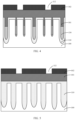
- FIG. 1 is a top view of a substrate according to a first embodiment of the present disclosure.
- FIGS. 2 , 4 , 6 , 8 , 10 , 12 , 14 , 16 , 18 , 20 , 22 and 24 are sectional views taken along AA 1 direction, illustrating structures obtained by implementing various steps of a method for forming a semiconductor structure according to the first embodiment of the present disclosure.
- FIGS. 3 , 5 , 7 , 9 , 11 , 13 , 15 , 17 , 19 , 21 , 23 and 25 are sectional views taken along BB 1 direction, illustrating structures obtained by implementing various steps of a method for forming a semiconductor structure according to the first embodiment of the present disclosure.
- the size of the bit-line structure to be formed decreases, resulting in a decrease in the size of the bit-line contact structure to be formed.
- the decrease in the size of the bit-line contact structure leads to an increase in the contact resistance of the bit-line contact structure, thereby affecting the electrical performance of the subsequently formed semiconductor structure and reducing the yield of the semiconductor structure.
- a first embodiment of the present disclosure provides a method for forming a semiconductor structure.
- the method for forming a semiconductor structure includes: provide a substrate, and form a dielectric layer on a surface of the substrate; form a mask layer on a surface of the dielectric layer, where the mask layer is arranged with a first opening penetrating the mask layer in a thickness direction of the mask layer; form a first barrier layer on a sidewall of the first opening, where the first barrier layer surrounds and forms a second opening; form a second barrier layer filling the second opening; remove the first barrier layer and the second barrier layer by a first etching process until the first barrier layer or the second barrier layer is completely removed, where the removed rate of the first barrier layer by the first etching process is different from the removed rate of the second barrier layer by the first etching process; and remove the dielectric layer exposed by the first opening and part of the substrate exposed by the first opening to form a bit-line contact opening, where the bottom of the bit-line contact opening is arranged with a conve
- FIG. 1 is a top view of a substrate according to the first embodiment of the present disclosure.
- FIGS. 2 , 4 , 6 , 8 , 10 , 12 , 14 , 16 , 18 , 20 , 22 and 24 are sectional views taken along AA 1 direction, illustrating structures obtained by implementing various steps of a method for forming a semiconductor structure according to the first embodiment of the present disclosure.
- FIGS. 3 , 5 , 7 , 9 , 11 , 13 , 15 , 17 , 19 , 21 , 23 and 25 are sectional views taken along BB 1 direction, illustrating structures obtained by implementing various steps of the method for forming a semiconductor structure according to the first embodiment of the present disclosure.
- the method for forming a semiconductor structure according to the first embodiment of the present disclosure is described in further detail below with reference to the drawings.
- the substrate 100 includes shallow trench isolation (STI) structures 110 , active areas 120 and word-line structures 130 .
- STI shallow trench isolation
- the material of the substrate 100 may include silicon, silicon carbide, gallium arsenide, aluminum nitride or zinc oxide, etc.
- the substrate 100 is made of silicon.
- the use of silicon as the substrate 100 in this embodiment is to facilitate the understanding of the subsequent forming method by those skilled in the art, rather than to constitute a limitation. In the actual application process, the appropriate material of the substrate may be selected according to needs.
- Multiple active areas 120 are arranged in parallel and spaced apart in the substrate 100 .
- the substrate 100 is also provided with other memory structures other than the STI structures 110 , the active areas 120 and the word-line structures 130 . Since other memory structures are not related to the core technology of the present disclosure, they are not repeated here. Those skilled in the art may understand that there are other memory structures other than the STI structures 110 , the active areas 120 and the word-line structures 130 in the substrate 100 for normal operation of the memory.
- the method for forming a semiconductor structure provided in this embodiment is described in detail with reference to an AA 1 section and a BB 1 section.
- the AA 1 section is in an extension direction of a bit-line structure
- the BB 1 section is in an extension direction of the word-line structure.
- the word-line structure 130 is a buried word-line structure in the substrate 100 .
- the word-line structure 103 passes through the active areas 120 and the STI structures 110 at intervals.
- the word-line structure 130 is located in the STI structure 110 . It should be noted that in other schematic sectional views of the substrate 100 , the word-line structure 130 may be located in the active area 120 .
- a dielectric layer 101 is formed on a surface of the substrate 100 .
- part of the dielectric layer 101 also covers the word-line structure 130 , which is configured to electrically isolate the word-line structure 130 from a conductive structure on the top of the substrate 100 .
- a mask layer 102 is formed on a surface of the dielectric layer 101 .
- the mask layer 102 is arranged with a first opening 112 penetrating the thickness of the mask layer 102 .
- the mask layer 102 and the first opening 112 are used to define the position of a bit-line contact opening.
- the first opening 112 penetrating the thickness of the mask layer 102 is formed as follows. A patterned photoresist is formed on the top of the mask layer 102 , and the first opening 112 penetrating the thickness of the mask layer 102 is formed according to the patterned photoresist.
- the mask layer 102 has a single-layer structure. In other embodiments, the mask layer may also have a multi-layer structure.
- a first barrier layer 103 is formed on a sidewall of the first opening 112 , and the first barrier layer 103 surrounds and forms a second opening 122 .
- the first barrier layer 103 is formed on the sidewall of the first opening 112 as follows.
- a first barrier film (not shown in the figure) is formed, which covers a top surface of the mask layer 102 and covers the sidewall and bottom of the first opening 112 .
- the first barrier film (not shown in the figure) surrounds and forms the second opening 122 .
- the width of the second opening 122 is less than the width of the first opening 112 in a direction parallel to the surface of the substrate.
- the first barrier film (not shown in the figure) on the top surface of the mask layer 102 and on the bottom of the first opening 112 (not shown in the figure) is removed to form the first barrier layer 103 .
- the first barrier layer 103 is also located on the bottom of the first opening 112 .
- the first barrier layer 103 is formed on the sidewall of the first opening 112 as follows.
- a first barrier film (not shown in the figure) is formed, which covers a top surface of the mask layer 102 and covers the sidewall and bottom of the first opening 112 .
- the first barrier film (not shown in the figure) surrounds and forms the second opening 122 .
- the width of the second opening 122 is less than the width of the first opening 112 in a direction parallel to the surface of the substrate.
- the first barrier film (not shown in the figure) on the top surface of the mask layer 102 is removed to form the first barrier layer 103 .
- the width B of the first barrier layer 103 in the direction parallel to the surface of the substrate 100 is 5 nm to 20 nm, for example, 8 nm, 11 nm, 14 nm or 17 nm. If the width of the first barrier layer 103 is less than 5 nm, the size of a concave region of the bit-line contact opening formed subsequently by etching the first barrier layer 103 may be too small. As a result, when the bit-line contact opening is filled to form the bit-line contact structure, the bit-line contact structure will not be able to completely fill the concave region, thereby leading to a filling defect in the bit-line contact structure.
- the width of the first barrier layer 103 is greater than 20 nm, the size of a second barrier layer formed by filling the gap of the first barrier layer 103 may be too small, which may result in a too small concave region of the bit-line contact opening formed by etching the second barrier layer. Consequently, when the bit-line contact opening is filled to form the bit-line contact structure, the bit-line contact structure will not be able to completely fill the concave region, thereby leading to a defect in the semiconductor structure.
- a second barrier layer 104 filling the second opening 122 (shown in FIG. 6 ) is formed.
- the second barrier layer 104 filling the second opening 122 is formed as follows.
- a second barrier film (not shown in the figure) filling the second opening 122 (shown in FIG. 6 ) and covering the first barrier layer 103 is formed.
- the second barrier film (not shown in the figure) higher than the first barrier layer 103 is removed, and the remaining second barrier film (not shown in the figure) is taken as the second barrier layer 104 .
- the etching selection ratio of the first barrier layer 103 to the second barrier layer 104 is 1:1.1 to 1:3. In another example, the etching selection ratio of the first barrier layer 103 to the second barrier layer 104 is 1.1:1 to 3:1. That is, there is an etching selection ratio of the first barrier layer 103 to the second barrier layer 104 . the etched rate of the first barrier layer 103 is greater than that of the second barrier layer 104 , or the etched rate of the first barrier layer 103 is less than the etched rate of the second barrier layer 104 .
- the first barrier layer 103 and the second barrier layer 104 are removed by a first etching process until the first barrier layer 103 or the second barrier layer 104 is completely removed, where the rate of the first etching process to remove the first barrier layer 103 is different from that to remove the second barrier layer 104 .
- the dielectric layer 101 exposed by the first opening 112 and part of the substrate 100 exposed by the first opening are removed to form a bit-line contact opening 105 , where the bottom of the bit-line contact opening 105 is arranged with a convex region 115 and a concave region 125 , and the convex region 115 and the concave region 125 have a height difference.
- the depth of the bit-line contact opening 105 in a direction perpendicular to the surface of the substrate is 20 nm to 40 nm, for example, 25 nm, 30 nm or 35 nm.
- the convex region 115 and the concave region 125 have a height difference of 1 nm to 15 nm, for example, 3 nm, 5 nm, 7 nm, 9 nm, 11 nm or 13 nm.
- the change of the bottom area of the bit-line contact opening 105 can be controlled.
- the height difference between the convex region 115 and the concave region 125 is less than 1 nm, the increase in the bottom area of the bit-line contact opening 105 is negligible.
- the decrease in the contact resistance of the bit-line contact structure formed by filling the bit-line contact opening 105 is negligible. That is, the contact resistance of the bit-line contact structure is still large, which will affect the electrical performance of the semiconductor structure. If the height difference between the convex region 115 and the concave region 125 is greater than 15 nm, the aspect ratio of the gap between the concave region 125 and the convex region 115 is large. Thus, the bit-line contact structure formed subsequently by filling the bit-line contact opening 105 will not be able to completely fill, which will result in a structural defect, thereby affecting the yield of the semiconductor structure.
- the first barrier layer 103 and the second barrier layer 104 are removed by the first etching process until the first barrier layer 103 or the second barrier layer 104 is completely removed. Specifically, the first barrier layer 103 and the second barrier layer 104 are removed by the first etching process until one of the first barrier layer 103 and the second barrier layer with a faster etched rate is completely removed. Alternatively, the first barrier layer 103 and the second barrier layer 104 are removed by the first etching process until one of the first barrier layer 103 and the second barrier layer 104 with a slower etched rate is completely removed.
- the etched rate of the second barrier layer 104 is greater than that of the first barrier layer 103 .
- the first barrier layer 103 and the second barrier layer 104 are removed by the first etching process until one of the first barrier layer 103 and the second barrier layer 104 with a faster etched rate is completely removed.
- the first barrier layer 103 and the second barrier layer 104 are simultaneously etched by the first etching process.
- the first etching process is stopped. Since the etched rate of the first barrier layer 103 is less than the etched rate of the second barrier layer 104 , part of the first barrier layer 103 remains.
- an etching gas used in the first etching process is a mixed gas which at least includes oxygen and fluorocarbon gas, and the etching time of the first etching process is 20 s to 60 s, for example, 30 s, 40 s or 50 s.
- the first barrier layer 103 or the second barrier layer 104 is etched by a second etching process, and the dielectric layer exposed by the first opening 112 is etched until the substrate 100 is exposed.
- part of the first barrier layer 103 remains after the etching of the first etching process. Therefore, when the second etching process is performed, a middle area on the bottom of the first opening 112 is always lower than an edge area on the bottom of the first opening 112 , until the middle on the bottom of the first opening 112 exposes the substrate 100 . At this time, part of the dielectric layer 101 in the edge area on the bottom of the first opening 112 remains.
- the substrate 100 is etched by a preset thickness by a third etching process to form the bit-line contact opening 105 , wherein the substrate to-be-etched is exposed by the first opening 112 .
- the middle area on the bottom of the first opening 112 is always lower than the edge area on the bottom of the first opening 112 , until the bit-line contact opening 105 is formed.
- the higher area on the bottom forms the convex region 115
- the lower area on the bottom forms the concave region 125 .
- the mask layer 102 is removed.
- the etched rate of the second barrier layer 104 is greater than that of the first barrier layer 103 .
- the above etching example is also applicable to the case where the etched rate of the second barrier layer 104 is less than the etched rate of the first barrier layer 103 .
- the etched rate of the second barrier layer 104 is less than the etched rate of the first barrier layer 103 .
- the first barrier layer 103 and the second barrier layer 104 are removed by the first etching process until one of the first barrier layer 103 and the second barrier layer 104 with a slower etched rate is completely removed.
- the first barrier layer 103 and the second barrier layer 104 are simultaneously etched by the first etching process.
- the first etching process is stopped. Since the etched rate of the first barrier layer 103 is greater than that of the second barrier layer 104 , the dielectric layer 101 on the bottom of the first barrier layer 103 is over-etched. That is, when the first barrier layer 103 and the second barrier layer 104 are removed, part of the dielectric layer 101 is removed, and the etched dielectric layer 101 is located on the bottom of one of the first barrier layer 103 and the second barrier layer 104 with a faster etched rate.
- an etching gas used in the first etching process is a mixed gas which includes at least oxygen and fluorocarbon gas, and the etching time of the first etching process is 20 s to 60 s, for example, 30 s, 40 s or 50 s.
- the dielectric layer 101 exposed by the first opening 112 is etched by the second etching process until the substrate 100 is exposed.
- the second etching process continues to etch the dielectric layer 101 .
- the edge area on the bottom of the first opening 112 is always lower than the middle area on the bottom of the first opening 112 .
- part of the dielectric layer 101 in the middle area on the bottom of the first opening 112 remains.
- the substrate 100 in the edge area on the bottom of the first opening 112 is over-etched.
- the substrate 100 is etched by the third etching process to form the bit-line contact opening 105 , wherein the substrate to-be-etched is exposed by the first opening 112 .
- the substrate 100 in the edge area of the bottom of the first opening 112 is over-etched, when the first opening 112 is etched by the second etching process. Therefore, when the substrate 100 by a preset thickness is etched by the third etching process, the middle area on the bottom of the first opening 112 is always higher than the edge area on the bottom of the first opening 112 , until the bit-line contact opening 105 is formed.
- the higher area on the bottom forms the convex region 115
- the lower area on the bottom forms the concave region 125 .
- the mask layer 102 is removed.
- the etched rate of the second barrier layer 104 is less than the etched rate of the first barrier layer 103 . In other embodiments, the above etching example is also applicable to the case where the etched rate of the second barrier layer 104 is greater than that of the first barrier layer 103 .
- the contact area of the bit-line contact structure formed subsequently is increased. Since the formation area of the word-line structure 130 is not occupied, the performance of the word-line structure 130 will not be affected.
- the bit-line contact opening is arranged with a concave region and a convex region, which increase the bottom area of the bit-line contact opening. In this way, the contact area of the bit-line contact structure formed subsequently by filling the bit-line contact opening is increased, thereby reducing the contact resistance of the bit-line contact structure formed subsequently.
- the semiconductor structure includes: a substrate and a dielectric layer.
- the substrate is arranged with an active area and a first contact opening exposing the active area.
- the bottom of the first contact opening is arranged with a first area and a second area, and the first area and the second area have a height difference.
- the dielectric layer is located on a surface of the substrate.
- the dielectric layer is arranged with a second contact opening penetrating the dielectric layer.
- the second contact opening exposes the first contact opening, and the second contact opening and the first contact opening define a bit-line contact opening.
- FIGS. 18 and 19 are views illustrating the structure of the semiconductor structure provided in this embodiment.
- the semiconductor structure provided in this embodiment is described in detail below with reference to the drawings, and the details the same as or corresponding to those mentioned in the above embodiment will not be repeated here.
- the semiconductor structure includes a substrate 100 and a dielectric layer 101 .
- the substrate 100 is arranged with active areas 120 and first contact openings (not shown in the figure) exposing the active areas 120 .
- the material of the substrate 100 may include silicon, silicon carbide, gallium arsenide, aluminum nitride or zinc oxide, etc.
- the substrate 100 is made of silicon.
- the use of silicon as the substrate 100 in this embodiment is to facilitate the understanding of the subsequent forming method by those skilled in the art, rather than to constitute a limitation. In the actual application process, the appropriate material of the substrate may be selected according to needs.
- Multiple active areas 120 are arranged in parallel and spaced apart in the substrate 100 .
- the substrate 100 is also provided with other memory structures other than STI structures 110 , the active areas 120 and word-line structures 130 . Since other memory structures are not related to the core technology of the present disclosure, they are not repeated here. Those skilled in the art may understand that there are other memory structures other than the STI structures 110 , the active areas 120 and the word-line structures 130 in the substrate 100 for normal operation of the memory.
- the dielectric layer 101 is located on a surface of the substrate 100 .
- the dielectric layer 101 is arranged with a second contact opening (not shown in the figure) penetrating the dielectric layer 101 .
- the second contact opening (not shown in the figure) exposes the first contact opening (not shown in the figure).
- the second contact opening (not shown in the figure) and the first contact opening (not shown in the figure) define a bit-line contact opening 105 .
- the bottom of the first contact opening (not shown in the figure) is arranged with a first area and a second area, and the first area and the second area have a height difference. That is, the bottom of the bit-line contact opening 105 is arranged with a first area and a second area, and the first area and the second area have a height difference.
- the first area is a convex region 115
- the second area is a concave region 125
- the first area surrounds the second area.
- the bottom of the bit-line contact opening 105 includes a first area and a second area with different heights.
- the first area may be a concave region
- the second area may be a convex region.
- the first area and the second area may be spliced on the bottom of the bit-line contact opening.
- the width of the first area in a direction parallel to the surface of the substrate 100 is 5 nm to 20 nm, for example, 8 nm, 11 nm, 14 nm or 17 nm. If the width of the first area is less than 5 nm, the size of the concave region of the bit-line contact opening formed subsequently by etching the first area may be too small. As a result, when the bit-line contact opening is filled to form the bit-line contact structure, the bit-line contact structure will not be able to completely fill the concave region, thereby leading to a filling defect in the bit-line contact structure.
- the width of the first area is greater than 20 nm, the size of a second barrier layer formed by filling the gap of the first area may be too small, which may result in a too small concave region of the bit-line contact opening formed by etching the second barrier layer. Consequently, when the bit-line contact opening is filled to form the bit-line contact structure, the bit-line contact structure will not be able to completely fill the concave region, thereby leading to a defect in the semiconductor structure.
- the depth of the bit-line contact opening 105 is 20 nm to 40 nm, for example, 25 nm, 30 nm or 35 nm; the first area and the second area have a height difference of 1 nm to 15 nm, for example, 3 nm, 5 nm, 7 nm, 9 nm, 11 nm or 13 nm.
- the height difference between the convex region 115 and the concave region 125 is less than 1 nm, the increase in the bottom area of the bit-line contact opening 105 is negligible. Therefore, the decrease in the contact resistance of the bit-line contact structure formed by filling the bit-line contact opening 105 is negligible. That is, the contact resistance of the bit-line contact structure is still large, which will affect the electrical performance of the semiconductor structure. If the height difference between the convex region 115 and the concave region 125 is greater than 15 nm, the aspect ratio of the gap between the concave region 125 and the convex region 115 is large. Thus, the bit-line contact structure formed subsequently by filling the bit-line contact opening 105 will not be able to completely fill, which will result in a structural defect, thereby affecting the yield of the semiconductor structure.
- the contact area of the bit-line contact structure formed subsequently is increased. Since the formation area of the word-line structure 130 is not occupied, the performance of the word-line structure 130 will not be affected.
- the bit-line contact opening is arranged with a concave region and a convex region, which increase the bottom area of the bit-line contact opening. In this way, the contact area of the bit-line contact structure formed subsequently by filling the bit-line contact opening is increased, thereby reducing the contact resistance of the bit-line contact structure formed subsequently.
- this embodiment corresponds to the first embodiment, this embodiment may be implemented in cooperation with the first embodiment.
- the related technical details mentioned in the first embodiment are still valid in this embodiment, and the technical effects that may be achieved in the first embodiment may also be achieved in this embodiment, which will not be repeated here.
- the related technical details mentioned in this embodiment may also be applied to the first embodiment.
- the embodiments of the present disclosure provide a method for forming a semiconductor structure and a semiconductor structure.
- the bit-line contact opening is arranged with a concave region and a convex region on the bottom, which increase the bottom area of the bit-line contact opening. In this way, the contact area of the bit-line contact structure formed subsequently by filling the bit-line contact opening is increased, thereby reducing the contact resistance of the bit-line contact structure formed subsequently.
Landscapes
- Engineering & Computer Science (AREA)
- Manufacturing & Machinery (AREA)
- Physics & Mathematics (AREA)
- Condensed Matter Physics & Semiconductors (AREA)
- General Physics & Mathematics (AREA)
- Computer Hardware Design (AREA)
- Microelectronics & Electronic Packaging (AREA)
- Power Engineering (AREA)
- Internal Circuitry In Semiconductor Integrated Circuit Devices (AREA)
- Geometry (AREA)
Abstract
Description
-
- 100. substrate; 110. shallow trench isolation (STI) structure; 120. active area; 130. word-line structure;
- 101. dielectric layer; 102. mask layer; 103. first barrier layer; 104. second barrier layer; 105. bit-line contact opening; 112. first opening; 122. second opening; 115. convex region; 125. concave region.
Claims (8)
Applications Claiming Priority (3)
| Application Number | Priority Date | Filing Date | Title |
|---|---|---|---|
| CN202110214102.3 | 2021-02-25 | ||
| CN202110214102.3A CN113035868B (en) | 2021-02-25 | 2021-02-25 | Semiconductor structure forming method and semiconductor structure |
| PCT/CN2021/103881 WO2022179028A1 (en) | 2021-02-25 | 2021-06-30 | Semiconductor structure forming method and semiconductor structure |
Publications (2)
| Publication Number | Publication Date |
|---|---|
| US20230402372A1 US20230402372A1 (en) | 2023-12-14 |
| US12205893B2 true US12205893B2 (en) | 2025-01-21 |
Family
ID=76461522
Family Applications (1)
| Application Number | Title | Priority Date | Filing Date |
|---|---|---|---|
| US17/612,546 Active US12205893B2 (en) | 2021-02-25 | 2021-06-30 | Method for forming semiconductor structure and semiconductor structure |
Country Status (3)
| Country | Link |
|---|---|
| US (1) | US12205893B2 (en) |
| CN (1) | CN113035868B (en) |
| WO (1) | WO2022179028A1 (en) |
Families Citing this family (1)
| Publication number | Priority date | Publication date | Assignee | Title |
|---|---|---|---|---|
| CN113035868B (en) * | 2021-02-25 | 2022-05-31 | 长鑫存储技术有限公司 | Semiconductor structure forming method and semiconductor structure |
Citations (6)
| Publication number | Priority date | Publication date | Assignee | Title |
|---|---|---|---|---|
| CN1627504A (en) | 2003-12-12 | 2005-06-15 | 南亚科技股份有限公司 | Method for improving contact resistance value of bit line |
| US20060099786A1 (en) | 2004-10-22 | 2006-05-11 | Taiwan Semiconductor Manufacturing Co. | Copper interconnect structure with modulated topography and method for forming the same |
| US20120007258A1 (en) * | 2010-07-07 | 2012-01-12 | Jae-Geun Oh | Semiconductor device with side-junction and method for fabricating the same |
| US8581337B2 (en) | 2011-11-15 | 2013-11-12 | Hynix Semiconductor Inc. | Semiconductor device for increasing bit line contact area, and module and system including the same |
| CN113035868A (en) | 2021-02-25 | 2021-06-25 | 长鑫存储技术有限公司 | Semiconductor structure forming method and semiconductor structure |
| US20220367667A1 (en) * | 2018-03-01 | 2022-11-17 | Taiwan Semiconductor Manufacturing Co., Ltd. | Contact with a Silicide Region |
Family Cites Families (5)
| Publication number | Priority date | Publication date | Assignee | Title |
|---|---|---|---|---|
| US20090315120A1 (en) * | 2008-06-24 | 2009-12-24 | Lucian Shifren | Raised facet- and non-facet 3d source/drain contacts in mosfets |
| CN108831884A (en) * | 2018-06-08 | 2018-11-16 | 长鑫存储技术有限公司 | Memory structure and its preparation method |
| CN111048467B (en) * | 2018-10-11 | 2024-10-22 | 长鑫存储技术有限公司 | Semiconductor device bit line forming method, semiconductor device |
| CN112242346B (en) * | 2019-07-17 | 2024-12-06 | 长鑫存储技术有限公司 | Semiconductor structure and method for forming the same |
| CN112201580B (en) * | 2020-12-07 | 2021-03-09 | 中芯集成电路制造(绍兴)有限公司 | Contact hole etching method and manufacturing method of semiconductor device |
-
2021
- 2021-02-25 CN CN202110214102.3A patent/CN113035868B/en active Active
- 2021-06-30 WO PCT/CN2021/103881 patent/WO2022179028A1/en not_active Ceased
- 2021-06-30 US US17/612,546 patent/US12205893B2/en active Active
Patent Citations (6)
| Publication number | Priority date | Publication date | Assignee | Title |
|---|---|---|---|---|
| CN1627504A (en) | 2003-12-12 | 2005-06-15 | 南亚科技股份有限公司 | Method for improving contact resistance value of bit line |
| US20060099786A1 (en) | 2004-10-22 | 2006-05-11 | Taiwan Semiconductor Manufacturing Co. | Copper interconnect structure with modulated topography and method for forming the same |
| US20120007258A1 (en) * | 2010-07-07 | 2012-01-12 | Jae-Geun Oh | Semiconductor device with side-junction and method for fabricating the same |
| US8581337B2 (en) | 2011-11-15 | 2013-11-12 | Hynix Semiconductor Inc. | Semiconductor device for increasing bit line contact area, and module and system including the same |
| US20220367667A1 (en) * | 2018-03-01 | 2022-11-17 | Taiwan Semiconductor Manufacturing Co., Ltd. | Contact with a Silicide Region |
| CN113035868A (en) | 2021-02-25 | 2021-06-25 | 长鑫存储技术有限公司 | Semiconductor structure forming method and semiconductor structure |
Non-Patent Citations (1)
| Title |
|---|
| International Search Report in Application No. PCT/CN2021/103881, mailed on Dec. 1, 2021. |
Also Published As
| Publication number | Publication date |
|---|---|
| CN113035868A (en) | 2021-06-25 |
| US20230402372A1 (en) | 2023-12-14 |
| CN113035868B (en) | 2022-05-31 |
| WO2022179028A1 (en) | 2022-09-01 |
Similar Documents
| Publication | Publication Date | Title |
|---|---|---|
| US9613967B1 (en) | Memory device and method of fabricating the same | |
| US20230056204A1 (en) | Semiconductor structure and method for manufacturing same | |
| US12342535B2 (en) | Memory forming method and memory | |
| KR100594279B1 (en) | Method for forming self-aligned contact of semiconductor memory device and manufacturing method of semiconductor memory device using same | |
| CN113192954B (en) | Semiconductor device and manufacturing method thereof | |
| US6093600A (en) | Method of fabricating a dynamic random-access memory device | |
| US12471270B2 (en) | Dynamic random access memory and method of fabricating the same | |
| US12205893B2 (en) | Method for forming semiconductor structure and semiconductor structure | |
| KR100570114B1 (en) | Self Alignment Flush Plate | |
| US7494890B2 (en) | Trench capacitor and method for manufacturing the same | |
| US6303424B1 (en) | Method for fabricating a buried bit line in a DRAM cell | |
| US7638827B2 (en) | Semiconductor memory device | |
| US20220130836A1 (en) | Semiconductor structure formation method and semiconductor structure | |
| US7560370B2 (en) | Method for manufacturing semiconductor device | |
| US6136642A (en) | Method of making a dynamic random access memory | |
| US11956944B2 (en) | DRAM semiconductor structure formation method and DRAM semiconductor structure | |
| US6790740B2 (en) | Process for filling polysilicon seam | |
| KR100546302B1 (en) | Semiconductor device with improved overlap margin and manufacturing method thereof | |
| US11956946B2 (en) | Method for forming a semiconductor memory structure | |
| JPH10209402A (en) | Semiconductor device and manufacturing method thereof | |
| EP3933904B1 (en) | Semiconductor structure and manufacturing method therefor | |
| KR20080069428A (en) | Manufacturing method of semiconductor device | |
| KR100305401B1 (en) | Capacitor Formation Method of Semiconductor Device | |
| CN117790406A (en) | Method for forming semiconductor structure and semiconductor structure | |
| KR960003769B1 (en) | Semiconductor memory device and the manufacturing method |
Legal Events
| Date | Code | Title | Description |
|---|---|---|---|
| AS | Assignment |
Owner name: CHANGXIN MEMORY TECHNOLOGIES, INC., CHINA Free format text: ASSIGNMENT OF ASSIGNORS INTEREST;ASSIGNOR:MU, TIANLEI;REEL/FRAME:058157/0134 Effective date: 20210916 |
|
| FEPP | Fee payment procedure |
Free format text: ENTITY STATUS SET TO UNDISCOUNTED (ORIGINAL EVENT CODE: BIG.); ENTITY STATUS OF PATENT OWNER: LARGE ENTITY |
|
| STPP | Information on status: patent application and granting procedure in general |
Free format text: DOCKETED NEW CASE - READY FOR EXAMINATION |
|
| STPP | Information on status: patent application and granting procedure in general |
Free format text: NON FINAL ACTION MAILED |
|
| STPP | Information on status: patent application and granting procedure in general |
Free format text: RESPONSE TO NON-FINAL OFFICE ACTION ENTERED AND FORWARDED TO EXAMINER |
|
| STPP | Information on status: patent application and granting procedure in general |
Free format text: NON FINAL ACTION MAILED |
|
| STPP | Information on status: patent application and granting procedure in general |
Free format text: FINAL REJECTION MAILED |
|
| STPP | Information on status: patent application and granting procedure in general |
Free format text: NOTICE OF ALLOWANCE MAILED -- APPLICATION RECEIVED IN OFFICE OF PUBLICATIONS |
|
| ZAAB | Notice of allowance mailed |
Free format text: ORIGINAL CODE: MN/=. |
|
| STPP | Information on status: patent application and granting procedure in general |
Free format text: PUBLICATIONS -- ISSUE FEE PAYMENT VERIFIED |
|
| STCF | Information on status: patent grant |
Free format text: PATENTED CASE |