US12205629B2 - Semiconductor-element-including memory device - Google Patents
Semiconductor-element-including memory device Download PDFInfo
- Publication number
- US12205629B2 US12205629B2 US17/968,397 US202217968397A US12205629B2 US 12205629 B2 US12205629 B2 US 12205629B2 US 202217968397 A US202217968397 A US 202217968397A US 12205629 B2 US12205629 B2 US 12205629B2
- Authority
- US
- United States
- Prior art keywords
- layer
- voltage
- gate conductor
- semiconductor
- line
- Prior art date
- Legal status (The legal status is an assumption and is not a legal conclusion. Google has not performed a legal analysis and makes no representation as to the accuracy of the status listed.)
- Active, expires
Links
- 230000015654 memory Effects 0.000 claims abstract description 167
- 239000004020 conductor Substances 0.000 claims abstract description 129
- 239000004065 semiconductor Substances 0.000 claims abstract description 76
- 239000012535 impurity Substances 0.000 claims abstract description 48
- 230000014759 maintenance of location Effects 0.000 claims abstract description 28
- 239000000758 substrate Substances 0.000 claims abstract description 21
- 239000000463 material Substances 0.000 claims description 32
- 239000010410 layer Substances 0.000 description 304
- 238000007667 floating Methods 0.000 description 48
- 230000008878 coupling Effects 0.000 description 34
- 238000010168 coupling process Methods 0.000 description 34
- 238000005859 coupling reaction Methods 0.000 description 34
- 238000010586 diagram Methods 0.000 description 34
- 230000007246 mechanism Effects 0.000 description 21
- 230000006870 function Effects 0.000 description 18
- 230000007423 decrease Effects 0.000 description 12
- 230000008859 change Effects 0.000 description 11
- 239000003990 capacitor Substances 0.000 description 9
- 238000005516 engineering process Methods 0.000 description 9
- 230000014509 gene expression Effects 0.000 description 9
- 230000000694 effects Effects 0.000 description 8
- 230000000717 retained effect Effects 0.000 description 6
- XUIMIQQOPSSXEZ-UHFFFAOYSA-N Silicon Chemical compound [Si] XUIMIQQOPSSXEZ-UHFFFAOYSA-N 0.000 description 3
- 238000013461 design Methods 0.000 description 3
- 239000011159 matrix material Substances 0.000 description 3
- 229910052710 silicon Inorganic materials 0.000 description 3
- 239000010703 silicon Substances 0.000 description 3
- VYPSYNLAJGMNEJ-UHFFFAOYSA-N Silicium dioxide Chemical compound O=[Si]=O VYPSYNLAJGMNEJ-UHFFFAOYSA-N 0.000 description 2
- 239000000969 carrier Substances 0.000 description 2
- 230000000295 complement effect Effects 0.000 description 2
- 230000005684 electric field Effects 0.000 description 2
- 238000012986 modification Methods 0.000 description 2
- 230000004048 modification Effects 0.000 description 2
- 239000002135 nanosheet Substances 0.000 description 2
- 230000008929 regeneration Effects 0.000 description 2
- 238000011069 regeneration method Methods 0.000 description 2
- 101100495436 Saccharomyces cerevisiae (strain ATCC 204508 / S288c) CSE4 gene Proteins 0.000 description 1
- 229910052681 coesite Inorganic materials 0.000 description 1
- 229910052906 cristobalite Inorganic materials 0.000 description 1
- 230000003247 decreasing effect Effects 0.000 description 1
- 238000011161 development Methods 0.000 description 1
- 230000018109 developmental process Effects 0.000 description 1
- 238000010438 heat treatment Methods 0.000 description 1
- 239000012212 insulator Substances 0.000 description 1
- 230000010354 integration Effects 0.000 description 1
- 238000011835 investigation Methods 0.000 description 1
- 238000002955 isolation Methods 0.000 description 1
- 238000000034 method Methods 0.000 description 1
- 238000005457 optimization Methods 0.000 description 1
- 230000008569 process Effects 0.000 description 1
- 238000011160 research Methods 0.000 description 1
- 230000004044 response Effects 0.000 description 1
- 230000000630 rising effect Effects 0.000 description 1
- 229920006395 saturated elastomer Polymers 0.000 description 1
- 239000000377 silicon dioxide Substances 0.000 description 1
- 239000002356 single layer Substances 0.000 description 1
- 229910052682 stishovite Inorganic materials 0.000 description 1
- 238000012546 transfer Methods 0.000 description 1
- 230000007704 transition Effects 0.000 description 1
- 229910052905 tridymite Inorganic materials 0.000 description 1
Images


Classifications
-
- G—PHYSICS
- G11—INFORMATION STORAGE
- G11C—STATIC STORES
- G11C11/00—Digital stores characterised by the use of particular electric or magnetic storage elements; Storage elements therefor
- G11C11/21—Digital stores characterised by the use of particular electric or magnetic storage elements; Storage elements therefor using electric elements
- G11C11/34—Digital stores characterised by the use of particular electric or magnetic storage elements; Storage elements therefor using electric elements using semiconductor devices
- G11C11/40—Digital stores characterised by the use of particular electric or magnetic storage elements; Storage elements therefor using electric elements using semiconductor devices using transistors
- G11C11/401—Digital stores characterised by the use of particular electric or magnetic storage elements; Storage elements therefor using electric elements using semiconductor devices using transistors forming cells needing refreshing or charge regeneration, i.e. dynamic cells
- G11C11/4063—Auxiliary circuits, e.g. for addressing, decoding, driving, writing, sensing or timing
- G11C11/407—Auxiliary circuits, e.g. for addressing, decoding, driving, writing, sensing or timing for memory cells of the field-effect type
- G11C11/409—Read-write [R-W] circuits
- G11C11/4096—Input/output [I/O] data management or control circuits, e.g. reading or writing circuits, I/O drivers or bit-line switches
-
- G—PHYSICS
- G11—INFORMATION STORAGE
- G11C—STATIC STORES
- G11C11/00—Digital stores characterised by the use of particular electric or magnetic storage elements; Storage elements therefor
- G11C11/21—Digital stores characterised by the use of particular electric or magnetic storage elements; Storage elements therefor using electric elements
- G11C11/34—Digital stores characterised by the use of particular electric or magnetic storage elements; Storage elements therefor using electric elements using semiconductor devices
- G11C11/40—Digital stores characterised by the use of particular electric or magnetic storage elements; Storage elements therefor using electric elements using semiconductor devices using transistors
- G11C11/401—Digital stores characterised by the use of particular electric or magnetic storage elements; Storage elements therefor using electric elements using semiconductor devices using transistors forming cells needing refreshing or charge regeneration, i.e. dynamic cells
- G11C11/403—Digital stores characterised by the use of particular electric or magnetic storage elements; Storage elements therefor using electric elements using semiconductor devices using transistors forming cells needing refreshing or charge regeneration, i.e. dynamic cells with charge regeneration common to a multiplicity of memory cells, i.e. external refresh
- G11C11/404—Digital stores characterised by the use of particular electric or magnetic storage elements; Storage elements therefor using electric elements using semiconductor devices using transistors forming cells needing refreshing or charge regeneration, i.e. dynamic cells with charge regeneration common to a multiplicity of memory cells, i.e. external refresh with one charge-transfer gate, e.g. MOS transistor, per cell
-
- G—PHYSICS
- G11—INFORMATION STORAGE
- G11C—STATIC STORES
- G11C11/00—Digital stores characterised by the use of particular electric or magnetic storage elements; Storage elements therefor
- G11C11/21—Digital stores characterised by the use of particular electric or magnetic storage elements; Storage elements therefor using electric elements
- G11C11/34—Digital stores characterised by the use of particular electric or magnetic storage elements; Storage elements therefor using electric elements using semiconductor devices
- G11C11/40—Digital stores characterised by the use of particular electric or magnetic storage elements; Storage elements therefor using electric elements using semiconductor devices using transistors
- G11C11/401—Digital stores characterised by the use of particular electric or magnetic storage elements; Storage elements therefor using electric elements using semiconductor devices using transistors forming cells needing refreshing or charge regeneration, i.e. dynamic cells
- G11C11/4063—Auxiliary circuits, e.g. for addressing, decoding, driving, writing, sensing or timing
- G11C11/407—Auxiliary circuits, e.g. for addressing, decoding, driving, writing, sensing or timing for memory cells of the field-effect type
- G11C11/409—Read-write [R-W] circuits
- G11C11/4094—Bit-line management or control circuits
-
- G—PHYSICS
- G11—INFORMATION STORAGE
- G11C—STATIC STORES
- G11C16/00—Erasable programmable read-only memories
- G11C16/02—Erasable programmable read-only memories electrically programmable
- G11C16/06—Auxiliary circuits, e.g. for writing into memory
- G11C16/24—Bit-line control circuits
-
- H01L29/7827—
-
- H—ELECTRICITY
- H10—SEMICONDUCTOR DEVICES; ELECTRIC SOLID-STATE DEVICES NOT OTHERWISE PROVIDED FOR
- H10B—ELECTRONIC MEMORY DEVICES
- H10B12/00—Dynamic random access memory [DRAM] devices
- H10B12/20—DRAM devices comprising floating-body transistors, e.g. floating-body cells
-
- H—ELECTRICITY
- H10—SEMICONDUCTOR DEVICES; ELECTRIC SOLID-STATE DEVICES NOT OTHERWISE PROVIDED FOR
- H10D—INORGANIC ELECTRIC SEMICONDUCTOR DEVICES
- H10D30/00—Field-effect transistors [FET]
- H10D30/60—Insulated-gate field-effect transistors [IGFET]
- H10D30/63—Vertical IGFETs
-
- G—PHYSICS
- G11—INFORMATION STORAGE
- G11C—STATIC STORES
- G11C2213/00—Indexing scheme relating to G11C13/00 for features not covered by this group
- G11C2213/70—Resistive array aspects
- G11C2213/82—Array having, for accessing a cell, a word line, a bit line and a plate or source line receiving different potentials
-
- G—PHYSICS
- G11—INFORMATION STORAGE
- G11C—STATIC STORES
- G11C7/00—Arrangements for writing information into, or reading information out from, a digital store
- G11C7/10—Input/output [I/O] data interface arrangements, e.g. I/O data control circuits, I/O data buffers
- G11C7/1006—Data managing, e.g. manipulating data before writing or reading out, data bus switches or control circuits therefor
Definitions
- the present invention relates to a semiconductor-element-including memory device.
- Typical planar MOS transistors include a channel that extends in a horizontal direction along the upper surface of the semiconductor substrate.
- SGTs include a channel that extends in a direction perpendicular to the upper surface of the semiconductor substrate (see, for example, Japanese Unexamined Patent Application Publication No. 2-188966 and Hiroshi Takato, Kazumasa Sunouchi, Naoko Okabe, Akihiro Nitayama, Katsuhiko Hieda, Fumio Horiguchi, and Fujio Masuoka: IEEE Transaction on Electron Devices, Vol. 38, No. 3, pp. 573-578 (1991)). Accordingly, the density of semiconductor devices can be made higher with SGTs than with planar MOS transistors.
- Such SGTs can be used as selection transistors to implement highly integrated memories, such as a DRAM (Dynamic Random Access Memory, see, for example, H. Chung, H. Kim, H. Kim, K. Kim, S. Kim, K. Dong, J. Kim, Y. C. Oh, Y. Hwang, H. Hong, G. Jin, and C. Chung: “4F2 DRAM Cell with Vertical Pillar Transistor (VPT)”, 2011 Proceeding of the European Solid-State Device Research Conference, (2011)) to which a capacitor is connected, a PCM (Phase Change Memory, see, for example, H. S. Philip Wong, S. Raoux, S. Kim, Jiale Liang, J. R. Reifenberg, B.
- DRAM Dynamic Random Access Memory
- PCM Phase Change Memory
- FIGS. 7 A to 7 D illustrate a write operation of a DRAM memory cell constituted by a single MOS transistor and including no capacitor described above
- FIGS. 8 A and 8 B illustrate a problem in the operation
- FIGS. 9 A to 9 C illustrate a read operation
- FIG. 7 A illustrates a “1” write state.
- the memory cell is formed on an SOI substrate 100 , is constituted by a source N + layer 103 (hereinafter, a semiconductor region that contains a donor impurity in high concentrations is referred to as “N + layer”) to which a source line SL is connected, a drain N + layer 104 to which a bit line BL is connected, a gate conductor layer 105 to which a word line WL is connected, and a floating body 102 of a MOS transistor 110 , and includes no capacitor.
- the single MOS transistor 110 constitutes the DRAM memory cell. Directly under the floating body 102 , a SiO 2 layer 101 of the SOI substrate is in contact with the floating body 102 .
- the MOS transistor 110 is operated in the saturation region. That is, a channel 107 , for electrons, extending from the source N + layer 103 has a pinch-off point 108 and does not reach the drain N + layer 104 to which the bit line is connected.
- a high voltage is applied to both the bit line BL connected to the drain N + layer and the word line WL connected to the gate conductor layer 105 , and the MOS transistor 110 is operated at the gate voltage that is about one-half of the drain voltage, the electric field intensity becomes maximum at the pinch-off point 108 that is in the vicinity of the drain N + layer 104 .
- FIG. 7 B illustrates a state in which the floating body 102 is charged to saturation with the generated positive holes 106 .
- FIG. 7 C illustrates a state of rewriting from a “1” write state to a “0” write state.
- the voltage of the bit line BL is set to a negative bias, and the PN junction between the drain N + layer 104 and the P-layer floating body 102 is forward biased.
- the positive holes 106 in the floating body 102 generated in advance in the previous cycle flow into the drain N + layer 104 that is connected to the bit line BL.
- the two memory cells are in a state in which the memory cell 110 ( FIG. 7 B ) is filled with the generated positive holes 106 , and from the memory cell 110 ( FIG. 7 C ), the generated positive holes are discharged.
- the potential of the floating body 102 of the memory cell 110 filled with the positive holes 106 becomes higher than that of the floating body 102 in which generated positive holes are not present. Therefore, the threshold voltage for the memory cell 110 to which “1” is written becomes lower than the threshold voltage for the memory cell 110 to which “0” is written. This is illustrated in FIG. 7 D .
- the capacitance C FB of the floating body is equal to the sum of the capacitance C WL between the gate to which the word line is connected and the floating body, the junction capacitance C SL of the PN junction between the source N + layer 103 to which the source line is connected and the floating body 102 , and the junction capacitance C BL of the PN junction between the drain N + layer 104 to which the bit line is connected and the floating body 102 and is expressed as follows.
- C FB C WL +C BL +C SL (14)
- ⁇ WL C WL /( C WL +C BL +C SL ) (15)
- a change in the word line voltage V WL at the time of reading or writing affects the voltage of the floating body 102 that functions as a storage node (contact point) of the memory cell. This is illustrated in FIG. 8 B .
- the voltage V FB of the floating body 102 rises from V FB1 , which is the voltage in the initial state before the word line voltage changes, to V FB2 due to capacitive coupling with the word line.
- FIGS. 9 A to 9 C illustrate a read operation where FIG. 9 A illustrates a “1” write state and FIG. 9 B illustrates a “0” write state.
- Vb is set for the floating body 102 to write “1”
- the floating body 102 is lowered to a negative bias.
- the floating body 102 is lowered to a further negative bias, and it is difficult to provide a sufficiently large margin to the potential difference between “1” and “0” at the time of writing as illustrated in FIG. 9 C . Therefore, there has been difficulty in commercially introducing DRAM memory cells actually including no capacitor.
- capacitor-less single-transistor DRAMs of a memory device
- capacitive coupling between the word line and the floating body is strong.
- the potential of the word line is changed at the time of data reading or at the time of data writing, the change is directly transmitted to the floating body as noise, which is a problem.
- This causes a problem of erroneous reading or erroneous rewriting of storage data and makes it difficult to commercially introduce capacitor-less single-transistor DRAMs (gain cells).
- a semiconductor-element-including memory device is a memory device, the memory device including a plurality of pages arranged in a column direction, each of the pages being constituted by a plurality of memory cells arranged in a row direction on a substrate, each of the memory cells included in each of the pages including: a semiconductor base material that stands on the substrate in a vertical direction or that extends along the substrate in a horizontal direction; a first impurity layer and a second impurity layer that are disposed at respective ends of the semiconductor base material; a first gate insulating layer that partially or entirely surrounds a side surface of the semiconductor base material between the first impurity layer and the second impurity layer and that is in contact with or in close vicinity to the first impurity layer; a second gate insulating layer that surrounds the side surface of the semiconductor base material, that is connected to the first gate insulating layer, and that is in contact with or in close vicinity to the second impurity layer; a first gate insulating layer that partially or entirely surrounds a side surface of
- a first gate capacitance between the first gate conductor layer and the channel semiconductor layer is larger than a second gate capacitance between the second gate conductor layer and the channel semiconductor layer (second invention).
- the first gate conductor layer is isolated into at least two conductor layers around the first gate insulating layer when viewed in an axial direction of the semiconductor base material (third invention).
- the impact ionization phenomenon occurs inside the channel semiconductor layer between the first gate conductor layer and the second gate conductor layer to generate the group of positive holes inside the channel semiconductor layer (fourth invention).
- a semiconductor-element-including memory device includes a group of blocks each including the plurality of pages of the semiconductor-element-including memory device according to any one of the first to fourth inventions described above, in which the first impurity layer is connected to a source line, the second impurity layer is connected to a bit line, one of the first gate conductor layer or the second gate conductor layer is connected to a word line, the other of the first gate conductor layer or the second gate conductor layer is connected to a first driving control line, and the word line and the first driving control line are connected to a row decoder circuit, the source line is connected to the semiconductor base materials in each block in the group of blocks, and voltages applied to the source line, the bit line, the first driving control line, and the word line are controlled to perform either the memory re-write operation or the memory re-erase operation or simultaneously perform both the memory re-write operation and the memory re-erase operation for all the semiconductor base materials in a block selected from among the group of blocks (fifth invention).
- an all-word-line selection signal and an all-plate-line selection signal are input to the row decoder circuit to select all the word lines and all the plate lines in the block (sixth invention).
- a first driving control line is disposed so as to be shared among the memory cells adjacent to each other (seventh invention).
- the source line is isolated into source lines each of which is for the memory cells that are arranged in the column direction and which are disposed parallel to the word lines and the plate lines (eighth invention).
- the first refresh operation and the second refresh operation are performed in advance at least once for the word lines selected in multiple selection in the page sum-of-products read operation (ninth invention).
- FIG. 1 is a structural diagram of an SGT-including memory device according to a first embodiment
- FIGS. 2 A to 2 C are diagrams for explaining an effect attained in a case where the gate capacitance of a first gate conductor layer connected to a plate line is made larger than the gate capacitance of a second gate conductor layer to which a word line is connected in the SGT-including memory device according to the first embodiment;
- FIGS. 3 AA to 3 AC are diagrams for explaining a mechanism of a write operation of the SGT-including memory device according to the first embodiment
- FIG. 3 B includes diagrams for explaining the mechanism of the write operation of the SGT-including memory device according to the first embodiment
- FIG. 4 A is a diagram for explaining a mechanism of a page erase operation of the SGT-including memory device according to the first embodiment
- FIGS. 4 BA to 4 BD are diagrams for explaining the mechanism of the page erase operation of the SGT-including memory device according to the first embodiment
- FIG. 4 C includes diagrams for explaining the mechanism of the page erase operation of the SGT-including memory device according to the first embodiment
- FIGS. 4 DA to 4 DD are diagrams for explaining a mechanism of the page erase operation of the SGT-including memory device according to the first embodiment
- FIGS. 4 EA to 4 ED are diagrams for explaining a mechanism of the page erase operation of the SGT-including memory device according to the first embodiment
- FIGS. 5 A to 5 C are diagrams for explaining a mechanism of a read operation of the SGT-including memory device according to the first embodiment
- FIGS. 6 AA and 6 AB are diagrams for explaining a first refresh operation of the SGT-including memory device according to the first embodiment
- FIG. 6 B is an operation waveform diagram for explaining the first refresh operation of the SGT-including memory device according to the first embodiment
- FIGS. 6 CA and 6 CB are diagrams for explaining a second refresh operation of the SGT-including memory device according to the first embodiment
- FIG. 6 D is an operation waveform diagram for explaining the second refresh operation of the SGT-including memory device according to the first embodiment
- FIG. 6 E is a circuit block diagram for explaining the first refresh operation and the second refresh operation of the SGT-including memory device according to the first embodiment
- FIG. 6 F is a circuit block diagram for explaining the first refresh operation and the second refresh operation of the SGT-including memory device according to the first embodiment
- FIG. 6 G is a circuit block diagram for explaining the first refresh operation of the SGT-including memory device according to the first embodiment
- FIG. 6 H is a circuit block diagram for explaining the second refresh operation of the SGT-including memory device according to the first embodiment
- FIG. 6 I is a circuit block diagram for explaining the first refresh operation and the second refresh operation of the SGT-including memory device according to the first embodiment
- FIG. 6 J is a circuit block diagram for explaining the first refresh operation and the second refresh operation of the SGT-including memory device according to the first embodiment
- FIGS. 7 A to 7 D are diagrams for explaining a write operation of a DRAM memory cell including no capacitor in the related art
- FIGS. 8 A and 8 B are diagrams for explaining a problem in the operation of the DRAM memory cell including no capacitor in the related art.
- FIGS. 9 A to 9 C are diagrams for explaining a read operation of the DRAM memory cell including no capacitor in the related art.
- a semiconductor-element-including memory device hereinafter called a dynamic flash memory
- FIG. 1 The structure and operation mechanisms of a dynamic flash memory cell according to a first embodiment of the present invention will be described with reference to FIG. 1 to FIGS. 5 A to 5 C .
- the structure of the dynamic flash memory cell will be described with reference to FIG. 1 .
- An effect attained in a case where the gate capacitance of a first gate conductor layer 5 a connected to a plate line PL is made larger than the gate capacitance of a second gate conductor layer 5 b to which a word line WL is connected will be described with reference to FIGS. 2 A to 2 C .
- a mechanism of a data write operation will be described with reference to FIGS. 3 AA to 3 AC and FIG. 3 B
- mechanisms of a data erase operation will be described with reference to FIG. 4 A to FIGS. 4 EA to 4 ED
- a mechanism of a data read operation will be described with reference to FIGS. 5 A to 5 C .
- FIG. 1 illustrates the structure of the dynamic flash memory cell according to the first embodiment of the present invention.
- Si pillar which is an example of “semiconductor base material” in the claims
- N + layers 3 a and 3 b which are examples of “first impurity layer” and “second impurity layer” in the claims, one of which functions as the source and the other functions as the drain, are formed respectively.
- the part of the Si pillar 2 between the N + layers 3 a and 3 b that function as the source and the drain functions as a channel region 7 (which is an example of “channel semiconductor layer” in the claims).
- a first gate insulating layer 4 a (which is an example of “first gate insulating layer” in the claims) and a second gate insulating layer 4 b (which is an example of “second gate insulating layer” in the claims) are formed.
- the first gate insulating layer 4 a and the second gate insulating layer 4 b are in contact with or in close vicinity to the N + layers 3 a and 3 b that function as the source and the drain respectively.
- the first gate conductor layer 5 a (which is an example of “first gate conductor layer” in the claims) and the second gate conductor layer 5 b (which is an example of “second gate conductor layer” in the claims) are formed respectively.
- the first gate conductor layer 5 a and the second gate conductor layer 5 b are isolated from each other by an insulating layer 6 (which is also referred to as “first insulating layer”).
- the channel region 7 between the N + layers 3 a and 3 b is constituted by a first channel Si layer 7 a surrounded by the first gate insulating layer 4 a and a second channel Si layer 7 b surrounded by the second gate insulating layer 4 b . Accordingly, the N + layers 3 a and 3 b that function as the source and the drain, the channel region 7 , the first gate insulating layer 4 a , the second gate insulating layer 4 b , the first gate conductor layer 5 a , and the second gate conductor layer 5 b constitute a dynamic flash memory cell 10 .
- the N + layer 3 a that functions as the source is connected to a source line SL (which is an example of “source line” in the claims), the N + layer 3 b that functions as the drain is connected to a bit line BL (which is an example of “bit line” in the claims), the first gate conductor layer 5 a is connected to the plate line PL (which is an example of “first driving control line” in the claims), and the second gate conductor layer 5 b is connected to the word line WL (which is an example of “word line” in the claims).
- the structure is such that the gate capacitance of the first gate conductor layer 5 a to which the plate line PL is connected is larger than the gate capacitance of the second gate conductor layer 5 b to which the word line WL is connected.
- the gate length of the first gate conductor layer 5 a is made longer than the gate length of the second gate conductor layer 5 b .
- the thicknesses of the respective gate insulating layers may be made different such that the thickness of the gate insulating film of the first gate insulating layer 4 a is thinner than the thickness of the gate insulating film of the second gate insulating layer 4 b .
- the dielectric constants of the materials of the respective gate insulating layers may be made different such that the dielectric constant of the gate insulating film of the first gate insulating layer 4 a is higher than the dielectric constant of the gate insulating film of the second gate insulating layer 4 b .
- the gate capacitance of the first gate conductor layer 5 a connected to the plate line PL may be made larger than the gate capacitance of the second gate conductor layer 5 b to which the word line WL is connected, by a combination of any of the lengths of the gate conductor layers 5 a and 5 b and the thicknesses and dielectric constants of the gate insulating layers 4 a and 4 b.
- FIGS. 2 A to 2 C are diagrams for explaining an effect attained in a case where the gate capacitance of the first gate conductor layer 5 a connected to the plate line PL is made larger than the gate capacitance of the second gate conductor layer 5 b to which the word line WL is connected.
- FIG. 2 A is a simplified structural diagram of the dynamic flash memory cell according to the first embodiment of the present invention and illustrates only main parts.
- the bit line BL, the word line WL, the plate line PL, and the source line SL are connected, and the potential state of the channel region 7 is determined by the voltage states of the lines.
- FIG. 2 B is a diagram for explaining the capacitance relationships of the respective lines.
- the capacitance C FB of the channel region 7 is equal to the sum of the capacitance C WL between the gate conductor layer 5 b to which the word line WL is connected and the channel region 7 , the capacitance C PL between the gate conductor layer 5 a to which the plate line PL is connected and the channel region 7 , the junction capacitance C SL of the PN junction between the source N + layer 3 a to which the source line SL is connected and the channel region 7 , and the junction capacitance C BL of the PN junction between the drain N + layer 3 b to which the bit line BL is connected and the channel region 7 , and is expressed as follows.
- C FB C WL +C PL +C BL +C SL (1)
- the coupling ratio ⁇ WL between the word line WL and the channel region 7 the coupling ratio ⁇ FL between the plate line PL and the channel region 7 , the coupling ratio ⁇ BL between the bit line BL and the channel region 7 , and the coupling ratio ⁇ SL between the source line SL and the channel region 7 are expressed as follows.
- FIG. 2 C is a diagram for explaining a change in the voltage V FB of the channel region 7 when the voltage V WL of the word line WL rises at the time of a read operation or a write operation and subsequently drops.
- the potential difference ⁇ V FB when the voltage V FB of the channel region 7 transitions from a low-voltage state V FBL to a high-voltage state V FBH in response to the voltage V WL of the word line WL rising from 0 V to a high-voltage state V WLH is expressed as follows.
- the coupling ratio ⁇ WL between the word line WL and the channel region 7 is small and the coupling ratio ⁇ FL between the plate line PL and the channel region 7 is large, and therefore, ⁇ V FB is small, and the voltage V FB of the channel region 7 negligibly changes even when the voltage V WL of the word line WL changes at the time of a read operation or a write operation.
- FIGS. 3 AA to 3 AC and FIG. 3 B illustrate a memory write operation (which is an example of “page write operation” in the claims) of the dynamic flash memory cell according to the first embodiment of the present invention.
- FIG. 3 AA illustrates a mechanism of the write operation
- FIG. 3 AB illustrates operation waveforms of the bit line BL, the source line SL, the plate line PL, the word line WL, and the channel region 7 that functions as a floating body FB.
- the dynamic flash memory cell is in a “0” erase state, and the voltage of the channel region 7 is equal to V FB “0”.
- Vss is applied to the bit line BL, the source line SL, and the word line WL, and V PLL is applied to the plate line PL.
- Vss is equal to 0 V and V PLL is equal to 2 V.
- Vss is equal to 0 V
- V PLL is equal to 2 V.
- the word line WL rises from Vss to V WLH . Accordingly, when the threshold voltage for “0” erase for a second N-channel MOS transistor region that is a region in which the second gate conductor layer 5 b to which the word line WL is connected surrounds the channel region 7 is denoted by Vt WL “0”, as the voltage of the word line WL rises, in a range from Vss to Vt WL “0”, the voltage of the channel region 7 becomes equal to V FB “0”+ ⁇ BL ⁇ V BLH + ⁇ WL ⁇ Vt WL “0” due to second capacitive coupling between the word line WL and the channel region 7 .
- an inversion layer 12 b in a ring form is formed in the channel region 7 on the inner periphery of the second gate conductor layer 5 b and interrupts the second capacitive coupling between the word line WL and the channel region 7 .
- a first N-channel MOS transistor region including the first gate conductor layer 5 a operates in the saturation region.
- the second N-channel MOS transistor region including the second gate conductor layer 5 b to which the word line WL is connected operates in the linear region.
- a pinch-off point is not present in the channel region 7 on the inner periphery of the second gate conductor layer 5 b to which the word line WL is connected, and the inversion layer 12 b is formed on the entire inner periphery of the gate conductor layer 5 b .
- the inversion layer 12 b that is formed on the entire inner periphery of the second gate conductor layer 5 b to which the word line WL is connected substantially functions as the drain of the second N-channel MOS transistor region including the second gate conductor layer 5 b .
- the electric field becomes maximum in a first boundary region of the channel region 7 between the first N-channel MOS transistor region including the first gate conductor layer 5 a and the second N-channel MOS transistor region including the second gate conductor layer 5 b that are connected in series, and an impact ionization phenomenon occurs in this region.
- This region is a source-side region when viewed from the second N-channel MOS transistor region including the second gate conductor layer 5 b to which the word line WL is connected, and therefore, this phenomenon is called a source-side impact ionization phenomenon.
- This source-side impact ionization phenomenon electrons flow from the N + layer 3 a to which the source line SL is connected toward the N + layer 3 b to which the bit line is connected.
- the accelerated electrons collide with lattice Si atoms, and electron-positive hole pairs are generated by the kinetic energy. Although some of the generated electrons flow into the first gate conductor layer 5 a and into the second gate conductor layer 5 b , most of the generated electrons flow into the N + layer 3 b to which the bit line BL is connected (not illustrated).
- a generated group of positive holes 9 are majority carriers in the channel region 7 , with which the channel region 7 is charged to a positive bias.
- the N + layer 3 a to which the source line SL is connected is at 0 V, and therefore, the channel region 7 is charged up to the built-in voltage Vb (about 0.7 V) of the PN junction between the N + layer 3 a to which the source line SL is connected and the channel region 7 .
- Vb about 0.7 V
- the capacitive coupling between the word line WL and the channel region 7 is substantially formed only during a period from when the word line WL drops to Vt W L “1” or below to when the word line WL drops to Vss.
- the voltage of the channel region 7 becomes equal to Vb ⁇ WL ⁇ Vt WL “1”.
- Vt WL “1” is lower than Vt WL “0” described above, and ⁇ WL ⁇ Vt WL “1” is small.
- the coupling ratio ⁇ BL between the bit line BL and the channel region 7 is also small. Accordingly, as illustrated in FIG. 3 B , the threshold voltage for the second N-channel MOS transistor region of the second channel region 7 b to which the word line WL is connected decreases.
- electron-positive hole pairs may be generated by an impact ionization phenomenon in a second boundary region between the first impurity layer 3 a and the first channel semiconductor layer 7 a or in a third boundary region between the second impurity layer 3 b and the second channel semiconductor layer 7 b instead of the first boundary region, and the channel region 7 may be charged with the generated group of positive holes 9 .
- the conditions of voltages applied to the bit line BL, the source line SL, the word line WL, and the plate line PL and the potential of the floating body described above are examples for performing the write operation, and other operation conditions based on which the write operation can be performed may be employed.
- a mechanism of a memory erase operation (which is an example of “page erase operation” in the claims) will be described with reference to FIG. 4 A to FIGS. 4 EA to 4 ED .
- FIG. 4 A is a memory block circuit diagram for explaining a page erase operation. Although nine memory cells CL 11 to CL 33 in three rows and three columns are illustrated, the actual memory block is larger than this matrix.
- the source line SL, a corresponding one of the bit lines BL 1 to BL 3 , a corresponding one of the plate lines PL 1 to PL 3 , and a corresponding one of the word lines WL 1 to WL 3 are connected.
- FIG. 4 BA is a timing operation waveform diagram of main nodes in the erase operation.
- T0 to T12 indicate times from the start to the end of the erase operation.
- FIG. 4 BB illustrates a state at time T0 before the erase operation, in which the group of positive holes 9 generated by an impact ionization phenomenon in the previous cycle are stored in the channel region 7 .
- bit lines BL 1 to BL 3 and the source line SL rise from Vss to V BLH and V SLH respectively and are in a high-voltage state.
- Vss is, for example, equal to 0 V.
- the plate line PL 2 selected in the page erase operation rises from a first voltage V PLL to a second voltage V PLH and is in a high-voltage state
- the word line WL 2 selected in the page erase operation rises from a third voltage Vss to a fourth voltage V WLH and is in a high-voltage state, and this prevents the inversion layer 12 a on the inner periphery of the first gate conductor layer 5 a to which the plate line PL 2 is connected and the inversion layer 12 b on the inner periphery of the second gate conductor layer 5 b to which the word line WL 2 is connected from being formed in the channel region 7 .
- V tWL and V tPL the threshold voltage for the second N-channel MOS transistor region on the side of the word line WL 2 and the threshold voltage for the first N-channel MOS transistor region on the side of the plate line PL 2
- V tWL and V tPL the threshold voltage for the second N-channel MOS transistor region on the side of the word line WL 2
- V tPL and V tPL the threshold voltage for the first N-channel MOS transistor region on the side of the plate line PL 2
- This voltage rise is possible because the voltage of the bit lines BL 1 to BL 3 and that of the source line SL are high voltages of V BLH and V SLH respectively and the PN junction between the source N + layer 3 a and the channel region 7 and the PN junction between the drain N + layer 3 b and the channel region 7 are in a reverse bias state accordingly.
- the voltage V FB of the channel region 7 becomes equal to the built-in voltage Vb of the PN junction formed by the source N + layer 3 a and the P-layer channel region 7 and the PN junction formed by the drain N + layer 3 b and the P-layer channel region 7 .
- the voltage V FB of the channel region 7 efficiently changes from Vb to V FB “0” due to the first capacitive coupling between the plate line PL 2 and the channel region 7 and the second capacitive coupling between the word line WL 2 and the channel region 7 without the inversion layer 12 a on the side of the plate line PL 2 or the inversion layer 12 b on the side of the word line WL 2 being formed in the channel region 7 .
- the voltage difference ⁇ V FB of the channel region 7 between the “1” write state and the “0” erase state is expressed by the following expressions.
- V FB ⁇ “ 1 ” Vb - ⁇ W ⁇ L ⁇ V ⁇ t W ⁇ L ⁇ “ 1 ” - ⁇ B ⁇ L ⁇ V BLH ( 7 )
- V F ⁇ B ⁇ “ 0 ” Vb - ⁇ W ⁇ L ⁇ V WLH - ⁇ P ⁇ L ⁇ ( V PLH - V PLL ) ( 8 )
- the sum of ⁇ WL and ⁇ PL is greater than or equal to 0.8, ⁇ V FB is large, and a sufficient margin is provided.
- the threshold voltage on the side of the plate line PL 2 is high due to a substrate bias effect. Therefore, when the voltage applied to the plate line PL 2 is set to, for example, the threshold voltage or lower, the first N-channel MOS transistor region on the side of the plate line PL 2 becomes non-conducting and does not allow the memory cell current to flow therethrough. This state is illustrated in the right part of FIG. 4 C and indicated as “PL: non-conducting”.
- FIGS. 4 DA to 4 DD are different from FIGS. 4 BA to 4 BD in that the bit lines BL 1 to BL 3 are kept at Vss or put in a floating state and the word line WL 2 is kept at Vss during the page erase operation. Accordingly, from time T1 to time T2, even when the source line SL rises from Vss to V SLH , the second N-channel MOS transistor region of the word line WL 2 is non-conducting, and the memory cell current does not flow therethrough. Therefore, the group of positive holes 9 caused by an impact ionization phenomenon are not generated. The others are the same as in FIGS.
- the source line SL changes between Vss and V SLH
- the plate line PL 2 changes between V PLL and V PLH .
- the group of positive holes 9 are discharged to the first impurity layer, namely, the N + layer 3 a , of the source line SL.
- FIGS. 4 EA to FIG. 4 ED are different from FIGS. 4 BA to 4 BD in that the source line SL is kept at Vss or put in a floating state and the plate line PL 2 is kept at Vss during the page erase operation. Accordingly, from time T1 to time T2, even when the bit lines BL 1 to BL 3 rise from Vss to V BLH , the first N-channel MOS transistor region of the plate line PL 2 is non-conducting, and the memory cell current does not flow therethrough. Therefore, the group of positive holes 9 caused by an impact ionization phenomenon are not generated.
- FIGS. 4 BA to 4 BD The others are the same as in FIGS. 4 BA to 4 BD , and the bit lines BL 1 to BL 3 change between Vss and V BLH , and the word line WL 2 changes between Vss and V WLH .
- the group of positive holes 9 are discharged to the second impurity layer, namely, the N + layer 3 b , of the bit lines BL 1 to BL 3 .
- the conditions of voltages applied to the bit line BL, the source line SL, the word line WL, and the plate line PL and the potential of the floating body described above are examples for performing the page erase operation, and other operation conditions based on which the page erase operation can be performed may be employed.
- FIGS. 5 A to 5 C are diagrams for explaining a read operation of the dynamic flash memory cell according to the first embodiment of the present invention.
- Vb built-in voltage
- the threshold voltage for the second N-channel MOS transistor region including the second gate conductor layer 5 b to which the word line WL is connected decreases due to a substrate bias effect.
- This state is assigned to logical storage data “1”.
- FIG. 5 B a memory block selected before writing is in an erase state “0” in advance, and the voltage V FB of the channel region 7 is equal to V FB “0”. With a write operation, a write state “1” is stored at random.
- logical storage data of logical “0” and that of logical “1” are created for the word line WL.
- the level difference between the two threshold voltages of the word line WL is used to perform reading by a sense amplifier.
- the voltage applied to the first gate conductor layer 5 a connected to the plate line PL is set to a voltage higher than the threshold voltage at the time of logical storage data “1” and lower than the threshold voltage at the time of logical storage data “0” in logical “0” data reading, a property that a current does not flow even when the voltage of the word line WL is increased can be attained as illustrated in FIG. 5 C .
- the conditions of voltages applied to the bit line BL, the source line SL, the word line WL, and the plate line PL and the potential of the floating body described above are examples for performing the read operation, and other operation conditions based on which the read operation can be performed may be employed.
- FIGS. 6 AA and 6 AB and FIG. 6 B are diagrams for explaining a first refresh operation (which is an example of “first refresh operation” in the claims) for a “0” erase state of the dynamic flash memory cell according to the first embodiment of the present invention.
- FIG. 6 AA illustrates a single dynamic flash memory cell in a “0” erase state.
- the initial voltage of the channel region 7 to which “0” is written is equal to V FB “0” at a first time (which is an example of “first time” in the claims)
- FIG. 6 AB illustrates four dynamic flash memory cells CL00 to CL03 that constitute a part of the same page.
- the dynamic flash memory cells CL00 and CL03 are in a “1” write state and an excessive group of positive holes 9 are retained in the channel region 7
- the dynamic flash memory cells CL01 and CL02 are in a “0” erase state, and no excessive group of positive holes 9 are retained in the channel region 7 but a small group of positive holes 9 have entered the channel region 7 due to, for example, a leak current.
- a positive-bias pulse is applied to the word line WL and to the plate line PL while the bit lines BL 0 to BL 3 and the source line SL are kept at Vss.
- Vss is equal to, for example, 0 V.
- FIG. 6 B which illustrates changes in the voltages of the bit line BL, the source line SL, the word line WL, the plate line PL, and the channel region 7 that functions as the floating body FB, over time from time T0 to time T2.
- the PN junction between the P-layer channel region 7 and the source N + layer 3 a and the PN junction between the P-layer channel region 7 and the drain N + layer 3 b are forward biased, and the group of positive holes 9 having flowed into the channel region 7 are discharged to the source N + layer 3 a and to the drain N + layer 3 b .
- the inversion layer 12 a is formed in the channel region 7 surrounded by the first gate conductor layer 5 a to which the plate line PL is connected and the inversion layer 12 b is formed in the channel region 7 surrounded by the second gate conductor layer 5 b to which the word line WL is connected.
- Both the bit line BL and the source line SL are kept at Vss, and therefore, a current does not flow from the bit line BL to the source line SL or an impact ionization phenomenon does not occur.
- the inversion layers 12 a and 12 b shield the first gate conductor layer 5 a and the second gate conductor layer 5 b from the channel region 7 , and therefore, the voltage of the channel region 7 does not rise.
- the threshold voltage Vt WL “0” for the second N-channel MOS transistor region that is a region in which the second gate conductor layer 5 b surrounds the channel layer 7 increases from that in the “0” erase state at the second time before the first refresh operation.
- FIGS. 6 CA and 6 CB and FIG. 6 D are diagrams for explaining a second refresh operation (which is an example of “second refresh operation” in the claims) for a “1” write state of the dynamic flash memory cell according to the first embodiment of the present invention.
- FIG. 6 CA illustrates a single dynamic flash memory cell constituted by a single semiconductor base material and in a “1” write state.
- the initial voltage of the channel region 7 to which “1” is written is equal to V FB “1”
- FIG. 6 CB illustrates the four dynamic flash memory cells CL00 to CL03 that constitute a part of the same page in which a plurality of semiconductor base materials are arranged.
- the dynamic flash memory cells CL00 and CL03 are in a “1” write state at the first time and an excessive group of positive holes 9 are retained in the channel region 7 .
- the dynamic flash memory cells CL01 and CL02 are in a “0” erase state and no excessive group of positive holes 9 are retained in the channel region 7 .
- a positive bias is applied to the bit lines BL 0 to BL 3 , to the word line WL, and to the plate line PL and the source line SL is kept at Vss.
- Vss is equal to, for example, 0 V. Specific examples of the operation waveforms are illustrated in FIG.
- V BLR is a voltage of the bit line BL for a refresh operation of a block to which “1” is written and is equal to, for example, 2 V.
- V WLRP is a voltage applied to the word line WL for a refresh operation of a block to which “1” is written and is equal to, for example, 4 V.
- the first N-channel MOS transistor region that is a region in which the first gate conductor layer 5 a to which the plate line PL is connected surrounds the channel region 7 operates in the saturation region
- the second N-channel MOS transistor region that is a region in which the second gate conductor layer 5 b to which the word line WL is connected surrounds the channel layer 7 operates in the linear region. Accordingly, a current flows from the drain N + layer 3 b to the source N + layer 3 a , and the group of positive holes 9 are generated by an impact ionization phenomenon, with which the channel region 7 is filled.
- the voltage of the channel region 7 becomes equal to the built-in voltage Vb (about 0.7 V).
- the threshold voltage Vt PL “0” in the “0” erase state of the first N-channel MOS transistor region that is a region in which the first gate conductor layer 5 a to which the plate line PL is connected surrounds the channel layer 7
- the threshold voltage Vt WL “0” in the “0” erase state of the second N-channel MOS transistor region that is a region in which the second gate conductor layer 5 b to which the word line WL is connected surrounds the channel layer 7 are high, and therefore, a current does not flow from the drain N + layer 3 b to the source N + layer 3 a at time T2 or an impact ionization phenomenon does not occur.
- the description of the second refresh operation for the “1” write state of the dynamic flash memory cell according to the first embodiment of the present invention will be continued with reference to FIG. 6 D .
- the word line WL drops from V WLRP to Vss.
- the inversion layer 12 b is generated in the channel layer 7 surrounded by the second gate conductor layer 5 b to which the word line WL is connected, and this inversion layer interrupts second capacitive coupling between the second gate conductor layer 5 b and the channel layer 7 .
- Vt WL “1” When the threshold voltage in the “1” write state of the second N-channel MOS transistor region that is a region in which the second gate conductor layer 5 b surrounds the channel layer 7 is denoted by Vt WL “1”, the second capacitive coupling between the second gate conductor layer 5 b and the channel layer 7 works when the voltage of the word line WL drops to Vt WL “1” or below, and the voltage of the channel region 7 becomes equal to Vb1 expressed by expression (12).
- Vb 1 Vb ⁇ WL ⁇ Vt WL “1” (12)
- Vt WL “1” in the “1” write state is low, and therefore, ⁇ WL ⁇ Vt WL “1” is small.
- the bit line BL drops from V BLR to Vss, and the second refresh operation for the “1” write state ends.
- the voltage V FB “1” of the channel region 7 becomes equal to Vb2 at the end expressed by expression (13).
- the threshold voltage Vt WL for the second N-channel MOS transistor region that is a region in which the second gate conductor layer 5 b surrounds the channel layer 7 decreases from that in the “1” write state before the second refresh operation.
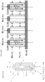
- memory cells C00 to C22 in three rows and three columns constitute a part of a block (which is an example of “block” in the claims). Although the memory cells C00 to C22 in three rows and three columns are illustrated here, memory cells in a matrix larger than three rows and three columns constitute the actual block.
- a corresponding one of the word lines WL0 to WL2 a corresponding one of the plate lines PL0 to PL2, the source line SL, and a corresponding one of the bit lines BL0 to BL2 are connected.
- Transistors T0C to T2C each having a gate to which a transfer signal FT is input constitute a switch circuit.
- the drains of transistors T0D to T2D each having a gate connected to a bit line pre-charge signal FS are connected to a bit line power VB, and the sources thereof are connected to the bit lines BL0 to BL2 respectively.
- the bit lines BL0 to BL2 are respectively connected to sense amplifier circuits SA0 to SA2 with the switch circuit therebetween.
- the word lines WL0 to WL2 and the plate lines PL0 to PL2 are connected to a row decoder circuit RDEC.
- the sense amplifier circuits SA0 to SA2 are connected to a pair of complementary input/output lines IO and/IO, with transistors T0A to T2B each having a gate connected to a corresponding one of the column selection lines CSL0 to CSL2 therebetween.
- FIG. 6 F is a circuit block diagram illustrating a state in which, at a certain timing, “1” is written to the memory cells C10, C01, C21, C02, and C12 at random among the memory cells C00 to C22 and the group of positive holes 9 are stored in the channel semiconductor layer 7 of each of the memory cells.
- the first refresh operation related to all word lines WL and all plate lines PL in the block will be described with reference to FIG. 6 G .
- FIG. 6 G illustrates a case where an all-word-line selection signal ALLWL (which is an example of “all-word-line selection signal” in the claims) and an all-plate-line selection signal ALLPL (which is an example of “all-plate-line selection signal” in the claims) are input to the row decoder circuit.
- ALLWL which is an example of “all-word-line selection signal” in the claims
- ALLPL which is an example of “all-plate-line selection signal” in the claims
- a state in which all the word lines WL0 to WL2 in the memory cell block are selected and the memory cells C10, C01, C21, C02, and C12 are subjected to the first refresh operation is illustrated.
- the memory cells C00, C11, C20, and C22 in FIG. 6 G are in a “0” erase state and no excessive group of positive holes 9 are retained in the channel region 7 , a small group of positive holes 9 entered the channel region 7 at the second time due to, for example, a leak current.
- a positive-bias pulse is applied to the word lines WL and to the plate lines PL while the bit lines BL0 to BL2 and the source line SL are kept at Vss.
- Vss is equal to, for example, 0 V.
- the group of positive holes 9 having entered the channel region 7 due to, for example, a leak current are discharged to the bit lines BL0 to BL2 and to the source line SL.
- the voltage of the channel region 7 of each of the memory cells C00, C11, C20, and C22 in the “0” erase state returns to a voltage close to the second data retention voltage.
- the second refresh operation related to all word lines WL and all plate lines PL in the block will be described with reference to FIG. 6 H .
- a refresh operation of generating by an impact ionization phenomenon, the group of positive holes 9 inside the channel semiconductor layer 7 of each of the memory cells C10, C01, C21, C02, and C12 to which “1” is written in FIG. 6 H is performed.
- the threshold voltage of the first gate conductor layer 5 a and that of the second gate conductor layer 5 b of each of the memory cells C10, C01, C21, C02, and C12 decrease, for example, from 1.3 V in the “0” erase state to 0.3 V in the “1” write state, that is, decrease by 1 V.
- the first refresh operation and the second refresh operation related to all word lines WL and all plate lines PL in the memory cell block illustrated in FIG. 6 G and FIG. 6 H are very effective for a page sum-of-products read operation (which is an example of “page sum-of-products read operation” in the claims) in which at least two word lines are selected in multiple selection.
- the page sum-of-products read operation for example, the three word lines WL0 to WL2 in FIG. 6 F are selected in multiple selection.
- Memory cell currents Icell are added up for each of the bit lines BL0 to BL2, and therefore, as the memory cell currents, saturated and stable memory cell currents need to be read. Therefore, the first refresh operation and the second refresh operation related to all word lines WL and all plate lines PL in the memory cell block in FIG. 6 G and FIG. 6 H performed before the page sum-of-products read operation are very effective.
- FIG. 6 I illustrates an example where the plate line PL is shared among adjacent memory cells in the block constituted by the memory cells C00 to C22 in three rows and three columns.
- the first refresh operation and the second refresh operation of the dynamic flash memory cell according to the first embodiment of the present invention can also be performed before page reading.
- FIG. 6 J illustrates an example where isolated source lines, namely, a source line SL0 parallel to the plate line PL0 and the word line WL0, a source line SL1 parallel to the plate line PL1 and the word line WL1, and a source line SL2 parallel to the plate line PL2 and the word line WL2, are disposed in the block constituted by the memory cells C00 to C22 in three rows and three columns.
- the first refresh operation and the second refresh operation of the dynamic flash memory cell according to the first embodiment of the present invention can also be performed before page reading.
- the operations of the dynamic flash memory described in this embodiment can be performed. Further, a dynamic flash memory cell having a round shape, a dynamic flash memory cell having an elliptic shape, and a dynamic flash memory cell having a rectangular shape may coexist on the same chip.
- the dynamic flash memory element including, for example, an SGT in which the first gate insulating layer 4 a and the second gate insulating layer 4 b that surround the entire side surface of the Si pillar 2 standing on the substrate in the vertical direction are provided and which includes the first gate conductor layer 5 a and the second gate conductor layer 5 b that entirely surround the first gate insulating layer 4 a and the second gate insulating layer 4 b has been described.
- the dynamic flash memory element needs to have a structure that satisfies the condition that the group of positive holes 9 generated by an impact ionization phenomenon are retained in the channel region 7 .
- the channel region 7 needs to have a floating body structure isolated from the substrate.
- GAA Gate All Around
- SGT Standard Gas Source Electron Device
- the dynamic flash memory element may have a device structure using SOI (Silicon On Insulator) (see, for example, J. Wan, L. Rojer, A. Zaslaysky, and S. Critoloveanu: “A Compact Capacitor-Less High-Speed DRAM Using Field Effect-Controlled Charge Regeneration”, Electron Device Letters, Vol. 35, No. 2, pp. 179-181 (2012), T. Ohsawa, K.
- SOI Silicon On Insulator
- the bottom portion of the channel region is in contact with an insulating layer of the SOI substrate, and the other portion of the channel region is surrounded by a gate insulating layer and an element isolation insulating layer. With such a structure, the channel region also has a floating body structure.
- the dynamic flash memory element provided in this embodiment needs to satisfy the condition that the channel region has a floating body structure.
- a Fin transistor see, for example, H. Jiang, N. Xu, B. Chen, L. Zeng 1, Y. He, G. Du, X. Liu and X. Zhang: “Experimental investigation of self-heating effect (SHE) in multiple-fin SOI FinFETs”, Semicond. Sci. Technol. 29 (2014) 115021 (7pp)
- SHE self-heating effect
- Expressions (1) to (13) provided in the specification and in the drawings are expressions used to qualitatively explain the phenomena, and are not intended to limit the phenomena.
- the reset voltages of the word line WL, the bit line BL, and the source line SL are specified as Vss in the explanations of FIGS. 3 AA to 3 AC and FIG. 3 B , the reset voltages of the respective lies may be set to different voltages.
- FIG. 4 BA , FIG. 4 DA , and FIG. 4 EA and the descriptions thereof illustrate example conditions of the page erase operation
- the voltages applied to the source line SL, the plate line PL, the bit line BL, and the word line WL may be changed as long as a state in which the group of positive holes 9 in the channel region 7 are discharged through either the N + layer 3 a or the N + layer 3 b or both the N + layer 3 a and the N + layer 3 b can be attained.
- a voltage may be applied to the source line SL of a selected page, and the bit line BL may be put in a floating state.
- a voltage may be applied to the bit line BL of a selected page, and the source line SL may be put in a floating state.
- the potential distribution of the first channel region 7 a and that of the second channel region 7 b are connected and formed. Accordingly, the first channel region 7 a and the second channel region 7 b that constitute the channel region 7 are connected in the vertical direction in the region surrounded by the insulating layer 6 that is the first insulating layer.
- any voltage conditions may be employed as long as an impact ionization phenomenon can be made to occur inside the channel region 7 with a memory cell current and the refresh operation of generating the group of positive holes 9 can be performed.
- V PLL of the plate line PL a fixed voltage of, for example, about 1 V may be applied.
- the meaning of “cover” in a case of “for example, a gate insulating layer or a gate conductor layer covers, for example, a channel” also includes a case of surrounding entirely as in an SGT or GAA, a case of surrounding except a portion as in a Fin transistor, and a case of overlapping a flat object as in a planar transistor.
- first gate conductor layer 5 a entirely surrounds the first gate insulating layer 4 a in FIG. 1
- a structure may be employed in which the first gate conductor layer 5 a partially surrounds the first gate insulating layer 4 a in plan view.
- the first gate conductor layer 5 a may be divided into at least two gate conductor layers and each of which may be operated as a plate line PL electrode.
- the second gate conductor layer 5 b may be divided into two or more gate conductor layers, and the gate conductor layers may each function as a conductive electrode of the word line and may be operated synchronously or asynchronously. Accordingly, the operations of the dynamic flash memory can be performed.
- the first gate conductor layer 5 a may be connected to the word line WL, and the second gate conductor layer 5 b may be connected to the plate line PL.
- the operations of the dynamic flash memory described above can also be performed.
- the present invention is also effective for the refresh operations of a one-bit high-speed dynamic flash memory cell constituted by two semiconductor base materials that store complementary data of “1” and “0”.
- the present invention is also effective for a multilayer memory array including one-bit dynamic flash memory cells stacked in multiple tiers and each constituted by a single semiconductor base material.
- This embodiment has the following features.
- the dynamic flash memory cell of this embodiment is constituted by the N + layers 3 a and 3 b that function as the source and the drain, the channel region 7 , the first gate insulating layer 4 a , the second gate insulating layer 4 b , the first gate conductor layer 5 a , and the second gate conductor layer 5 b , which are formed in a pillar form as a whole.
- the N + layer 3 a that functions as the source is connected to the source line SL
- the N + layer 3 b that functions as the drain is connected to the bit line BL
- the first gate conductor layer 5 a is connected to the plate line PL
- the second gate conductor layer 5 b is connected to the word line WL.
- a structure is employed in which the gate capacitance of the first gate conductor layer 5 a to which the plate line PL is connected is larger than the gate capacitance of the second gate conductor layer 5 b to which the word line WL is connected, which is a feature.
- the first gate conductor layer and the second gate conductor layer are stacked in the vertical direction. Accordingly, even when the structure is employed in which the gate capacitance of the first gate conductor layer 5 a to which the plate line PL is connected is larger than the gate capacitance of the second gate conductor layer 5 b to which the word line WL is connected, the memory cell area does not increase in plan view. Accordingly, a high-performance and highly integrated dynamic flash memory cell can be implemented.
- the first refresh operation of the dynamic flash memory cell according to the first embodiment of the present invention is performed prior to the second refresh operation.
- the channel region 7 in a floating state is made to change to a large degree by using the word line WL and the plate line PL and the group of positive holes 9 having flowed into the channel region 7 due to, for example, a leak current are discharged to the source N + layer 3 a and to the drain N + layer 3 b .
- inversion layers are formed in the channel region 7 and the inversion layers interrupt capacitive coupling between the word line WL and the channel region 7 and between the plate line PL and the channel region 7 .
- the voltage of the word line WL changes.
- the plate line PL assumes the role of decreasing the capacitive coupling ratio between the word line WL and the channel region 7 .
- an effect on changes in the voltage of the channel region 7 when the voltage of the word line WL changes can be substantially suppressed.
- the difference between the threshold voltages for the SGT transistors of the word line WL indicating logical “0” and logical “1” can be increased. This leads to an increased operation margin of the dynamic flash memory cell.
- the Si pillar is formed in the present invention
- the Si pillar may be a semiconductor pillar made of a semiconductor material other than Si. This is similarly applicable to other embodiments according to the present invention.
Landscapes
- Engineering & Computer Science (AREA)
- Microelectronics & Electronic Packaging (AREA)
- Computer Hardware Design (AREA)
- Databases & Information Systems (AREA)
- Dram (AREA)
- Semiconductor Memories (AREA)
Abstract
Description
C FB =C WL +C BL +C SL (14)
βWL =C WL/(C WL +C BL +C SL) (15)
ΔV FB =V FB2 −V FB1=βWL ×V WLH (16)
C FB =C WL +C PL +C BL +C SL (1)
βWL =C WL/(C WL +C PL +C BL +C SL) (2)
βPL =C PL/(C WL +C PL +C BL +C SL) (3)
βBL =C BL/(C WL +C PL +C BL +C SL) (4)
βSL =C SL/(C WL +C PL +C BL +C SL) (5)
ΔV FB =V FBH −V FBL=βWL ×V WLH (6)
V FB“1”=Vb−β WL ×Vt WL“1”−βBL ×V BLH (7)
V FB“0”=Vb−β WL ×V WLRE−βPL×(V PLR −V PLL) (10)
βBL =C BL/(C WL +C PL +C BL +C SL) (4)
V FB2 =V FB1+βBL ×V BLR (11)
Vb1=Vb−β WL ×Vt WL“1” (12)
V FB“1”=Vb2=Vb1−βBL ×V BLR =Vb−β WL ×Vt WL“1”−βBL ×V BLR (13)
Claims (9)
Applications Claiming Priority (3)
| Application Number | Priority Date | Filing Date | Title |
|---|---|---|---|
| WOPCT/JP2021/038588 | 2021-10-19 | ||
| PCT/JP2021/038588 WO2023067686A1 (en) | 2021-10-19 | 2021-10-19 | Memory device using semiconductor element |
| JPPCT/JP2021/038588 | 2021-10-19 |
Publications (2)
| Publication Number | Publication Date |
|---|---|
| US20230120181A1 US20230120181A1 (en) | 2023-04-20 |
| US12205629B2 true US12205629B2 (en) | 2025-01-21 |
Family
ID=85981996
Family Applications (1)
| Application Number | Title | Priority Date | Filing Date |
|---|---|---|---|
| US17/968,397 Active 2043-04-18 US12205629B2 (en) | 2021-10-19 | 2022-10-18 | Semiconductor-element-including memory device |
Country Status (3)
| Country | Link |
|---|---|
| US (1) | US12205629B2 (en) |
| TW (1) | TWI818770B (en) |
| WO (1) | WO2023067686A1 (en) |
Cited By (3)
| Publication number | Priority date | Publication date | Assignee | Title |
|---|---|---|---|---|
| US12315570B2 (en) * | 2021-01-29 | 2025-05-27 | Unisantis Electronics Singapore Pte. Ltd. | Semiconductor element memory device |
| US12362006B2 (en) * | 2022-06-14 | 2025-07-15 | Unisantis Electronics Singapore Pte. Ltd. | Semiconductor-element-including memory device |
| US12419032B2 (en) * | 2022-12-20 | 2025-09-16 | Unisantis Electronics Singapore Pte. Ltd. | Memory device including semiconductor element |
Families Citing this family (2)
| Publication number | Priority date | Publication date | Assignee | Title |
|---|---|---|---|---|
| WO2022219694A1 (en) * | 2021-04-13 | 2022-10-20 | ユニサンティス エレクトロニクス シンガポール プライベート リミテッド | Memory device using semiconductor element |
| CN118265288A (en) * | 2022-12-26 | 2024-06-28 | 长江存储科技有限责任公司 | Memory device and method for forming a memory device |
Citations (10)
| Publication number | Priority date | Publication date | Assignee | Title |
|---|---|---|---|---|
| JPH02188966A (en) | 1989-01-17 | 1990-07-25 | Toshiba Corp | Mos semiconductor device |
| JPH03171768A (en) | 1989-11-30 | 1991-07-25 | Toshiba Corp | Semiconductor storage device |
| US20030111681A1 (en) | 2001-12-14 | 2003-06-19 | Kabushiki Kaisha Toshiba | Semiconductor memory device and its manufacturing method |
| US20060049444A1 (en) | 2004-09-09 | 2006-03-09 | Kabushiki Kaisha Toshiba | Semiconductor device and method of fabricating the same |
| JP3957774B2 (en) | 1995-06-23 | 2007-08-15 | 株式会社東芝 | Semiconductor device |
| US20080137394A1 (en) | 2006-12-12 | 2008-06-12 | Renesas Technology Corp. | Semiconductor memory device |
| US20080212366A1 (en) | 2007-03-01 | 2008-09-04 | Kabushiki Kaisha Toshiba | Semiconductor memory device |
| JP7057032B1 (en) * | 2020-12-25 | 2022-04-19 | ユニサンティス エレクトロニクス シンガポール プライベート リミテッド | Memory device using semiconductor elements |
| US20230039991A1 (en) * | 2021-08-03 | 2023-02-09 | Unisantis Electronics Singapore Pte. Ltd. | Memory device using semiconductor element |
| US20230046352A1 (en) * | 2021-08-10 | 2023-02-16 | Unisantis Electronics Singapore Pte. Ltd. | Method of producing semiconductor device including memory element |
Family Cites Families (2)
| Publication number | Priority date | Publication date | Assignee | Title |
|---|---|---|---|---|
| JP2009093708A (en) * | 2007-10-04 | 2009-04-30 | Toshiba Corp | Semiconductor memory device and driving method thereof |
| JP2010157580A (en) * | 2008-12-26 | 2010-07-15 | Toshiba Corp | Semiconductor memory device |
-
2021
- 2021-10-19 WO PCT/JP2021/038588 patent/WO2023067686A1/en not_active Ceased
-
2022
- 2022-10-18 TW TW111139487A patent/TWI818770B/en active
- 2022-10-18 US US17/968,397 patent/US12205629B2/en active Active
Patent Citations (15)
| Publication number | Priority date | Publication date | Assignee | Title |
|---|---|---|---|---|
| JPH02188966A (en) | 1989-01-17 | 1990-07-25 | Toshiba Corp | Mos semiconductor device |
| JPH03171768A (en) | 1989-11-30 | 1991-07-25 | Toshiba Corp | Semiconductor storage device |
| JP3957774B2 (en) | 1995-06-23 | 2007-08-15 | 株式会社東芝 | Semiconductor device |
| US20060157738A1 (en) | 2001-12-14 | 2006-07-20 | Kabushiki Kaisha Toshiba | Semiconductor memory device and its manufacturing method |
| JP2003188279A (en) | 2001-12-14 | 2003-07-04 | Toshiba Corp | Semiconductor memory device and method of manufacturing the same |
| US20030111681A1 (en) | 2001-12-14 | 2003-06-19 | Kabushiki Kaisha Toshiba | Semiconductor memory device and its manufacturing method |
| US20060049444A1 (en) | 2004-09-09 | 2006-03-09 | Kabushiki Kaisha Toshiba | Semiconductor device and method of fabricating the same |
| JP2006080280A (en) | 2004-09-09 | 2006-03-23 | Toshiba Corp | Semiconductor device and manufacturing method thereof |
| US20080137394A1 (en) | 2006-12-12 | 2008-06-12 | Renesas Technology Corp. | Semiconductor memory device |
| JP2008147514A (en) | 2006-12-12 | 2008-06-26 | Renesas Technology Corp | Semiconductor memory device |
| US20080212366A1 (en) | 2007-03-01 | 2008-09-04 | Kabushiki Kaisha Toshiba | Semiconductor memory device |
| JP2008218556A (en) | 2007-03-01 | 2008-09-18 | Toshiba Corp | Semiconductor memory device |
| JP7057032B1 (en) * | 2020-12-25 | 2022-04-19 | ユニサンティス エレクトロニクス シンガポール プライベート リミテッド | Memory device using semiconductor elements |
| US20230039991A1 (en) * | 2021-08-03 | 2023-02-09 | Unisantis Electronics Singapore Pte. Ltd. | Memory device using semiconductor element |
| US20230046352A1 (en) * | 2021-08-10 | 2023-02-16 | Unisantis Electronics Singapore Pte. Ltd. | Method of producing semiconductor device including memory element |
Non-Patent Citations (18)
| Title |
|---|
| E. Yoshida and T. Tanaka: "A Design of a Capacitorless 1T-DRAM Cell Using Gate-induced Drain Leakage (GIDL) Current for Low-power and High-speed Embedded Memory," IEEE IEDM, pp. 913-916, Dec. 2003. |
| E. Yoshida, and T. Tanaka: "A Capacitorless 1T-DRAM Technology Using Gate-Induced Dran-Leakage (GIDL) Currect for Low-Power and High-Speed Embedded Memory," IEEE Transactions on Electron Devices, vol. 53, No. 4, pp. 692-697, Apr. 2006. |
| English translation of International Search Report (PCT/ISA/210) from PCT/JP2021/038588 dated Dec. 7, 2021, 2 pgs. |
| F. Morishita, H. Noda, I. Hayashi, T. Gyohten, M. Oksmoto, T. Ipposhi, S. Maegawa, K. Dosaka, and K. Arimoto: "Capacitorless Twin-Transistor Random Access Memory (TTRAM) on SOI", IEICE Trans. Electron., vol. E90-C, No. 4 pp. 765-771 (2007). |
| H. Chung, H. Kim, H. Kim, K. Kim, S. Kim, K. W. Song, J. Kim, Y. C. Oh, Y. Hwang, H. Hong, G. Jin, and C. Chung: "Novel 4F2 Dram Cell with Vertical Pillar Transistor (VPT)," 2011 Proceeding of the European Solid-State Device Research Conference, (2011). |
| H. Jiang, N. Xu, B. Chen, L. Zeng, Y. He, G. Du, X. Liu and X. Zhang: "Experimental investigation of self heating effect (SHE) in multiple-fin SOI FinFETs," Semicond. Sci. Technol. 29 (2014) 115021, 9 pgs. |
| H. S. Philip Wong, S. Raoux, S. Kim, Jiale Liang, J. P. Reifenberg, B. Rajendran, M. Asheghi and K. E. Goodson: "Phase Change Memory," Proceeding of IEEE, vol. 98, No. 12, Dec., pp. 2201-2227 (2010). |
| Hiroshi Takato, Kazumasa Sunouchi, Naoko Okabe, Akihiro Nitayama, Katsuhiko Hieda, Fumio Horiguchi, and Fujio Masuoka "Impact of Surrounding Gate Transistor (SGT) for Ultra-High Density LSI's", IEEE Transaction on Electron Devices, vol. 38, No. 3, pp. 573-578 (1991). |
| International Search Report (PCT/ISA/210) (Japanese) from PCT/JP2021/038588 dated Dec. 7, 2021, 4 pgs. See translation identified as A29. |
| International Written Opinion (PCT/ISA/137) (Japanese) from PCT/JP2021/038588 dated Dec. 7, 2021, 3 pgs. |
| J. Wan, L. Rojer, A. Zaslavsky, and S. Critoloveanu: "A Compact Capacitor-Less High-Speed DRAM Using Field Effect-Controlled Charge Regeneration," Electron Device Letters, vol. 35, No. 2, pp. 179-181 (2012). |
| J. Y. Song, W. Y. Choi, J. H. Park, J. D. Lee, and B-G. Park: "Design Optimization of Gate-All-Around (GAA) MOSFETs," IEEE Trans. Electron Devices, vol. 5, No. 3, pp. 186-191, May 2006. |
| K. Tsunoda, K. Kinoshita, H. Noshiro, Y. Yamazaki, T. Iizuka, Y. Ito, A. Takahashi, A. Okano, Y. Sato, T. Fukano, M. Aoki, and Y. Sugiyama: "Low Power and High Spped Switching of Ti-doped NiO ReRAM under the Unipolar Voltage Source of less than 3V," IEDM (2007) pp. 767-770. |
| M. G. Ertosun, K. Lim, C. Park, J. Oh, P. Kirsch, and K. C. Saraswat: "Novel Capacitorless Single-Transistor Charge-Trap DRAM (1T CT DRAM) Utilizing Electron," IEEE Electron Device Letter, vol. 31, No. 5, pp. 405-407 (2010). |
| N. Loubet, et al.: "Stacked Nanosheet Gate-All-Around Transistor to Enable Scaling Beyond FinFET," 2017 IEEE Symposium on VLSI Technology Digest of Technical Papers, T17-5, T230-T231, Jun. 2017. |
| T. Ohsawa, K. Fujita, T. Higashi, Y. Iwata, T. Kajiyama, Y. Asao, and K. Sunouchi, "Memory design using a one-transistor gain cell on SOI," IEEE JSSC, vol. 37, No. 11, pp. 1510-1522 (2002). |
| T. Shino, N. Kusunoki, T. Higashi, T. Ohsawa, K. Fujita, K. Hatsuda, N. Ikumi, F. Matsuoka, Y. Kajitani, R. Fukuda, Y. Watanabe, Y. Minami, A. Sakamoto, J. Nishimura, H. Nakajima, M. Morikado, K. Inoh, T. Hamamoto, A. Nitayama: "Floating Body RAM Technology and its Scalability to 32nm Node and Beyond," IEEE IEDM 4 pgs. (2006). |
| W. Kang, L. Zhang, J. Klein, Y. Zhang, D. Ravelosona, and W. Zhao: "Reconfigurable Codesign of STT-MRAM Under Process Variations in Deeply Scaled Technology," IEEE Transaction on Electron Devices, pp. 1-9 (2015). |
Cited By (3)
| Publication number | Priority date | Publication date | Assignee | Title |
|---|---|---|---|---|
| US12315570B2 (en) * | 2021-01-29 | 2025-05-27 | Unisantis Electronics Singapore Pte. Ltd. | Semiconductor element memory device |
| US12362006B2 (en) * | 2022-06-14 | 2025-07-15 | Unisantis Electronics Singapore Pte. Ltd. | Semiconductor-element-including memory device |
| US12419032B2 (en) * | 2022-12-20 | 2025-09-16 | Unisantis Electronics Singapore Pte. Ltd. | Memory device including semiconductor element |
Also Published As
| Publication number | Publication date |
|---|---|
| WO2023067686A1 (en) | 2023-04-27 |
| TW202327028A (en) | 2023-07-01 |
| US20230120181A1 (en) | 2023-04-20 |
| TWI818770B (en) | 2023-10-11 |
Similar Documents
| Publication | Publication Date | Title |
|---|---|---|
| US12131773B2 (en) | Memory device | |
| US12100443B2 (en) | Semiconductor-element-including memory device | |
| US11996136B2 (en) | Semiconductor-element-including memory device | |
| US12205629B2 (en) | Semiconductor-element-including memory device | |
| US11823727B2 (en) | Semiconductor element memory device | |
| WO2023281613A1 (en) | Memory device using semiconductor element | |
| US12315570B2 (en) | Semiconductor element memory device | |
| US12185522B2 (en) | Memory apparatus using semiconductor devices | |
| US12277962B2 (en) | Memory device using semiconductor element | |
| US20220328488A1 (en) | Semiconductor element memory device | |
| US12245417B2 (en) | Semiconductor-element-including memory device | |
| US20220328089A1 (en) | Semiconductor element memory device | |
| WO2022269740A1 (en) | Memory device using semiconductor element | |
| US12166107B2 (en) | Semiconductor-element-including memory device | |
| TWI807874B (en) | Memory device using semiconductor elements | |
| WO2022269737A1 (en) | Memory device using semiconductor element | |
| US11937418B2 (en) | Semiconductor-element-including memory device | |
| US12376284B2 (en) | Memory device using dynamic flash memory cells | |
| WO2022172318A1 (en) | Memory device using semiconductor element | |
| US12367923B2 (en) | Semiconductor element memory device | |
| US12249366B2 (en) | Semiconductor-element-including memory device | |
| US20230038107A1 (en) | Memory device using semiconductor element | |
| WO2024062539A1 (en) | Memory device using semiconductor element | |
| WO2024053014A1 (en) | Memory device using semiconductor element | |
| US12362006B2 (en) | Semiconductor-element-including memory device |
Legal Events
| Date | Code | Title | Description |
|---|---|---|---|
| AS | Assignment |
Owner name: UNISANTIS ELECTRONICS SINGAPORE PTE., SINGAPORE Free format text: ASSIGNMENT OF ASSIGNORS INTEREST;ASSIGNORS:SAKUI, KOJI;HARADA, NOZOMU;REEL/FRAME:061460/0313 Effective date: 20221012 |
|
| FEPP | Fee payment procedure |
Free format text: ENTITY STATUS SET TO UNDISCOUNTED (ORIGINAL EVENT CODE: BIG.); ENTITY STATUS OF PATENT OWNER: SMALL ENTITY |
|
| FEPP | Fee payment procedure |
Free format text: ENTITY STATUS SET TO SMALL (ORIGINAL EVENT CODE: SMAL); ENTITY STATUS OF PATENT OWNER: SMALL ENTITY |
|
| STPP | Information on status: patent application and granting procedure in general |
Free format text: DOCKETED NEW CASE - READY FOR EXAMINATION |
|
| STPP | Information on status: patent application and granting procedure in general |
Free format text: NON FINAL ACTION MAILED |
|
| STPP | Information on status: patent application and granting procedure in general |
Free format text: RESPONSE TO NON-FINAL OFFICE ACTION ENTERED AND FORWARDED TO EXAMINER |
|
| STPP | Information on status: patent application and granting procedure in general |
Free format text: NOTICE OF ALLOWANCE MAILED -- APPLICATION RECEIVED IN OFFICE OF PUBLICATIONS |
|
| ZAAB | Notice of allowance mailed |
Free format text: ORIGINAL CODE: MN/=. |
|
| STPP | Information on status: patent application and granting procedure in general |
Free format text: PUBLICATIONS -- ISSUE FEE PAYMENT VERIFIED |
|
| STCF | Information on status: patent grant |
Free format text: PATENTED CASE |