US12204220B2 - Display device and display system - Google Patents
Display device and display system Download PDFInfo
- Publication number
- US12204220B2 US12204220B2 US17/942,250 US202217942250A US12204220B2 US 12204220 B2 US12204220 B2 US 12204220B2 US 202217942250 A US202217942250 A US 202217942250A US 12204220 B2 US12204220 B2 US 12204220B2
- Authority
- US
- United States
- Prior art keywords
- layer
- switch electrode
- display device
- insulating layer
- liquid crystal
- Prior art date
- Legal status (The legal status is an assumption and is not a legal conclusion. Google has not performed a legal analysis and makes no representation as to the accuracy of the status listed.)
- Active, expires
Links
Images


Classifications
-
- H—ELECTRICITY
- H10—SEMICONDUCTOR DEVICES; ELECTRIC SOLID-STATE DEVICES NOT OTHERWISE PROVIDED FOR
- H10K—ORGANIC ELECTRIC SOLID-STATE DEVICES
- H10K50/00—Organic light-emitting devices
- H10K50/80—Constructional details
- H10K50/85—Arrangements for extracting light from the devices
-
- G—PHYSICS
- G02—OPTICS
- G02F—OPTICAL DEVICES OR ARRANGEMENTS FOR THE CONTROL OF LIGHT BY MODIFICATION OF THE OPTICAL PROPERTIES OF THE MEDIA OF THE ELEMENTS INVOLVED THEREIN; NON-LINEAR OPTICS; FREQUENCY-CHANGING OF LIGHT; OPTICAL LOGIC ELEMENTS; OPTICAL ANALOGUE/DIGITAL CONVERTERS
- G02F1/00—Devices or arrangements for the control of the intensity, colour, phase, polarisation or direction of light arriving from an independent light source, e.g. switching, gating or modulating; Non-linear optics
- G02F1/01—Devices or arrangements for the control of the intensity, colour, phase, polarisation or direction of light arriving from an independent light source, e.g. switching, gating or modulating; Non-linear optics for the control of the intensity, phase, polarisation or colour
- G02F1/13—Devices or arrangements for the control of the intensity, colour, phase, polarisation or direction of light arriving from an independent light source, e.g. switching, gating or modulating; Non-linear optics for the control of the intensity, phase, polarisation or colour based on liquid crystals, e.g. single liquid crystal display cells
- G02F1/133—Constructional arrangements; Operation of liquid crystal cells; Circuit arrangements
- G02F1/1333—Constructional arrangements; Manufacturing methods
-
- G—PHYSICS
- G02—OPTICS
- G02B—OPTICAL ELEMENTS, SYSTEMS OR APPARATUS
- G02B30/00—Optical systems or apparatus for producing three-dimensional [3D] effects, e.g. stereoscopic images
- G02B30/20—Optical systems or apparatus for producing three-dimensional [3D] effects, e.g. stereoscopic images by providing first and second parallax images to an observer's left and right eyes
- G02B30/22—Optical systems or apparatus for producing three-dimensional [3D] effects, e.g. stereoscopic images by providing first and second parallax images to an observer's left and right eyes of the stereoscopic type
- G02B30/24—Optical systems or apparatus for producing three-dimensional [3D] effects, e.g. stereoscopic images by providing first and second parallax images to an observer's left and right eyes of the stereoscopic type involving temporal multiplexing, e.g. using sequentially activated left and right shutters
-
- G—PHYSICS
- G02—OPTICS
- G02B—OPTICAL ELEMENTS, SYSTEMS OR APPARATUS
- G02B30/00—Optical systems or apparatus for producing three-dimensional [3D] effects, e.g. stereoscopic images
- G02B30/20—Optical systems or apparatus for producing three-dimensional [3D] effects, e.g. stereoscopic images by providing first and second parallax images to an observer's left and right eyes
- G02B30/22—Optical systems or apparatus for producing three-dimensional [3D] effects, e.g. stereoscopic images by providing first and second parallax images to an observer's left and right eyes of the stereoscopic type
- G02B30/25—Optical systems or apparatus for producing three-dimensional [3D] effects, e.g. stereoscopic images by providing first and second parallax images to an observer's left and right eyes of the stereoscopic type using polarisation techniques
-
- G—PHYSICS
- G02—OPTICS
- G02B—OPTICAL ELEMENTS, SYSTEMS OR APPARATUS
- G02B5/00—Optical elements other than lenses
- G02B5/30—Polarising elements
-
- G—PHYSICS
- G02—OPTICS
- G02C—SPECTACLES; SUNGLASSES OR GOGGLES INSOFAR AS THEY HAVE THE SAME FEATURES AS SPECTACLES; CONTACT LENSES
- G02C7/00—Optical parts
- G02C7/10—Filters, e.g. for facilitating adaptation of the eyes to the dark; Sunglasses
- G02C7/101—Filters, e.g. for facilitating adaptation of the eyes to the dark; Sunglasses having an electro-optical light valve
-
- G—PHYSICS
- G02—OPTICS
- G02F—OPTICAL DEVICES OR ARRANGEMENTS FOR THE CONTROL OF LIGHT BY MODIFICATION OF THE OPTICAL PROPERTIES OF THE MEDIA OF THE ELEMENTS INVOLVED THEREIN; NON-LINEAR OPTICS; FREQUENCY-CHANGING OF LIGHT; OPTICAL LOGIC ELEMENTS; OPTICAL ANALOGUE/DIGITAL CONVERTERS
- G02F1/00—Devices or arrangements for the control of the intensity, colour, phase, polarisation or direction of light arriving from an independent light source, e.g. switching, gating or modulating; Non-linear optics
- G02F1/01—Devices or arrangements for the control of the intensity, colour, phase, polarisation or direction of light arriving from an independent light source, e.g. switching, gating or modulating; Non-linear optics for the control of the intensity, phase, polarisation or colour
- G02F1/0136—Devices or arrangements for the control of the intensity, colour, phase, polarisation or direction of light arriving from an independent light source, e.g. switching, gating or modulating; Non-linear optics for the control of the intensity, phase, polarisation or colour for the control of polarisation, e.g. state of polarisation [SOP] control, polarisation scrambling, TE-TM mode conversion or separation
-
- G—PHYSICS
- G02—OPTICS
- G02F—OPTICAL DEVICES OR ARRANGEMENTS FOR THE CONTROL OF LIGHT BY MODIFICATION OF THE OPTICAL PROPERTIES OF THE MEDIA OF THE ELEMENTS INVOLVED THEREIN; NON-LINEAR OPTICS; FREQUENCY-CHANGING OF LIGHT; OPTICAL LOGIC ELEMENTS; OPTICAL ANALOGUE/DIGITAL CONVERTERS
- G02F1/00—Devices or arrangements for the control of the intensity, colour, phase, polarisation or direction of light arriving from an independent light source, e.g. switching, gating or modulating; Non-linear optics
- G02F1/01—Devices or arrangements for the control of the intensity, colour, phase, polarisation or direction of light arriving from an independent light source, e.g. switching, gating or modulating; Non-linear optics for the control of the intensity, phase, polarisation or colour
- G02F1/13—Devices or arrangements for the control of the intensity, colour, phase, polarisation or direction of light arriving from an independent light source, e.g. switching, gating or modulating; Non-linear optics for the control of the intensity, phase, polarisation or colour based on liquid crystals, e.g. single liquid crystal display cells
- G02F1/133—Constructional arrangements; Operation of liquid crystal cells; Circuit arrangements
- G02F1/1333—Constructional arrangements; Manufacturing methods
- G02F1/133345—Insulating layers
-
- G—PHYSICS
- G02—OPTICS
- G02F—OPTICAL DEVICES OR ARRANGEMENTS FOR THE CONTROL OF LIGHT BY MODIFICATION OF THE OPTICAL PROPERTIES OF THE MEDIA OF THE ELEMENTS INVOLVED THEREIN; NON-LINEAR OPTICS; FREQUENCY-CHANGING OF LIGHT; OPTICAL LOGIC ELEMENTS; OPTICAL ANALOGUE/DIGITAL CONVERTERS
- G02F1/00—Devices or arrangements for the control of the intensity, colour, phase, polarisation or direction of light arriving from an independent light source, e.g. switching, gating or modulating; Non-linear optics
- G02F1/01—Devices or arrangements for the control of the intensity, colour, phase, polarisation or direction of light arriving from an independent light source, e.g. switching, gating or modulating; Non-linear optics for the control of the intensity, phase, polarisation or colour
- G02F1/13—Devices or arrangements for the control of the intensity, colour, phase, polarisation or direction of light arriving from an independent light source, e.g. switching, gating or modulating; Non-linear optics for the control of the intensity, phase, polarisation or colour based on liquid crystals, e.g. single liquid crystal display cells
- G02F1/133—Constructional arrangements; Operation of liquid crystal cells; Circuit arrangements
- G02F1/1333—Constructional arrangements; Manufacturing methods
- G02F1/13338—Input devices, e.g. touch panels
-
- G—PHYSICS
- G02—OPTICS
- G02F—OPTICAL DEVICES OR ARRANGEMENTS FOR THE CONTROL OF LIGHT BY MODIFICATION OF THE OPTICAL PROPERTIES OF THE MEDIA OF THE ELEMENTS INVOLVED THEREIN; NON-LINEAR OPTICS; FREQUENCY-CHANGING OF LIGHT; OPTICAL LOGIC ELEMENTS; OPTICAL ANALOGUE/DIGITAL CONVERTERS
- G02F1/00—Devices or arrangements for the control of the intensity, colour, phase, polarisation or direction of light arriving from an independent light source, e.g. switching, gating or modulating; Non-linear optics
- G02F1/01—Devices or arrangements for the control of the intensity, colour, phase, polarisation or direction of light arriving from an independent light source, e.g. switching, gating or modulating; Non-linear optics for the control of the intensity, phase, polarisation or colour
- G02F1/13—Devices or arrangements for the control of the intensity, colour, phase, polarisation or direction of light arriving from an independent light source, e.g. switching, gating or modulating; Non-linear optics for the control of the intensity, phase, polarisation or colour based on liquid crystals, e.g. single liquid crystal display cells
- G02F1/133—Constructional arrangements; Operation of liquid crystal cells; Circuit arrangements
- G02F1/1333—Constructional arrangements; Manufacturing methods
- G02F1/1335—Structural association of cells with optical devices, e.g. polarisers or reflectors
- G02F1/1336—Illuminating devices
- G02F1/133602—Direct backlight
- G02F1/133603—Direct backlight with LEDs
-
- G—PHYSICS
- G02—OPTICS
- G02F—OPTICAL DEVICES OR ARRANGEMENTS FOR THE CONTROL OF LIGHT BY MODIFICATION OF THE OPTICAL PROPERTIES OF THE MEDIA OF THE ELEMENTS INVOLVED THEREIN; NON-LINEAR OPTICS; FREQUENCY-CHANGING OF LIGHT; OPTICAL LOGIC ELEMENTS; OPTICAL ANALOGUE/DIGITAL CONVERTERS
- G02F1/00—Devices or arrangements for the control of the intensity, colour, phase, polarisation or direction of light arriving from an independent light source, e.g. switching, gating or modulating; Non-linear optics
- G02F1/01—Devices or arrangements for the control of the intensity, colour, phase, polarisation or direction of light arriving from an independent light source, e.g. switching, gating or modulating; Non-linear optics for the control of the intensity, phase, polarisation or colour
- G02F1/13—Devices or arrangements for the control of the intensity, colour, phase, polarisation or direction of light arriving from an independent light source, e.g. switching, gating or modulating; Non-linear optics for the control of the intensity, phase, polarisation or colour based on liquid crystals, e.g. single liquid crystal display cells
- G02F1/133—Constructional arrangements; Operation of liquid crystal cells; Circuit arrangements
- G02F1/1333—Constructional arrangements; Manufacturing methods
- G02F1/1343—Electrodes
-
- G—PHYSICS
- G02—OPTICS
- G02F—OPTICAL DEVICES OR ARRANGEMENTS FOR THE CONTROL OF LIGHT BY MODIFICATION OF THE OPTICAL PROPERTIES OF THE MEDIA OF THE ELEMENTS INVOLVED THEREIN; NON-LINEAR OPTICS; FREQUENCY-CHANGING OF LIGHT; OPTICAL LOGIC ELEMENTS; OPTICAL ANALOGUE/DIGITAL CONVERTERS
- G02F1/00—Devices or arrangements for the control of the intensity, colour, phase, polarisation or direction of light arriving from an independent light source, e.g. switching, gating or modulating; Non-linear optics
- G02F1/01—Devices or arrangements for the control of the intensity, colour, phase, polarisation or direction of light arriving from an independent light source, e.g. switching, gating or modulating; Non-linear optics for the control of the intensity, phase, polarisation or colour
- G02F1/13—Devices or arrangements for the control of the intensity, colour, phase, polarisation or direction of light arriving from an independent light source, e.g. switching, gating or modulating; Non-linear optics for the control of the intensity, phase, polarisation or colour based on liquid crystals, e.g. single liquid crystal display cells
- G02F1/133—Constructional arrangements; Operation of liquid crystal cells; Circuit arrangements
- G02F1/136—Liquid crystal cells structurally associated with a semi-conducting layer or substrate, e.g. cells forming part of an integrated circuit
- G02F1/1362—Active matrix addressed cells
- G02F1/136286—Wiring, e.g. gate line, drain line
-
- G—PHYSICS
- G02—OPTICS
- G02F—OPTICAL DEVICES OR ARRANGEMENTS FOR THE CONTROL OF LIGHT BY MODIFICATION OF THE OPTICAL PROPERTIES OF THE MEDIA OF THE ELEMENTS INVOLVED THEREIN; NON-LINEAR OPTICS; FREQUENCY-CHANGING OF LIGHT; OPTICAL LOGIC ELEMENTS; OPTICAL ANALOGUE/DIGITAL CONVERTERS
- G02F1/00—Devices or arrangements for the control of the intensity, colour, phase, polarisation or direction of light arriving from an independent light source, e.g. switching, gating or modulating; Non-linear optics
- G02F1/01—Devices or arrangements for the control of the intensity, colour, phase, polarisation or direction of light arriving from an independent light source, e.g. switching, gating or modulating; Non-linear optics for the control of the intensity, phase, polarisation or colour
- G02F1/13—Devices or arrangements for the control of the intensity, colour, phase, polarisation or direction of light arriving from an independent light source, e.g. switching, gating or modulating; Non-linear optics for the control of the intensity, phase, polarisation or colour based on liquid crystals, e.g. single liquid crystal display cells
- G02F1/137—Devices or arrangements for the control of the intensity, colour, phase, polarisation or direction of light arriving from an independent light source, e.g. switching, gating or modulating; Non-linear optics for the control of the intensity, phase, polarisation or colour based on liquid crystals, e.g. single liquid crystal display cells characterised by the electro-optical or magneto-optical effect, e.g. field-induced phase transition, orientation effect, guest-host interaction or dynamic scattering
-
- G—PHYSICS
- G06—COMPUTING OR CALCULATING; COUNTING
- G06F—ELECTRIC DIGITAL DATA PROCESSING
- G06F3/00—Input arrangements for transferring data to be processed into a form capable of being handled by the computer; Output arrangements for transferring data from processing unit to output unit, e.g. interface arrangements
- G06F3/01—Input arrangements or combined input and output arrangements for interaction between user and computer
- G06F3/03—Arrangements for converting the position or the displacement of a member into a coded form
- G06F3/041—Digitisers, e.g. for touch screens or touch pads, characterised by the transducing means
- G06F3/0412—Digitisers structurally integrated in a display
-
- G—PHYSICS
- G06—COMPUTING OR CALCULATING; COUNTING
- G06F—ELECTRIC DIGITAL DATA PROCESSING
- G06F3/00—Input arrangements for transferring data to be processed into a form capable of being handled by the computer; Output arrangements for transferring data from processing unit to output unit, e.g. interface arrangements
- G06F3/01—Input arrangements or combined input and output arrangements for interaction between user and computer
- G06F3/03—Arrangements for converting the position or the displacement of a member into a coded form
- G06F3/041—Digitisers, e.g. for touch screens or touch pads, characterised by the transducing means
- G06F3/044—Digitisers, e.g. for touch screens or touch pads, characterised by the transducing means by capacitive means
- G06F3/0445—Digitisers, e.g. for touch screens or touch pads, characterised by the transducing means by capacitive means using two or more layers of sensing electrodes, e.g. using two layers of electrodes separated by a dielectric layer
-
- G—PHYSICS
- G06—COMPUTING OR CALCULATING; COUNTING
- G06F—ELECTRIC DIGITAL DATA PROCESSING
- G06F3/00—Input arrangements for transferring data to be processed into a form capable of being handled by the computer; Output arrangements for transferring data from processing unit to output unit, e.g. interface arrangements
- G06F3/01—Input arrangements or combined input and output arrangements for interaction between user and computer
- G06F3/03—Arrangements for converting the position or the displacement of a member into a coded form
- G06F3/041—Digitisers, e.g. for touch screens or touch pads, characterised by the transducing means
- G06F3/044—Digitisers, e.g. for touch screens or touch pads, characterised by the transducing means by capacitive means
- G06F3/0446—Digitisers, e.g. for touch screens or touch pads, characterised by the transducing means by capacitive means using a grid-like structure of electrodes in at least two directions, e.g. using row and column electrodes
-
- H—ELECTRICITY
- H10—SEMICONDUCTOR DEVICES; ELECTRIC SOLID-STATE DEVICES NOT OTHERWISE PROVIDED FOR
- H10K—ORGANIC ELECTRIC SOLID-STATE DEVICES
- H10K50/00—Organic light-emitting devices
- H10K50/80—Constructional details
- H10K50/84—Passivation; Containers; Encapsulations
- H10K50/844—Encapsulations
-
- H—ELECTRICITY
- H10—SEMICONDUCTOR DEVICES; ELECTRIC SOLID-STATE DEVICES NOT OTHERWISE PROVIDED FOR
- H10K—ORGANIC ELECTRIC SOLID-STATE DEVICES
- H10K59/00—Integrated devices, or assemblies of multiple devices, comprising at least one organic light-emitting element covered by group H10K50/00
- H10K59/10—OLED displays
- H10K59/12—Active-matrix OLED [AMOLED] displays
- H10K59/126—Shielding, e.g. light-blocking means over the TFTs
-
- H—ELECTRICITY
- H10—SEMICONDUCTOR DEVICES; ELECTRIC SOLID-STATE DEVICES NOT OTHERWISE PROVIDED FOR
- H10K—ORGANIC ELECTRIC SOLID-STATE DEVICES
- H10K59/00—Integrated devices, or assemblies of multiple devices, comprising at least one organic light-emitting element covered by group H10K50/00
- H10K59/30—Devices specially adapted for multicolour light emission
- H10K59/38—Devices specially adapted for multicolour light emission comprising colour filters or colour changing media [CCM]
-
- H—ELECTRICITY
- H10—SEMICONDUCTOR DEVICES; ELECTRIC SOLID-STATE DEVICES NOT OTHERWISE PROVIDED FOR
- H10K—ORGANIC ELECTRIC SOLID-STATE DEVICES
- H10K59/00—Integrated devices, or assemblies of multiple devices, comprising at least one organic light-emitting element covered by group H10K50/00
- H10K59/50—OLEDs integrated with light modulating elements, e.g. with electrochromic elements, photochromic elements or liquid crystal elements
-
- H—ELECTRICITY
- H10—SEMICONDUCTOR DEVICES; ELECTRIC SOLID-STATE DEVICES NOT OTHERWISE PROVIDED FOR
- H10K—ORGANIC ELECTRIC SOLID-STATE DEVICES
- H10K59/00—Integrated devices, or assemblies of multiple devices, comprising at least one organic light-emitting element covered by group H10K50/00
- H10K59/80—Constructional details
- H10K59/8793—Arrangements for polarized light emission
-
- G—PHYSICS
- G02—OPTICS
- G02F—OPTICAL DEVICES OR ARRANGEMENTS FOR THE CONTROL OF LIGHT BY MODIFICATION OF THE OPTICAL PROPERTIES OF THE MEDIA OF THE ELEMENTS INVOLVED THEREIN; NON-LINEAR OPTICS; FREQUENCY-CHANGING OF LIGHT; OPTICAL LOGIC ELEMENTS; OPTICAL ANALOGUE/DIGITAL CONVERTERS
- G02F1/00—Devices or arrangements for the control of the intensity, colour, phase, polarisation or direction of light arriving from an independent light source, e.g. switching, gating or modulating; Non-linear optics
- G02F1/01—Devices or arrangements for the control of the intensity, colour, phase, polarisation or direction of light arriving from an independent light source, e.g. switching, gating or modulating; Non-linear optics for the control of the intensity, phase, polarisation or colour
- G02F1/13—Devices or arrangements for the control of the intensity, colour, phase, polarisation or direction of light arriving from an independent light source, e.g. switching, gating or modulating; Non-linear optics for the control of the intensity, phase, polarisation or colour based on liquid crystals, e.g. single liquid crystal display cells
- G02F1/133—Constructional arrangements; Operation of liquid crystal cells; Circuit arrangements
- G02F1/1333—Constructional arrangements; Manufacturing methods
- G02F1/1335—Structural association of cells with optical devices, e.g. polarisers or reflectors
- G02F1/133509—Filters, e.g. light shielding masks
- G02F1/133512—Light shielding layers, e.g. black matrix
-
- G—PHYSICS
- G02—OPTICS
- G02F—OPTICAL DEVICES OR ARRANGEMENTS FOR THE CONTROL OF LIGHT BY MODIFICATION OF THE OPTICAL PROPERTIES OF THE MEDIA OF THE ELEMENTS INVOLVED THEREIN; NON-LINEAR OPTICS; FREQUENCY-CHANGING OF LIGHT; OPTICAL LOGIC ELEMENTS; OPTICAL ANALOGUE/DIGITAL CONVERTERS
- G02F1/00—Devices or arrangements for the control of the intensity, colour, phase, polarisation or direction of light arriving from an independent light source, e.g. switching, gating or modulating; Non-linear optics
- G02F1/01—Devices or arrangements for the control of the intensity, colour, phase, polarisation or direction of light arriving from an independent light source, e.g. switching, gating or modulating; Non-linear optics for the control of the intensity, phase, polarisation or colour
- G02F1/13—Devices or arrangements for the control of the intensity, colour, phase, polarisation or direction of light arriving from an independent light source, e.g. switching, gating or modulating; Non-linear optics for the control of the intensity, phase, polarisation or colour based on liquid crystals, e.g. single liquid crystal display cells
- G02F1/133—Constructional arrangements; Operation of liquid crystal cells; Circuit arrangements
- G02F1/1333—Constructional arrangements; Manufacturing methods
- G02F1/1335—Structural association of cells with optical devices, e.g. polarisers or reflectors
- G02F1/133509—Filters, e.g. light shielding masks
- G02F1/133514—Colour filters
-
- H—ELECTRICITY
- H10—SEMICONDUCTOR DEVICES; ELECTRIC SOLID-STATE DEVICES NOT OTHERWISE PROVIDED FOR
- H10K—ORGANIC ELECTRIC SOLID-STATE DEVICES
- H10K59/00—Integrated devices, or assemblies of multiple devices, comprising at least one organic light-emitting element covered by group H10K50/00
- H10K59/10—OLED displays
- H10K59/12—Active-matrix OLED [AMOLED] displays
- H10K59/122—Pixel-defining structures or layers, e.g. banks
-
- H—ELECTRICITY
- H10—SEMICONDUCTOR DEVICES; ELECTRIC SOLID-STATE DEVICES NOT OTHERWISE PROVIDED FOR
- H10K—ORGANIC ELECTRIC SOLID-STATE DEVICES
- H10K59/00—Integrated devices, or assemblies of multiple devices, comprising at least one organic light-emitting element covered by group H10K50/00
- H10K59/30—Devices specially adapted for multicolour light emission
- H10K59/35—Devices specially adapted for multicolour light emission comprising red-green-blue [RGB] subpixels
-
- H—ELECTRICITY
- H10—SEMICONDUCTOR DEVICES; ELECTRIC SOLID-STATE DEVICES NOT OTHERWISE PROVIDED FOR
- H10K—ORGANIC ELECTRIC SOLID-STATE DEVICES
- H10K59/00—Integrated devices, or assemblies of multiple devices, comprising at least one organic light-emitting element covered by group H10K50/00
- H10K59/40—OLEDs integrated with touch screens
Definitions
- the disclosure relates to a display device and a display system.
- the disclosure has been made in an effort to provide a display device having a private mode in which only a user wearing shutter glasses may normally view an image of the display device.
- An embodiment provides a display device selectively driven in a general mode or a private mode.
- the display device may include a pixel layer disposed on a base substrate, a first inorganic insulating layer disposed on the pixel layer, a first switch electrode disposed on the first inorganic insulating layer, a liquid crystal layer disposed on the first inorganic insulating layer and the first switch electrode, a second inorganic insulating layer disposed on the liquid crystal layer, and a second switch electrode disposed on the second inorganic insulating layer to face the first switch electrode.
- the liquid crystal layer may convert light emitted from the pixel layer into about 90 degree linearly polarized light by an electric field formed between the first switch electrode and the second switch electrode in the private mode.
- the pixel layer may include a pixel defining film partitioning a first light emitting area, a second light emitting area, and a third light emitting area.
- the first switch electrode and the second switch electrode may be disposed to overlap the pixel defining film in a thickness direction of the pixel defining film.
- the display device may further include a touch sensor layer on the second inorganic insulating layer.
- the touch sensor layer may include a touch electrode, a low refractive index flat layer covering the touch electrode, and a touch insulating layer disposed on the touch electrode and the low refractive index flat layer.
- a refractive index of the low refractive index flat layer may be smaller than a refractive index of the touch insulating layer.
- the display device may further include a second buffer layer covering the second switch electrode between the second inorganic insulating layer and the touch sensor layer.
- the display device may further include a black matrix and a color filter on the touch sensor layer, wherein the first switch electrode and the second switch electrode may overlap the black matrix in a thickness direction of the black matrix.
- the display device may include a pixel layer disposed on a base substrate; an encapsulation layer disposed on the pixel layer; a touch electrode disposed on the encapsulation layer; a low refractive index flat layer covering the touch electrode; a first switch electrode disposed on the low refractive index flat layer to overlap the touch electrode in a thickness direction of the touch electrode; a liquid crystal layer disposed on the first switch electrode; and a second switch electrode disposed on the liquid crystal layer to face the first switch electrode.
- the liquid crystal layer may convert light emitted from the pixel layer into about 90 degree linearly polarized light by an electric field formed between the first switch electrode and the second switch electrode in the private mode.
- the pixel layer may include a pixel defining film partitioning a first light emitting area, a second light emitting area, and a third light emitting area.
- the first switch electrode and the second switch electrode may overlap the pixel defining film in a thickness direction of the pixel defining film.
- the display device may further include a black matrix and a color filter on the liquid crystal layer, wherein the black matrix may cover the second switch electrode.
- the display system may include a display device including a pixel layer and a first liquid crystal layer disposed on the pixel layer; a private image signal generator providing image data corresponding to the general mode, or first private image data and second private image data corresponding to the private mode to the display device; and shutter glasses including a right eye shutter and a left eye shutter.
- the first liquid crystal layer may convert, in the private mode, light emitted from the pixel layer into about 90 degree linearly polarized light, and the shutter glasses may open, in the private mode, both the right eye shutter and the left eye shutter in a first private frame, and may close both the right eye shutter and the left eye shutter in a second private frame.
- the first private frame and the second private frame may be alternately provided in units of frames.
- a first private image corresponding to the first private image data may be a normal image, and a second private image corresponding to the second private image data may be one of a black image, an inverted image of the first private image, and a noise image.
- Each of the right eye shutter and the left eye shutter may include a first polarizing plate, a second liquid crystal layer, and a second polarizing plate, and the second liquid crystal layer may be disposed between the first polarizing plate and the second polarizing plate.
- the first polarizing plate and the second polarizing plate may be about 90 degree linear polarizers.
- the second liquid crystal layer may pass light incident from the first polarizing plate without changing a vibration direction of the light incident, and in case that the right eye shutter and the left eye shutter are closed, the second liquid crystal layer may delay the vibration direction of the light incident from the first polarizing plate by about 90 degrees.
- the display device may include the pixel layer disposed on a base substrate, a first inorganic insulating layer disposed on the pixel layer, a first switch electrode disposed on the first inorganic insulating layer, the first liquid crystal layer disposed on the first inorganic insulating layer and the first switch electrode, a second inorganic insulating layer disposed on the first liquid crystal layer, and a second switch electrode disposed on the second inorganic insulating layer to face the first switch electrode.
- the display device may include the pixel layer disposed on a base substrate, an encapsulation layer disposed on the pixel layer, a touch electrode disposed on the encapsulation layer, a low refractive index flat layer covering the touch electrode, a first switch electrode disposed on the low refractive index flat layer and overlapping the touch electrode in a thickness direction of the touch electrode, the first liquid crystal layer disposed on the first switch electrode, and a second switch electrode disposed on the first liquid crystal layer to face the first switch electrode.
- the display device may be possible to provide a private mode in which only a user of the display device may normally view an image of the display device by synchronizing operations of liquid crystal layers of shutter glasses and of the display device.
- FIG. 1 illustrates a schematic block diagram of a display system according to an embodiment of the disclosure.
- FIG. 2 is a schematic drawing for explaining a pixel according to an embodiment of the disclosure.
- FIG. 3 illustrates a schematic cross-sectional view of an embodiment of a display device of FIG. 1 .
- FIG. 4 is a schematic drawing for explaining a general mode of the display system of FIG. 1 .
- FIG. 5 A and FIG. 5 B are schematic drawings for explaining a private mode of the display system of FIG. 1 .
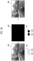
- FIG. 6 A is a schematic drawing for explaining an image viewed by a user using shutter glasses in case that the display system of FIG. 1 operates in a private mode.
- FIG. 6 B is a schematic drawing for explaining an image viewed by a surrounding person who does not use shutter glasses in case that the display system of FIG. 1 operates in a private mode.
- FIG. 7 illustrates a schematic cross-sectional view of another embodiment of a display device of FIG. 1 .
- FIG. 8 illustrates a schematic cross-sectional view of another embodiment of a display device of FIG. 1 .
- FIG. 9 illustrates a schematic cross-sectional view of another embodiment of a display device of FIG. 1 .
- FIG. 10 illustrates a schematic cross-sectional view of another embodiment of a display device of FIG. 1 .
- Spatially relative terms such as “beneath,” “below,” “under,” “lower,” “above,” “upper,” “over,” “higher,” “side” (e.g., as in “sidewall”), and the like, may be used herein for descriptive purposes, and, thereby, to describe one elements relationship to another element(s) as illustrated in the drawings.
- Spatially relative terms are intended to encompass different orientations of an apparatus in use, operation, and/or manufacture in addition to the orientation depicted in the drawings. For example, if the apparatus in the drawings is turned over, elements described as “below” or “beneath” other elements or features would then be oriented “above” the other elements or features.
- the exemplary term “below” can encompass both an orientation of above and below.
- the apparatus may be otherwise oriented (e.g., rotated 90 degrees or at other orientations), and, as such, the spatially relative descriptors used herein interpreted accordingly.
- an element such as a layer
- it may be directly on, connected to, or coupled to the other element or layer or intervening elements or layers may be present.
- an element or layer is referred to as being “directly on,” “directly connected to,” or “directly coupled to” another element or layer, there are no intervening elements or layers present.
- the term “connected” may refer to physical, electrical, and/or fluid connection, with or without intervening elements.
- first, second, and the like are used to describe various constituent elements, these constituent elements are not limited by these terms. These terms are used to distinguish one constituent element from another constituent element. Therefore, first constituent elements described below may be second constituent elements within a technical spirit of the disclosure.
- the components may be connected to each other as separate elements, or the components may be integral with each other.
- Each of the features of the various embodiments of the disclosure may be coupled or combined with each other partly or entirely, and may be technically variously interlocked and driven in a manner that is sufficiently understandable to those skilled in the art.
- Each embodiment may be practicable independently of each other, and may be practicable with together in an interrelationship.
- FIG. 1 illustrates a schematic block diagram of a display system according to an embodiment of the disclosure.
- FIG. 2 is a schematic drawing for explaining a pixel according to an embodiment of the disclosure.
- a display system 1 may include a display device 100 , a private image signal generator 200 , and shutter glasses 300 .
- the display device 100 may be a rigid display or a flexible display.
- the display device 100 may be a portable electronic device, such as a mobile phone, a tablet PC, a laptop computer, a game device, and the like.
- the disclosure is not limited to a specific type of the display device 100 .
- the display device 100 may be used in a large electronic device such as a television, and a small or medium electronic device such as a car navigation device, a smart watch, or a camera.
- the display device 100 may include a display panel 110 displaying an image, a data driver 120 and a scan driver 130 which are driving the display panel 110 , and a timing controller 140 controlling the data driver 120 and the scan driver 130 .
- the private image signal generator 200 may receive image data DATA and a first control signal CONT 1 from an outside.
- the private image signal generator 200 may generate first private image data PV 1 and second private image data PV 2 based on the image data DATA, and may transmit the first private image data PV 1 and the second private image data PV 2 to the timing controller 140 .
- the first control signal CONT 1 may include a general image enable signal for displaying a general image or a private image enable signal for displaying a private image.
- the timing controller 140 may receive the image data DATA, the first private image data PV 1 , the second private image data PV 2 , and a second control signal CONT 2 from the private image signal generator 200 .
- the second control signal CONT 2 may include a panel driving signal for displaying the general image.
- the timing controller 140 may select whether to operate in a general mode or a private mode in response to the panel driving signal.
- the timing controller 140 may output the image data DATA in the general mode, and may output the first private image data PV 1 and the second private image data PV 2 in the private mode.
- the second control signal CONT 2 received by the timing controller 140 may include a main clock signal, a vertical synchronization signal, a horizontal synchronization signal, an image enable signal, and the like in addition to the panel driving signal.
- the timing controller 140 may generate a third control signal CONT 3 for controlling an operation of the scan driver 130 and a fourth control signal CONT 4 for controlling an operation of the data driver 120 based on the second control signal CONT 2 , and may provide the third control signal CONT 3 and the fourth control signal CONT 4 to the scan driver 130 and the data driver 120 , respectively.
- the display panel 110 may include a self-light emitting element.
- the self-light emitting element may include at least one of an organic light emitting diode, a quantum dot light emitting diode, an inorganic material-based micro light emitting diode (for example, a micro LED), and inorganic material-based nano light emitting diodes (for example, a nano LED).
- an organic light emitting diode for example, a quantum dot light emitting diode
- an inorganic material-based micro light emitting diode for example, a micro LED
- inorganic material-based nano light emitting diodes for example, a nano LED.
- the display panel 110 may include a first light emitting area EA 1 , a second light emitting area EA 2 , and a third light emitting area EA 3 (EA 1 , EA 2 , and EA 3 of FIG. 3 ).
- the display panel 110 may include scan lines S 1 to Sn for receiving a gate signal and data lines D 1 to Dm for receiving a data voltage.
- the scan lines S 1 to Sn and the data lines D 1 to Dm may be insulated from each other, and may cross each other.
- FIG. 1 illustrates a pixel PX connected to one of the scan lines S 1 to Sn and one of the data lines D 1 to Dm as an example.
- the configuration of the pixel PX is not limited thereto, and may be modified and implemented.
- a sub-pixel SPX may include a light emitting element LD and a pixel driving circuit PXC for driving the light emitting element LD.
- the light emitting element LD may be a front light emitting diode or a rear light emitting diode.
- the pixel driving circuit PXC may include a first transistor T 1 (or a switching transistor), a second transistor T 2 (or a driving transistor), and a capacitor Cst.
- a first power voltage VDD may be provided to the second transistor T 2
- a second power voltage VSS may be provided to the light emitting element LD.
- the second power voltage VSS may be lower than the first power voltage VDD.
- the first transistor T 1 may output a data signal applied to the data line Dm in response to a scan signal applied to the scan line Sn.
- the capacitor Cst may be charged with a voltage corresponding to the data signal received from the first transistor T 1 .
- the second transistor T 2 may be connected to the light emitting element LD.
- the second transistor T 2 may control a driving current flowing through the light emitting element LD in response to an amount of charge stored in the capacitor Cst.
- the light emitting element LD may emit light during a period in which the second transistor T 2 is turned on.
- the scan driver 130 may be electrically connected to the scan lines S 1 to Sn provided in the display panel 110 to provide a scan signal to the scan lines S 1 to Sn.
- the scan driver 130 may generate a scan signal for driving the scan lines S 1 to Sn based on the third control signal CONT 3 received from the timing controller 140 , and may sequentially output the generated scan signal to the scan lines S 1 to Sn by at least one line part.
- the third control signal CONT 3 may include a scan start pulse, at least one scan shift clock, and the like.
- the scan start pulse may control timing of a first scan signal.
- the at least one scan shift clock may mean one or more clock signals for shifting the scan start pulse.
- the data driver 120 may receive the image data DATA from the timing controller 140 in the general mode.
- the data driver 120 may sample and hold the image data DATA according to the fourth control signal CONT 4 , and may convert the image data DATA into an analog voltage to provide data voltages to the data lines D 1 to Dm.
- the data driver 120 may receive the first private image data PV 1 and the second private image data PV 2 from the timing controller 140 in the private mode.
- the data driver 120 may respectively sample and hold the first private image data PV 1 and the second private image data PV 2 according to the fourth control signal CONT 4 , and may convert the first private image data PV 1 and the second private image data PV 2 into analog voltages to be converted into a first private image data voltage and a second private image data voltage.
- the data driver 120 may provide the first private image data voltage to the data lines D 1 to Dm during a first private frame, and may provide the second private image data voltage to the data lines D 1 to Dm during a second private frame.
- the first private image data voltage and the second private image data voltage may be alternately outputted in parts of a frame (for example, one frame).
- the first private image data voltage may be outputted in the first private frame
- the second private image data voltage may be outputted in the second private frame.
- the fourth control signal CONT 4 may include an output data enable signal and a horizontal start signal, but is not limited thereto.
- the shutter glasses 300 may include a left eye shutter (not shown) and a right eye shutter (not shown).
- the shutter glasses 300 may receive a private synchronization signal PV_Sync, and may open both the left eye shutter and the right eye shutter during the first private frame in response to the private synchronization signal PV_Sync, and may close both the left eye shutter and the right eye shutter during the second private frame.
- the private synchronization signal PV_Sync may be a signal synchronized with the driving timing of the display panel 110 . Accordingly, in case that a user wears the shutter glasses 300 , the user may view the private image displayed on the display panel 110 through the left eye shutter and the right eye shutter thereof.
- FIG. 3 illustrates a schematic cross-sectional view of an embodiment of a display device of FIG. 1 .
- the display device 100 may include a base substrate BL, a backplane structure BP, a pixel layer PXL, a first inorganic insulating layer IOL 1 , a liquid crystal layer LCL, and a second inorganic insulating layer IOL 2 .
- the display device 100 may further include a touch sensor layer TSL on the second inorganic insulating layer IOL 2 .
- the schematic cross-sectional view of FIG. 3 shows a partial configuration of the pixel PX of FIG. 1 .
- the pixel PX may include a first sub-pixel SPX 1 , a second sub-pixel SPX 2 , and a third sub-pixel SPX 3 .
- Configurations in a light emitting layer EML of the first sub-pixel SPX 1 , the second sub-pixel SPX 2 , and the third sub-pixel SPX 3 may be different from each other and the remaining configurations thereof may be substantially a same as each other in FIG. 3 .
- the first sub-pixel SPX 1 will be mainly described and duplicate descriptions will be omitted.
- the first transistor T 1 of the first sub-pixel SPX 1 may include an active pattern ACT 1 , a gate electrode GE 1 , a source electrode 11 , and a drain electrode 12 .
- the base substrate BL may be made of an insulating material such as a resin.
- the base substrate BL may be made of a flexible material to be bendable or foldable, and may have a single-layered structure or a multi-layered structure.
- the base substrate BL may be made of a plastic film such as a polyimide film.
- the backplane structure BP including the pixel driving circuit PXC may be provided on the base substrate BL.
- the backplane structure BP may include a semiconductor layer (e.g., active pattern ACT 1 ), conductive layers (e.g., the gate electrode GE 1 , the source electrode 11 , and the drain electrode 12 ), and insulating layers (e.g., a gate insulating layer GI, a first insulating layer ILL a second insulating layer IL 2 , and a third insulating layer IL 3 ).
- a first buffer layer BF 1 may be formed on the base substrate BL.
- the first buffer layer BF 1 may prevent impurities from being diffused into the transistor T 1 .
- the first buffer layer BF 1 may be omitted depending on a material and process conditions of the base substrate BL.
- the semiconductor layer including the active pattern ACT 1 may be provided on the first buffer layer BF 1 .
- the semiconductor layer may include a poly-silicon semiconductor.
- the semiconductor layer may be formed through a low temperature poly-silicon process (for example, a low temperature poly-silicon (LTPS) process).
- LTPS low temperature poly-silicon
- the gate insulating layer GI may be provided on the semiconductor layer.
- the gate insulating layer GI may be an inorganic insulating layer made of an inorganic material.
- a first conductive layer including the gate electrode GE 1 may be provided on the gate insulating layer GI.
- the gate electrode GE 1 may cover an area corresponding to a channel area of the active pattern ACT 1 .
- the first conductive layer including the gate electrode GE 1 may be made of metal.
- the first conductive layer may be made of at least one of metals such as gold (Au), silver (Ag), aluminum (Al), molybdenum (Mo), chromium (Cr), titanium (Ti), nickel (Ni), neodymium (Nd), and copper (Cu), or an alloy thereof.
- the first conductive layer may be formed as a single layer or a multilayer in which two or more materials of metals and alloys are stacked with each other.
- the first insulating layer IL 1 (or a first interlayer insulating layer) may be provided on the first conductive layer.
- the first insulating layer IL 1 may be an inorganic insulating layer made of an inorganic material.
- the inorganic material a polysiloxane, a silicon nitride, a silicon oxide, or a silicon oxynitride may be used.
- a second conductive layer may be provided on the first insulating layer IL 1 .
- the second conductive layer may be made of at least one of metals such as gold (Au), silver (Ag), aluminum (Al), molybdenum (Mo), chromium (Cr), titanium (Ti), nickel (Ni), neodymium (Nd), and copper (Cu), or an alloy thereof.
- the second conductive layer may be formed as a single layer, but is not limited thereto, and may be formed as a multilayer in which two or more materials among metals and alloys are stacked with each other.
- the second insulating layer IL 2 (or a second interlayer insulating layer) may be provided on the second conductive layer.
- the second insulating layer IL 2 may be an inorganic insulating layer made of an inorganic material.
- the inorganic material a polysiloxane, a silicon nitride, a silicon oxide, or a silicon oxynitride may be used.
- a third conductive layer including the source electrode 11 and the drain electrode 12 may be provided on the second insulating layer IL 2 .
- the source electrode 11 and the drain electrode 12 may contact a source area and a drain area at sides of the active pattern ACT 1 through contact holes formed in the gate insulating layer GI, the first insulating layer ILL and the second insulating layer IL 2 .
- the third conductive layer including the source electrode 11 and the drain electrode 12 may be made of metal.
- the third conductive layer may be made of at least one of metals such as gold (Au), silver (Ag), aluminum (Al), molybdenum (Mo), chromium (Cr), titanium (Ti), nickel (Ni), neodymium (Nd), and copper (Cu), or an alloy thereof.
- a passivation layer may be further provided on the third conductive layer.
- the passivation layer may be an inorganic insulating layer made of an inorganic material.
- the inorganic material a polysiloxane, a silicon nitride, a silicon oxide, or a silicon oxynitride may be used.
- the third insulating layer IL 3 may be provided on the third conductive layer (or the passivation layer).
- the third insulating layer IL 3 may be an organic insulating layer made of an organic material.
- an organic insulating material such as a polyacryl-based compound, a polyimide-based compound, a fluorine-based carbon compound such as Teflon, and a benzocyclobutene compound may be used.
- the third insulating layer IL 3 may be an inorganic insulating layer made of an inorganic material.
- FIG. 3 illustrates that the third insulating layer IL 3 may be provided on the second insulating layer IL 2 , but an insulating layer may be variously disposed.
- the passivation layer may be provided on the source and drain electrodes 11 and 12 , and a first pixel electrode PEL 1 may be provided on the passivation layer.
- the pixel layer PXL may be provided on the backplane structure BP.
- the pixel layer PXL may include a light emitting element LD connected to a pixel circuit (PXC of FIG. 2 ).
- the light emitting element LD may include the first pixel electrode PEL 1 , a hole transport layer HTL, a first light emitting layer EML 1 , an electron transport layer ETL, and a second pixel electrode PEL 2 .
- the first pixel electrode PEL 1 may be made of a metal layer such as silver (Ag), magnesium (Mg), aluminum (Al), platinum (Pt), lead (Pd), gold (Au), nickel (Ni), neodymium (Nd), iridium (Ir), and chromium (Cr), and an alloy thereof and/or an indium tin oxide (ITO), an indium zinc oxide (IZO), a zinc oxide (ZnO), and indium tin zinc oxide (ITZO).
- the first pixel electrode PEL 1 may be connected to the drain electrode 12 through a contact hole.
- a bank layer BK (or a pixel defining film) partitioning a first light emitting area EA 1 , a second light emitting area EA 2 , and a third light emitting area EA 3 may be provided on the third insulating layer IL 3 on which the first pixel electrode PEL 1 is formed.
- the bank layer BK may be an organic insulating layer made of an organic material.
- the organic material may include an acryl resin, an epoxy resin, a phenolic resin, a polyamide resin, a polyimide resin, or the like.
- the bank layer BK may include a light absorbing material, or may serve to absorb light introduced from an outside by a light absorbing agent being applied thereon.
- the bank layer BK may include a carbon-based black pigment.
- the bank layer BK may include an opaque metallic material such as chromium (Cr), molybdenum (Mo), an alloy (MoTi) of molybdenum and titanium, tungsten (W), vanadium (V), niobium (Nb), tantalum (Ta), manganese (Mn), cobalt (Co), or nickel (Ni), or a combination thereof, which has a high light absorption rate.
- the bank layer BK may expose an upper surface of the first pixel electrode PEL 1 , and may protrude from the third insulating layer IL 3 along a circumference of the light emitting area EA (e.g., the first light emitting area EA 1 , the second light emitting area EA 2 , or the third light emitting area EA 3 ).
- the bank layer BK may include openings corresponding to the light emitting area EA.
- the hole transport layer HTL may be provided on the upper surface of the first pixel electrode PEL 1 exposed by the bank layer BK. Through the hole transport layer HTL, holes may move to the light emitting layer EML.
- the light emitting layer EML may be provided on the hole transport layer HTL in the light emitting area EA surrounded by the bank layer BK.
- the light emitting layer EML may be configured as an organic light emitting layer.
- the light emitting layer EML may emit light such as red light, green light, or blue light.
- the first light emitting layer EML 1 of the first sub-pixel SPX 1 may emit red light
- the second light emitting layer EML 2 of the second sub-pixel SPX 2 may emit green light
- the third light emitting layer EML 3 of the third sub-pixel SPX 3 may emit blue light.
- the electron transport layer ETL may be provided on the light emitting layer EML.
- the electron transport layer ETL may be integrally formed. Accordingly, the electron transport layer ETL may contact an upper surface of the bank layer BK.
- the hole transport layer HTL and the electron transport layer ETL may be omitted.
- a functional layer such as a hole injection layer HIL and an electron injection layer EIL may be added.
- the second pixel electrode PEL 2 may be provided on the electron transport layer ETL of the light emitting area EA.
- the second pixel electrode PEL 2 and common electrode CD may be integral with each other.
- a second power voltage VSS may be supplied to the second pixel electrode PEL 2 .
- the second pixel electrode PEL 2 may be made of a metal layer such as silver (Ag), magnesium (Mg), aluminum (Al), platinum (Pt), lead (Pd), gold (Au), nickel (Ni), neodymium (Nd), iridium (Ir), or chromium (Cr), or a combination thereof, and/or a transparent conductive layer such as ITO, IZO, ZnO, or ITZO.
- the common electrode CD may be formed of a multilayer of a double layer or more including a thin metal layer, for example, a triple layer of ITO/Ag/ITO.
- the first inorganic insulating layer IOL 1 may be formed on the common electrode CD including the second pixel electrode PEL 2 .
- the liquid crystal layer LCL may be formed on the first inorganic insulating layer IOL 1 .
- the second inorganic insulating layer IOL 2 may be formed on the liquid crystal layer LCL.
- the first inorganic insulating layer IOL 1 and the second inorganic insulating layer IOL 2 may be formed by including one or more material(s) selected from a silicon nitride, an aluminum nitride, a zirconium nitride, a titanium nitride, a hafnium nitride, a tantalum nitride, a silicon oxide, an aluminum oxide, a titanium oxide, a tin oxide, a cerium oxide, and a silicon oxynitride (SiON).
- the first inorganic insulating layer IOL 1 and the second inorganic insulating layer IOL 2 may be formed by a chemical vapor deposition method.
- the liquid crystal layer LCL may include liquid crystal molecules.
- the liquid crystal layer LCL may be provided in which liquid crystal molecules having dielectric anisotropy are arranged.
- the liquid crystal molecules are not particularly limited as long as they are typically used liquid crystal molecules.
- the liquid crystal molecule may include an alkenyl-based liquid crystal compound, an alkoxy-based liquid crystal compound, or the like.
- the liquid crystal molecule may have a negative dielectric anisotropy or a positive dielectric anisotropy, but is not limited thereto.
- the liquid crystal layer LCL may be a polymer dispersed liquid crystal layer such as a polymer dispersed liquid crystal (PDLC) and a polymer dispersed liquid crystal (PNLC), or a combination thereof.
- the polymer dispersed liquid crystal layer may include disorderly arranged liquid crystals in a polymer matrix. As described above, since the polymer dispersed liquid crystal layer has the liquid crystals arranged disorderly in the polymer matrix, in case that an electric field is not formed, light irradiated from an outside to the polymer dispersed liquid crystal layer may be scattered.
- the liquid crystals disorderly arranged in the polymer matrix included in the polymer dispersed liquid crystal layer may be arranged in a line by the electric field, and because of this, a vibration direction of the light irradiated from the outside to the polymer dispersed liquid crystal layer may be changed.
- a first switch electrode SW 1 may be disposed on the first inorganic insulating layer IOL 1 to overlap the bank layer BK in a thickness direction thereof (or in a plan view).
- a second switch electrode SW 2 may be disposed on the second inorganic insulating layer IOL 2 to overlap the first switch electrode SW 1 in a thickness direction thereof (or in a plan view).
- shapes of the first switch electrode SW 1 and the second switch electrode SW 2 are not limited thereto, the first switch electrode SW 1 may be integrally formed on the entire area of the first inorganic insulating layer IOL 1 , and the second switch electrode SW 2 may be integrally formed on the entire area of the second inorganic insulating layer IOL 2 .
- the first switch electrode SW 1 and the second switch electrode SW 2 may be formed of a transparent conductive layer such as an indium tin oxide (ITO), an indium zinc oxide (IZO), a zinc oxide (ZnO), or an indium tin zinc oxide (ITZO).
- ITO indium tin oxide
- IZO indium zinc oxide
- ZnO zinc oxide
- ITZO indium tin zinc oxide
- the arrangement of liquid crystal molecules in the liquid crystal layer LCL may vary according to an electrical signal applied between the first switch electrode SW 1 and the second switch electrode SW 2 .
- the liquid crystal molecules in a general mode, since an electric field is not formed between the first switch electrode SW 1 and the second switch electrode SW 2 , the liquid crystal molecules have irregular directions, so that light emitted from the light emitting layer EML may be scattered by the liquid crystal molecules. Accordingly, an image displayed on the display device 100 may have a wide viewing angle.
- the liquid crystal molecules in a private mode, since the electric field is formed between the first switch electrode SW 1 and the second switch electrode SW 2 , the liquid crystal molecules have a constant direction, so that a vibration direction of light emitted from the light emitting layer EML may be changed by the liquid crystal molecules. Accordingly, the light emitted from the light emitting layer EML may be outputted on the display device 100 as about 90 degree linearly polarized light. A reason why only a user of the display device 100 may normally view an image displayed on a display panel 110 by using shutter glasses 300 will be described in detail below with reference to FIG. 4 to FIG. 6 B .
- the display device 100 may further include the touch sensor layer TSL on the second inorganic insulating layer IOL 2 .
- a second buffer layer BF 2 may be further included between the second inorganic insulating layer IOL 2 and the touch sensor layer TSL.
- the second buffer layer BF 2 may be formed on the second switch electrode SW 2 and the second inorganic insulating layer IOL 2 .
- the second buffer layer BF 2 may include an inorganic layer or an organic insulating layer.
- the touch sensor layer TSL may include a touch electrode TE, a low refractive index flat layer LRF, and a touch insulating layer TS_IL.
- the touch sensor layer TSL is illustrated as a single-layered structure for acquiring coordinate information by a cell cap method, but the touch sensor layer TSL may include touch insulating layers and touch electrode layers, and may have a double-layered structure for acquiring coordinate information by a mutual cap method.
- the touch electrode TE may have a single-layered structure or a multi-layered structure.
- a conductive layer with the multi-layered structure may include at least two or more of transparent conductive layers and metal layers.
- the multi-layered conductive layer may include metal layers including different metals.
- the transparent conductive layer may include an indium tin oxide (ITO), an indium zinc oxide (IZO), a zinc oxide (ZnO), an indium tin zinc oxide (ITZO), a PEDOT, a metal nano wire, or a graphene.
- the metal layer may include at least one of molybdenum (Mo), silver (Ag), titanium (Ti), copper (Cu), aluminum (Al), and an alloy thereof.
- the touch electrode TE may have a mesh structure including a mesh hole MH and a body portion BD.
- the mesh hole MH may overlap the light emitting area EA in a thickness direction thereof (or in a plan view), and an area of the mesh hole MH may be larger than an area of the light emitting area EA.
- the body portion BD may overlap the bank layer BK (or the pixel defining film) in a thickness direction thereof (or in a plan view), and a width of the body portion BD may be smaller than a width of the bank layer BK.
- the low refractive index flat layer LRF may have a relatively smaller refractive index than the touch insulating layer TS-IL to be described below.
- the low refractive index flat layer LRF may not overlap the light emitting areas EA 1 , EA 2 , and EA 3 , and may overlaps the non-light emitting area, in a plan view.
- the low refractive index flat layer LRF may overlap the bank layer BK (or the pixel defining film) in the thickness direction, in a plan view, and a width of the low refractive index flat layer LRF may be smaller than that of the bank layer BK.
- the low refractive index flat layer LRF may include holes in a plan view.
- the hole of the low refractive index flat layer LRF according to an embodiment may have a circular shape in a plan view, and light (for example, light emitted from the light emitting layer EML) may be evenly emitted from all of edges of the hole.
- the touch insulating layer TS-IL may be disposed on the touch electrode TE, the low refractive index flat layer LRF, and the second buffer layer BF 2 .
- the touch insulating layer TS-IL may include an inorganic or organic material.
- the inorganic material may include at least one of an aluminum oxide, a titanium oxide, a silicon oxide, a silicon oxynitride, a zirconium oxide, and a hafnium oxide.
- the organic material may include at least one of an acryl-based resin, a methacrylic-based resin, a polyisoprene, a vinyl-based resin, an epoxy-based resin, a urethane-based resin, a cellulose-based resin, a siloxane-based resin, a polyimide-based resin, a polyamide-based resin, and a perylene-based resin.
- FIG. 4 is a schematic drawing for explaining the general mode of the display system of FIG. 1 .
- emitted light EL emitted from the light emitting layer EML of the display device 100 does not vibrate in a specific direction but may vibrate in all directions.
- the liquid crystal molecules of the liquid crystal layer LCL may have an irregular directions.
- the emitted light EL may be scattered by the liquid crystal molecules of the liquid crystal layer LCL.
- Light EL 1 outputted from the liquid crystal layer LCL does not vibrate in a specific direction but may vibrate in all directions. Accordingly, a user USR may view an image having a wide viewing angle.
- FIG. 5 A and FIG. 5 B are schematic drawings for explaining the private mode of the display system of FIG. 1 .
- FIG. 6 A is a schematic drawing for explaining an image visible to the user USR using shutter glasses in case that the display system of FIG. 1 operates in the private mode.
- FIG. 6 B is a schematic drawing for explaining an image visible to a surrounding person who does not use shutter glasses in case that the display system of FIG. 1 operates in the private mode.
- the emitted light EL emitted from the light emitting layer EML of the display device 100 does not vibrate in a specific direction but may vibrate in all directions.
- the liquid crystal molecules of the liquid crystal layer LCL may have a constant direction.
- a vibration direction of the emitted light EL may be changed by the liquid crystal molecules of the liquid crystal layer LCL.
- the liquid crystal layer LCL may change the vibration direction of the emitted light EL by about 90 degrees.
- the light EL 1 outputted from the liquid crystal layer LCL may be about 90 degree linearly polarized light.
- the shutter glasses 300 may include a right eye shutter 300 a and a left eye shutter 300 b.
- Each of the right eye shutter 300 a and the left eye shutter 300 b may include a first polarizing plate POL 1 , a liquid crystal layer LCL′, and a second polarizing plate POL 2 .
- the liquid crystal layer LCL′ may be disposed between the first polarizing plate POL 1 and the second polarizing plate POL 2 .
- the first polarizing plate POL 1 and the second polarizing plate POL 2 according to an embodiment may be about 90 degree linear polarizers.
- the light EL 1 outputted from the liquid crystal layer LCL of the display device 100 may be incident on the first polarizer POL 1 .
- the first polarizer POL 1 may transmit a component vibrating in a about 90 degree direction of a phase axis among components of the light EL 1 .
- the shutter glasses 300 may receive a private synchronization signal PV_Sync, and may open both the right eye shutter 300 a and the left eye shutter 300 b during a first private frame in response to the private synchronization signal PV_Sync.
- An opening of the right eye shutter 300 a and the left eye shutter 300 b may mean that the liquid crystal layers LCL′ of the right eye shutter 300 a and the left eye shutter 300 b transmit the about 90 degree linearly polarized light EL 1 as it is without changing the vibration direction thereof.
- the light EL 1 passing through the liquid crystal layers LCL′ of the right eye shutter 300 a and the left eye shutter 300 b may be incident on the second polarizer POL 2 . Since the second polarizer POL 2 transmits a component that vibrates in the about 90 degree direction of the phase axis among light components, the about 90 degree linearly polarized light EL 1 may pass through the second polarizer POL 2 . Light EL 2 may be the about 90 degree linearly polarized light as the light EL 1 . Accordingly, the light EL 2 outputted from the second polarizer POL 2 may be visible to the user USR.
- the shutter glasses 300 may receive a private synchronization signal PV_Sync, and may close both the right eye shutter 300 a and the left eye shutter 300 b during a second private frame in response to the private synchronization signal PV_Sync.
- a closing of the right eye shutter 300 a and the left eye shutter 300 b may mean that the liquid crystal layers LCL′ of the right eye shutter 300 a and the left eye shutter 300 b turn the vibration direction of the about 90 degree linearly polarized light EL 1 by about 90 degrees to be about 180 degree linearly polarized.
- the light EL 1 passing through the liquid crystal layers LCL′ of the right eye shutter 300 a and the left eye shutter 300 b may be incident on the second polarizer POL 2 . Since the second polarizer POL 2 transmits a component that vibrates in the about 90 degree direction of the phase axis among light components, the about 180 degree linearly polarized light EL 1 may not pass through the second polarizer POL 2 . Accordingly, the light EL 1 may not be visible to the user USR.
- the shutter glasses 300 may be for realizing private image display, and the shutter glasses 300 may allow a first private image IMG 1 to be incident on right and left eyes of the user USR through the opening of the right eye shutter 300 a and the left eye shutter 300 b , and may prevent a second private image IMG 2 from being incident on the right and left eyes of the user USR through the closing of the right eye shutter 300 a and the left eye shutter 300 b .
- the first private image IMG 1 may be a normal image to be displayed on the display device 100
- the second private image IMG 2 may be one of a black image, an inverted image of the first private image IMG 1 , and a noise image.
- the user USR since the user USR recognizes the first private image IMG 1 and does not recognize the second private image IMG 2 , the user USR may view the first private image IMG 1 .
- the first private image IMG 1 may correspond to the first private image data PV 1 of FIG. 1
- the second private image IMG 2 may correspond to the second private image data PV 2 of FIG. 1 .
- the first private frame and the second private frame may be alternately provided in units of frames.
- the unit frame may be 1 frame.
- the first private frame in which the first private image IMG 1 is provided and the second private frame in which the second private image IMG 2 is provided may be alternately provided at cycles of about 240 Hz.
- a driving frequency of the display device 100 is about 60 Hz
- the first private frame in which the first private image IMG 1 is provided and the second private frame in which the second private image IMG 2 is provided may be alternately provided at cycles of about 120 Hz.
- FIG. 6 B in case that a surrounding person not wearing the shutter glasses 300 views the display device 100 driven in the private mode, since the surrounding person recognizes both the first private image IMG 1 and the second private image IMG 2 , the surrounding person may view a third private image IMG 3 in which the first private image IMG 1 and the second private image IMG 2 are mixed.
- FIG. 6 B illustrates the second private image IMG 2 as a black image. For this reason, since luminance of the third private image IMG 3 is significantly lower than that of the first private image IMG 1 , the surrounding person not wearing the shutter glasses 300 cannot normally view the first private image IMG 1 outputted from the display device 100 .
- the third private image IMG 3 may be recognized as a white image having significantly higher luminance than the first private image IMG 1 .
- the third private image IMG 3 may be recognized as a noise image.
- FIG. 7 illustrates a schematic cross-sectional view of another embodiment of a display device of FIG. 1 .
- a display device 100 _ 1 illustrated in FIG. 7 may be different from the display device 100 illustrated in FIG. 3 in that the display device 100 _ 1 further includes color filters CF 1 , CF 2 , and CF 3 , and the remaining configurations thereof are substantially a same as those of the display device 100 illustrated in FIG. 3 .
- the display device 100 _ 1 may further include a black matrix BM and color filters CF 1 , CF 2 , and CF 3 on the touch sensor layer TSL.
- the black matrix BM may be provided on the touch insulating layer TS-IL.
- the black matrix BM may absorb or block light introduced from an outside.
- the black matrix BM may include an organic light blocking material.
- the organic light blocking material may include at least one of a carbon black and a titan black, but is not limited thereto.
- the black matrix BM may include openings OP 1 , OP 2 , and OP 3 .
- the black matrix BM may be formed by a patterning process or a printing process using a mask.
- the black matrix BM may be provided to overlap the bank layer BK in a plan view.
- the black matrix BM may be disposed to cover the conductive electrode TE of the touch sensor layer TSL.
- the black matrix BM may be disposed to avoid the light emitting areas EA 1 , EA 2 , and EA 3 .
- the black matrix BM may be provided in a form of a pattern including the first opening OP 1 overlapping the first light emitting area EA 1 , the second opening OP 2 overlapping the second light emitting area EA 2 , and the third opening OP 3 overlapping the third light emitting area EA 3 , in a plan view.
- each of the color filters CF 1 , CF 2 , and CF 3 may be one of a red color filter, a green color filter, and a blue color filter.
- the first color filter CF 1 may be a red color filter
- the second color filter CF 2 may be a green color filter
- the third color filter CF 3 may be a blue color filter.
- the color filters CF 1 , CF 2 , and CF 3 may contact (e.g., directly contact) at least some of upper and side surfaces of the black matrix BM.
- the color filters CF 1 , CF 2 , and CF 3 may be disposed (e.g., directly disposed) on the black matrix BM.
- FIG. 8 illustrates a schematic cross-sectional view of another embodiment of the display device of FIG. 1 .
- a display device 100 _ 2 illustrated in FIG. 8 may be different from the display device 100 _ 1 illustrated in FIG. 7 in that disposition positions of the first switch electrode SW 1 , the second switch electrode SW 2 , and the liquid crystal layer LCL are changed, except for the remaining configuration, but the remaining configurations are substantially a same as each other.
- the liquid crystal layer LCL of the display device 100 _ 1 illustrated in FIG. 7 may be formed between the first inorganic insulating layer IOL 1 and the second inorganic insulating layer IOL 2 .
- the first switch electrode SW 1 may be formed on the first inorganic insulating layer IOL 1 to overlap the bank layer BK in a thickness direction thereof (or in a plan view), and the second switch electrode SW 2 may be formed on the second inorganic insulating layer IOL 2 to face the first switch electrode SW 1 .
- the liquid crystal layer LCL of the display device 100 _ 2 illustrated in FIG. 8 may be formed between the second buffer layer BF 2 and the color filters CF 1 , CF 2 , and CF 3 , and an organic insulating layer OL may be formed between the first inorganic insulating layer IOL 1 and the second inorganic insulating layer IOL 2 .
- the first inorganic insulating layer IOL 1 , the organic insulating layer OL, and the second inorganic insulating layer IOL 2 that are sequentially stacked with each other may function as an encapsulation layer sealing the pixel layer PXL.
- the first inorganic insulating layer IOL 1 and the second inorganic insulating layer IOL 2 may protect the pixel layer PXL from moisture or oxygen, and the organic insulating layer OL may protect the pixel layer PXL from foreign particles such as dust particles.
- the organic insulating layer OL may include an acryl-based organic insulating layer, but is not limited thereto.
- an encapsulation layer may include a first inorganic insulating layer IOL 1 disposed on the pixel layer PXL, an organic insulating layer OL disposed on the first inorganic insulating layer IOL 1 , and a second inorganic insulating layer IOL 2 disposed on the organic insulating layer OL.
- the first switch electrode SW 1 may be formed on the low refractive index flat layer LRF to overlap the body portion BD of the touch electrode TE in a thickness direction thereof (or in a plan view), and the second switch electrode SW 2 may be formed on the liquid crystal layer LCL to face the first switch electrode SW 1 .
- the second switch electrode SW 2 may be covered by the black matrix BM.
- FIG. 9 illustrates a schematic cross-sectional view of another embodiment of the display device of FIG. 1 .
- a display device 100 _ 3 illustrated in FIG. 9 may be different from the display device 100 illustrated in FIG. 3 in which the base substrate (or base layer) BL is a flexible substrate and the second inorganic insulating layer IOL 2 is disposed on a surface of the liquid crystal layer LCL in that a base substrate BL 1 is a rigid substrate and an encapsulation substrate BL 2 is disposed on a surface of the liquid crystal layer LCL, but the remaining components are substantially a same as each other.
- the base substrate BL 1 and the encapsulation substrate BL 2 may be made of a transparent insulating material such as glass and quartz. Accordingly, the encapsulation substrate BL 2 may transmit light emitted from the light emitting layer EML.
- FIG. 10 illustrates a schematic cross-sectional view of another embodiment of the display device of FIG. 1 .
- a display device 100 _ 4 illustrated in FIG. 10 may be different from the display device 10 _ 1 illustrated in FIG. 7 in which the base substrate BL is a flexible substrate and the second inorganic insulating layer IOL 2 is disposed on a surface of the liquid crystal layer LCL in that a base substrate BL 1 is a rigid substrate and an encapsulation substrate BL 2 is disposed on a surface of the liquid crystal layer LCL, but the remaining components are substantially a same as each other.
- the base substrate BL 1 and the encapsulation substrate BL 2 may be made of a transparent insulating material such as glass and quartz. Accordingly, the encapsulation substrate BL 2 may transmit light emitted from the light emitting layer EML.
- the display devices 100 _ 1 , 100 _ 2 , 100 _ 3 , and 100 _ 4 illustrated in FIG. 7 to FIG. 10 may have some configurations different from those of the display device 100 illustrated in FIG. 3 , but may provide substantially a same effect in that they convert the light that is emitted from the light emitting layer EML to vibrate in all directions into about 90 degree linearly polarized light by using the liquid crystal layer LCL in the private mode.
Landscapes
- Physics & Mathematics (AREA)
- Nonlinear Science (AREA)
- Engineering & Computer Science (AREA)
- General Physics & Mathematics (AREA)
- Optics & Photonics (AREA)
- Crystallography & Structural Chemistry (AREA)
- Theoretical Computer Science (AREA)
- Chemical & Material Sciences (AREA)
- General Engineering & Computer Science (AREA)
- Mathematical Physics (AREA)
- Human Computer Interaction (AREA)
- Microelectronics & Electronic Packaging (AREA)
- Ophthalmology & Optometry (AREA)
- Health & Medical Sciences (AREA)
- General Health & Medical Sciences (AREA)
- Electroluminescent Light Sources (AREA)
- Devices For Indicating Variable Information By Combining Individual Elements (AREA)
Abstract
Description
Claims (10)
Applications Claiming Priority (2)
| Application Number | Priority Date | Filing Date | Title |
|---|---|---|---|
| KR10-2022-0030508 | 2022-03-11 | ||
| KR1020220030508A KR20230134037A (en) | 2022-03-11 | 2022-03-11 | Display device and display system |
Publications (2)
| Publication Number | Publication Date |
|---|---|
| US20230288768A1 US20230288768A1 (en) | 2023-09-14 |
| US12204220B2 true US12204220B2 (en) | 2025-01-21 |
Family
ID=87899974
Family Applications (1)
| Application Number | Title | Priority Date | Filing Date |
|---|---|---|---|
| US17/942,250 Active 2042-09-12 US12204220B2 (en) | 2022-03-11 | 2022-09-12 | Display device and display system |
Country Status (3)
| Country | Link |
|---|---|
| US (1) | US12204220B2 (en) |
| KR (1) | KR20230134037A (en) |
| CN (1) | CN116736569A (en) |
Citations (7)
| Publication number | Priority date | Publication date | Assignee | Title |
|---|---|---|---|---|
| KR101562285B1 (en) | 2009-12-28 | 2015-10-21 | 엘지디스플레이 주식회사 | 3 3D images organic electro-luminescence device |
| US20160252785A1 (en) * | 2013-11-11 | 2016-09-01 | Toppan Printing Co., Ltd. | Liquid crystal display device |
| US10297779B1 (en) | 2017-10-30 | 2019-05-21 | Wuhan China Star Optoelectronics Technology Co., Ltd. | OLED display device and process for manufacturing the same |
| KR20210081786A (en) | 2019-12-24 | 2021-07-02 | 엘지디스플레이 주식회사 | Display Device |
| KR102319769B1 (en) | 2012-12-25 | 2021-10-29 | 가부시키가이샤 한도오따이 에네루기 켄큐쇼 | Resistor, display device, and electronic device |
| US20230129697A1 (en) * | 2021-10-22 | 2023-04-27 | Sharp Display Technology Corporation | Liquid crystal panel and display device |
| US20230236448A1 (en) * | 2022-01-21 | 2023-07-27 | Sharp Display Technology Corporation | Liquid crystal display device |
-
2022
- 2022-03-11 KR KR1020220030508A patent/KR20230134037A/en active Pending
- 2022-09-12 US US17/942,250 patent/US12204220B2/en active Active
-
2023
- 2023-01-04 CN CN202310007575.5A patent/CN116736569A/en active Pending
Patent Citations (7)
| Publication number | Priority date | Publication date | Assignee | Title |
|---|---|---|---|---|
| KR101562285B1 (en) | 2009-12-28 | 2015-10-21 | 엘지디스플레이 주식회사 | 3 3D images organic electro-luminescence device |
| KR102319769B1 (en) | 2012-12-25 | 2021-10-29 | 가부시키가이샤 한도오따이 에네루기 켄큐쇼 | Resistor, display device, and electronic device |
| US20160252785A1 (en) * | 2013-11-11 | 2016-09-01 | Toppan Printing Co., Ltd. | Liquid crystal display device |
| US10297779B1 (en) | 2017-10-30 | 2019-05-21 | Wuhan China Star Optoelectronics Technology Co., Ltd. | OLED display device and process for manufacturing the same |
| KR20210081786A (en) | 2019-12-24 | 2021-07-02 | 엘지디스플레이 주식회사 | Display Device |
| US20230129697A1 (en) * | 2021-10-22 | 2023-04-27 | Sharp Display Technology Corporation | Liquid crystal panel and display device |
| US20230236448A1 (en) * | 2022-01-21 | 2023-07-27 | Sharp Display Technology Corporation | Liquid crystal display device |
Non-Patent Citations (2)
| Title |
|---|
| Rui Bao et al., "Photo-polymerization of liquid crystalline monomer in oriented liquid crystal phase", Chinese Chemical Letters, Mar. 1, 2020, pp. 1330-1333, vol. 21, No. 11. |
| US 9,466,619 B2, 10/2016, Yamazaki (withdrawn) |
Also Published As
| Publication number | Publication date |
|---|---|
| CN116736569A (en) | 2023-09-12 |
| KR20230134037A (en) | 2023-09-20 |
| US20230288768A1 (en) | 2023-09-14 |
Similar Documents
| Publication | Publication Date | Title |
|---|---|---|
| US11864407B2 (en) | Display device with structure for preventing organic material overflow | |
| US11217639B2 (en) | Display device | |
| CN108257972B (en) | display device | |
| CN105679791B (en) | Organic light emitting display device and manufacturing method thereof | |
| JP7682249B2 (en) | display device | |
| US11626456B2 (en) | Display device including stepped section substrate with embedded camera | |
| TW202013343A (en) | Organic light emitting diode display device | |
| EP3699729B1 (en) | Display device and touch sensor | |
| KR102449131B1 (en) | organic light emitting display device | |
| CN104885250A (en) | Transparent organic light-emitting display device and manufacturing method thereof | |
| US12204220B2 (en) | Display device and display system | |
| US20230371345A1 (en) | Display panel and method of manufacturing display panel | |
| KR102866884B1 (en) | Display device | |
| US12462754B2 (en) | Sub-pixel, display device including the same, and driving method thereof | |
| US20250204206A1 (en) | Display device and method of manufacturing the same | |
| US20250393370A1 (en) | Anti-reflection layer, display device, and electronic device including the same | |
| US20250228072A1 (en) | Sub-pixel, display panel including the same, and method of fabricating the display panel | |
| US20250107347A1 (en) | Display panel and method for manufacturing the same | |
| US20250359469A1 (en) | Display panel and display system including the same | |
| US20260024501A1 (en) | Display device and electronic device | |
| US20230320150A1 (en) | Display device | |
| KR20250147720A (en) | Display device comprising lens array | |
| KR20250116212A (en) | Display panel and display device having the same |
Legal Events
| Date | Code | Title | Description |
|---|---|---|---|
| AS | Assignment |
Owner name: SAMSUNG DISPLAY CO., LTD., KOREA, REPUBLIC OF Free format text: ASSIGNMENT OF ASSIGNORS INTEREST;ASSIGNOR:OH, EON SEOK;REEL/FRAME:061409/0107 Effective date: 20220817 |
|
| FEPP | Fee payment procedure |
Free format text: ENTITY STATUS SET TO UNDISCOUNTED (ORIGINAL EVENT CODE: BIG.); ENTITY STATUS OF PATENT OWNER: LARGE ENTITY |
|
| STPP | Information on status: patent application and granting procedure in general |
Free format text: DOCKETED NEW CASE - READY FOR EXAMINATION |
|
| STPP | Information on status: patent application and granting procedure in general |
Free format text: NON FINAL ACTION MAILED |
|
| STPP | Information on status: patent application and granting procedure in general |
Free format text: RESPONSE TO NON-FINAL OFFICE ACTION ENTERED AND FORWARDED TO EXAMINER |
|
| STPP | Information on status: patent application and granting procedure in general |
Free format text: NON FINAL ACTION MAILED |
|
| STPP | Information on status: patent application and granting procedure in general |
Free format text: FINAL REJECTION MAILED |
|
| STPP | Information on status: patent application and granting procedure in general |
Free format text: ADVISORY ACTION MAILED |
|
| STPP | Information on status: patent application and granting procedure in general |
Free format text: DOCKETED NEW CASE - READY FOR EXAMINATION |
|
| STPP | Information on status: patent application and granting procedure in general |
Free format text: NON FINAL ACTION MAILED |
|
| STPP | Information on status: patent application and granting procedure in general |
Free format text: RESPONSE TO NON-FINAL OFFICE ACTION ENTERED AND FORWARDED TO EXAMINER |
|
| STPP | Information on status: patent application and granting procedure in general |
Free format text: NOTICE OF ALLOWANCE MAILED -- APPLICATION RECEIVED IN OFFICE OF PUBLICATIONS |
|
| ZAAB | Notice of allowance mailed |
Free format text: ORIGINAL CODE: MN/=. |
|
| STPP | Information on status: patent application and granting procedure in general |
Free format text: PUBLICATIONS -- ISSUE FEE PAYMENT VERIFIED |
|
| STCF | Information on status: patent grant |
Free format text: PATENTED CASE |