US12200367B2 - Ambient light sensing - Google Patents
Ambient light sensing Download PDFInfo
- Publication number
- US12200367B2 US12200367B2 US17/827,645 US202217827645A US12200367B2 US 12200367 B2 US12200367 B2 US 12200367B2 US 202217827645 A US202217827645 A US 202217827645A US 12200367 B2 US12200367 B2 US 12200367B2
- Authority
- US
- United States
- Prior art keywords
- light
- light sensor
- processor
- camera
- light signal
- Prior art date
- Legal status (The legal status is an assumption and is not a legal conclusion. Google has not performed a legal analysis and makes no representation as to the accuracy of the status listed.)
- Active, expires
Links
- 238000005286 illumination Methods 0.000 claims abstract description 33
- 230000004044 response Effects 0.000 claims 4
- 230000003287 optical effect Effects 0.000 description 58
- 239000004065 semiconductor Substances 0.000 description 11
- 238000000034 method Methods 0.000 description 9
- 238000010586 diagram Methods 0.000 description 6
- 230000006870 function Effects 0.000 description 5
- 238000004519 manufacturing process Methods 0.000 description 5
- 238000001228 spectrum Methods 0.000 description 4
- 239000000758 substrate Substances 0.000 description 3
- 238000012935 Averaging Methods 0.000 description 2
- 230000008859 change Effects 0.000 description 2
- 238000004891 communication Methods 0.000 description 2
- 238000004806 packaging method and process Methods 0.000 description 2
- 238000013519 translation Methods 0.000 description 2
- 230000009471 action Effects 0.000 description 1
- 230000003213 activating effect Effects 0.000 description 1
- 239000003990 capacitor Substances 0.000 description 1
- 230000006835 compression Effects 0.000 description 1
- 238000007906 compression Methods 0.000 description 1
- 238000010276 construction Methods 0.000 description 1
- 230000007246 mechanism Effects 0.000 description 1
- 239000002184 metal Substances 0.000 description 1
- 238000012986 modification Methods 0.000 description 1
- 230000004048 modification Effects 0.000 description 1
- 230000008569 process Effects 0.000 description 1
- 230000003068 static effect Effects 0.000 description 1
- 238000012546 transfer Methods 0.000 description 1
Images


Classifications
-
- H—ELECTRICITY
- H04—ELECTRIC COMMUNICATION TECHNIQUE
- H04N—PICTORIAL COMMUNICATION, e.g. TELEVISION
- H04N23/00—Cameras or camera modules comprising electronic image sensors; Control thereof
- H04N23/70—Circuitry for compensating brightness variation in the scene
- H04N23/71—Circuitry for evaluating the brightness variation
-
- G—PHYSICS
- G01—MEASURING; TESTING
- G01J—MEASUREMENT OF INTENSITY, VELOCITY, SPECTRAL CONTENT, POLARISATION, PHASE OR PULSE CHARACTERISTICS OF INFRARED, VISIBLE OR ULTRAVIOLET LIGHT; COLORIMETRY; RADIATION PYROMETRY
- G01J1/00—Photometry, e.g. photographic exposure meter
- G01J1/42—Photometry, e.g. photographic exposure meter using electric radiation detectors
- G01J1/4204—Photometry, e.g. photographic exposure meter using electric radiation detectors with determination of ambient light
-
- H—ELECTRICITY
- H04—ELECTRIC COMMUNICATION TECHNIQUE
- H04N—PICTORIAL COMMUNICATION, e.g. TELEVISION
- H04N23/00—Cameras or camera modules comprising electronic image sensors; Control thereof
- H04N23/10—Cameras or camera modules comprising electronic image sensors; Control thereof for generating image signals from different wavelengths
- H04N23/11—Cameras or camera modules comprising electronic image sensors; Control thereof for generating image signals from different wavelengths for generating image signals from visible and infrared light wavelengths
-
- H—ELECTRICITY
- H04—ELECTRIC COMMUNICATION TECHNIQUE
- H04N—PICTORIAL COMMUNICATION, e.g. TELEVISION
- H04N23/00—Cameras or camera modules comprising electronic image sensors; Control thereof
- H04N23/50—Constructional details
- H04N23/55—Optical parts specially adapted for electronic image sensors; Mounting thereof
-
- H—ELECTRICITY
- H04—ELECTRIC COMMUNICATION TECHNIQUE
- H04N—PICTORIAL COMMUNICATION, e.g. TELEVISION
- H04N23/00—Cameras or camera modules comprising electronic image sensors; Control thereof
- H04N23/56—Cameras or camera modules comprising electronic image sensors; Control thereof provided with illuminating means
-
- H—ELECTRICITY
- H04—ELECTRIC COMMUNICATION TECHNIQUE
- H04N—PICTORIAL COMMUNICATION, e.g. TELEVISION
- H04N23/00—Cameras or camera modules comprising electronic image sensors; Control thereof
- H04N23/70—Circuitry for compensating brightness variation in the scene
- H04N23/72—Combination of two or more compensation controls
-
- H—ELECTRICITY
- H04—ELECTRIC COMMUNICATION TECHNIQUE
- H04N—PICTORIAL COMMUNICATION, e.g. TELEVISION
- H04N23/00—Cameras or camera modules comprising electronic image sensors; Control thereof
- H04N23/70—Circuitry for compensating brightness variation in the scene
- H04N23/74—Circuitry for compensating brightness variation in the scene by influencing the scene brightness using illuminating means
Definitions
- a camera may be integrated into a video doorbell housing for a door to a home.
- the doorbell camera provides live images to an Internet-connected device (e.g., a mobile phone, tablet device, etc.).
- the image sensor of the camera may be capable of detecting electromagnetic signals in the visible part of the spectrum (e.g., having wavelengths of approximately 400 nm to 700 nm) as well as in the near infra-red (NIR) part of the spectrum (e.g., having wavelengths of approximately 780 nm to 1000 nm).
- NIR near infra-red
- the utility of such cameras in low ambient (e.g., visible light) conditions is facilitated by activating MR light emitting diodes (LEDs).
- one camera is used for visible light (day time) and another camera is used for MR (low ambient light conditions).
- a camera system includes a camera having a camera output, an illumination source having an input, a first light sensor having a first light sensor output, and a second light sensor having a second light sensor output.
- a processor has inputs coupled to the camera output, the first light sensor output, and the second light sensor output, and the processor has an output coupled to the input of the illumination source.
- the processor is configured to receive a first light signal from the first light sensor output, receive a second light signal from the second light sensor output, determine a first weight for the first light signal and a second weight for the second light signal based on a difference between the first and second light signals, calculate a weighted average of the first and second light signals using the first and second weights, and determine whether to turn on the illumination source based on the weighted average.
- an ambient light sensing system in another embodiment, includes a light sensor having a light sensor output, a moveable optical element, and a motor mechanically coupled to the movable optical element.
- the motor has a motor control input.
- a processor is included and has an input coupled to the light sensor output and has a control output coupled to the motor control input.
- the processor is configured to provide a control signal to the motor to actuate the motor to move the movable optical element between a first position and a second position. In the first position light is received by the light sensor after passing through the moveable optical element and a first light sensor signal is received by the processor. In the second position, light is received by the light sensor without passing through the movable optical element and a second light sensor signal is received by the processor.
- the processor is configured to determine an ambient light level based on first light sensor signal and the second light sensor signal.
- an ambient light sensing system in yet another embodiment, includes a light sensor having a light sensor output and a reflective optical element configurable to reflect light from an angle into the light sensor.
- the reflective optical element has a control input.
- a processor has an input coupled to the light sensor output and has a control output.
- the processor is configured to provide a control signal to the control input of the reflective optical element to change the angle of light reflected off of the reflective optical element to the light sensor from a first angle to a second angle.
- the processor is configured to receive a first light signal form the light sensor output corresponding to the first angle and a second light sensor signal from the light sensor output corresponding to the second angle.
- the processor is configured to determine an ambient light level based on first light sensor signal and the second light sensor signal.
- the camera system may be utilized in a doorbell, a security camera, a drone, a cell phone, an industrial system or any other camera system that is capable of operating in low-light, bright-light and other conditions.
- FIG. 1 is a block diagram of a camera system including multiple ambient light sensors, in accordance with an embodiment.
- FIG. 2 is a flowchart illustrating a method of operation of the camera system of FIG. 1 , in accordance with an embodiment.
- FIG. 3 is a flowchart illustrating the determination of weights for computing a weighted average of the signals from the multiple light sensors, in accordance with an embodiment.
- FIGS. 4 and 5 are block diagrams of another embodiment of a camera system in which a motor can move a moveable optical element, in accordance with an example.
- FIG. 6 is a depiction of an actuator mechanically coupled to an optical element, in accordance an embodiment.
- FIG. 7 is another depiction of an actuator mechanically coupled to an optical element, in accordance an embodiment.
- FIG. 8 is a flowchart illustrating a method of operation of the camera system of FIG. 4 , in accordance with an embodiment.
- FIG. 9 is a block diagram of another embodiment of a camera system including a reflective optical element, in accordance with an example.
- FIG. 10 is an array of reflective mirrors of a digital micromirror device, in accordance with an example.
- FIG. 11 is a perspective view of a single reflective mirror of a digital micromirror device, in accordance with an example.
- the NIR camera will produce an enhanced image if NIR lights, e.g., NIR light emitting diodes (NIR LEDs), are illuminated at night.
- NIR light emitting diodes NIR LEDs
- An ambient light sensor may be provided by which the camera system can differentiate a high ambient light condition (e.g., daytime) from a low ambient light condition (e.g., nighttime).
- the ambient light sensor has a “field-of-view” (FOV) in which the sensor receives light from a particular direction and in accordance with a particular angular cone.
- FOV field-of-view
- the ambient light sensor produces a signal indicative of a low ambient light condition so as to cause the camera system to turn ON the NIR LEDs.
- an artificial light source e.g., a lamp, a streetlight, etc.
- the signal from the ambient light sensor will be larger than if the artificial light source was not present.
- the artificial light source may be bright enough to confuse the camera system into determining that the ambient light condition is consistent with daytime (sunny) conditions, but such an artificial light source may be insufficient to adequately illuminate the area around the camera.
- visible light from the headlight of an automobile or a streetlamp may be bright enough to confuse the system into determining that it is daytime, but not bright enough to adequately illuminate the front porch where the video doorbell system containing the camera is located.
- the camera system includes a first ambient light sensor and a second ambient light sensor.
- the FOV of the ambient light sensors are different—one ambient light sensor receives light from one direction, and the other ambient light sensor receives light from a different direction.
- the light signals from the first and second ambient light sensors are averaged together to produce an average ambient light sensor signal. Because the ambient light sensors point in two different directions, even if an artificial light source is in the FOV of one the sensors, the artificial light source is not likely to be in the FOV of the other sensor.
- the average ambient light sensor signal provides a more accurate representation of the ambient light condition of the camera system.
- a second embodiment includes an ambient light sensor, a moveable optical element, and a motor mechanically coupled to the movable optical element.
- the moveable optical element may diffract the light passing through it, so that the light that exits the moveable optical element is at an angle to the light that is received into the moveable optical element.
- the motor is controlled by a processor to move the moveable optical element in front of the light sensor and away from the light sensor. When, the moveable optical element is in front of the light sensor, light received by the ambient light sensor from the optical element is at an angle from the light received by the light sensor when the moveable optical element is moved out of the field-of-view of the ambient light sensor.
- the ambient light sensor is able to receive light from two different directions, and the camera system performs an averaging of the two light signals to provide a more accurate representation of the ambient lighting condition.
- a solenoid could be used to perform linear actuation of the optical element.
- a third embodiment includes a reflective optical (e.g., digital micromirror device) whose reflective surface can be tilted between two different angles to cause light to be received into the ambient light sensor from two different angles.
- the camera system performs an averaging of the two light signals to provide a more accurate representation of the ambient lighting condition.
- FIG. 1 is a block diagram of a camera system 100 in accordance with an embodiment.
- camera system 100 as well as the other camera systems described herein, is implemented as part of video doorbell system (e.g., FIG. 1 may illustrate a printed circuit board (PCB) or semiconductor device which forms part of the camera system—the PCB and/or semiconductor device may be packaged such that camera 108 , illumination source 110 and sensors S 1 and S 2 are not blocked by the packaging but the other components are covered by the packaging).
- Camera system 100 includes a processor 102 , a memory device 104 , a camera 108 , an illumination source 110 , and ambient light sensors S 1 and S 2 .
- the memory device 104 is a non-transitory, storage device such as volatile memory (e.g., random-access memory) or non-volatile storage (e.g., read-only memory).
- Memory device 104 includes software 106 .
- Software 106 is executable by processor 102 .
- Functionality described herein as attributed to the processor 102 is implemented by the processor 102 executing software 106 .
- Processor 102 may include a microprocessor, microcomputer, digital circuitry, analog circuitry, registers and/or a combination thereof.
- Ambient light sensor S 1 is sensitive to light received in its field-of-view (FOV 1 ), and ambient light sensor S 2 is sensitive to light received in its field-of-view (FOV 2 ).
- the ambient light sensors S 1 and S 2 are identical and thus have the same FOV, but ambient light sensor S 1 is mounted in the camera system 100 such that its FOV 1 is pointed in a different direction than the FOV 2 of ambient light sensor S 2 .
- An axis defining each FOV is shown for the sensors.
- Axis S 1 a is generally the mid-point within the cone of FOV 1
- axis S 2 a is the mid-point within the cone of FOV 2 .
- camera system 100 may include more than two light sensors. One or more of the light sensors may be located on the face of the camera system (such as facing in the same direction as the camera), while others may be placed on the side, top or bottom of the camera system 100 .
- the camera 108 (which has its own field of view, FOV 3 ) is any suitable type of image sensor to produce still images or video. This image/video data may be provided to the processor 102 .
- the camera 108 includes both ambient visible light and ambient IR light image capabilities.
- the illumination source 110 includes one or more NIR lights such as NIR LEDs, or any other illumination source capable of providing adequate lighting conditions in low visible light ambient conditions.
- the processor 102 can control the illumination source 110 to be on or off.
- the processor 102 processes light signals (electrical signals that indicate the brightness level of the ambient light received by the sensors) to turn on the illumination source 110 during low ambient light conditions and to turn off the illumination source 110 during bright ambient light conditions.
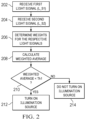
- FIG. 2 is a flow chart illustrating a method of operating the camera system 100 ( FIG. 1 ). The steps of the illustrative method may be performed by the processor 102 upon its execution of software 106 .
- the method includes the processor receiving a first light signal from ambient light sensor S 1 .
- the first light signal is designated L_S 1 .
- the processor also receives a second light signal (L_S 2 ) from ambient light sensor S 2 .
- the order of steps 202 and 204 can be reversed from that shown in FIG. 2 —the processor 102 receiving light signal L_S 2 and then receiving light signal L_S 1 .
- the processor 102 may receive both light signals L_S 1 and L_S 2 concurrently, rather than sequentially.
- both light signals L_S 1 and L_S 2 should be at magnitudes consistent with low lighting conditions (e.g., small amplitude signals).
- an artificial light source is in the FOV of one of the light sensors, then the light signal from that sensor will be substantially larger than the light signal from the other light signal.
- the light signal from sensor S 1 will be larger than the light signal from sensor S 2 , L_S 1 will be greater than L_S 2 .
- the processor 102 computes an average of light signals L_S 1 and L_S 2 to produce an average light signal that may more accurately reflect the actual ambient lighting conditions than just the light signal from one of the light sensors.
- the processor 102 may compute a weighted average of light signals L_S 1 and L_S 2 .
- the processor 102 determines a weight for the light signal L_S 1 and a separate weight for the light signal L_S 2 .
- the weight for the larger of the two light signals is set by the processor 102 to be smaller, and the weight for the smaller of the two light signals is set to be larger.
- FIG. 3 is a flowchart illustrating an example method for setting the weights, and will be described below.
- the processor 102 calculates the weighted average of the light signals L_S 1 and L_S 2 (using their assigned weighting factors). The weighted average is then compared at step 210 to a threshold, Th 1 .
- the threshold Th 1 is a value (e.g., either set during fabrication of the camera system, set based on system specifications, set during system operation by an end-user and/or set during operation by the system) that differentiates daytime lighting conditions form nighttime lighting conditions. If the weighted average is less than the threshold Th 1 (which would be consistent with nighttime lighting conditions), the processor 102 asserts a control signal to turn on illumination source 110 .
- the processor 102 does not cause the illumination source 110 to turn on, or if the illumination source 110 is already on, the processor turns it off.
- the weighted average being equal to Th 1 may result in either the processor turning on the illumination source 110 or turning it off.
- FIG. 3 is a flowchart illustrating an example implementation of step 206 (determination of the weights to be used in the weighted average) from FIG. 2 .
- the weights are determined based on the relative magnitudes of light signals L_S 1 and L_S 2 .
- the processor computes [(L_S 1 ) ⁇ (L_S 2 )] and compares that difference to a second threshold, Th 2 . If L_S 1 is more than threshold Th 2 larger than L_S 2 , then, at step 304 , the processor sets the weight for light signal L_S 2 to be larger than the weight for light signal L_S 1 .
- the processor 102 selects either a preset larger value or a preset smaller value.
- the values for a given weight may be 0.25 or 0.75 (or any smaller or larger fractional or integer value).
- the processor 102 may set the weight for light signal L_S 2 to be 0.75 and the weight for light signal L_S 1 to be 0.25.
- the processor 102 computes the computes (L_S 2 ⁇ L_S 1 ) and compares that difference to the same threshold, Th 2 . If L_S 2 is more than threshold Th 2 larger than L_S 1 , then, at step 308 , the processor sets the weight for light signal L_S 1 to be larger than the weight for light signal L_S 2 . For example, the processor 102 may set the weight for light signal L_S 1 to be 0.75 and the weight for light signal L_S 2 to be 0.25.
- FIG. 4 is a block diagram of a camera system 400 in accordance with another embodiment.
- Camera system 400 includes a processor 402 , a memory device 404 , a camera 408 , an illumination source 410 , a moveable optical element 412 , a motor 414 , and an ambient light sensor S 1 .
- FIG. 4 that are identified with a reference number that has the same last two digits as a feature in FIG. 1 (e.g., processor 102 and processor 402 ) may be implemented in the same (or similar) manner and/or may have the same (or similar) functionality.
- the memory device 404 is a non-transitory, storage device such as volatile memory (e.g., random-access memory) or non-volatile storage (e.g., read-only memory).
- Memory device 404 includes software 406 .
- Software 406 is executable by processor 402 . Functionality described herein as attributed to the processor 402 is implemented by the processor 402 executing software 406 .
- the ambient light sensor S 1 , camera 408 and illumination source 410 may be implemented as described above for camera 108 and illumination source 110 .
- Processor 402 may include a microprocessor, microcomputer, digital circuitry, analog circuitry, registers and/or a combination thereof.
- the moveable optical element 412 may be a film having a prismatic surface, which refracts light as light passes through the film. Accordingly, light entering the film at an incident angle exits the film at a different angle.
- An example of such a film is the Direction Turning Film by Luminit.
- Another example of the optical element 412 is a prism, which also refracts light.
- FIG. 4 illustrates the field-of-view of optical element 412 with a mid-point axis 421 . Due to the refractive property of the optical element 412 , the light exits the optical element along axis 422 into ambient light sensor S 1 .
- the moveable optical element 412 is mechanically coupled to motor 414 .
- the processor 402 generates a control signal 413 and provides the control signal 413 to the motor 414 to operate the motor 414 to move the moveable optical element 412 between a first position and a second position.
- the first position is as shown in FIG. 4 in which light is received by the ambient light sensor S 1 after the light has been refracted by the optical element.
- the second position is as shown in FIG. 5 in which the motor 414 has moved the moveable optical element 412 out of the way of the ambient light sensor S 1 so that light received by the ambient light sensor does not first pass through the moveable optical element.
- the mid-point axis S 1 a of the FOV 1 of the ambient light sensor S 1 is at a different angle that axis 421 of FIG. 4 . Accordingly, one ambient light sensor can be used to sequentially receive light from two different angles.
- the motor 414 may be a stepper motor or other suitable type of mechanism that can be controlled by processor 402 to permit the ambient light sensor S 1 to provide two time-sequenced light signals to the processor that are generated based on light at two different angles.
- a linear actuator may be used in place of a motor to linearly move the moveable optical element.
- FIGS. 6 and 7 illustrates example implementations of how a linear actuator can be coupled to the moveable optical element.
- a linear actuator has an extension rod 626 within a tube 614 along axis 601 .
- the linear actuator forces the extension rod 626 to the right, the extension rod pushes against a tab 635 coupled to (or part of) a turntable 636 .
- the moveable optical element 412 is mounted on the turntable 636 and rotates as the linear actuator forces the extension rod 626 to the right.
- a compression spring 642 provides right to left force against the tab when the linear actuator retracts the extension rod back to the left.
- the moveable optical element 412 may be a prism and rotation in one direction or another may cause light from different angles to pass through the prism to the sensor.
- the spring 636 may be an extension spring.
- FIG. 7 shows an embodiment in which the extension rod is pivotally coupled to one end of a bracket 742 , with the other end of the bracket pivotally coupled to a turntable 736 containing the moveable optical element 412 .
- Rightward translation of the extension rod 626 by the linear actuator causes the turntable 736 (and thus the moveable optical element) to turn counterclockwise.
- Leftward translation of the extension rod 626 causes the turntable 736 (and thus the moveable optical element) to turn clockwise.
- FIG. 8 is a flowchart chart illustrating a method for operating camera system 400 of FIG. 4 .
- the steps 802 - 808 shown in FIG. 8 may be performed by the processor 402 upon its execution of software 406 .
- the processor receives a first light signal from the ambient light sensor S 1 in which the sensor receives light through the moveable optical element 412 located in a first position.
- the first position of step 802 may be the position shown in FIG. 4 in which light refracts through the moveable optical element 412 into the light sensor S 1 .
- the method includes the processor 402 actuating the motor 414 through control signal 413 to cause the motor to move the moveable optical element 412 to a second position in which light through received by the ambient light sensor S 1 does not pass through optical element 412 .
- the processor 402 receives a second light signal from the ambient light sensor S 1 without light having passed through the moveable optical element 412 .
- the moveable optical element 412 in the first position the moveable optical element 412 may not be in front of the ambient light sensor (light received by the sensor is not refracted by the optical element), and in the second position, the moveable optical element 412 is in front of the ambient light sensor (light received by the sensor is refracted by the optical element).
- the processor 402 determines the ambient light level based on the first and second light signals received at steps 802 and 806 .
- the processor 402 may average the two light signals together, and the average may be a weighted average as described above.
- FIG. 9 is a block diagram of a camera system 900 in accordance with another embodiment.
- Camera system 900 includes a processor 902 , a memory device 904 , a camera 908 , an illumination source 910 , a reflective optical element 912 , and an ambient light sensor S 1 .
- FIG. 9 that are identified with a reference number that has the same last two digits as a feature in FIG. 1 and/or a feature in FIG. 4 (e.g., processor 102 , processor 402 and processor 902 ) may be implemented in the same (or similar) manner and/or may have the same (or similar) functionality.
- the camera system 900 of FIG. 9 may have only a single ambient light sensor S 1 .
- the memory device 904 is a non-transitory, storage device such as volatile memory (e.g., random-access memory) or non-volatile storage (e.g., read-only memory).
- Memory device 904 includes software 906 .
- Software 906 is executable by processor 902 .
- Functionality described herein as attributed to the processor 902 is implemented by the processor 902 executing software 906 .
- the ambient light sensor S 1 , camera 908 and illumination source 910 may be implemented as described above for camera 908 and illumination source 910 .
- Processor 902 may include a microprocessor, microcomputer, digital circuitry, analog circuitry, registers and/or a combination thereof.
- the reflective optical element 912 includes a digital micromirror device (DMD).
- DMD digital micromirror device
- a DMD has an optically reflective surface that can be tilted between different angles based on the polarity of a voltage applied to contacts of the DMD.
- FIG. 9 illustrates the reflective surface of the reflective optical element 912 tilted at two different angles (while an actual DMD semiconductor die does not tilt, the individual mirrors formed over the semiconductor die may tilt in one or more directions).
- light along incident axis 921 reflects off of the surface into the ambient light sensor S 1 .
- light along incident axis 922 reflects off of the surface into the ambient light sensor. Accordingly, light from two different angles can be received by the ambient light sensor.
- the processor 902 asserts a control signal 913 to the reflective optical element 912 to change the tilt angle of its reflective surface.
- FIG. 10 shows a top-down view of a DMD 1012 , which can be used to implement reflective optical element 912 .
- the DMD 1012 includes an array of individual mirrors 920 , each of which can be individually controlled by processor 902 to be tilted between two different angles.
- FIG. 11 illustrates a single DMD pixel element 1100 (e.g., individual mirror 920 ). An array of such pixel elements may be formed on a common semiconductor die.
- the DMD pixel element 1100 of the example of FIG. 11 includes a hinge 1116 , an address portion, and a micromirror 1114 .
- the hinge 1116 may be a torsion hinge and may be supported on each side by hinge posts.
- Six bias vias 1108 support spring tips 1126 (two of which are shown in FIG. 11 and two more are present but hidden in this view) and hinge 1116 above the lower layer (also referenced as a “substrate”) 1130 .
- the bias vias 1108 may also operate to relay a bias voltage to hinge 1116 .
- the micromirror 1104 may include a reflective metal surface.
- the micromirror 1104 is supported above the hinge 1116 by a mirror via 1102 .
- the mirror via 1102 may conductively transfer the bias voltage to the micromirror 1104 .
- the bias voltage may be conductively transferred to the spring tips 1126 and hinge 1116 through the six bias vias 1108 .
- the bias voltage may be further transferred from the hinge 1116 to the micromirror 1104 through the mirror via 1102 .
- the address portion of the DMD pixel element 1100 includes two address pads 1112 a , 1112 b that each connect to raised address electrodes 1114 a , 1114 b , respectively.
- address vias 1113 support the raised address electrodes 1114 a , 114 b above each address pad 1112 a , 112 b .
- the address vias 1113 relay a control or address voltage from the address pads 1112 a , 1112 b to the raised address electrodes 1114 a , 114 b .
- the address pads 1112 a , 1112 b may be in communication with control circuitry, such as a static random access memory (SRAM) cell or the like, which selectively applies a control or address voltage to one of the two address pads 1112 a , 112 b to create an electrostatic force between the micromirror 1104 and the raised address electrodes 1114 a , 1114 b .
- control circuitry such as a static random access memory (SRAM) cell or the like, which selectively applies a control or address voltage to one of the two address pads 1112 a , 112 b to create an electrostatic force between the micromirror 1104 and the raised address electrodes 1114 a , 1114 b .
- SRAM static random access memory
- the range of motion of the micromirror 1104 may be limited by spring tips 1126 .
- spring tips 1126 provide a landing point for micromirror 1104 .
- the spring tips 1126 positioned proximate these address elements operate as a landing point for micromirror 1104 .
- the spring tips 1126 on the opposite side and hidden in the view of FIG.
- micromirror 1104 may be tilted in the positive or negative direction until the micromirror 1104 contacts one or more spring tips 1126 .
- the base of the various vias 1102 , 1108 , and 1113 may be referred to as substrate.
- the term “couple” may cover connections, communications, or signal paths that enable a functional relationship consistent with this description. For example, if device A generates a signal to control device B to perform an action: (a) in a first example, device A is coupled to device B by direct connection; or (b) in a second example, device A is coupled to device B through intervening component C if intervening component C does not alter the functional relationship between device A and device B, such that device B is controlled by device A via the control signal generated by device A.
- a device that is “configured to” perform a task or function may be configured (e.g., programmed and/or hardwired) at a time of manufacturing by a manufacturer to perform the function and/or may be configurable (or reconfigurable) by a user after manufacturing to perform the function and/or other additional or alternative functions.
- the configuring may be through firmware and/or software programming of the device, through a construction and/or layout of hardware components and interconnections of the device, or a combination thereof.
- terminal As used herein, the terms “terminal”, “node”, “interconnection”, “pin” and “lead” are used interchangeably. Unless specifically stated to the contrary, these terms are generally used to mean an interconnection between or a terminus of a device element, a circuit element, an integrated circuit, a device or other electronics or semiconductor component.
- the term “light” includes any spectrum of electromagnetic energy including “visible light”, infrared energy, ultraviolet and/or other portions of the electromagnetic emissions spectrum.
- a circuit or device that is described herein as including certain components may instead be adapted to be coupled to those components to form the described circuitry or device.
- a structure described as including one or more semiconductor elements such as transistors), one or more passive elements (such as resistors, capacitors, and/or inductors), and/or one or more sources (such as voltage and/or current sources) may instead include only the semiconductor elements within a single physical device (e.g., a semiconductor die and/or integrated circuit (IC) package) and may be adapted to be coupled to at least some of the passive elements and/or the sources to form the described structure either at a time of manufacture or after a time of manufacture, for example, by an end-user and/or a third-party.
- semiconductor elements such as transistors
- passive elements such as resistors, capacitors, and/or inductors
- sources such as voltage and/or current sources
- integrated circuit means one or more circuits that are: (i) incorporated in/over a semiconductor substrate; (ii) incorporated in a single semiconductor package; (iii) incorporated into the same module; and/or (iv) incorporated in/on the same printed circuit board. Unless otherwise stated, “about,” “approximately,” or “substantially” preceding a value means+/ ⁇ 10 percent of the stated value, or, if the value is zero, a reasonable range of values around zero.
Landscapes
- Engineering & Computer Science (AREA)
- Multimedia (AREA)
- Signal Processing (AREA)
- Life Sciences & Earth Sciences (AREA)
- Sustainable Development (AREA)
- Physics & Mathematics (AREA)
- General Physics & Mathematics (AREA)
- Spectroscopy & Molecular Physics (AREA)
- Studio Devices (AREA)
Abstract
Description
Claims (7)
Priority Applications (1)
| Application Number | Priority Date | Filing Date | Title |
|---|---|---|---|
| US17/827,645 US12200367B2 (en) | 2021-09-27 | 2022-05-27 | Ambient light sensing |
Applications Claiming Priority (2)
| Application Number | Priority Date | Filing Date | Title |
|---|---|---|---|
| US202163248735P | 2021-09-27 | 2021-09-27 | |
| US17/827,645 US12200367B2 (en) | 2021-09-27 | 2022-05-27 | Ambient light sensing |
Publications (2)
| Publication Number | Publication Date |
|---|---|
| US20230099807A1 US20230099807A1 (en) | 2023-03-30 |
| US12200367B2 true US12200367B2 (en) | 2025-01-14 |
Family
ID=85705812
Family Applications (1)
| Application Number | Title | Priority Date | Filing Date |
|---|---|---|---|
| US17/827,645 Active 2042-12-17 US12200367B2 (en) | 2021-09-27 | 2022-05-27 | Ambient light sensing |
Country Status (1)
| Country | Link |
|---|---|
| US (1) | US12200367B2 (en) |
Citations (11)
| Publication number | Priority date | Publication date | Assignee | Title |
|---|---|---|---|---|
| US6989859B2 (en) | 2000-12-22 | 2006-01-24 | Eastman Kodak Company | Camera having user interface ambient sensor viewer adaptation compensation and method |
| US20080303922A1 (en) | 2007-06-08 | 2008-12-11 | Imran Chaudhri | Image capture |
| US20100072351A1 (en) * | 2008-09-25 | 2010-03-25 | Apple Inc. | Ambient light sensor with reduced sensitivity to noise from infrared sources |
| US20110187859A1 (en) | 2009-11-13 | 2011-08-04 | Steven Donald Edelson | Monitoring and camera system and method |
| US20120320148A1 (en) * | 2011-06-20 | 2012-12-20 | Howard Unger | Motorized camera with automated panoramic image capture sequences |
| US8860819B2 (en) | 2013-01-08 | 2014-10-14 | Peripheral Vision, Inc. | Automated lighting system characterization device and system |
| US20170229059A1 (en) * | 2016-02-04 | 2017-08-10 | Apple Inc. | Electronic Device With Ambient Light Sensor System |
| US20190068857A1 (en) * | 2017-08-29 | 2019-02-28 | Qualcomm Incorporated | Extended field-of-view illumination system |
| US20190094823A1 (en) * | 2017-09-25 | 2019-03-28 | Honeywell International Inc. | Systems, methods, and devices for detecting a value corresponding to an ambient condition and generating an alert responsive to the value |
| US20190253606A1 (en) * | 2014-08-29 | 2019-08-15 | Sony Corporation | Control device, control method, and program |
| US20190331330A1 (en) * | 2016-06-30 | 2019-10-31 | Chia Ming Chen | Systems and methods for controlling the output of one or more light-emitting devices |
-
2022
- 2022-05-27 US US17/827,645 patent/US12200367B2/en active Active
Patent Citations (13)
| Publication number | Priority date | Publication date | Assignee | Title |
|---|---|---|---|---|
| US6989859B2 (en) | 2000-12-22 | 2006-01-24 | Eastman Kodak Company | Camera having user interface ambient sensor viewer adaptation compensation and method |
| US20080303922A1 (en) | 2007-06-08 | 2008-12-11 | Imran Chaudhri | Image capture |
| US20100072351A1 (en) * | 2008-09-25 | 2010-03-25 | Apple Inc. | Ambient light sensor with reduced sensitivity to noise from infrared sources |
| US20110187859A1 (en) | 2009-11-13 | 2011-08-04 | Steven Donald Edelson | Monitoring and camera system and method |
| US20120320148A1 (en) * | 2011-06-20 | 2012-12-20 | Howard Unger | Motorized camera with automated panoramic image capture sequences |
| US8860819B2 (en) | 2013-01-08 | 2014-10-14 | Peripheral Vision, Inc. | Automated lighting system characterization device and system |
| US20190253606A1 (en) * | 2014-08-29 | 2019-08-15 | Sony Corporation | Control device, control method, and program |
| US20170229059A1 (en) * | 2016-02-04 | 2017-08-10 | Apple Inc. | Electronic Device With Ambient Light Sensor System |
| US20190164522A1 (en) * | 2016-02-04 | 2019-05-30 | Apple Inc. | Electronic Device With Ambient Light Sensor System |
| US10593294B2 (en) | 2016-02-04 | 2020-03-17 | Apple Inc. | Electronic device with ambient light sensor system |
| US20190331330A1 (en) * | 2016-06-30 | 2019-10-31 | Chia Ming Chen | Systems and methods for controlling the output of one or more light-emitting devices |
| US20190068857A1 (en) * | 2017-08-29 | 2019-02-28 | Qualcomm Incorporated | Extended field-of-view illumination system |
| US20190094823A1 (en) * | 2017-09-25 | 2019-03-28 | Honeywell International Inc. | Systems, methods, and devices for detecting a value corresponding to an ambient condition and generating an alert responsive to the value |
Also Published As
| Publication number | Publication date |
|---|---|
| US20230099807A1 (en) | 2023-03-30 |
Similar Documents
| Publication | Publication Date | Title |
|---|---|---|
| KR101038830B1 (en) | Day and night camera module | |
| US8154650B2 (en) | Electronic device having a camera flash redirector | |
| KR102707136B1 (en) | Method to obtain outside luminance using camera sensor and electronic device applying the method | |
| US20160080622A1 (en) | Two-way photographing system of mobile terminal and method for controlling the same | |
| TWI688814B (en) | Flashlight module, electronic device with the flashlight module, and method for controlling the flashlight module | |
| TWI493272B (en) | Optical device for imaging, optical system for imaging, and distance variation detection device | |
| WO2001046753A1 (en) | Scene recognition method and system using brightness and ranging mapping | |
| US20130121681A1 (en) | Camera module | |
| US20090109309A1 (en) | Imager Module With Electronic Shutter | |
| US4696558A (en) | Focus condition detecting arrangement | |
| US12200367B2 (en) | Ambient light sensing | |
| JPS5865423A (en) | Automatic selector for photographing mode of camera | |
| JPH10307025A (en) | Point light source device and target for photogrammetry using the same | |
| CN208691382U (en) | A kind of video camera | |
| JPS62196635A (en) | Flash device | |
| US6850702B2 (en) | Camera and light-receiving sensor of the camera | |
| US6516156B2 (en) | Camera having liquid crystal display | |
| TWI911667B (en) | Image capture device and adjustment method thereof | |
| US20250287110A1 (en) | Image capturing device and adjustment method thereof | |
| JP2002250659A (en) | Illuminance sensor | |
| JPS6214016A (en) | Ranging instrument | |
| EP1041428A1 (en) | Exposure control device and distance measuring device | |
| KR200321564Y1 (en) | A Flash Mounting Structure Of Camera For Mobile Phone | |
| KR20220072450A (en) | Camera system and control method of image brightness | |
| KR100813182B1 (en) | Camera device |
Legal Events
| Date | Code | Title | Description |
|---|---|---|---|
| AS | Assignment |
Owner name: TEXAS INSTRUMENTS INCORPORATED, TEXAS Free format text: ASSIGNMENT OF ASSIGNORS INTEREST;ASSIGNOR:GANAPATHY, KARTHIK RAJAGOPAL;REEL/FRAME:060044/0433 Effective date: 20220524 |
|
| FEPP | Fee payment procedure |
Free format text: ENTITY STATUS SET TO UNDISCOUNTED (ORIGINAL EVENT CODE: BIG.); ENTITY STATUS OF PATENT OWNER: LARGE ENTITY |
|
| STPP | Information on status: patent application and granting procedure in general |
Free format text: DOCKETED NEW CASE - READY FOR EXAMINATION |
|
| STPP | Information on status: patent application and granting procedure in general |
Free format text: NON FINAL ACTION MAILED |
|
| STPP | Information on status: patent application and granting procedure in general |
Free format text: RESPONSE TO NON-FINAL OFFICE ACTION ENTERED AND FORWARDED TO EXAMINER |
|
| STPP | Information on status: patent application and granting procedure in general |
Free format text: NOTICE OF ALLOWANCE MAILED -- APPLICATION RECEIVED IN OFFICE OF PUBLICATIONS |
|
| STPP | Information on status: patent application and granting procedure in general |
Free format text: PUBLICATIONS -- ISSUE FEE PAYMENT VERIFIED |
|
| STCF | Information on status: patent grant |
Free format text: PATENTED CASE |