US12197342B2 - Arithmetic processing device and arithmetic processing method - Google Patents
Arithmetic processing device and arithmetic processing method Download PDFInfo
- Publication number
- US12197342B2 US12197342B2 US18/178,568 US202318178568A US12197342B2 US 12197342 B2 US12197342 B2 US 12197342B2 US 202318178568 A US202318178568 A US 202318178568A US 12197342 B2 US12197342 B2 US 12197342B2
- Authority
- US
- United States
- Prior art keywords
- cache
- data
- tag
- llc
- region
- Prior art date
- Legal status (The legal status is an assumption and is not a legal conclusion. Google has not performed a legal analysis and makes no representation as to the accuracy of the status listed.)
- Active
Links
Images


Classifications
-
- G—PHYSICS
- G06—COMPUTING OR CALCULATING; COUNTING
- G06F—ELECTRIC DIGITAL DATA PROCESSING
- G06F12/00—Accessing, addressing or allocating within memory systems or architectures
- G06F12/02—Addressing or allocation; Relocation
- G06F12/08—Addressing or allocation; Relocation in hierarchically structured memory systems, e.g. virtual memory systems
- G06F12/0802—Addressing of a memory level in which the access to the desired data or data block requires associative addressing means, e.g. caches
- G06F12/0893—Caches characterised by their organisation or structure
- G06F12/0895—Caches characterised by their organisation or structure of parts of caches, e.g. directory or tag array
-
- G—PHYSICS
- G06—COMPUTING OR CALCULATING; COUNTING
- G06F—ELECTRIC DIGITAL DATA PROCESSING
- G06F12/00—Accessing, addressing or allocating within memory systems or architectures
- G06F12/02—Addressing or allocation; Relocation
- G06F12/08—Addressing or allocation; Relocation in hierarchically structured memory systems, e.g. virtual memory systems
- G06F12/0802—Addressing of a memory level in which the access to the desired data or data block requires associative addressing means, e.g. caches
- G06F12/0806—Multiuser, multiprocessor or multiprocessing cache systems
- G06F12/0815—Cache consistency protocols
- G06F12/0831—Cache consistency protocols using a bus scheme, e.g. with bus monitoring or watching means
- G06F12/0833—Cache consistency protocols using a bus scheme, e.g. with bus monitoring or watching means in combination with broadcast means (e.g. for invalidation or updating)
Definitions
- the embodiments discussed herein are related to an arithmetic processing device and an arithmetic processing method.
- a system equipped with an arithmetic processing device such as a central processing unit (CPU) has multi-level caches for performance improvement.
- a dynamic random-access memory (DRAM) cache is coupled to a die including an internal cache in order to increase a cache capacity and improve access efficiency.
- the die in order to reduce the frequency of accesses to a tag directory of the DRAM cache, the die may be equipped with a tag directory cache in which the tag directory of the DRAM cache is copied.
- an arithmetic processing device includes: an arithmetic circuit that executes an instruction; a first cache which is coupled to the arithmetic circuit and which has a plurality of first entries each including a first tag region and a first data region that holds cache line data; a second tag region; a processor which controls the first cache based on information held in the second tag region; and a second cache which is coupled to the first cache via the processor and which includes a plurality of second entries each of which includes a third tag region and a second data region that holds cache line data.
- the second tag region includes a first region that holds first information which specifies whether or not the second data region holds cache line data which has the same address as the address of cache line data held in the first data region.
- the processor determines whether a write-back location to which the cache line data held in the first cache is to be written back is the second cache or an external memory.
- FIG. 1 is a block diagram illustrating an example of an arithmetic processing device according to an embodiment
- FIG. 2 is a block diagram illustrating an example of an LLC illustrated in FIG. 1 ;
- FIG. 3 is a block diagram illustrating an example of a home agent in FIG. 1 ;
- FIG. 4 is an explanatory diagram illustrating an example of allocation of physical addresses to be used in an LLC-TAG, a TAGD and a TAG in FIG. 1 ;
- FIG. 5 is an explanatory diagram illustrating an example of constituent elements of each of entries in an LLC-TAG in FIG. 2 , a TAGD in FIG. 3 , and an external cache;
- FIG. 6 is a timing chart illustrating an example of operations of the arithmetic processing device in FIG. 1 ;
- FIG. 7 is a timing chart illustrating another example of operations of the arithmetic processing device in FIG. 1 ;
- FIG. 8 is a timing chart illustrating still another example of operations of the arithmetic processing device in FIG. 1 ;
- FIG. 9 is a flowchart illustrating an example of operations of the arithmetic processing device in FIG. 1 ;
- FIG. 10 is a flowchart illustrating an example of a process at step S 200 in FIG. 9 ;
- FIG. 11 is a flowchart illustrating another example of operations of the arithmetic processing device in FIG. 1 ;
- FIG. 12 is a block diagram illustrating an example of an arithmetic processing device according to another embodiment
- FIG. 13 is an explanatory diagram illustrating an example of constituent elements of an LLC-TAG in FIG. 12 ;
- FIG. 14 is a timing chart illustrating an example of operations of the arithmetic processing device in FIG. 12 ;
- FIG. 15 is a timing chart illustrating another example of operations of the arithmetic processing device in FIG. 12 ;
- FIG. 16 is a timing chart illustrating still another example of operations of the arithmetic processing device in FIG. 12 .
- One conceivable solution to suppress degradation in the access performance is to allow the internal cache to continuously hold data when a replacement process on the DRAM cache occurs (separation of the inclusion state).
- the DRAM cache may hold data equivalent to the data held in the internal cache in some cases or may not hold the data in the other cases.
- a write-back location to which the data is to be written back is determined to be the DRAM cache or the main memory by accessing the tag of the DRAM cache and checking the state of the tag.
- the tag of the DRAM cache is accessed every time data is written back from the internal cache, the cache access performance may deteriorate. For example, it is difficult to determine a write-back location of data from the internal cache only by holding tag information such as the modified exclusive shared invalid (MESI) protocol as a directory cache in the die.
- MESI modified exclusive shared invalid
- an object of the present disclosure is to suppress a degradation in cache access efficiency in an arithmetic processing device including caches in a hierarchical structure.
- FIG. 1 illustrates an example of an arithmetic processing device according to an embodiment.
- An arithmetic processing device 100 illustrated in FIG. 1 includes a die (semiconductor chip) 110 and an external cache 200 , and has, for example, a package form.
- a main memory device 500 is coupled to the arithmetic processing device 100 .
- the arithmetic processing device 100 and the main memory device 500 operate as an information processing device 600 .
- the die 110 includes multiple last level cache (LLC) blocks 120 , a communication unit 130 , a home agent 140 , and memory control units 150 and 160 .
- Each LLC block 120 includes multiple cores 10 , a L1 cache 20 provided for each core 10 , an LLC 30 , and a communication unit interface 40 .
- the LLC block 120 is an example of a cache block.
- Each of the cores 10 is an example of an arithmetic unit, and the LLC 30 is an example of a first cache.
- the home agent 140 is an example of a control unit.
- the external cache 200 is an example of a second cache, and the main memory device 500 is an example of an external memory.
- each LLC block 120 includes eight cores 10 , but the number of cores 10 mounted in each LLC block 120 is not limited to eight.
- a memory access request (a read request or a write request), a replacement request, a snoop request, or the like may be simply referred to as a request. Operations in a case where any one of the cores 10 issues a read request will be described below.
- each L1 cache 20 When each L1 cache 20 holds target data of a read request (load instruction) generated by the corresponding core 10 , the L1 cache 20 responds to the core 10 with the target data. When each L1 cache 20 does not hold target data of a read request generated by the corresponding core 10 , the L1 cache 20 transmits the read request to the LLC 30 . Each L1 cache 20 responds to the core 10 with the target data transferred from the LLC 30 .
- the L1 cache 20 may be included in the core 10 .
- the LLC 30 employs the set associative scheme having multiple ways.
- the LLC 30 includes multiple entries capable of holding multiple pieces of data (cache line data), respectively. An index address is assigned to each of the multiple entries. For this reason, the multiple entries are capable of holding multiple pieces of data having the same index address.
- the LLC 30 When the LLC 30 holds the target data of a read request from any of the L1 caches 20 , the LLC 30 responds to the L1 cache 20 with the target data. When the LLC 30 does not hold the target data of a read request from any of the L1 caches 20 , the LLC 30 transmits the read request to the home agent 140 via the communication unit interface 40 and the communication unit 130 . The LLC 30 responds to the L1 cache 20 with the target data transferred from the home agent 140 .
- a configuration example of the LLC 30 is illustrated in FIG. 2 .
- the communication unit interface 40 controls communication between the LLC 30 and the communication unit 130 .
- the communication unit 130 controls communication between each LLC block 120 and the home agent 140 .
- the home agent 140 transmits a read request from each LLC block 120 to any one of the memory control units 150 and 160 and receives a response from any one of the memory control units 150 and 160 .
- the home agent 140 performs coherent control between the LLCs 30 of the multiple LLC blocks 120 and the external cache 200 .
- the home agent 140 determines whether or not the target data is held in the external cache 200 .
- the home agent 140 transmits the read request to the external cache 200 via the memory control unit 150 .
- the home agent 140 receives, via the memory control unit 150 , the target data read from the external cache 200 in response to the read request, and transmits the received target data to the LLC block 120 that is the issuer of the read request.
- the home agent 140 transmits the read request to the main memory device 500 via the memory control unit 160 .
- the home agent 140 receives, via the memory control unit 160 , the target data read from the main memory device 500 in response to the read request, and transmits the received target data to the LLC block 120 that is the issuer of the read request.
- the home agent 140 stores the received target data in the external cache 200 via the memory control unit 150 .
- a configuration example of the home agent 140 is illustrated in FIG. 3 .
- the multiple LLCs 30 are coupled to the external cache 200 and the main memory device 500 via the home agent 140 .
- the home agent 140 is enabled to control data transfer between the multiple LLCs 30 and the external cache 200 and control data transfer between the multiple LLCs 30 and the main memory device 500 . Since each of the multiple LLCs 30 does not have to control data transfer to and from the external cache 200 and the main memory device 500 , the data transfer control by the cache operation may be simplified, and a degradation in the cache access efficiency may be suppressed.
- the external cache 200 includes a TAG 201 (tag) for holding tag information and a data region DT 202 for holding data.
- the TAG 201 is an example of a third tag region
- the data region DT 202 is an example of a second data region.
- the external cache 200 employs a direct map scheme having one way.
- the external cache 200 includes multiple entries each capable of holding one piece of data (cache line data). An index address is allocated to each of the multiple entries.
- the external cache 200 is a broadband memory for a main memory such as a high bandwidth memory (HBM), a hybrid memory cube (HMC), or a multi-channel dynamic random-access memory (MCDRAM).
- HBM high bandwidth memory
- HMC hybrid memory cube
- MCDRAM multi-channel dynamic random-access memory
- the external cache 200 may be in the form of a chip or a package.
- the home agent 140 determines whether a cache hit or a cache miss occurs in the external cache 200 . Since the external cache 200 is coupled to the outside of the die 110 , the number of access cycles of the external cache 200 is larger than that of the LLC 30 mounted in the die 110 . For this reason, it is preferable that the frequency of accesses to the TAG 201 below.
- the external cache 200 is disposed between the LLCs 30 and the main memory device 500 and the external cache 200 is accessed when a cache miss occurs in the LLCs 30 , it is possible to improve the throughput as compared with the case where the main memory device 500 is accessed.
- the L1 caches 20 , the LLCs 30 , and the external cache 200 may hold, as data, an instruction code to be executed by each core 10 .
- the main memory device 500 includes multiple dual inline memory modules (DIMMs).
- the memory capacity of the external cache 200 is larger than the memory capacity of the LLC 30 and smaller than the memory capacity of the main memory device 500 .
- the memory bandwidth of the external cache 200 is lower than the memory bandwidth of the LLC 30 and higher than the memory bandwidth of the main memory device 500 .
- the external cache 200 does not apply an inclusion rule that guarantees that data held in the LLC 30 is certainly held in the external cache 200 .
- a replacement process for the same entry occurs in the external cache 200 .
- the data evicted from the external cache 200 to the main memory device 500 may be held in the LLC 30 in some cases.
- the data held in the LLC 30 corresponding to the data to be written back to the main memory device 500 remains held in the LLC 30 without being evicted, and thus the data is not in the inclusion state.
- the data not evicted in the LLC 30 is written back not to the external cache 200 but to the main memory device 500 .
- the home agent 140 executes a process of determining the external cache 200 or the main memory device 500 as a write-back location from the LLC 30 .
- the home agent 140 is able to determine the write-back location without accessing the external cache 200 . Since an access to the external cache 200 for determining the write-back location may be omitted, a degradation in the memory access efficiency may be suppressed.
- the control of the eviction may be simplified. As a result, it is possible to shorten a period in which accesses to the external cache 200 and the LLC 30 are disabled due to the eviction process, and to suppress a degradation in the access efficiency.
- the external cache 200 in the direct map scheme even has a higher frequency of data eviction from the external cache 200 than in the set associative scheme, but may suppress a degradation in the access efficiency.
- FIG. 2 illustrates an example of the LLC 30 in FIG. 1 .
- the LLC 30 includes a data buffer 301 , a data memory 302 , an LLC-TAG 303 (tag), an eviction information holding unit 304 , multiple ports 305 , a pipe input unit 306 , a pipeline control unit 307 , a snoop lock unit 308 , and a cache miss control unit 309 .
- the data memory 302 is an example of a first data region
- the LLC-TAG 303 is an example of a first tag region.
- the data buffer 301 has multiple entries which hold store data transferred from the cores 10 or data transferred from the communication unit interface 40 .
- the data buffer 301 reads data held in the entry instructed by a read instruction RINS 1 from the pipeline control unit 307 , and outputs the read data to the data memory 302 .
- the data memory 302 has multiple entries capable of holding multiple pieces of cache line data, respectively.
- An index address expressed by a predetermined number of bits in an address included in a memory access request is allocated to each of the multiple entries.
- the data memory 302 Based on the control by the pipeline control unit 307 , the data memory 302 stores one piece of cache line data received from the data buffer 301 in any one of multiple data regions (ways) of the entry specified by the index address.
- a read request issued from one of the cores 10 in the LLC block 120 to which the LLC 30 belongs causes a cache hit in the LLC 30
- data read from the data memory 302 is transferred as a data response to the core 10 that is the issuer of the read request.
- a cache miss occurs in the above different LLC block 120 to which the core 10 that is the issuer of the read request belongs.
- the different LLC block 120 issues a read request to the home agent 140 .
- the home agent 140 determines the LLC 30 that holds the data by referring to a TAGD 402 , and then instructs transfer of the read target data between the LLCs 30 .
- the transfer target data read from the data memory 302 is transferred to the different LLC block 120 via the communication unit interface 40 .
- data read from the data memory 302 is transferred to the external cache 200 or the main memory device 500 via the communication unit interface 40 .
- the LLC-TAG 303 has a tag region for each way in each of the multiple entries in the data memory 302 .
- the tag region in the LLC-TAG 303 includes a region for holding a copy of tag information of the L1 caches 20 (L1 tag information).
- the LLC-TAG 303 outputs a control signal that controls data writing to the data memory 302 or data reading from the data memory 302 .
- the LLC-TAG 303 In response to a read instruction RINS 2 from the pipeline control unit 307 , the LLC-TAG 303 outputs the tag information held in the instructed region to the pipeline control unit 307 . In response to an update instruction UPD 1 from the pipeline control unit 307 , the LLC-TAG 303 updates the tag information.
- An example of the LLC-TAG 303 is illustrated in FIG. 5 .
- the eviction information holding unit 304 holds, for each entry, information on a way that holds data to be evicted from the data memory 302 using a least recently used (LRU) algorithm.
- LRU least recently used
- the eviction information held in the eviction information holding unit 304 is managed by the pipeline control unit 307 .
- the multiple ports 305 include multiple ports that receive memory access requests from the multiple cores 10 , respectively, and a port that receives a write-back request, a snoop request, or the like from the home agent 140 .
- a request received by each port 305 is output to the pipe input unit 306 .
- the pipe input unit 306 sequentially inputs, to the pipeline control unit 307 , requests enabled to be input among the multiple requests received from the multiple ports 305 .
- the pipeline control unit 307 Based on the requests sequentially input from the pipe input unit 306 , the pipeline control unit 307 performs determination of a cache hit/cache miss, management of the LLC-TAG 303 , and management of the eviction information holding unit 304 .
- the pipeline control unit 307 controls data reading from the data memory 302 .
- the pipeline control unit 307 controls data eviction from the data memory 302 and controls storage of response data in the data memory 302 .
- the snoop lock unit 308 holds an address targeted for snooping until a snoop response is received after the pipeline control unit 307 issues a snoop request.
- the snoop lock unit 308 outputs address match information AMCH 1 to the pipeline control unit 307 to notify that the snoop lock is being executed. For example, the pipeline control unit 307 notified that the snoop lock is being executed keeps a snoop request targeting the same address from being redundantly issued.
- the cache miss control unit 309 holds an address at which a cache miss occurs when the pipeline control unit 307 determines the cache miss.
- the cache miss control unit 309 outputs address match information AMCH 2 to the pipeline control unit 307 .
- the pipeline control unit 307 sets a lock flag LCK ( FIG. 5 ) until response data for the address at which the cache miss occurs is transferred to the LLC 30 , thereby keeping determination of a cache miss at the same address from being made redundantly.
- the cache miss control unit 309 outputs a replacement request MORP for coping with a cache miss to the pipe input unit 306 .
- the cache miss control unit 309 When receiving response data corresponding to the cache miss, the cache miss control unit 309 outputs a move-in request MVIN to the pipe input unit 306 .
- the pipeline control unit 307 to which the replacement request MORP or the move-in request MVIN is input from the pipe input unit 306 performs a process for the replacement request MORP or the move-in request MVIN.
- FIG. 3 illustrates an example of the home agent 140 illustrated in FIG. 1 .
- the communication unit interfaces 40 and the communication unit 130 arranged between the LLCs 30 and the home agent 140 are omitted in FIG. 3 .
- the home agent 140 includes a data buffer 401 , the TAGD 402 (tag), a store lock unit 403 , a memory response reception unit 404 , multiple ports 405 , a pipe input unit 406 , a pipeline control unit 407 , a snoop lock unit 408 , and a selector 409 .
- the TAGD 402 is an example of a second tag region.
- the data buffer 401 has multiple entries for holding data evicted from the LLCs 30 .
- the data buffer 401 outputs the data held in the entry instructed by a read instruction RINS 3 from the pipeline control unit 407 to the selector 409 and the memory control units 150 and 160 .
- the TAGD 402 has a region for holding tag information for each of cache line data regions allocated to the data memories 302 of the four LLCs 30 .
- the TAGD 402 holds the tag information of multiple ways for each entry in each LLC 30 .
- the TAGD 402 In response to a read instruction RINS 4 from the pipeline control unit 407 , the TAGD 402 outputs the tag information held in the instructed region to the pipeline control unit 407 .
- the TAGD 402 updates the tag information in response to an update instruction UPD 2 from the pipeline control unit 407 .
- An example of the TAGD 402 is illustrated in FIG. 5 .
- the store lock unit 403 After issuing a write-back request (store request) to the external cache 200 or the main memory device 500 , the store lock unit 403 holds the address targeted for the store until the write-back is completed.
- the store lock unit 403 When the store lock unit 403 holds the address received from the pipeline control unit 407 as the target address, the store lock unit 403 outputs address match information AMCH 3 to the pipeline control unit 407 to notify that the store lock is being executed. For example, the pipeline control unit 407 notified that the store lock is being executed keeps a request targeting the same address from being redundantly issued.
- the memory response reception unit 404 receives response data to a request issued by the pipeline control unit 407 to the external cache 200 or the main memory device 500 .
- the memory response reception unit 404 outputs the received response data to the pipe input unit 406 , and causes the pipeline control unit 407 to register the tag information corresponding to the response data.
- the multiple ports 405 include multiple ports that receive requests from the multiple LLCs 30 , respectively.
- a request received by each port 305 is output to the pipe input unit 406 .
- the pipe input unit 406 sequentially inputs, to the pipeline control unit 407 , requests enabled to be input among the multiple requests received from the multiple ports 405 .
- the pipeline control unit 407 determines a cache hit/cache miss in the LLCs 30 other than LLC 30 that is the issuer of the request. At this time, the pipeline control unit 407 determines a cache hit/cache miss by using the information held in the TAGD 402 . By using the information held in the TAGD 402 , the pipeline control unit 407 manages data held in the data memory 302 of each LLC 30 . The pipeline control unit 407 controls the output of the response data received by the memory response reception unit 404 to the pipe input unit 406 and updates the TAGD 402 .
- the snoop lock unit 408 After the pipeline control unit 407 issues a snoop request to check whether data at a target address included in a request from a certain LLC 30 is held in a different LLC 30 , the snoop lock unit 408 holds the address targeted for the snooping until a snoop response is received. When the snoop lock unit 408 holds the address received from the pipeline control unit 407 as the target address, the snoop lock unit 408 outputs address match information AMCH 4 to the pipeline control unit 407 to notify that the snoop lock is being executed. For example, the pipeline control unit 407 notified that the snoop lock is being executed keeps a snoop request targeting the same address from being redundantly issued.
- the selector 409 selects one from the data output from the data buffer 401 , the snoop request output from the pipeline control unit 407 , the response data output from the external cache 200 , and the response data output from the main memory device 500 , and outputs the selected one to the LLC 30 .
- FIG. 4 illustrates an example of allocation of physical addresses PA [47:0] used in the LLC-TAG 303 , the TAGD 402 , and the TAG 201 in FIG. 1 .
- the information processing device 600 illustrated in FIG. 1 is capable of accessing a memory space of 256 terabytes (TB) at maximum by using physical addresses of 48 bits. For this reason, the maximum capacity of the main memory device 500 is 256 TB.
- a 28-bit physical address PA [47:20] of the LLC-TAG 303 of each LLC 30 and the TAGD 402 of the home agent 140 is used as a tag address LL-TAG-AD.
- a 13-bit physical address PA [19:7] of the LLC-TAG 303 and the TAGD 402 is used as an index address LL-INDX. For this reason, each LLC-TAG 303 has 8192 entries.
- the TAGD 402 has 32768 entries corresponding to the four LLCs 30 .
- a 7-bit physical address PA [6:0] of the LLC-TAG 303 and the TAGD 402 is used as a cache line size CLSIZE of 128 bytes.
- a cache hit is determined when a physical address PA [47:7] included in a memory access request matches a pair of the tag address LL-TAG-AD and the index address LL-INDX included in any of the entries.
- a cache miss is determined when a physical address PA [47:7] included in a memory access request does not match any pair of the tag addresses LL-TAG-AD and the index addresses LL-INDX in all the entries of the LLC 30 .
- a 15-bit physical address PA [47:33] in the TAG 201 of the external cache 200 is used as a tag address EC-TAG-AD.
- a 26-bit physical address PA [32:7] in the TAG 201 is used as an index address EC-INDX. For this reason, the TAG 201 has 67108854 entries.
- a physical address PA [6:0] of the TAG 201 is used as a cache line size CLSIZE of 128 bytes.
- a cache hit is determined when a physical address PA [47:7] included in a memory access request matches a pair of the tag address EC-TAG-AD and the index address EC-INDX included in any of the entries.
- a cache miss is determined when a physical address PA [47:7] included in a memory access request does not match any pair of the tag addresses EC-TAG-AD and the index addresses EC-INDX in all the entries of the external cache 200 .
- FIG. 5 illustrates an example of constituent elements of each of entries of the LLC-TAG 303 in FIG. 2 , the TAGD 402 in FIG. 3 , and the external cache 200 .
- the LLC-TAG 303 of each LLC 30 specifies information held for each way in each of the 8192 entries included in the LLC 30 .
- the TAGD 402 of the home agent 140 specifies information held for each way in each of the 32768 entries included in the four LLCs 30 .
- each LLC 30 has 16 ways, for example.
- the LLC-TAG 303 includes regions for storing a 28-bit tag address LL-TAG-AD and a 2-bit cache status LL-ST.
- the LLC-TAG 303 has regions for storing a 2-bit core status C-ST, an 8-bit core presence C-PRS, and a 1-bit lock flag LCK. In the core status C-ST and the core presence C-PRS, the tag information of the L1 caches 20 is copied.
- a physical address PA [47:20] is stored in the region of the tag address LL-TAG-AD.
- “00” indicates an invalid state I
- “01” indicates a shared state S
- “10” indicates a modified state M
- “11” indicates an exclusive state E.
- the arithmetic processing device 100 employs the MESI protocol.
- the 8 bits correspond to the eight cores 10 , respectively, and each indicate whether or not the data that the concerned entry of the LLC 30 holds in the data memory 302 is held in the corresponding L1 cache 20 .
- the lock flag LCK is set to exclude requests from the other L1 caches 20 .
- the lock flag LCK is set when a cache miss occurs in the LLC 30 , and is reset when data transferred from the external cache 200 or the main memory device 500 is stored in the data memory 302 of the LLC 30 . While the lock flag LCK is being set, requests from the other L1 caches 20 are aborted.
- the TAGD 402 of the home agent 140 specifies information held for each way in each of the 8192 entries included in each of the four LLCs 30 coupled to the home agent 140 .
- the TAGD 402 has 32768 entries for the four LLCs 30 .
- the TAGD 402 has regions for storing a 28-bit tag address LL-TAG-AD, a 2-bit cache status LL-ST, a 4-bit core presence LLC-PRS, and a 1-bit lock flag LCK.
- the TAGD 402 has regions for storing a 1-bit inclusion valid flag EC-VAL and a 1-bit write-back completion flag WRBK-CPLT.
- the inclusion valid flag EC-VAL is an example of first information
- the write-back completion flag WRBK-CPLT is an example of second information.
- the tag address LL-TAG-AD and the cache status LL-ST hold the same information as the tag address LL-TAG-AD and the cache status LL-ST in the LLC-TAG 303 .
- the 4 bits correspond to the four LLCs 30 , respectively, and each indicate whether or not the data that the concerned entry of the LLC 30 holds in the data memory 302 is held in any of the other LLCs 30 .
- the lock flag LCK is set to exclude requests from the other LLCs 30 .
- the lock flag LCK is set when a memory access request from one of the LLCs 30 is input to the pipeline control unit 407 , and is reset when the home agent 140 receives response data transferred from the external cache 200 or the main memory device 500 . While the lock flag LCK is being set, requests from the other LLCs 30 are aborted.
- the inclusion valid flag EC-VAL is set when the data read from the main memory device 500 in response to a cache miss in the external cache 200 is stored in the LLC 30 and the external cache 200 and thereby turns into the inclusion state.
- the inclusion valid flag EC-VAL is reset when the target data is evicted from the external cache 200 while remaining held in the LLC 30 and thereby turns into a non-inclusion state.
- the set state of the inclusion valid flag EC-VAL is “1”
- the reset state of the inclusion valid flag EC-VAL is “0”.
- the write-back completion flag WRBK-CPLT is set when the target data is written back from the LLC 30 to the main memory device 500 and remains in the external cache 200 .
- the write-back completion flag WRBK-CPLT in the set state is used to keep the target data in a dirty state held in the external cache 200 from being written back to the main memory device 500 .
- the pipeline control unit 407 of the home agent 140 recognizes that the write-back of the target data from the external cache 200 to the main memory device 500 is completed. This makes it possible to keep the data written back from the LLC 30 to the main memory device 500 from being overwritten with the old data from the external cache 200 , and thereby inhibit a malfunction of the arithmetic processing device 100 .
- the pipeline control unit 407 of the home agent 140 is able to perform cache control of each LLC 30 by using the information held in the TAGD 402 .
- the home agent 140 With the TAGD 402 holding the information held in the LLC-TAG 303 of each LLC 30 , the home agent 140 is able to grasp the status of the data held in each LLC 30 . This makes it possible to reduce the frequency of accesses from the home agent 140 to each LLC 30 and suppress a degradation in the cache access efficiency.
- the TAG 201 of the external cache 200 employing the direct map scheme specifies information held for one way in each of the 67,108,854 entries included in the external cache 200 .
- the data region DT 202 of the external cache 200 holds cache line data for one way in each of the 67,108,854 entries.
- the tag TAG of the external cache 200 has regions for storing a 15-bit tag address C-TAG-AD, a 1-bit valid flag VAL, and a 1-bit dirty flag DRTY.
- the valid flag VAL is set when valid information is held in the tag TAG and the data region DT.
- the dirty flag DRTY is set when data is written back from any one of the LLCs 30 .
- the dirty flag DRTY is set when data held at a predetermined address in the main memory device 500 and data held in the data region DT corresponding to the predetermined address are different from each other.
- the dirty flag DRTY in the set state indicates that data to be evicted from the external cache 200 has to be written back to the main memory device 500 in a replacement process on the external cache 200 .
- the data region DT of the external cache 200 has a region for holding a cache line of 128 bytes.
- the size of one cache line is not limited to 128 bytes.
- the pipeline control unit 407 of the home agent 140 performs address match check expressed in Formulas (1), (2), and (3).
- a symbol “&” means a logical product.
- LL-TAG-AD(PA [32:20]) denotes 13 lower-order bits in the tag address LL-TAG-AD corresponding to the physical address PA [32:20].
- LL-TAG-AD(PA [47:33]) denotes 15 higher-order bits in the tag address LL-TAG-AD corresponding to the physical address PA [47:33].
- a flag TAGD-HIT is set to “1” when the cache status LL-ST of an entry in the TAGD 402 holding the same tag address LL-TAG-AD as the physical address PA [47:20] included in a request is not in the invalid state.
- the flag TAGD-HIT in the set state indicates a state (cache hit state) in which the target data of the request is held in any one of the four LLCs 30 .
- a flag EC-INDX-MCH is set to “1” when the physical address PA [32:7] included in the request matches the index address EC-INDX of an entry that is not in the invalid state.
- the flag EC-INDX-MCH in the set state indicates that an entry in the TAGD 402 (for example, any of the LLCs 30 ) holds the address included in the request.
- the home agent 140 may determine matching of the index address EC-INDX by making comparison with the higher-order bits [32:20] held in the TAGD 402 without referring to the TAG 201 of the external cache 200 . It is possible to reduce the number of bits used for determination of matching of the index address EC-INDX from 26 bits to 13 bits.
- a flag EC-VICTIM-HIT is set when the physical address PA included in a request matches the tag address LL-TAG-AD ([32:20]) and does not match the tag address LL-TAG-AD ([47:33]) in an entry that is not in the invalid state in the TAGD 402 .
- the flag EC-VICTIM-HIT is set when, in searching the TAGD 402 for an access target address, an entry is detected in which a bit value corresponding to the index address of the TAG 201 matches the index address and a bit value corresponding to the tag address of the TAG 201 does not match the tag address.
- the pipeline control unit 407 resets the flag EC-VAL of the entry corresponding to the flag EC-VICTIM-HIT in the set state to “0”.
- the flag EC-VICTIM-HIT in the set state indicates that the address of data different from the target data of a request is held in the target entry of the request in the external cache 200 .
- the flag EC-VICTIM-HIT in the set state indicates that data having the same address as data evictable from the external cache 200 by replacement is held in any of the entries in the LLCs 30 .
- the home agent 140 may determine that the data held in the LLC 30 corresponding to the data evicted from the external cache 200 turns into the non-inclusion state in the LLC 30 .
- FIG. 6 illustrates an example of operations of the arithmetic processing device 100 in FIG. 1 .
- the operations illustrated in FIG. 6 are achieved by the arithmetic processing device 100 executing an arithmetic processing method.
- FIG. 6 illustrates an operation flow in a case where a read request RD having caused a cache miss in any LLC 30 causes a cache miss also in the home agent 140 (the other LLCs 30 ) and causes a cache hit in the external cache 200 .
- any one of the cores 10 in the LLC block 120 issues a load request ((a) in FIG. 6 ).
- the load request is held in a move-in port MIP of the LLC 30 (corresponding LLC) in the LLC block 120 to which the core 10 that is the issuer of the load request belongs.
- the move-in port MIP is one of the ports 305 of the LLC 30 .
- the move-in port MIP inputs a read request RD 1 to the pipeline control unit 307 via the pipe input unit 306 ((b) in FIG. 6 ).
- the pipeline control unit 307 determines a cache miss of the read request RD 1 , and issues a read request RD 2 to the home agent 140 ((c) in FIG. 6 ).
- a move-in port MIP of the home agent 140 holds the read request RD from the LLC 30 ((d) in FIG. 6 ).
- the move-in port MIP is one of the ports 405 .
- the move-in port MIP inputs a read request RD 3 to the pipeline control unit 407 via the pipe input unit 406 ((e) in FIG. 6 ).
- the flag EC-VICTIM-HIT in Formula (3) is determined to be “0”. Although not illustrated in FIG. 6 , it is assumed that a cache miss occurs in the external cache 200 after that, and a process of writing back the data held in the modified state in the LLC 30 from the external cache 200 to the main memory device 500 occurs.
- the pipeline control unit 407 determines that the flag EC-VICTIM-HIT is “1”, and sets the inclusion valid flag EC-VAL of the corresponding entry in the TAGD 402 to “0”. For example, when cache line data having the same address as the address of the cache line data held in the LLC 30 is written back from the external cache 200 to the main memory device 500 by the replacement process, the pipeline control unit 407 sets the inclusion valid flag EC-VAL for the address of the written-back cache line data to “0”.
- the cache line data is a unit of data transfer between the LLCs 30 , the external cache 200 , and the main memory device 500 .
- the cache line data is held in each way of an entry in the data memory 302 of the LLC 30 , and is held in an entry in the data region DT 202 of the external cache 200 .
- the pipeline control unit 407 Based on the determination of the cache miss, the pipeline control unit 407 issues a read request RD 4 to the external cache 200 ((f) in FIG. 6 ).
- the pipeline control unit 407 executes an update process of the TAGD 402 such as setting the lock flag LCK to “1” ((g) in FIG. 6 ). With the lock flag LCK thus set, a process for another read request or the like for the target entry of the read request RD 4 is disabled until a process of receiving the response data from the main memory device 500 is completed.
- the pipeline control unit 407 outputs a read request process determination notification MIPTKN to a move-in buffer MIB of the LLC 30 that is the issuer of the read request RD 2 ((h) in FIG. 6 ).
- the move-in buffer MIB is provided in the cache miss control unit 309 .
- the external cache 200 determines a cache hit of the read request RD 4 .
- the external cache 200 outputs a response RTN 1 (HIT) together with cache hit information to the move-in buffer MIB of the LLC 30 that is the issuer of the read request RD 2 ((i) in FIG. 6 ).
- the pipeline control unit 307 stores the response data received by the move-in buffer MIB into the data memory 302 (MVIN), and updates the LLC-TAG 303 ((j) in FIG. 6 ).
- the pipeline control unit 307 responds with the response data to the core 10 that is the issuer of the load request ((k) in FIG. 6 ).
- the external cache 200 outputs a response RTN 2 (HIT)) including the target data and the cache hit information HIT to a port MSP of the home agent 140 ((l) in FIG. 6 ).
- the port MSP is provided in the memory response reception unit 404 of the home agent 140 .
- the pipeline control unit 407 Since both the external cache 200 and the LLC 30 hold the target data through the response RTN 2 (HIT), the pipeline control unit 407 sets the inclusion valid flag EC-VAL of the corresponding entry to “1” in a response process ((m) in FIG. 6 ). In the response process, the flag EC-INDX-MCH is “0” and the flag EC-VICTIM-HIT is “0”. By resetting the lock flag LCK, the pipeline control unit 407 cancels the lock ((n) in FIG. 6 ).
- the cache miss control unit 309 of the LLC 30 issues a replacement request MORP to the pipeline control unit 307 by using the move-in buffer MIB based on the determination of the cache miss by the pipeline control unit 307 ((o) in FIG. 6 ).
- the pipeline control unit 307 in the LLC 30 issues a write-back request WRBK 1 to the home agent 140 ((p) in FIG. 6 ).
- the home agent 140 receives the write-back request WRBK 1 at a port CPP.
- the port CPP is one of the multiple ports 405 .
- the port CPP inputs a read request to the pipeline control unit 407 via the pipe input unit 406 .
- the pipeline control unit 407 When receiving the read request, the pipeline control unit 407 refers to the inclusion valid flag EC-VAL of the target entry in the TAGD 402 .
- the inclusion valid flag EC-VAL of the data to be evicted from LLC 30 is set to “1”. For this reason, the pipeline control unit 407 determines to write back the data in the modified state to be evicted from the LLC 30 to the external cache 200 . In this way, by referring to the inclusion valid flag EC-VAL, the home agent 140 is able to determine a write-back location of the data without reading the tag information from the TAG 201 of the external cache 200 .
- the pipeline control unit 407 outputs a write-back request WRBK 2 to the external cache 200 ((q) in FIG. 6 ). At this time, the flag EC-INDX-MCH is “1” and the flag EC-VICTIM-HIT is “0”.
- the external cache 200 When receiving the write-back request WRBK 2 , the external cache 200 stores the write-back target data in the data region DT 202 and updates the TAG 201 ((s) in FIG. 6 ). The external cache 200 outputs a write-back completion response REL 1 to the home agent 140 ((t) in FIG. 6 ). When receiving the write-back completion response REL 1 via the pipe input unit 406 , the pipeline control unit 407 cancels the store lock ((u) in FIG. 6 ).
- the pipeline control unit 407 is able to write back the target data to the main memory device 500 without reading the tag information from the TAG 201 of the external cache 200 .
- FIG. 7 is a diagram illustrating another example of operations of the arithmetic processing device 100 in FIG. 1 .
- the operations that are the same as or similar to those illustrated in FIG. 6 will not be described in detail.
- the operations illustrated in FIG. 7 are achieved by the arithmetic processing device 100 executing an arithmetic processing method.
- FIG. 7 illustrates an example in which a read request RD 1 having caused a cache miss in any of the LLCs 30 causes a cache miss in the home agent 140 (the other LLCs 30 ) and the external cache 200 , and the data is read from the main memory device 500 .
- a write-back address for replacement in the LLC 30 does not match a write-back address for replacement in the external cache 200 .
- the write-back from the LLC 30 is performed to the external cache 200 .
- the write-back address for replacement in the LLC 30 is also referred to as an LLC-Victim address or an eviction address.
- the write-back address for replacement in the external cache 200 is also referred to as an EC-Victim address or an eviction address.
- the operations up to the operation where a read request RD 4 is issued to the external cache 200 in response to a load request from the core 10 and the write-back operation based on a replacement request MORP are the same as those illustrated in FIG. 6 .
- the read request RD for the external cache 200 causes a cache miss ((a) in FIG. 7 ).
- the cache miss occurs when the target entry in the TAG 201 corresponding to the target address of the read request RD 4 does not hold the tag address matching the target address.
- the external cache 200 When determining the cache miss, the external cache 200 outputs a response RTN 1 including cache miss information to the move-in buffer MIB of the LLC 30 that is the issuer of the read request RD 2 ((b) in FIG. 7 ).
- the response RTN 1 may further include invalid data at the time of the cache miss.
- the pipeline control unit 307 Based on the response RTN 1 received by the move-in buffer MIB, the pipeline control unit 307 performs a move-in process ((c) in FIG. 7 ). For example, in the move-in process, the pipeline control unit 307 releases a data region MIDQ in the data buffer 301 secured when the read request RD 1 is input from the port MIP.
- the port MSP outputs, to the pipeline control unit 407 , a read request HRD to the main memory device 500 and a replacement request HMORP for evicting the data from the external cache 200 ((e) and (f) in FIG. 7 ).
- the address of the read request HRD is the same as the address of the load request from the core 10 .
- the address of the replacement request HMORP includes the index address of the entry in the TAGD 402 specified in the load request from the core 10 .
- the pipeline control unit 407 issues the read request HRD from the port MSP as a read request RD 5 to the main memory device 500 ((g) in FIG. 7 ). Based on the replacement request HMORP from the port MSP, the pipeline control unit 407 detects that the write-back completion flag WRBK-CPLT of the write-back target entry in the TAGD 402 is “0”, and determines to perform the write-back operation.
- the pipeline control unit 407 issues a write-back request WRBK 3 including the write-back data to the main memory device 500 ((h) in FIG. 7 ).
- the pipeline control unit 407 performs store lock by registering the index address of the replacement target entry in the TAGD 402 in the store lock unit 403 ((i) in FIG. 7 ).
- the main memory device 500 Based on the read request RD 5 , the main memory device 500 reads the target data ((j) in FIG. 7 ). The main memory device 500 outputs a response RTN 3 including the target data thus read to the move-in buffer MIB of the LLC 30 that is the issuer of the read request RD 2 ((k) in FIG. 7 ). The main memory device 500 transfers a response RTN 4 including the target data thus read to the port MSP of the home agent 140 ((l) in FIG. 7 ).
- the pipeline control unit 307 stores the response data received at the move-in buffer MIB into the data memory 302 (MVIN)), and updates the LLC-TAG 303 ((m) in FIG. 7 ).
- the pipeline control unit 307 responds with the response data to the core 10 that is the issuer of the load request ((n) in FIG. 7 ).
- the main memory device 500 writes back the data included in the write-back request WRBK 3 to a memory unit ((o) in FIG. 7 ).
- the data included in the write-back request WRBK 3 is data having been evicted from the LLC 30 before.
- the main memory device 500 notifies the home agent 140 of a completion response REL 1 (including the target address AD) to the write-back request WRBK 3 ((p) in FIG. 7 ).
- the store lock unit 403 releases the store-locked entry ((q) in FIG. 7 ).
- the pipeline control unit 407 receives a move-in request HMVIN including the target data of the read request HRD from the port MSP ((r) in FIG. 7 ).
- the pipeline control unit 407 transfers the target data received from the port MSP together with the move-in request HMVIN to the external cache 200 ((s) in FIG. 7 ).
- the pipeline control unit 407 resets the lock flag LCK of the target way of the target entry in the TAGD 402 to “0”. Since both the external cache 200 and the LLC 30 store the data from the main memory device 500 , the pipeline control unit 407 sets the inclusion valid flag EC-VAL of the target way of the target entry in the TAGD 402 to “1”. At this time, the pipeline control unit 407 may reset the write-back completion flag WRBK-CPLT set to “0” to “0”. The pipeline control unit 407 registers the index address of the replacement target entry in the TAGD 402 into the store lock unit 403 to perform store lock ((t) in FIG. 7 ).
- the external cache 200 When receiving the target data of the move-in request HMVIN, the external cache 200 stores the received data into the data region DT 202 and updates the TAG 201 ((u) in FIG. 7 ). The external cache 200 notifies the home agent 140 of a move-in completion response REL 2 ((v) in FIG. 7 ). When receiving the move-in completion response REL 2 , the store lock unit 403 of the home agent 140 cancels the store lock ((w) in FIG. 7 ).
- FIG. 8 is a diagram illustrating still another example of operations of the arithmetic processing device 100 in FIG. 1 .
- the operations that are the same as or similar to those illustrated in FIGS. 6 and 7 will not be described in detail.
- the operations illustrated in FIG. 8 are achieved by the arithmetic processing device 100 executing an arithmetic processing method.
- FIG. 8 illustrates an example in which, as in FIG. 7 , a read request RD 1 having caused a cache miss in any of the LLCs 30 causes a cache miss in the home agent 140 (the other LLCs 30 ) and the external cache 200 , and the data is read from the main memory device 500 .
- the write-back address for replacement in the LLC 30 matches the write-back address for replacement in the external cache 200 .
- the write-back from the LLC 30 is performed to the main memory device 500 ((a) in FIG. 8 ).
- the flag EC-TAG-UNMCH indicates that the tag address LL-TAG-AD does not match the physical address PA [47:20] included in the request.
- the pipeline control unit 407 Based on the detection of the entry described above, the pipeline control unit 407 detects that the write-back address for replacement in the LLC 30 matches the write-back address for replacement in the external cache 200 . At the timing of the write-back from the LLC 30 to the main memory device 500 , the pipeline control unit 407 sets the write-back completion flag WRBK-CPLT of the write-back target entry in the TAGD 402 to “1”.
- the pipeline control unit 407 receives a replacement request HMORP output from the port MSP based on a response RTN 2 from the external cache 200 ((b) and (c) in FIG. 8 ). Since the write-back completion flag WRBK-CPLT of the write-back target entry in the TAGD 402 is “1”, the pipeline control unit 407 determines to cancel the write-back operation ((d) in FIG. 8 ).
- broken lines following the replacement request HMORP indicate that the write-back operation is not performed. Thus, it is possible to keep the write-back operation for the same address from being performed twice. Actually, since the write-back operation indicated by the broken lines is omitted, it is possible to advance the timing at which the external cache 200 notifies the home agent 140 of a completion response REL 2 . As a result, a degradation in the cache access efficiency may be suppressed.
- FIG. 9 is a diagram illustrating an example of an operation flow of the arithmetic processing device 100 in FIG. 1 .
- FIG. 9 illustrates an example of an arithmetic processing method of the arithmetic processing device 100 .
- Operations illustrated in FIG. 9 are started when an LLC 30 determines a cache miss and issues a read request to the home agent 140 .
- FIG. 9 illustrates the operations after the read request RD 2 in FIGS. 6 , 7 , and 8 is issued.
- the operations illustrated in FIG. 9 represent operations mainly performed by the home agent 140 .
- the home agent 140 refers to the TAGD 402 and determines whether or not a cache hit occurs.
- the home agent 140 performs step S 104 when determining a cache hit or performs step S 106 when determining a cache miss.
- the home agent 140 reads the target data of the read request from the data memory 302 of the LLC 30 in which the cache hit occurs.
- the operations illustrated in FIG. 9 are ended.
- the home agent 140 responds with the read data to the core 10 of the LLC block 120 that has issued the read request RD.
- FIGS. 6 to 8 illustrate the operations in a case where the read request RD 1 causes a cache miss in all the LLCs 30 , and thus do not illustrate the process at step S 104 .
- the home agent 140 determines whether or not the flag EC-VICTIM-HIT is “1”.
- the home agent 140 performs step S 108 when the flag EC-VICTIM-HIT is “1” or performs step S 110 when the flag EC-VICTIM-HIT is “0”.
- step S 108 the home agent 140 sets the inclusion valid flag EC-VAL to “0” because the target data of the read request is in the non-inclusion state. After that, the operations proceed to step S 110 .
- step S 110 the home agent 140 issues a read request to the external cache 200 (for example, RD 4 in FIG. 6 ).
- step S 112 the home agent 140 determines whether or not a cache hit occurs in the external cache 200 based on the information received from the external cache 200 .
- the home agent 140 performs step S 114 when determining a cache hit or performs step S 200 when determining a cache miss.
- the home agent 140 receives the target data of the read request read by the external cache 200 from the data region DT 202 .
- the home agent 140 responds with the received target data to the LLC block 120 including the core 10 that has issued the read request.
- the LLC block 120 transfers the received target data to the core 10 that has issued the read request.
- step S 200 based on the cache miss in the external cache 200 , the home agent 140 executes a cache miss process including issuing a read request RD to the main memory device 500 and acquiring the read target data.
- a cache miss process including issuing a read request RD to the main memory device 500 and acquiring the read target data.
- An example of the process at step S 200 is illustrated in FIG. 10 .
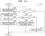
- FIG. 10 illustrates the example of the process at step S 200 in FIG. 9 .
- step S 200 operations at steps S 202 to S 208 for reading the target data of the read request from the main memory device 500 and operations at steps S 210 to S 216 for writing back the data to be evicted from the external cache 200 to the main memory device 500 are executed in parallel.
- the home agent 140 issues the read request to the main memory device 500 (for example, RD 5 in FIGS. 7 and 8 ).
- the home agent 140 stores the response data transferred from the main memory device 500 into the external cache 200 .
- the home agent 140 sets the inclusion valid flag EC-VAL of the target way of the entry in the TAGD 402 specified by the target address of the read request to “1”.
- the inclusion valid flag EC-VAL of “1” indicates that the target data of the read request RD is stored in both the LLC 30 and the external cache 200 and thus turns into the inclusion state.
- the home agent 140 responds to the LLC 30 that is the issuer of the read request with the target data of the read request transferred from the main memory device 500 at step S 208 , and ends the operations illustrated in FIG. 10 .
- the home agent 140 determines whether or not the dirty flag DRTY of the eviction target data included in a response from the external cache 200 is “1”. For example, the dirty flag DRTY is included in the response RTN 2 in FIGS. 7 and 8 .
- the home agent 140 performs step S 212 to execute the write-back.
- the dirty flag DRTY is “0”, the home agent 140 skips execution of the write-back, and thus ends the operations illustrated in FIG. 10 .
- the home agent 140 determines whether or not the flag WRBK-CPLT of the target way of the entry in the TAGD 402 specified by the target address of the read request is “1”.
- the flag WRBK-CPLT is “1”
- the address of the data in the modified state to be evicted from the LLC 30 is the same as the address of the data in the dirty state to be evicted from the external cache 200 .
- step S 214 the home agent 140 performs step S 214 in order to preferentially write back the data in the modified state to be evicted from the LLC 30 to the main memory device 500 .
- An operation of writing back data to be evicted from the LLC 30 to the main memory device 500 will be described with reference to FIG. 11 .
- the home agent 140 cancels the write back of the data from the external cache 200 to the main memory device 500 at step S 214 in order to preferentially perform the write back of the data from the LLC 30 to the main memory device 500 , and ends the operations illustrated in FIG. 10 .
- the home agent 140 writes back the data in the modified state evicted from the external cache to the main memory device 500 at step S 216 , and ends the operations illustrated in FIG. 10 .
- FIG. 11 is a diagram illustrating another example of an operation flow of the arithmetic processing device 100 in FIG. 1 .
- FIG. 11 illustrates an example of an arithmetic processing method of the arithmetic processing device 100 .
- Operations illustrated in FIG. 11 are started when an LLC 30 issues a write-back request WRBK by replacement to the home agent 140 based on a cache miss in the LLC 30 .
- FIG. 11 illustrates operations after the write-back request WRBK 1 in FIGS. 6 , 7 , and 8 is issued.
- the operations illustrated in FIG. 11 represent operations mainly performed by the home agent 140 .
- the write-back target data to be evicted from the LLC 30 is assumed to be in the modified state.
- the home agent 140 refers to the tag information of a way that holds eviction target data in the TAGD 402 , and determines whether or not the TAGD is in a hit state.
- the hit state of the TAGD indicates that the eviction target data is held in the data memory 302 of the LLC 30 .
- the home agent 140 performs step S 304 when the TAGD is in the hit state or performs step S 318 when the TAGD is not in the hit state.
- the home agent 140 determines whether or not the inclusion valid flag EC-VAL of the way that holds the eviction target data in the TAGD 402 is “1”. When the inclusion valid flag EC-VAL is “1”, the write-back target data is in the inclusion state and therefore the home agent 140 performs step S 306 in order to write back the data to the external cache 200 .
- the target data is in the non-inclusion state and therefore the home agent 140 performs step S 310 in order to write back the data to the main memory device 500 .
- the home agent 140 outputs, to the external cache 200 , information for setting the dirty flag DRTY of the entry having the data to be written back to “1” in the TAG 201 of the external cache 200 .
- the home agent 140 writes back the write-back target data to the external cache 200 at step S 308 , and ends the operations illustrated in FIG. 11 .
- the home agent 140 determines whether or not the eviction address of the LLC 30 matches the eviction address of the external cache 200 . When the eviction addresses match, the home agent 140 performs step S 312 in order to cancel the write-back from the external cache 200 to the main memory device 500 . When the eviction addresses do not match, the home agent 140 performs step S 314 in order to enable the write-back from the external cache 200 to the main memory device 500 .
- a match between the eviction addresses is determined when the tag address of an entry locked by the read request in the TAG 201 of the external cache 200 does not match the corresponding bits in the address of the read request.
- the home agent 140 sets the flag WRBK-CPLT of the target way of the entry in the TAGD 402 specified by the write-back target address to “1”. Thus, it is possible to cancel the write-back of the entry having the flag WRBK-CPLT set to “1” to the main memory device 500 , and to keep the write-back from being redundantly performed.
- the home agent 140 outputs, to the external cache 200 , information for setting the dirty flag DRTY of the entry having the data to be written back to “1” in the TAG 201 of the external cache 200 .
- the home agent 140 writes back the write-back target data in the LLC 30 to the main memory device 500 at step S 316 , and ends the operations illustrated in FIG. 11 .
- the home agent 140 detects the occurrence of a protocol error because there is no data to be evicted from the LLC 30 , and then ends the operations illustrated in FIG. 11 .
- the home agent 140 may notify a higher-level control device that manages the arithmetic processing device 100 of the occurrence of the protocol error.
- the inclusion valid flag EC-VAL indicating whether the data held in the LLC 30 is in the inclusion state or the non-inclusion state is provided in the TAGD 402 .
- the home agent 140 is able to determine a write-back location of the data held in the LLC 30 without reading the tag information from the TAG 201 of the external cache 200 . Since an access to the external cache 200 for determining the write-back location may be omitted, a degradation in the memory access efficiency may be suppressed. Accordingly, in the arithmetic processing device 100 including the caches in the hierarchical structure, a degradation in the cache access efficiency may be suppressed.
- the home agent 140 sets the inclusion valid flag EC-VAL to “1”.
- the home agent 140 resets the corresponding inclusion valid flag EC-VAL to “0”. Accordingly, the value of the inclusion valid flag EC-VAL may be changed in accordance with a change in the holding states of the data held in the LLC 30 and the external cache 200 . As a result, the home agent 140 is able to correctly write back the data from the LLC 30 by referring to the inclusion valid flag EC-VAL.
- the write-back completion flag WRBK-CPLT set when data corresponding to data written back from the LLC 30 to the main memory device 500 remains in the external cache 200 is provided in the TAGD 402 .
- the home agent 140 is able to cancel the write-back from the external cache 200 to the main memory device 500 . This makes it possible to keep the write-back operation for the same address from being performed twice and suppress a degradation in the cache access efficiency.
- a degradation in the cache access efficiency may be suppressed. It is possible to keep the data written back from the LLC 30 to the main memory device 500 from being overwritten with the old data from the external cache 200 , and to inhibit a malfunction of the arithmetic processing device 100 .
- the multiple LLCs 30 are coupled to the external cache 200 and the main memory device 500 via the home agent 140 .
- the home agent 140 is enabled to control data transfer between the multiple LLCs 30 and the external cache 200 and control data transfer between the multiple LLCs 30 and the main memory device 500 . Since each of the multiple LLCs 30 does not have to control data transfer to and from the external cache 200 and the main memory device 500 , the data transfer control by the cache operation may be simplified, and a degradation in the cache access efficiency may be suppressed.
- the home agent 140 With the TAGD 402 holding the information held in the LLC-TAG 303 of each LLC 30 , the home agent 140 is able to grasp the status of the data held in each LLC 30 . This makes it possible to reduce the frequency of accesses from the home agent 140 to each LLC 30 and suppress a degradation in the cache access efficiency.
- FIG. 12 illustrates an example of an arithmetic processing device according to another embodiment.
- An arithmetic processing device 100 A illustrated in FIG. 12 includes a die (semiconductor chip) 110 A and an external cache 200 , and has, for example, a package form.
- a main memory device 500 is coupled to the arithmetic processing device 100 A.
- the external cache 200 and the main memory device 500 are the same as or similar to the external cache 200 and the main memory device 500 illustrated in FIG. 1 , respectively.
- the arithmetic processing device 100 A and the main memory device 500 operate as an information processing device 600 A.
- the die 110 A includes an LLC block 120 A and memory control units 150 and 160 .
- the LLC block 120 A includes multiple cores 10 , a L1 cache 20 provided for each core 10 , and an LLC 30 A, and does not include the communication unit interface 40 illustrated in FIG. 1 .
- the cores 10 , the L1 caches 20 , and the memory control units 150 and 160 are the same as or similar to the cores 10 , the L1 caches 20 , and the memory control units 150 and 160 illustrated in FIG. 1 , respectively.
- the LLC 30 A employs a set associative scheme having multiple ways, and has multiple entries capable of respectively holding multiple pieces of data having the same index address.
- the LLC 30 A has an LLC-TAG 303 A (tag).
- An example of the LLC-TAG 303 A is illustrated in FIG. 13 .
- the LLC-TAG 303 A is an example of a first tag region and a second tag region.
- the LLC 30 A has a configuration and functions similar to those of the LLC 30 illustrated in FIG. 2 except that the LLC 30 A includes the LLC-TAG 303 A instead of the LLC-TAG 303 .
- the LLC 30 A includes a data buffer 301 , a data memory 302 , an eviction information holding unit 304 , multiple ports 305 , a pipe input unit 306 , a pipeline control unit 307 , a snoop lock unit 308 , and a cache miss control unit 309 , which are similar to those illustrated in FIG. 2 .
- the pipeline control unit 307 included in the LLC 30 A is an example of a control unit.
- FIG. 13 illustrates an example of constituent elements of the LLC-TAG 303 A in FIG. 12 .
- the elements that are the same as or similar to those illustrated in FIG. 5 will not be described in detail.
- the constituent elements of each entry in the external cache 200 are the same as or similar to those illustrated in FIG. 5 .
- a 1-bit inclusion valid flag EC-VAL and a 1-bit write-back completion flag WRBK-CPLT are added to the LLC-TAG 303 illustrated in FIG. 5 .
- the arithmetic processing device 100 A does not include multiple LLC blocks 120 .
- the arithmetic processing device 100 A does not include the home agent 140 illustrated in FIG. 1 , and the functions of the home agent 140 are implemented by the LLC block 120 A.
- the pipeline control unit 307 in the LLC 30 A has functions of setting the inclusion valid flag EC-VAL and the write-back completion flag WRBK-CPLT. Allocation of the index addresses in the LLC-TAG 303 A and the TAG 201 is the same as the allocation of the index addresses in the LLC-TAG 303 and the TAG 201 illustrated in FIG. 4 .
- FIG. 14 is a diagram illustrating an example of operations of the arithmetic processing device 100 A in FIG. 12 .
- the operations that are the same as or similar to those illustrated in FIG. 6 will not be described in detail.
- the operations illustrated in FIG. 14 are achieved by the arithmetic processing device 100 A executing an arithmetic processing method.
- FIG. 14 illustrates the operations in a case where a read request RD having caused a cache miss in the LLC 30 A causes a cache hit in the external cache 200 .
- the lock control is performed by the LLC 30 A.
- the operations in FIG. 14 are similar to the operations in FIG. 6 except that the LLC 30 A issues various requests to the external cache 200 , and responses from the external cache 200 are transferred to the LLC 30 A that is the issuer of the requests.
- FIG. 15 is a diagram illustrating another example of operations of the arithmetic processing device 100 A in FIG. 12 .
- the operations that are the same as or similar to those illustrated in FIG. 7 will not be described in detail.
- the operations illustrated in FIG. 15 are achieved by the arithmetic processing device 100 A executing an arithmetic processing method.
- FIG. 15 illustrates an example in which a read request RD having caused a cache miss in the LLC 30 A causes a cache miss in the external cache 200 and the data is read from the main memory device 500 .
- the write-back completion flag WRBK-CPLT of the write-back target entry is set to “0”.
- the lock control is performed by the LLC 30 A.
- the operations in FIG. 15 are similar to the operations illustrated in FIG. 7 except that the LLC 30 A issues various requests to the external cache 200 , and responses from the external cache 200 are transferred to the LLC 30 A that is the issuer of the requests.
- FIG. 16 is a diagram illustrating still another example of operations of the arithmetic processing device 100 A in FIG. 12 .
- the operations that are the same as or similar to those illustrated in FIG. 8 will not be described in detail.
- the operations illustrated in FIG. 16 are achieved by the arithmetic processing device 100 A executing an arithmetic processing method.
- FIG. 16 illustrates an example in which a read request RD having caused a cache miss in the LLC 30 A causes a cache miss in the external cache 200 and the data is read from the main memory device 500 .
- the write-back completion flag WRBK-CPLT of the write-back target entry is set to “1”.
- the lock control is performed by the LLC 30 A.
- the operations in FIG. 16 are similar to the operations in FIG. 8 except that the LLC 30 A issues various requests to the external cache 200 , and responses from the external cache 200 are transferred to the LLC 30 A that is the issuer of the requests.
- the LLC 30 A since the write-back completion flag WRBK-CPLT of the write-back target entry in the LLC-TAG 303 A is “1”, the LLC 30 A determines to cancel the write-back operation. Thus, it is possible to keep the write-back operation for the same address from being performed twice.
- An operation flow of the arithmetic processing device 100 A is similar to the operations in FIGS. 9 to 11 except that the LLC 30 A mainly performs the processes. In this embodiment, steps S 102 and S 104 in FIG. 9 are deleted.
- this embodiment is also capable of producing the effects similar to those in the foregoing embodiments.
- the LLC 30 A is able to determine the write-back location of the data held in the LLC 30 A without reading the tag information from the TAG 201 of the external cache 200 . Since an access to the external cache 200 for determining the write-back location may be omitted, a degradation in the memory access efficiency may be suppressed. Accordingly, in the arithmetic processing device 100 A including the caches in the hierarchical structure, a degradation in the cache access efficiency may be suppressed.
- the LLC 30 A is able to cancel the write-back from the external cache 200 to the main memory device 500 when the write-back completion flag WRBK-CPLT of the LLC-TAG 303 A is set. Thus, it is possible to keep the write-back operation for the same address from being performed twice, and to suppress a degradation in the cache access efficiency. It is also possible to keep the data written back from the LLC 30 A to the main memory device 500 from being overwritten with the old data from the external cache 200 , and to inhibit a malfunction of the arithmetic processing device 100 .
Landscapes
- Engineering & Computer Science (AREA)
- Theoretical Computer Science (AREA)
- Physics & Mathematics (AREA)
- General Engineering & Computer Science (AREA)
- General Physics & Mathematics (AREA)
- Memory System Of A Hierarchy Structure (AREA)
Abstract
Description
TAGD-HIT=(“LL-ST”!=“00”)&(RQ-PA[47:20]==“LL-TAG-AD”) (1)
EC-INDX-MCH=(“LL-ST”!=“00”)&(RQ-PA[32:20]==LL-TAG-AD(PA[32:20])) (2)
EC-VICTIM-HIT=(“LL-ST”!=“00”)&(RQ-PA[32:20]==LL-TAG-AD(PA [32:20]))&(RQ-PA[47:33]!=LL-TAG-AD(PA[47:33])) (3)
Claims (10)
Applications Claiming Priority (2)
| Application Number | Priority Date | Filing Date | Title |
|---|---|---|---|
| JP2022091656A JP2023178769A (en) | 2022-06-06 | 2022-06-06 | Arithmetic processing device and processing method |
| JP2022-091656 | 2022-06-06 |
Publications (2)
| Publication Number | Publication Date |
|---|---|
| US20230393988A1 US20230393988A1 (en) | 2023-12-07 |
| US12197342B2 true US12197342B2 (en) | 2025-01-14 |
Family
ID=88976757
Family Applications (1)
| Application Number | Title | Priority Date | Filing Date |
|---|---|---|---|
| US18/178,568 Active US12197342B2 (en) | 2022-06-06 | 2023-03-06 | Arithmetic processing device and arithmetic processing method |
Country Status (2)
| Country | Link |
|---|---|
| US (1) | US12197342B2 (en) |
| JP (1) | JP2023178769A (en) |
Families Citing this family (1)
| Publication number | Priority date | Publication date | Assignee | Title |
|---|---|---|---|---|
| CN114201120B (en) * | 2022-02-18 | 2022-05-10 | 苏州浪潮智能科技有限公司 | A data reading and writing method, device and related equipment |
Citations (15)
| Publication number | Priority date | Publication date | Assignee | Title |
|---|---|---|---|---|
| US5835941A (en) * | 1995-11-17 | 1998-11-10 | Micron Technology Inc. | Internally cached static random access memory architecture |
| US6502218B1 (en) * | 1999-12-16 | 2002-12-31 | Intel Corporation | Deferred correction of a single bit storage error in a cache tag array |
| US20030009622A1 (en) * | 2000-03-30 | 2003-01-09 | Ip-First, Llc | Method and apparatus for resolving additional load misses and page table walks under orthogonal stalls in a single pipeline processor |
| EP2634702A1 (en) * | 2012-02-29 | 2013-09-04 | Fujitsu Limited | Processor, information processing apparatus, and arithmetic method |
| US20150121011A1 (en) * | 2013-10-24 | 2015-04-30 | Mediatek Singapore Pte. Ltd. | Storage system having tag storage device with multiple tag entries associated with same data storage line for data recycling and related tag storage device |
| US20150178211A1 (en) * | 2012-09-07 | 2015-06-25 | Fujitsu Limited | Information processing apparatus, parallel computer system, and control method for controlling information processing apparatus |
| US20170212840A1 (en) | 2016-01-21 | 2017-07-27 | Qualcomm Incorporated | Providing scalable dynamic random access memory (dram) cache management using tag directory caches |
| US20170255562A1 (en) * | 2016-03-02 | 2017-09-07 | Kabushiki Kaisha Toshiba | Cache device and semiconductor device |
| US20170371793A1 (en) * | 2016-06-28 | 2017-12-28 | Arm Limited | Cache with compressed data and tag |
| JP2018018513A (en) | 2016-07-26 | 2018-02-01 | 三星電子株式会社Samsung Electronics Co.,Ltd. | Memory system, processing system, and method for operating memory stacks |
| US20190198083A1 (en) | 2016-06-27 | 2019-06-27 | Sukalpa Biswasw | Memory System Having Combined High Density, Low Bandwidth and Low Density, High Bandwidth Memories |
| US20200019499A1 (en) * | 2017-03-27 | 2020-01-16 | Mitsubishi Electric Corporation | Cache Memory and Method for Controlling the Same |
| US20200175646A1 (en) * | 2017-05-19 | 2020-06-04 | Movidius Ltd. | Methods, systems and apparatus to reduce memory latency when fetching pixel kernels |
| US20210248094A1 (en) * | 2020-02-07 | 2021-08-12 | Sunrise Memory Corporation | Quasi-volatile system-level memory |
| US20230236961A1 (en) * | 2022-01-10 | 2023-07-27 | Qualcomm Incorporated | Priority-Based Cache-Line Fitting in Compressed Memory Systems of Processor-Based Systems |
Family Cites Families (4)
| Publication number | Priority date | Publication date | Assignee | Title |
|---|---|---|---|---|
| US9021206B2 (en) * | 2011-08-25 | 2015-04-28 | International Business Machines Corporation | Use of cache statistics to ration cache hierarchy access |
| US9946646B2 (en) * | 2016-09-06 | 2018-04-17 | Advanced Micro Devices, Inc. | Systems and method for delayed cache utilization |
| US10430343B2 (en) * | 2017-02-21 | 2019-10-01 | Advanced Micro Devices, Inc. | Acceleration of cache-to-cache data transfers for producer-consumer communication |
| JP2022015514A (en) * | 2020-07-09 | 2022-01-21 | 富士通株式会社 | Semiconductor device |
-
2022
- 2022-06-06 JP JP2022091656A patent/JP2023178769A/en active Pending
-
2023
- 2023-03-06 US US18/178,568 patent/US12197342B2/en active Active
Patent Citations (18)
| Publication number | Priority date | Publication date | Assignee | Title |
|---|---|---|---|---|
| US5835941A (en) * | 1995-11-17 | 1998-11-10 | Micron Technology Inc. | Internally cached static random access memory architecture |
| US6502218B1 (en) * | 1999-12-16 | 2002-12-31 | Intel Corporation | Deferred correction of a single bit storage error in a cache tag array |
| US20030009622A1 (en) * | 2000-03-30 | 2003-01-09 | Ip-First, Llc | Method and apparatus for resolving additional load misses and page table walks under orthogonal stalls in a single pipeline processor |
| EP2634702A1 (en) * | 2012-02-29 | 2013-09-04 | Fujitsu Limited | Processor, information processing apparatus, and arithmetic method |
| US20150178211A1 (en) * | 2012-09-07 | 2015-06-25 | Fujitsu Limited | Information processing apparatus, parallel computer system, and control method for controlling information processing apparatus |
| US20150121011A1 (en) * | 2013-10-24 | 2015-04-30 | Mediatek Singapore Pte. Ltd. | Storage system having tag storage device with multiple tag entries associated with same data storage line for data recycling and related tag storage device |
| JP2019506671A (en) | 2016-01-21 | 2019-03-07 | クアルコム,インコーポレイテッド | Provide scalable dynamic random access memory (DRAM) cache management using tag directory cache |
| US20170212840A1 (en) | 2016-01-21 | 2017-07-27 | Qualcomm Incorporated | Providing scalable dynamic random access memory (dram) cache management using tag directory caches |
| US20170255562A1 (en) * | 2016-03-02 | 2017-09-07 | Kabushiki Kaisha Toshiba | Cache device and semiconductor device |
| US20190198083A1 (en) | 2016-06-27 | 2019-06-27 | Sukalpa Biswasw | Memory System Having Combined High Density, Low Bandwidth and Low Density, High Bandwidth Memories |
| JP2019520636A (en) | 2016-06-27 | 2019-07-18 | アップル インコーポレイテッドApple Inc. | Memory system combining high density low bandwidth memory and low density high bandwidth memory |
| US20170371793A1 (en) * | 2016-06-28 | 2017-12-28 | Arm Limited | Cache with compressed data and tag |
| US20180032437A1 (en) | 2016-07-26 | 2018-02-01 | Samsung Electronics Co., Ltd. | Hbm with in-memory cache manager |
| JP2018018513A (en) | 2016-07-26 | 2018-02-01 | 三星電子株式会社Samsung Electronics Co.,Ltd. | Memory system, processing system, and method for operating memory stacks |
| US20200019499A1 (en) * | 2017-03-27 | 2020-01-16 | Mitsubishi Electric Corporation | Cache Memory and Method for Controlling the Same |
| US20200175646A1 (en) * | 2017-05-19 | 2020-06-04 | Movidius Ltd. | Methods, systems and apparatus to reduce memory latency when fetching pixel kernels |
| US20210248094A1 (en) * | 2020-02-07 | 2021-08-12 | Sunrise Memory Corporation | Quasi-volatile system-level memory |
| US20230236961A1 (en) * | 2022-01-10 | 2023-07-27 | Qualcomm Incorporated | Priority-Based Cache-Line Fitting in Compressed Memory Systems of Processor-Based Systems |
Non-Patent Citations (3)
| Title |
|---|
| F. Hameed, A. A. Khan and J. Castrillon, "Improving the Performance of Block-based Dram Caches Via Tag-Data Decoupling," in IEEE Transactions on Computers, vol. 70, No. 11, pp. 1914-1927, Nov. 1, 2021. * |
| Hong Wan, Tong Sun and Qing Yang, "CAT—caching address tags—a technique for reducing area cost of on-chip caches," Proceedings 22nd Annual International Symposium on Computer Architecture, Santa Margherita Ligure, Italy, 1995, pp. 381-390. * |
| S.-F. Hsiao, S.-Y. Lin, T.-C. Cheng and M.-Y. Tsai, "An Automatic Cache Generator Based on Content-Addressable Memory," APCCAS 2006—2006 IEEE Asia Pacific Conference on Circuits and Systems, Singapore, 2006, pp. 1313-1316. * |
Also Published As
| Publication number | Publication date |
|---|---|
| JP2023178769A (en) | 2023-12-18 |
| US20230393988A1 (en) | 2023-12-07 |
Similar Documents
| Publication | Publication Date | Title |
|---|---|---|
| US8782348B2 (en) | Microprocessor cache line evict array | |
| US7698508B2 (en) | System and method for reducing unnecessary cache operations | |
| US9170946B2 (en) | Directory cache supporting non-atomic input/output operations | |
| US7305522B2 (en) | Victim cache using direct intervention | |
| US7305523B2 (en) | Cache memory direct intervention | |
| US7467323B2 (en) | Data processing system and method for efficient storage of metadata in a system memory | |
| US20060179247A1 (en) | Data processing system and method for efficient communication utilizing an Ig coherency state | |
| JP4447580B2 (en) | Partitioned sparse directory for distributed shared memory multiprocessor systems | |
| US6973547B2 (en) | Coherence message prediction mechanism and multiprocessing computer system employing the same | |
| US7281092B2 (en) | System and method of managing cache hierarchies with adaptive mechanisms | |
| US20140289469A1 (en) | Processor and control method of processor | |
| US7117312B1 (en) | Mechanism and method employing a plurality of hash functions for cache snoop filtering | |
| US7325102B1 (en) | Mechanism and method for cache snoop filtering | |
| US7577793B2 (en) | Patrol snooping for higher level cache eviction candidate identification | |
| US7454577B2 (en) | Data processing system and method for efficient communication utilizing an Tn and Ten coherency states | |
| US6715040B2 (en) | Performance improvement of a write instruction of a non-inclusive hierarchical cache memory unit | |
| US8473685B2 (en) | Cache memory device, processor, and control method for cache memory device to reduce power unnecessarily consumed by cache memory | |
| US12197342B2 (en) | Arithmetic processing device and arithmetic processing method | |
| JP2007200292A (en) | Disowning cache entries on aging out of the entry | |
| US7353341B2 (en) | System and method for canceling write back operation during simultaneous snoop push or snoop kill operation in write back caches | |
| US6839806B2 (en) | Cache system with a cache tag memory and a cache tag buffer | |
| US7797495B1 (en) | Distributed directory cache | |
| US9053030B2 (en) | Cache memory and control method thereof with cache hit rate | |
| JP5319049B2 (en) | Cash system | |
| US9430397B2 (en) | Processor and control method thereof |
Legal Events
| Date | Code | Title | Description |
|---|---|---|---|
| AS | Assignment |
Owner name: FUJITSU LIMITED, JAPAN Free format text: ASSIGNMENT OF ASSIGNORS INTEREST;ASSIGNOR:HIKICHI, TORU;REEL/FRAME:062885/0337 Effective date: 20230125 |
|
| FEPP | Fee payment procedure |
Free format text: ENTITY STATUS SET TO UNDISCOUNTED (ORIGINAL EVENT CODE: BIG.); ENTITY STATUS OF PATENT OWNER: LARGE ENTITY |
|
| STPP | Information on status: patent application and granting procedure in general |
Free format text: DOCKETED NEW CASE - READY FOR EXAMINATION |
|
| STPP | Information on status: patent application and granting procedure in general |
Free format text: NON FINAL ACTION MAILED |
|
| STPP | Information on status: patent application and granting procedure in general |
Free format text: RESPONSE TO NON-FINAL OFFICE ACTION ENTERED AND FORWARDED TO EXAMINER |
|
| STPP | Information on status: patent application and granting procedure in general |
Free format text: NOTICE OF ALLOWANCE MAILED -- APPLICATION RECEIVED IN OFFICE OF PUBLICATIONS |
|
| STPP | Information on status: patent application and granting procedure in general |
Free format text: PUBLICATIONS -- ISSUE FEE PAYMENT RECEIVED |
|
| STPP | Information on status: patent application and granting procedure in general |
Free format text: PUBLICATIONS -- ISSUE FEE PAYMENT VERIFIED |
|
| STCF | Information on status: patent grant |
Free format text: PATENTED CASE |