US12193337B2 - Semiconductor device and method of fabricating the same - Google Patents
Semiconductor device and method of fabricating the same Download PDFInfo
- Publication number
- US12193337B2 US12193337B2 US16/991,055 US202016991055A US12193337B2 US 12193337 B2 US12193337 B2 US 12193337B2 US 202016991055 A US202016991055 A US 202016991055A US 12193337 B2 US12193337 B2 US 12193337B2
- Authority
- US
- United States
- Prior art keywords
- layer
- dielectric layer
- conductive line
- memory element
- dual damascene
- Prior art date
- Legal status (The legal status is an assumption and is not a legal conclusion. Google has not performed a legal analysis and makes no representation as to the accuracy of the status listed.)
- Active, expires
Links
- 239000004065 semiconductor Substances 0.000 title claims abstract description 20
- 238000004519 manufacturing process Methods 0.000 title abstract description 8
- 239000000758 substrate Substances 0.000 claims abstract description 24
- 229910052751 metal Inorganic materials 0.000 claims description 34
- 239000002184 metal Substances 0.000 claims description 34
- 230000009977 dual effect Effects 0.000 claims description 24
- 239000010410 layer Substances 0.000 description 137
- 238000000034 method Methods 0.000 description 25
- 239000011229 interlayer Substances 0.000 description 22
- 239000000463 material Substances 0.000 description 17
- 230000004888 barrier function Effects 0.000 description 12
- 239000004020 conductor Substances 0.000 description 9
- 238000005530 etching Methods 0.000 description 7
- VYPSYNLAJGMNEJ-UHFFFAOYSA-N Silicium dioxide Chemical compound O=[Si]=O VYPSYNLAJGMNEJ-UHFFFAOYSA-N 0.000 description 5
- 238000002161 passivation Methods 0.000 description 5
- 230000002093 peripheral effect Effects 0.000 description 5
- 229910052814 silicon oxide Inorganic materials 0.000 description 5
- 229910052581 Si3N4 Inorganic materials 0.000 description 4
- 229910021332 silicide Inorganic materials 0.000 description 4
- FVBUAEGBCNSCDD-UHFFFAOYSA-N silicide(4-) Chemical compound [Si-4] FVBUAEGBCNSCDD-UHFFFAOYSA-N 0.000 description 4
- HQVNEWCFYHHQES-UHFFFAOYSA-N silicon nitride Chemical compound N12[Si]34N5[Si]62N3[Si]51N64 HQVNEWCFYHHQES-UHFFFAOYSA-N 0.000 description 4
- 230000008901 benefit Effects 0.000 description 3
- 238000002955 isolation Methods 0.000 description 3
- BOTDANWDWHJENH-UHFFFAOYSA-N Tetraethyl orthosilicate Chemical compound CCO[Si](OCC)(OCC)OCC BOTDANWDWHJENH-UHFFFAOYSA-N 0.000 description 2
- MCMNRKCIXSYSNV-UHFFFAOYSA-N Zirconium dioxide Chemical compound O=[Zr]=O MCMNRKCIXSYSNV-UHFFFAOYSA-N 0.000 description 2
- 239000004411 aluminium Substances 0.000 description 2
- 229910052782 aluminium Inorganic materials 0.000 description 2
- XAGFODPZIPBFFR-UHFFFAOYSA-N aluminium Chemical compound [Al] XAGFODPZIPBFFR-UHFFFAOYSA-N 0.000 description 2
- 238000005229 chemical vapour deposition Methods 0.000 description 2
- 238000005516 engineering process Methods 0.000 description 2
- 238000007517 polishing process Methods 0.000 description 2
- 239000000126 substance Substances 0.000 description 2
- RYGMFSIKBFXOCR-UHFFFAOYSA-N Copper Chemical compound [Cu] RYGMFSIKBFXOCR-UHFFFAOYSA-N 0.000 description 1
- RTAQQCXQSZGOHL-UHFFFAOYSA-N Titanium Chemical compound [Ti] RTAQQCXQSZGOHL-UHFFFAOYSA-N 0.000 description 1
- NRTOMJZYCJJWKI-UHFFFAOYSA-N Titanium nitride Chemical compound [Ti]#N NRTOMJZYCJJWKI-UHFFFAOYSA-N 0.000 description 1
- PNEYBMLMFCGWSK-UHFFFAOYSA-N aluminium oxide Inorganic materials [O-2].[O-2].[O-2].[Al+3].[Al+3] PNEYBMLMFCGWSK-UHFFFAOYSA-N 0.000 description 1
- 230000000295 complement effect Effects 0.000 description 1
- 229910052802 copper Inorganic materials 0.000 description 1
- 239000010949 copper Substances 0.000 description 1
- 239000011521 glass Substances 0.000 description 1
- 229910000449 hafnium oxide Inorganic materials 0.000 description 1
- WIHZLLGSGQNAGK-UHFFFAOYSA-N hafnium(4+);oxygen(2-) Chemical compound [O-2].[O-2].[Hf+4] WIHZLLGSGQNAGK-UHFFFAOYSA-N 0.000 description 1
- 239000012212 insulator Substances 0.000 description 1
- 229910044991 metal oxide Inorganic materials 0.000 description 1
- 150000004706 metal oxides Chemical class 0.000 description 1
- 238000012986 modification Methods 0.000 description 1
- 230000004048 modification Effects 0.000 description 1
- 238000005240 physical vapour deposition Methods 0.000 description 1
- 229910052710 silicon Inorganic materials 0.000 description 1
- 239000010703 silicon Substances 0.000 description 1
- 229910010271 silicon carbide Inorganic materials 0.000 description 1
- -1 silicon carbide nitride Chemical class 0.000 description 1
- 239000002356 single layer Substances 0.000 description 1
- 239000010936 titanium Substances 0.000 description 1
- 229910052719 titanium Inorganic materials 0.000 description 1
- WFKWXMTUELFFGS-UHFFFAOYSA-N tungsten Chemical compound [W] WFKWXMTUELFFGS-UHFFFAOYSA-N 0.000 description 1
- 229910052721 tungsten Inorganic materials 0.000 description 1
- 239000010937 tungsten Substances 0.000 description 1
Images


Classifications
-
- H—ELECTRICITY
- H10—SEMICONDUCTOR DEVICES; ELECTRIC SOLID-STATE DEVICES NOT OTHERWISE PROVIDED FOR
- H10B—ELECTRONIC MEMORY DEVICES
- H10B63/00—Resistance change memory devices, e.g. resistive RAM [ReRAM] devices
- H10B63/30—Resistance change memory devices, e.g. resistive RAM [ReRAM] devices comprising selection components having three or more electrodes, e.g. transistors
-
- H—ELECTRICITY
- H10—SEMICONDUCTOR DEVICES; ELECTRIC SOLID-STATE DEVICES NOT OTHERWISE PROVIDED FOR
- H10N—ELECTRIC SOLID-STATE DEVICES NOT OTHERWISE PROVIDED FOR
- H10N50/00—Galvanomagnetic devices
- H10N50/80—Constructional details
-
- H—ELECTRICITY
- H10—SEMICONDUCTOR DEVICES; ELECTRIC SOLID-STATE DEVICES NOT OTHERWISE PROVIDED FOR
- H10B—ELECTRONIC MEMORY DEVICES
- H10B61/00—Magnetic memory devices, e.g. magnetoresistive RAM [MRAM] devices
- H10B61/20—Magnetic memory devices, e.g. magnetoresistive RAM [MRAM] devices comprising components having three or more electrodes, e.g. transistors
- H10B61/22—Magnetic memory devices, e.g. magnetoresistive RAM [MRAM] devices comprising components having three or more electrodes, e.g. transistors of the field-effect transistor [FET] type
-
- H—ELECTRICITY
- H10—SEMICONDUCTOR DEVICES; ELECTRIC SOLID-STATE DEVICES NOT OTHERWISE PROVIDED FOR
- H10N—ELECTRIC SOLID-STATE DEVICES NOT OTHERWISE PROVIDED FOR
- H10N50/00—Galvanomagnetic devices
- H10N50/01—Manufacture or treatment
Definitions
- the disclosure relates to an integrated circuit and a method of fabricating the same, and in particular, to a semiconductor device and a method of fabricating the same.
- resistive memory for example, resistive random access memory (RRAM)
- RRAM resistive random access memory
- CMOS complementary metal oxide semiconductor
- a depth of one via on the resistive memory is different from a depth of an adjacent via.
- different via depths may easily cause etching problems, or cause different via sizes and even cause the problems of excessively high contact resistance and the like.
- Embodiments of the invention provide a semiconductor device and a method of fabricating the same.
- the etching problems, different via sizes and the problems of excessively high contact resistance and the like caused by different depths of a via connecting a memory cell and a via connecting a conductor layer may be avoided.
- the embodiments of the invention provide a method of fabricating a semiconductor device, which includes the following steps: forming a plurality of doped regions in a substrate; forming a first dielectric layer on the substrate; forming a plurality of first contacts and second contacts in the first dielectric layer to connect to the plurality of doped regions; forming a memory element on the first dielectric layer, the memory element being electrically connected to the second contact; forming a second dielectric layer on the first dielectric layer, the second dielectric layer surrounding the memory element; and forming a conductive line in the second dielectric layer, a top surface of the conductive line being at a same level as a top surface of the memory element, and the conductive line being electrically connected to the plurality of first contacts.
- vias connecting a memory cell and connecting a conductor layer are the same in depth, so that the depths and sizes of the vias may be effectively controlled, and contact resistance may be reduced.
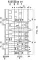
- FIG. 1 A to FIG. 1 G are cross-sectional views of a process for fabricating a semiconductor device according to an embodiment of the invention.
- FIG. 2 is a top view of a semiconductor device according to an embodiment of the invention.
- FIG. 3 is a cross-sectional view of a semiconductor device according to another embodiment of the invention.
- the substrate 10 may be a semiconductor substrate 10 or a silicon on insulator (SOI) substrate 10 .
- the substrate 10 may include a memory cell region CR and a peripheral region PR.
- the memory cell region CR is also called an array region.
- a plurality of isolation structures ST and a plurality of first transistors T 1 and second transistors T 2 are formed in the memory cell region CR and the peripheral region PR.
- Materials for the isolation structures ST include silicon oxide.
- the isolation structures ST define an active region AA 1 in the substrate 10 in the memory cell region CR and define an active region AA 2 in the substrate 10 in the peripheral region PR.
- the first etch stop layer 12 is, for example, a silicon nitride layer.
- the first inter-layer dielectric layer 20 sequentially includes, for example, a first dielectric layer 14 and a second dielectric layer 16 .
- the first dielectric layer 14 is, for example, undoped spin-on glass.
- the second dielectric layer 16 is, for example, a flat layer formed by planarizing silicon oxide formed from tetraethoxysilane (TEOS) as a gas source through a planarization process.
- TEOS tetraethoxysilane
- contacts 30 a 1 and 30 a 2 being in contact with first metal silicide layers Sa 1 of the first transistors T 1 are formed in the first inter-layer dielectric layer 20 and the first etch stop layer 12 of the memory cell region CR, and contacts 30 b being in contact with second metal silicide layers Sa 2 of the second transistors T 2 are formed in the first inter-layer dielectric layer 20 of the peripheral region PR.
- memory elements 50 are formed on the substrate 10 , as shown in FIG. 1 B .
- the memory elements 50 are located on the substrate 10 in the memory cell region CR.
- the memory elements 50 are electrically connected to drain regions D 1 of the first transistors T 1 through the contacts 30 a 2 .
- the memory element 50 may be a resistive memory or a magneto-resistive memory, etc.
- the memory element 50 includes a first electrode layer 32 , an insulating layer 34 , a second electrode layer 40 and a top cover layer 42 .
- a barrier layer 58 and a second inter-layer dielectric layer 60 are formed on the memory element 50 and the first inter-layer dielectric layer 20 .
- a material for the barrier layer 58 is, for example, titanium oxynitride, alumina, hafnium oxide, zirconia or a combination thereof.
- the second inter-layer dielectric layer 60 may be, for example, a silicon oxide layer.
- a planarization process is executed on the second inter-layer dielectric layer 60 to form a second inter-layer dielectric layer 60 a with a flat surface.
- the second inter-layer dielectric layer 60 a surrounds the memory elements 50 .
- a top surface of the second inter-layer dielectric layer 60 a and a top surface of the barrier layer 58 are coplanar with top surfaces of the top cover layers 42 .
- a first conductive line 72 a is formed in the second inter-layer dielectric layer 60 a and the barrier layer 58 in the memory cell region CR, and a first conductive line 72 b is formed in the second inter-layer dielectric layer 60 a in the peripheral region PR.
- the first conductive lines 72 a and 72 b are formed by the following method.
- a first conductive line channel 71 a and a first conductive line channel 71 b are formed in the second inter-layer dielectric layer 60 a and the barrier layer 58 through a lithographic anisotropic etching process. Then, a barrier material layer and a conductor material layer are formed on the first conductive line channel 71 a , the first conductive line channel 71 b and the second inter-layer dielectric layer 60 a .
- the barrier material layer is, for example, titanium nitride formed by a chemical vapor deposition method.
- the conductor material layer is, for example, tungsten, aluminium, copper or a combination thereof formed by a physical vapor deposition method.
- a chemical mechanical polishing process or an etching-back process is executed to remove the barrier material layer and the conductor material layer from the second inter-layer dielectric layer 60 a , and in the first conductive line channels 71 a and 71 b , a first barrier layer 68 and a first conductor layer 70 are formed and the first conductive lines 72 a and 72 b are formed respectively.
- the first conductive line 72 a and the first conductive line 72 b are together referred to as a first metal layer M 1 .
- the first conductive line 72 a and the first conductive line 72 b are lines or path lines extending along an XY plane. That is, the first conductive line 72 a and the first conductive line 72 b are substantially parallel to a surface of the substrate 10 and substantially perpendicular to a normal of the substrate 10 .
- the first conductive line 72 a and the first conductive line 72 b are arranged at the same level as the memory elements 50 .
- the same level refers to the fact that top surfaces of the first conductive line 72 a and the first conductive line 72 b and top surfaces of the memory elements 50 are at the same level or substantially located on the same plane, or refers to the fact that bottom surfaces of the first conductive line 72 a and the first conductive line 72 b and bottom surfaces of the memory elements 50 are at the same level or substantially located on the same plane.
- the first conductive line channel 71 a and the first conductive line channel 71 b are formed, excessive etching may be performed, and thus the bottom surfaces of the first conductive line 72 a and the first conductive line 72 b may be slightly lower than the bottom surfaces of the memory elements 50 .
- heights H 1 a and H 1 b of the first conductive line 72 a and the first conductive line 72 b may be equal to or slightly greater than heights H 2 of the memory elements 50 .
- a cross-sectional view along a section line I-I′ in FIG. 2 is shown by the memory cell region CR in FIG. 1 D .
- a plurality of first conductive lines 72 a and a plurality of memory elements 50 are provided on the substrate 10 .
- Patterns of the first conductive lines 72 a are different from patterns of the memory elements 50 .
- each memory element 50 is blocky or island-shaped and is in physical contact with a single contact 30 a 2 ; and each first conductive line 72 a is double-row comb-shaped and may be in physical contact with a plurality of contacts 30 a 1 .
- Each first conductive line 72 a may include a main line portion P 1 and a plurality of extending portions P 2 .
- the main line portion P 1 extends along a first direction (for example, a Y-axis direction).
- a length of the main line portion P 1 is several to dozens of times a length of the memory element 50 .
- Each extending portion P 2 extends along a second direction (for example, an X-axis direction) and is arranged along the first direction, penetrated through by the main line portion P 1 and connected to the main line portion P 1 .
- Each extending portion P 2 is in contact with two contacts 30 a 1 , and each contact 30 a 1 is electrically connected to the first metal silicide layer Sa 1 on a source region 51 shared by two first transistors T 1 below.
- the memory elements 50 may be arranged in an array.
- the memory elements 50 (for example, 50 e and 50 a ) are arranged on two sides of the main line portions P 1 .
- every two adjacent memory elements 50 (for example, 50 a and 50 c ) are arranged alternately with the main line portions P 1 .
- every two adjacent memory elements 50 (for example, 50 a and 50 b ) are arranged alternately with the extending portions P 2 .
- the plurality of main line portions P 1 of the plurality of first conductive lines 72 a is arranged in parallel with one another.
- the plurality of extending portions P 2 of the plurality of conductive lines 72 a may be aligned with one another and arranged into a plurality of line segments extending along the second direction.
- the plurality of main line portions P 1 and the plurality of extending portions P 2 of the plurality of first conductive lines 72 a may be arranged into a chessboard.
- a checker A of the chessboard is defined by two adjacent main line portions P 1 and two adjacent extending portions P 2 of each of the two main line portions P 1 .
- each checker A Four adjacent memory elements 50 (for example, 50 a , 50 b , 50 c and 50 d ) are arranged in each checker A.
- the four adjacent memory elements 50 are electrically connected to the first metal silicide layers Sa 1 on the drain regions D 1 of four first transistors T 1 through four contacts 30 a 2 .
- a second etch stop layer 74 and a first inter-metal dielectric layer 76 are formed on the substrate 10 .
- the second etch stop layer 74 is, for example, a silicon carbide nitride (SiCN) layer.
- the first inter-metal dielectric layer 76 may be a single layer or multiple layers.
- the first inter-metal dielectric layer 76 is, for example, a silicon oxide layer formed by a chemical vapor deposition process and planarized by a planarization process.
- part of the first inter-metal dielectric layer 76 is etched to be removed by taking the second etch stop layer 74 as an etch stop layer
- part of the second etch stop layer 74 is removed to expose the first conductive line 72 a , the top cover layers 42 of the memory elements 50 and the first conductive line 72 b .
- part of the top cover layers 42 are continued to be etched to form dual damascene openings 78 a 1 , 78 a 2 and 78 b .
- the first conductive line 72 a and the first conductive line 72 b are hardly etched or only very small parts are etched.
- an etching process for forming via openings of the dual damascene openings 78 a 2 located on the memory elements and via openings of the dual damascene openings 78 a 1 and 78 b located on the first conductive lines may be controlled by a single step.
- the dual damascene openings 78 a 1 , 78 a 2 and 78 b expose the first conductive line 72 a , the second electrode layers 40 of the memory elements 50 and the first conductive line 72 b respectively.
- the barrier material layers and the conductor material layers are formed in the dual damascene openings 78 a 1 , 78 a 2 and 78 b .
- a chemical mechanical polishing process or an etching-back process is executed to remove the barrier material layer and the conductive material layer from the first inter-metal dielectric layer 76 , and second barrier layers 88 and second conductor layers 90 left in the dual damascene openings 78 a 1 , 78 a 2 and 78 b form dual damascene structures 80 a 1 , 80 a 2 and 80 b respectively.
- the height H 3 of the first via 82 a 1 and the height H 4 of the first via 82 a 2 may not be too great and the first vias 82 a still have enough bottom widths, contact resistance between the first via 82 a 1 and the first conductive line 72 a or between the first via 82 a and the memory element 50 is quite low.
Landscapes
- Engineering & Computer Science (AREA)
- Manufacturing & Machinery (AREA)
- Internal Circuitry In Semiconductor Integrated Circuit Devices (AREA)
- Semiconductor Memories (AREA)
Abstract
Description
Claims (6)
Priority Applications (1)
| Application Number | Priority Date | Filing Date | Title |
|---|---|---|---|
| US18/945,580 US20250072295A1 (en) | 2019-08-22 | 2024-11-13 | Method of fabricating semiconductor device |
Applications Claiming Priority (2)
| Application Number | Priority Date | Filing Date | Title |
|---|---|---|---|
| TW108130117 | 2019-08-22 | ||
| TW108130117A TWI722546B (en) | 2019-08-22 | 2019-08-22 | Semiconductor device and method of fabricating the same |
Related Child Applications (1)
| Application Number | Title | Priority Date | Filing Date |
|---|---|---|---|
| US18/945,580 Division US20250072295A1 (en) | 2019-08-22 | 2024-11-13 | Method of fabricating semiconductor device |
Publications (2)
| Publication Number | Publication Date |
|---|---|
| US20210057640A1 US20210057640A1 (en) | 2021-02-25 |
| US12193337B2 true US12193337B2 (en) | 2025-01-07 |
Family
ID=74646063
Family Applications (2)
| Application Number | Title | Priority Date | Filing Date |
|---|---|---|---|
| US16/991,055 Active 2041-01-08 US12193337B2 (en) | 2019-08-22 | 2020-08-12 | Semiconductor device and method of fabricating the same |
| US18/945,580 Pending US20250072295A1 (en) | 2019-08-22 | 2024-11-13 | Method of fabricating semiconductor device |
Family Applications After (1)
| Application Number | Title | Priority Date | Filing Date |
|---|---|---|---|
| US18/945,580 Pending US20250072295A1 (en) | 2019-08-22 | 2024-11-13 | Method of fabricating semiconductor device |
Country Status (2)
| Country | Link |
|---|---|
| US (2) | US12193337B2 (en) |
| TW (1) | TWI722546B (en) |
Cited By (1)
| Publication number | Priority date | Publication date | Assignee | Title |
|---|---|---|---|---|
| US20240049445A1 (en) * | 2022-08-02 | 2024-02-08 | Samsung Electronics Co., Ltd. | Methods of manufacturing semiconductor devices |
Citations (10)
| Publication number | Priority date | Publication date | Assignee | Title |
|---|---|---|---|---|
| US20030030084A1 (en) | 2001-08-08 | 2003-02-13 | Ted Moise | Fabricating an embedded ferroelectric memory cell |
| CN100428477C (en) | 2002-11-18 | 2008-10-22 | 富士通株式会社 | Semiconductor device and manufacturing method thereof |
| TW200939458A (en) | 2007-11-29 | 2009-09-16 | Renesas Tech Corp | Semiconductor device and method of manufacturing the same |
| US20140061573A1 (en) * | 2011-09-27 | 2014-03-06 | Panasonic Corporation | Nonvolatile memory element, nonvolatile memory device, and methods of manufacturing the same |
| US20170084820A1 (en) * | 2015-09-23 | 2017-03-23 | Globalfoundries Singapore Pte. Ltd. | Integrated magnetic random access memory with logic device |
| US20170092692A1 (en) * | 2015-09-30 | 2017-03-30 | Taiwan Semiconductor Manufacturing Company Ltd. | Semiconductor structure integrated with magnetic tunneling junction and manufacturing method thereof |
| CN107039483A (en) | 2015-11-27 | 2017-08-11 | 台湾积体电路制造股份有限公司 | Semiconductor structure and forming method thereof |
| US20180040817A1 (en) * | 2016-08-08 | 2018-02-08 | Taiwan Semiconductor Manufacturing Co., Ltd. | Embedded memory device between noncontigous interconnect metal layers |
| US10163981B2 (en) * | 2016-04-27 | 2018-12-25 | Taiwan Semiconductor Manufacturing Co., Ltd. | Metal landing method for RRAM technology |
| US20180374895A1 (en) * | 2017-06-27 | 2018-12-27 | Taiwan Semiconductor Manufacturing Company Ltd. | Semiconductor structure and method of forming the same |
-
2019
- 2019-08-22 TW TW108130117A patent/TWI722546B/en active
-
2020
- 2020-08-12 US US16/991,055 patent/US12193337B2/en active Active
-
2024
- 2024-11-13 US US18/945,580 patent/US20250072295A1/en active Pending
Patent Citations (13)
| Publication number | Priority date | Publication date | Assignee | Title |
|---|---|---|---|---|
| US20030030084A1 (en) | 2001-08-08 | 2003-02-13 | Ted Moise | Fabricating an embedded ferroelectric memory cell |
| CN100428477C (en) | 2002-11-18 | 2008-10-22 | 富士通株式会社 | Semiconductor device and manufacturing method thereof |
| TW200939458A (en) | 2007-11-29 | 2009-09-16 | Renesas Tech Corp | Semiconductor device and method of manufacturing the same |
| US20140061573A1 (en) * | 2011-09-27 | 2014-03-06 | Panasonic Corporation | Nonvolatile memory element, nonvolatile memory device, and methods of manufacturing the same |
| US20170084820A1 (en) * | 2015-09-23 | 2017-03-23 | Globalfoundries Singapore Pte. Ltd. | Integrated magnetic random access memory with logic device |
| CN106876423A (en) | 2015-09-30 | 2017-06-20 | 台湾积体电路制造股份有限公司 | Semiconductor structure integrated with magnetic tunnel junction and method of manufacturing the same |
| US20170092692A1 (en) * | 2015-09-30 | 2017-03-30 | Taiwan Semiconductor Manufacturing Company Ltd. | Semiconductor structure integrated with magnetic tunneling junction and manufacturing method thereof |
| TW201724490A (en) | 2015-09-30 | 2017-07-01 | 台灣積體電路製造股份有限公司 | Semiconductor structure integrated with magnetic tunnel junction and manufacturing method thereof |
| CN107039483A (en) | 2015-11-27 | 2017-08-11 | 台湾积体电路制造股份有限公司 | Semiconductor structure and forming method thereof |
| TW201729414A (en) | 2015-11-27 | 2017-08-16 | 台灣積體電路製造股份有限公司 | Semiconductor structure and method of forming the same |
| US10163981B2 (en) * | 2016-04-27 | 2018-12-25 | Taiwan Semiconductor Manufacturing Co., Ltd. | Metal landing method for RRAM technology |
| US20180040817A1 (en) * | 2016-08-08 | 2018-02-08 | Taiwan Semiconductor Manufacturing Co., Ltd. | Embedded memory device between noncontigous interconnect metal layers |
| US20180374895A1 (en) * | 2017-06-27 | 2018-12-27 | Taiwan Semiconductor Manufacturing Company Ltd. | Semiconductor structure and method of forming the same |
Non-Patent Citations (1)
| Title |
|---|
| "Office Action of China Counterpart Application", issued on May 31, 2023, p. 1-p. 7. |
Cited By (1)
| Publication number | Priority date | Publication date | Assignee | Title |
|---|---|---|---|---|
| US20240049445A1 (en) * | 2022-08-02 | 2024-02-08 | Samsung Electronics Co., Ltd. | Methods of manufacturing semiconductor devices |
Also Published As
| Publication number | Publication date |
|---|---|
| TWI722546B (en) | 2021-03-21 |
| US20250072295A1 (en) | 2025-02-27 |
| TW202109760A (en) | 2021-03-01 |
| US20210057640A1 (en) | 2021-02-25 |
Similar Documents
| Publication | Publication Date | Title |
|---|---|---|
| US8247291B2 (en) | Methods of forming fine patterns in integrated circuit devices and methods of manufacturing integrated circuit devices including the same | |
| KR20100092239A (en) | Semiconductor device and method of manufacturing the semiconductor device | |
| TW201810591A (en) | Semiconductor device and method of forming same | |
| US8513809B2 (en) | Semiconductor device | |
| CN106941091B (en) | Interconnect structure, interconnect layout structure and method for fabricating the same | |
| KR100626378B1 (en) | Wiring structure of semiconductor device and method of forming the same | |
| CN101009267A (en) | Semiconductor device having self-aligned contact and method of fabricating the same | |
| JP2012199381A (en) | Semiconductor device and method of manufacturing the same | |
| TWI550778B (en) | Semiconductor structure | |
| KR100791339B1 (en) | Composite chip semiconductor device including planarization resistance pattern and manufacturing method | |
| US9627468B2 (en) | Capacitor structure and method of manufacturing the same | |
| US20230045420A1 (en) | Semiconductor structure and method of forming the same | |
| US20250072295A1 (en) | Method of fabricating semiconductor device | |
| US7829925B2 (en) | Semiconductor device and method for manufacturing same | |
| US20100140747A1 (en) | Semiconductor devices | |
| JP2008010737A (en) | Semiconductor device and manufacturing method thereof | |
| KR20110137227A (en) | Manufacturing Method of Semiconductor Device | |
| JP2016046269A (en) | Semiconductor device and method for manufacturing semiconductor device | |
| US20080067692A1 (en) | Semiconductor devices having contact pad protection for reduced electrical failures and methods of fabricating the same | |
| CN102122651B (en) | Semiconductor device and manufacture method thereof | |
| US20260068620A1 (en) | Semiconductor interconnection structure and methods of forming the same | |
| US20240074212A1 (en) | Method of fabricating semiconductor device | |
| KR100591185B1 (en) | Method for forming metal wiring in semiconductor device and semiconductor device | |
| KR100660552B1 (en) | Wiring structure of semiconductor device and method of forming the same | |
| CN119725309A (en) | Semiconductor device including side interconnection |
Legal Events
| Date | Code | Title | Description |
|---|---|---|---|
| AS | Assignment |
Owner name: WINBOND ELECTRONICS CORP., TAIWAN Free format text: ASSIGNMENT OF ASSIGNORS INTEREST;ASSIGNORS:OU, WEN-CHIA;HUANG, CHIH-CHAO;WEI, MIN-CHIH;AND OTHERS;REEL/FRAME:053463/0962 Effective date: 20200810 |
|
| FEPP | Fee payment procedure |
Free format text: ENTITY STATUS SET TO UNDISCOUNTED (ORIGINAL EVENT CODE: BIG.); ENTITY STATUS OF PATENT OWNER: LARGE ENTITY |
|
| STPP | Information on status: patent application and granting procedure in general |
Free format text: DOCKETED NEW CASE - READY FOR EXAMINATION |
|
| STPP | Information on status: patent application and granting procedure in general |
Free format text: NON FINAL ACTION MAILED |
|
| STPP | Information on status: patent application and granting procedure in general |
Free format text: RESPONSE TO NON-FINAL OFFICE ACTION ENTERED AND FORWARDED TO EXAMINER |
|
| STPP | Information on status: patent application and granting procedure in general |
Free format text: FINAL REJECTION MAILED |
|
| STPP | Information on status: patent application and granting procedure in general |
Free format text: DOCKETED NEW CASE - READY FOR EXAMINATION |
|
| STPP | Information on status: patent application and granting procedure in general |
Free format text: NON FINAL ACTION MAILED |
|
| STPP | Information on status: patent application and granting procedure in general |
Free format text: RESPONSE TO NON-FINAL OFFICE ACTION ENTERED AND FORWARDED TO EXAMINER |
|
| STPP | Information on status: patent application and granting procedure in general |
Free format text: FINAL REJECTION MAILED |
|
| STPP | Information on status: patent application and granting procedure in general |
Free format text: DOCKETED NEW CASE - READY FOR EXAMINATION |
|
| STPP | Information on status: patent application and granting procedure in general |
Free format text: NON FINAL ACTION MAILED |
|
| STPP | Information on status: patent application and granting procedure in general |
Free format text: RESPONSE TO NON-FINAL OFFICE ACTION ENTERED AND FORWARDED TO EXAMINER |
|
| STPP | Information on status: patent application and granting procedure in general |
Free format text: NOTICE OF ALLOWANCE MAILED -- APPLICATION RECEIVED IN OFFICE OF PUBLICATIONS |
|
| ZAAB | Notice of allowance mailed |
Free format text: ORIGINAL CODE: MN/=. |
|
| STPP | Information on status: patent application and granting procedure in general |
Free format text: PUBLICATIONS -- ISSUE FEE PAYMENT VERIFIED |
|
| STCF | Information on status: patent grant |
Free format text: PATENTED CASE |