US12190850B2 - Display driving device and method of driving display system - Google Patents
Display driving device and method of driving display system Download PDFInfo
- Publication number
- US12190850B2 US12190850B2 US18/073,092 US202218073092A US12190850B2 US 12190850 B2 US12190850 B2 US 12190850B2 US 202218073092 A US202218073092 A US 202218073092A US 12190850 B2 US12190850 B2 US 12190850B2
- Authority
- US
- United States
- Prior art keywords
- latch
- image data
- latches
- group
- holding latches
- Prior art date
- Legal status (The legal status is an assumption and is not a legal conclusion. Google has not performed a legal analysis and makes no representation as to the accuracy of the status listed.)
- Active, expires
Links
Images


Classifications
-
- G—PHYSICS
- G09—EDUCATION; CRYPTOGRAPHY; DISPLAY; ADVERTISING; SEALS
- G09G—ARRANGEMENTS OR CIRCUITS FOR CONTROL OF INDICATING DEVICES USING STATIC MEANS TO PRESENT VARIABLE INFORMATION
- G09G5/00—Control arrangements or circuits for visual indicators common to cathode-ray tube indicators and other visual indicators
- G09G5/18—Timing circuits for raster scan displays
-
- G—PHYSICS
- G09—EDUCATION; CRYPTOGRAPHY; DISPLAY; ADVERTISING; SEALS
- G09G—ARRANGEMENTS OR CIRCUITS FOR CONTROL OF INDICATING DEVICES USING STATIC MEANS TO PRESENT VARIABLE INFORMATION
- G09G3/00—Control arrangements or circuits, of interest only in connection with visual indicators other than cathode-ray tubes
- G09G3/20—Control arrangements or circuits, of interest only in connection with visual indicators other than cathode-ray tubes for presentation of an assembly of a number of characters, e.g. a page, by composing the assembly by combination of individual elements arranged in a matrix no fixed position being assigned to or needed to be assigned to the individual characters or partial characters
- G09G3/2003—Display of colours
-
- G—PHYSICS
- G09—EDUCATION; CRYPTOGRAPHY; DISPLAY; ADVERTISING; SEALS
- G09G—ARRANGEMENTS OR CIRCUITS FOR CONTROL OF INDICATING DEVICES USING STATIC MEANS TO PRESENT VARIABLE INFORMATION
- G09G3/00—Control arrangements or circuits, of interest only in connection with visual indicators other than cathode-ray tubes
- G09G3/20—Control arrangements or circuits, of interest only in connection with visual indicators other than cathode-ray tubes for presentation of an assembly of a number of characters, e.g. a page, by composing the assembly by combination of individual elements arranged in a matrix no fixed position being assigned to or needed to be assigned to the individual characters or partial characters
- G09G3/2007—Display of intermediate tones
- G09G3/2074—Display of intermediate tones using sub-pixels
-
- G—PHYSICS
- G09—EDUCATION; CRYPTOGRAPHY; DISPLAY; ADVERTISING; SEALS
- G09G—ARRANGEMENTS OR CIRCUITS FOR CONTROL OF INDICATING DEVICES USING STATIC MEANS TO PRESENT VARIABLE INFORMATION
- G09G3/00—Control arrangements or circuits, of interest only in connection with visual indicators other than cathode-ray tubes
- G09G3/20—Control arrangements or circuits, of interest only in connection with visual indicators other than cathode-ray tubes for presentation of an assembly of a number of characters, e.g. a page, by composing the assembly by combination of individual elements arranged in a matrix no fixed position being assigned to or needed to be assigned to the individual characters or partial characters
- G09G3/22—Control arrangements or circuits, of interest only in connection with visual indicators other than cathode-ray tubes for presentation of an assembly of a number of characters, e.g. a page, by composing the assembly by combination of individual elements arranged in a matrix no fixed position being assigned to or needed to be assigned to the individual characters or partial characters using controlled light sources
- G09G3/30—Control arrangements or circuits, of interest only in connection with visual indicators other than cathode-ray tubes for presentation of an assembly of a number of characters, e.g. a page, by composing the assembly by combination of individual elements arranged in a matrix no fixed position being assigned to or needed to be assigned to the individual characters or partial characters using controlled light sources using electroluminescent panels
- G09G3/32—Control arrangements or circuits, of interest only in connection with visual indicators other than cathode-ray tubes for presentation of an assembly of a number of characters, e.g. a page, by composing the assembly by combination of individual elements arranged in a matrix no fixed position being assigned to or needed to be assigned to the individual characters or partial characters using controlled light sources using electroluminescent panels semiconductive, e.g. using light-emitting diodes [LED]
- G09G3/3208—Control arrangements or circuits, of interest only in connection with visual indicators other than cathode-ray tubes for presentation of an assembly of a number of characters, e.g. a page, by composing the assembly by combination of individual elements arranged in a matrix no fixed position being assigned to or needed to be assigned to the individual characters or partial characters using controlled light sources using electroluminescent panels semiconductive, e.g. using light-emitting diodes [LED] organic, e.g. using organic light-emitting diodes [OLED]
-
- G—PHYSICS
- G09—EDUCATION; CRYPTOGRAPHY; DISPLAY; ADVERTISING; SEALS
- G09G—ARRANGEMENTS OR CIRCUITS FOR CONTROL OF INDICATING DEVICES USING STATIC MEANS TO PRESENT VARIABLE INFORMATION
- G09G3/00—Control arrangements or circuits, of interest only in connection with visual indicators other than cathode-ray tubes
- G09G3/20—Control arrangements or circuits, of interest only in connection with visual indicators other than cathode-ray tubes for presentation of an assembly of a number of characters, e.g. a page, by composing the assembly by combination of individual elements arranged in a matrix no fixed position being assigned to or needed to be assigned to the individual characters or partial characters
- G09G3/34—Control arrangements or circuits, of interest only in connection with visual indicators other than cathode-ray tubes for presentation of an assembly of a number of characters, e.g. a page, by composing the assembly by combination of individual elements arranged in a matrix no fixed position being assigned to or needed to be assigned to the individual characters or partial characters by control of light from an independent source
- G09G3/36—Control arrangements or circuits, of interest only in connection with visual indicators other than cathode-ray tubes for presentation of an assembly of a number of characters, e.g. a page, by composing the assembly by combination of individual elements arranged in a matrix no fixed position being assigned to or needed to be assigned to the individual characters or partial characters by control of light from an independent source using liquid crystals
- G09G3/3607—Control arrangements or circuits, of interest only in connection with visual indicators other than cathode-ray tubes for presentation of an assembly of a number of characters, e.g. a page, by composing the assembly by combination of individual elements arranged in a matrix no fixed position being assigned to or needed to be assigned to the individual characters or partial characters by control of light from an independent source using liquid crystals for displaying colours or for displaying grey scales with a specific pixel layout, e.g. using sub-pixels
-
- G—PHYSICS
- G09—EDUCATION; CRYPTOGRAPHY; DISPLAY; ADVERTISING; SEALS
- G09G—ARRANGEMENTS OR CIRCUITS FOR CONTROL OF INDICATING DEVICES USING STATIC MEANS TO PRESENT VARIABLE INFORMATION
- G09G5/00—Control arrangements or circuits for visual indicators common to cathode-ray tube indicators and other visual indicators
- G09G5/36—Control arrangements or circuits for visual indicators common to cathode-ray tube indicators and other visual indicators characterised by the display of a graphic pattern, e.g. using an all-points-addressable [APA] memory
- G09G5/39—Control of the bit-mapped memory
- G09G5/395—Arrangements specially adapted for transferring the contents of the bit-mapped memory to the screen
-
- G—PHYSICS
- G09—EDUCATION; CRYPTOGRAPHY; DISPLAY; ADVERTISING; SEALS
- G09G—ARRANGEMENTS OR CIRCUITS FOR CONTROL OF INDICATING DEVICES USING STATIC MEANS TO PRESENT VARIABLE INFORMATION
- G09G2300/00—Aspects of the constitution of display devices
- G09G2300/04—Structural and physical details of display devices
- G09G2300/0439—Pixel structures
- G09G2300/0452—Details of colour pixel setup, e.g. pixel composed of a red, a blue and two green components
-
- G—PHYSICS
- G09—EDUCATION; CRYPTOGRAPHY; DISPLAY; ADVERTISING; SEALS
- G09G—ARRANGEMENTS OR CIRCUITS FOR CONTROL OF INDICATING DEVICES USING STATIC MEANS TO PRESENT VARIABLE INFORMATION
- G09G2310/00—Command of the display device
- G09G2310/02—Addressing, scanning or driving the display screen or processing steps related thereto
- G09G2310/0264—Details of driving circuits
- G09G2310/027—Details of drivers for data electrodes, the drivers handling digital grey scale data, e.g. use of D/A converters
-
- G—PHYSICS
- G09—EDUCATION; CRYPTOGRAPHY; DISPLAY; ADVERTISING; SEALS
- G09G—ARRANGEMENTS OR CIRCUITS FOR CONTROL OF INDICATING DEVICES USING STATIC MEANS TO PRESENT VARIABLE INFORMATION
- G09G2310/00—Command of the display device
- G09G2310/02—Addressing, scanning or driving the display screen or processing steps related thereto
- G09G2310/0264—Details of driving circuits
- G09G2310/0286—Details of a shift registers arranged for use in a driving circuit
-
- G—PHYSICS
- G09—EDUCATION; CRYPTOGRAPHY; DISPLAY; ADVERTISING; SEALS
- G09G—ARRANGEMENTS OR CIRCUITS FOR CONTROL OF INDICATING DEVICES USING STATIC MEANS TO PRESENT VARIABLE INFORMATION
- G09G2310/00—Command of the display device
- G09G2310/02—Addressing, scanning or driving the display screen or processing steps related thereto
- G09G2310/0264—Details of driving circuits
- G09G2310/0294—Details of sampling or holding circuits arranged for use in a driver for data electrodes
-
- G—PHYSICS
- G09—EDUCATION; CRYPTOGRAPHY; DISPLAY; ADVERTISING; SEALS
- G09G—ARRANGEMENTS OR CIRCUITS FOR CONTROL OF INDICATING DEVICES USING STATIC MEANS TO PRESENT VARIABLE INFORMATION
- G09G2310/00—Command of the display device
- G09G2310/02—Addressing, scanning or driving the display screen or processing steps related thereto
- G09G2310/0264—Details of driving circuits
- G09G2310/0297—Special arrangements with multiplexing or demultiplexing of display data in the drivers for data electrodes, in a pre-processing circuitry delivering display data to said drivers or in the matrix panel, e.g. multiplexing plural data signals to one D/A converter or demultiplexing the D/A converter output to multiple columns
-
- G—PHYSICS
- G09—EDUCATION; CRYPTOGRAPHY; DISPLAY; ADVERTISING; SEALS
- G09G—ARRANGEMENTS OR CIRCUITS FOR CONTROL OF INDICATING DEVICES USING STATIC MEANS TO PRESENT VARIABLE INFORMATION
- G09G2310/00—Command of the display device
- G09G2310/08—Details of timing specific for flat panels, other than clock recovery
-
- G—PHYSICS
- G09—EDUCATION; CRYPTOGRAPHY; DISPLAY; ADVERTISING; SEALS
- G09G—ARRANGEMENTS OR CIRCUITS FOR CONTROL OF INDICATING DEVICES USING STATIC MEANS TO PRESENT VARIABLE INFORMATION
- G09G2320/00—Control of display operating conditions
- G09G2320/02—Improving the quality of display appearance
- G09G2320/0242—Compensation of deficiencies in the appearance of colours
-
- G—PHYSICS
- G09—EDUCATION; CRYPTOGRAPHY; DISPLAY; ADVERTISING; SEALS
- G09G—ARRANGEMENTS OR CIRCUITS FOR CONTROL OF INDICATING DEVICES USING STATIC MEANS TO PRESENT VARIABLE INFORMATION
- G09G2330/00—Aspects of power supply; Aspects of display protection and defect management
- G09G2330/06—Handling electromagnetic interferences [EMI], covering emitted as well as received electromagnetic radiation
-
- G—PHYSICS
- G09—EDUCATION; CRYPTOGRAPHY; DISPLAY; ADVERTISING; SEALS
- G09G—ARRANGEMENTS OR CIRCUITS FOR CONTROL OF INDICATING DEVICES USING STATIC MEANS TO PRESENT VARIABLE INFORMATION
- G09G3/00—Control arrangements or circuits, of interest only in connection with visual indicators other than cathode-ray tubes
- G09G3/20—Control arrangements or circuits, of interest only in connection with visual indicators other than cathode-ray tubes for presentation of an assembly of a number of characters, e.g. a page, by composing the assembly by combination of individual elements arranged in a matrix no fixed position being assigned to or needed to be assigned to the individual characters or partial characters
- G09G3/22—Control arrangements or circuits, of interest only in connection with visual indicators other than cathode-ray tubes for presentation of an assembly of a number of characters, e.g. a page, by composing the assembly by combination of individual elements arranged in a matrix no fixed position being assigned to or needed to be assigned to the individual characters or partial characters using controlled light sources
- G09G3/30—Control arrangements or circuits, of interest only in connection with visual indicators other than cathode-ray tubes for presentation of an assembly of a number of characters, e.g. a page, by composing the assembly by combination of individual elements arranged in a matrix no fixed position being assigned to or needed to be assigned to the individual characters or partial characters using controlled light sources using electroluminescent panels
- G09G3/32—Control arrangements or circuits, of interest only in connection with visual indicators other than cathode-ray tubes for presentation of an assembly of a number of characters, e.g. a page, by composing the assembly by combination of individual elements arranged in a matrix no fixed position being assigned to or needed to be assigned to the individual characters or partial characters using controlled light sources using electroluminescent panels semiconductive, e.g. using light-emitting diodes [LED]
- G09G3/3208—Control arrangements or circuits, of interest only in connection with visual indicators other than cathode-ray tubes for presentation of an assembly of a number of characters, e.g. a page, by composing the assembly by combination of individual elements arranged in a matrix no fixed position being assigned to or needed to be assigned to the individual characters or partial characters using controlled light sources using electroluminescent panels semiconductive, e.g. using light-emitting diodes [LED] organic, e.g. using organic light-emitting diodes [OLED]
- G09G3/3275—Details of drivers for data electrodes
-
- G—PHYSICS
- G09—EDUCATION; CRYPTOGRAPHY; DISPLAY; ADVERTISING; SEALS
- G09G—ARRANGEMENTS OR CIRCUITS FOR CONTROL OF INDICATING DEVICES USING STATIC MEANS TO PRESENT VARIABLE INFORMATION
- G09G3/00—Control arrangements or circuits, of interest only in connection with visual indicators other than cathode-ray tubes
- G09G3/20—Control arrangements or circuits, of interest only in connection with visual indicators other than cathode-ray tubes for presentation of an assembly of a number of characters, e.g. a page, by composing the assembly by combination of individual elements arranged in a matrix no fixed position being assigned to or needed to be assigned to the individual characters or partial characters
- G09G3/34—Control arrangements or circuits, of interest only in connection with visual indicators other than cathode-ray tubes for presentation of an assembly of a number of characters, e.g. a page, by composing the assembly by combination of individual elements arranged in a matrix no fixed position being assigned to or needed to be assigned to the individual characters or partial characters by control of light from an independent source
- G09G3/36—Control arrangements or circuits, of interest only in connection with visual indicators other than cathode-ray tubes for presentation of an assembly of a number of characters, e.g. a page, by composing the assembly by combination of individual elements arranged in a matrix no fixed position being assigned to or needed to be assigned to the individual characters or partial characters by control of light from an independent source using liquid crystals
- G09G3/3611—Control of matrices with row and column drivers
- G09G3/3685—Details of drivers for data electrodes
Definitions
- the present disclosure relates to a display device, and more specifically, to a display driving device and a method of driving a display system.
- OLED organic light-emitting diode
- LCD liquid crystal display
- Such a display device includes a plurality of source driver integrated circuits (ICs) for supplying a data voltage to data lines of a display panel, a plurality of gate driver ICs for sequentially supplying a gate pulse (or a scan pulse) to gate lines (or scan lines) of the display panel, and a timing controller for controlling the source driver ICs and the gate driver ICs.
- ICs source driver integrated circuits
- gate driver ICs for sequentially supplying a gate pulse (or a scan pulse) to gate lines (or scan lines) of the display panel
- a timing controller for controlling the source driver ICs and the gate driver ICs.
- the present disclosure is directed to providing a display driving device and a method of driving a display system that substantially obviate one or more problems due to limitations and disadvantages of the related art.
- An aspect of the present disclosure is directed to providing a display driving device and a method of driving a display system, which may change bits constituting image data at different times for colors when the corresponding image data is changed.
- an aspect of the present disclosure is directed to providing a display driving device and a method of driving a display system, which may change bits constituting image data for positions of latch cells where the bits are respectively latched at different latch timings when the corresponding image data is changed.
- an aspect of the present disclosure is directed to providing a display driving device and a method of driving a display system, which may digitally generate a latch enable signal which indicates a latch timing based on a clock signal.
- a display driving device includes: a first array composed of sampling latches configured to latch n-bit image data for each channel; a second array composed of holding latches configured to latch the image data latched in the sampling latches at a latch timing determined for each latch group; a signal generation circuit configured to generate a latch enable signal which causes the holding latches to perform a latch operation at the latch timing determined for each latch group; and a third array composed of level shifters configured to shift a voltage level of the image data output from the holding latches, wherein the latch group is composed of holding latches configured to latch image data of the same color.
- a display driving device includes: a first array composed of sampling latches configured to latch n-bit image data for each channel; a second array composed of holding latches configured to latch the image data latched in the sampling latches at a latch timing determined for each cell group; a signal generation circuit configured to generate a latch enable signal which causes the holding latches to perform a latch operation at the latch timing determined for each cell group; and a third array composed of level shifters configured to shift a voltage level of the image data output from the holding latches, wherein the cell group is composed of latch cells at the same position among latch cells constituting each holding latch.
- a method of driving a display system includes: latching, by sampling latches, n-bit image data generated for each channel; generating a latch enable signal which causes holding latches to perform a latch operation at different latch timings determined for each latch group or each cell group; latching, by the holding latches, the image data latched in the sampling latches at the different latch timings according to the latch enable signal generated for each latch group or each cell group; and shifting a voltage level of the image data latched in the holding latches.
- FIG. 1 is a view illustrating a configuration of a display system to which a display driving device according to one embodiment of the present disclosure is applied;
- FIG. 2 is a block diagram illustrating a configuration of a data driver shown in FIG. 1 ;
- FIG. 3 is a view illustrating a latch enable signal generated for each latch group according to a first embodiment of the present disclosure
- FIG. 4 is a view illustrating an example of a method in which holding latches latch image data at different latch timings for latch groups according to the first embodiment of the present disclosure
- FIG. 5 is a view illustrating a latch enable signal generated for each cell group according to a second embodiment of the present disclosure.
- FIG. 6 is a view illustrating an example of a method in which latch cells latch bits of image data at different latch timings for cell groups according to the second embodiment of the present disclosure.
- the term “at least one” should be understood as including any and all combinations of one or more of the associated listed items.
- the meaning of “at least one of a first item, a second item, and a third item” denotes the combination of all items proposed from two or more of the first item, the second item, and the third item as well as the first item, the second item, or the third item.
- FIG. 1 is a view illustrating a configuration of a display system to which a display driving device according to one embodiment of the present disclosure is applied.
- a display system 100 shown in FIG. 1 is an electronic device including a display driving device 120 according to the present disclosure, and for example, may be a mobile device using a voltage of a battery as an operating voltage.
- Examples of the mobile device may include at least one among a laptop computer, a Mobile Internet device (MID), an Internet of Things (IoT) device, a tablet PC, and a smart phone.
- MID Mobile Internet device
- IoT Internet of Things
- the display system 100 includes a display panel 110 and a display driving device 120 for driving the display panel 110 .
- the display panel 110 includes data lines DL, gate lines GL which intersect the data lines DL, and pixels P disposed in a region defined by the data lines DL and the gate lines GL.
- the pixels P may be disposed in a matrix form.
- the data lines DL supply a data signal input from the display driving device 120 to the pixels P.
- the gate lines GL supply a gate signal input from a gate driver 130 to the pixels P.
- Each pixel P may include sub-pixels (not shown) of different colors for implementing colors.
- the sub-pixels may include red sub-pixels, green sub-pixels, and blue sub-pixels. In one embodiment, the sub-pixels may include two green sub-pixels. That is, each pixel P may include a red sub-pixel, a first green sub-pixel, a blue sub-pixel, and a second green sub-pixel.
- each pixel P may include a white sub-pixel.
- each pixel P may include the red sub-pixel, the green sub-pixels, the blue sub-pixel, and the white sub-pixel.
- the display panel 110 may be an organic light-emitting diode (OLED) display panel.
- each pixel P may include an organic light-emitting diode (OLED), a driving transistor DT for controlling an amount of current flowing through the organic light-emitting diode (OLED), at least one switching transistor for controlling an operation of the driving transistor DT, and at least one capacitor.
- the display panel 110 may be a liquid crystal display (LCD) panel.
- LCD liquid crystal display
- the display panel 110 may be formed with the gate driver 130 .
- the gate driver 130 includes a shift register (not shown).
- the shift register outputs a gate pulse synchronized with a data signal in response to a gate timing control signal input through the display driving device 120 .
- the gate timing control signal includes a gate start pulse and a gate shift clock.
- the shift register generates a gate pulse by shifting the gate start pulse according to the gate shift clock timing and sequentially supplies the gate pulse to the gate lines GL.
- the switching transistors included in each pixel P of the display panel 110 are turned on according to the gate pulse to select the data line DL of the display panel 110 to which the data signal is input.
- the shift register included in the gate driver 130 may be directly formed on a substrate of the display panel 110 along with a transistor array including in a pixel array in the same process.
- the display driving device 120 supplies a data signal for an image to be displayed through the display panel 110 to the data lines DL, and supplies a gate timing control signal including clock signals CLK to the gate driver 130 .
- the display driving device 120 includes a timing controller 122 and a data driver 124 .
- the timing controller 122 is illustrated as being included in the display driving device 120 , but this is only an example, and the timing controller 122 may be installed separately from the display driving device 120 .
- the timing controller 122 controls operations of the data driver 124 and the gate driver 130 .
- the timing controller 122 generates n-bit image data for each channel based on input data input from a host system (not shown), and transmits the n-bit image data to the data driver 124 .
- the n-bit image data generated for each channel may be transmitted to the data driver 124 in a serial manner.
- the timing controller 122 controls the operations of the data driver 124 and the gate driver 130 so that the data signal corresponding to the image data for each channel may be supplied to the pixels P included in the display panel 110 .
- the timing controller 122 may generate a data timing control signal for controlling the operation of the data driver 124 or a gate timing control signal for controlling the operation of the gate driver 130 from timing signals.
- the timing control signals may include a vertical synchronization signal Vsync, a horizontal synchronization signal Hsync, a clock signal CLK, a data enable signal DE, and the like.
- the data timing control signal may include a source start pulse SSP, a source sampling clock SSC, a source output enable signal, and the like.
- the gate timing control signal may include a gate start pulse GSP, a gate shift clock GSC, a gate output enable signal, and the like.
- the source start pulse controls a data sampling start timing of the data driver 124 .
- the source sampling clock is a clock signal which controls a sampling timing of data in the data driver 124 .
- the source sampling clock will be expressed as a clock CLK or the clock signal CLK.
- the source output enable signal controls an output timing of the data signal.
- the gate start pulse controls an operation start timing of the gate driver 130 .
- the gate shift clock is a clock signal input to the gate driver 130 , and controls a shift timing of the gate pulse.
- the gate output enable signal designates timing information of the gate driver 130 .
- the data driver 124 converts the image data for each channel input from the timing controller 122 to an analog data signal.
- the data driver 124 supplies the converted data signal to each pixel P of the display panel 110 through the data line DL according to the data timing control signal input from the timing controller 122 .
- the data driver 124 may change the image data for each channel at different times for each predetermined latch group or cell group to solve a problem in that power noise is generated due to a current concentration phenomenon.
- FIG. 2 is a block diagram illustrating a configuration of a data driver according to the first embodiment of the present disclosure.
- the data driver 124 includes a first array 210 , a second array 220 , a signal generation circuit 230 , a third array 240 , a level shifter array 250 , a fourth array 260 , a gamma voltage generation circuit 270 , and a fifth array 280 .
- the first array 210 is composed of a plurality of shift registers 210 a to 210 m
- the second array 220 is composed of a plurality of sampling latches 220 a to 220 m
- the third array 240 is composed of a plurality of holding latches 240 a to 240 m
- the level shifter array 250 is composed of a plurality of level shifters 250 a to 250 m
- the fourth array 260 is composed of a plurality of digital-to-analog converters 260 a to 260 m
- the fifth array 280 is composed of a plurality of output buffers 280 a to 280 m.
- the number of each of the shift registers 210 a to 210 m , the sampling latches 220 a to 220 m , the holding latches 240 a to 240 m , the level shifters 250 a to 250 m , the digital-to-analog converters 270 a to 270 m , and the output buffers 280 a to 280 m may be determined according to the number of channels (or data lines) included in the display panel 110 .
- the shift registers 210 a to 210 m included in the first array 210 sequentially shift a source start pulse SSP using a source sampling clock (SSC, or a clock signal) and respectively input the source start pulse SSP to the sampling latches 220 a to 220 m to sequentially operate the sampling latches 220 a to 220 m.
- SSC source sampling clock
- sampling latches 220 a to 220 m included in the second array 220 synchronize image data DATA of each channel input from the timing controller 122 in series with the source start pulse SSP input from the shift registers 210 a to 210 m respectively connected to the sampling latches 220 a to 220 m to perform sampling.
- each of the sampling latches 220 a to 220 m may be composed of n latch circuits or n flip-flops for latching the n-bit image data.
- the holding latches 240 a to 240 m included in the third array 240 latch the pieces of image data for the channels output from the sampling latches 220 a to 220 m according to a latch enable signal EN generated by the signal generation circuit 230 .
- the holding latches 240 a to 240 m may be composed of n latch circuits or n flip-flops for latching n-bit image data like the sampling latches 220 a to 220 m.
- a configuration which latches the image data in units of n bits will be defined as a latch
- a configuration which latches one bit in each latch will be defined as a latch cell.
- the holding latches 240 a to 240 m may latch the pieces of image data latched in the sampling latches 220 a to 220 m at different latch timings according to the latch enable signal EN generated for each latch group.
- the latch group is composed of a predetermined number of holding latches 240 a to 240 m.
- the latch group may include holding latches which latch image data of the same color.
- the latch group may include a first latch group composed of holding latches in which image data of the red sub-pixel is latched, a second latch group composed of holding latches in which image data of the first green sub-pixel is latched, a third latch group composed of holding latches in which image data of the blue sub-pixel is latched, and a fourth latch group composed of holding latches in which image data of the second green sub-pixel is latched.
- the holding latches included in the first latch group, the holding latches included in the second latch group, the holding latches included in the third latch group, and the holding latches included in the fourth latch group operate at different timings to latch the pieces of image data latched in the sampling latches 220 a to 220 m at different latch timings.
- the holding latches included in the first latch group simultaneously operate at a first latch timing to simultaneously latch the pieces of red image data output from the sampling latches.
- the holding latches included in the second latch group simultaneously operate at a second latch timing to simultaneously latch the pieces of first green image data output from the sampling latches.
- the holding latches included in the third latch group simultaneously operate at a third latch timing to simultaneously latch the pieces of blue image data output from the sampling latches.
- the holding latches included in the fourth latch group simultaneously operate at a fourth latch timing to simultaneously latch the pieces of second green image data output from the sampling latches.
- the image data for each channel is latched in the holding latches at the different latch timings for the colors, the power noise generated due to current concentration by the simultaneous latching (or change) of the image data is dispersed, and accordingly, electromagnetic interference (EMI) decreases.
- EMI electromagnetic interference
- the second latch group composed of the holding latches which latch the first green image data and the fourth latch group composed of the holding latches which latch the second green image data may perform a latch operation before the first latch group composed of the holding latches which latch the red image data and the third latch group composed of the holding latches which latch the blue image data to change the first and second green image data before the red and blue image data.
- each pixel P is composed of the red sub-pixel, the first green sub-pixel, the blue sub-pixel, and the second green sub-pixel, but as another example, each pixel P included in the display panel 110 may also include a red sub-pixel, green sub-pixels, a blue sub-pixel, and a white sub-pixel.
- the latch groups may include a latch group composed of holding latches in which image data of the red sub-pixel is latched, a latch group composed of holding latches in which image data of the green sub-pixels are latched, a latch group composed of holding latches in which image data of the blue sub-pixel is latched, and a latch group composed of holding latches in which image data of the white sub-pixel is latched.
- the signal generation circuit 230 generates the latch enable signal EN for enabling an operation of the holding latches 240 a to 240 m for each latch group. As described above, the signal generation circuit 230 may generate the latch enable signal EN so that the holding latches perform the latch operation at different latch timings for the latch groups.
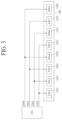
- the display panel 110 includes eight channels
- the third array 240 is composed of eight holding latches 310 - 1 to 310 - 8
- the latch groups include a first latch group LG 1 , a second latch group LG 2 , a third latch group LG 3 , and a fourth latch group LG 4 .
- the first latch group LG 1 is composed of the holding latches 310 - 1 and 310 - 5 which latch image data of a red sub-pixel
- the second latch group LG 2 is composed of the holding latches 310 - 2 and 310 - 6 which latch image data of a first green sub-pixel.
- the third latch group LG 3 is composed of the holding latches 310 - 3 and 310 - 7 which latch image data of a blue sub-pixel
- the fourth latch group LG 4 is composed of the holding latches 310 - 4 and 310 - 8 which latch image data of a second green sub-pixel.
- the signal generation circuit 230 generates a first latch enable signal EN 1 for the first latch group LG 1 and applies the first latch enable signal EN 1 to the holding latches 310 - 1 and 310 - 5 of the first latch group LG 1 , and generates a second latch enable signal EN 2 for the second latch group LG 2 and applies the second latch enable signal EN 2 to the holding latches 310 - 2 and 310 - 6 of the second latch group LG 2 .
- the signal generation circuit 230 generates a third latch enable signal EN 3 for the third latch group LG 3 and applies the third latch enable signal EN 3 to the holding latches 310 - 3 and 310 - 7 of the third latch group LG 3 , and generates a fourth latch enable signal EN 4 for the fourth latch group LG 4 and applies the fourth latch enable signal EN 4 to the holding latches 310 - 4 and 310 - 8 of the fourth latch group LG 4 .
- the first to fourth latch groups LG 1 to LG 4 may perform the latch operation at different latch timings, and the holding latches included in the same latch group may simultaneously perform the latch operation.
- the signal generation circuit 230 may cause the holding latches of each latch group to latch the image data output from the sampling latches during a section in which the latch enable signal is at a high level, and may cause the holding latches to latch the image data at different timings for the latch groups by generating latch enable signals so that high-level sections of the latch enable signals for each latch group do not overlap each other.
- the signal generation circuit 230 may generate the latch enable signals for each latch group so that the latch enable signal for each latch group transitions from a low level to a high level when a first number of clock pulses is counted from a rising edge of a horizontal synchronization signal Hsync which indicates a start of one horizontal line, and transitions from the high level to the low level when a second number of clock pulses is counted from the rising edge.
- the first number of clock pulses and the second number of clock pulses are set differently for each latch group.
- the signal generation circuit 230 since the signal generation circuit 230 generates the latch enable signals using a number of clock pulses counted based on the rising edge of the horizontal synchronization signal Hsync, and thus the latch enable signals may be generated in a digital manner, accuracy of the latch enable signals may be improved compared to a method of generating the latch enable signals in an analog manner using a delay circuit or the like.
- information which indicates a latch timing at which the image data for each channel for each latch group is latched may be stored in a register 232 , and the signal generation circuit 230 may generate the latch enable signal of each latch group based on the latch timing for each latch group stored in the register 232 .
- the latch timing at which the image data for each channel is latched may be defined as the number of clock pulse signals.
- the signal generation circuit 230 when four latch groups are formed for each color, the signal generation circuit 230 generates the second latch enable signal EN 2 for the second latch group LG 2 .
- the second latch enable signal EN 2 may transition from the low level to the high level at the same timing as a rising edge RE 1 of the horizontal synchronization signal Hsync which indicates the start of one horizontal line (a time at which a first clock signal is counted), and may transition from the high level to the low level at a time at which a second clock signal is counted from the rising edge RE 1 of the horizontal synchronization signal Hsync.
- the signal generation circuit 230 generates the fourth latch enable signal EN 4 for the fourth latch group LG 4 .
- the fourth latch enable signal EN 4 may transition from the low level to the high level at the time at which the second clock signal is counted from the rising edge RE 1 of the horizontal synchronization signal Hsync, and may transition from the high level to the low level at a time at which a third clock signal is counted from the rising edge RE 1 of the horizontal synchronization signal Hsync.
- the signal generation circuit 230 generates the first latch enable signal EN 1 for the first latch group LG 1 .
- the first latch enable signal EN 1 may transition from the low level to the high level at the time at which the third clock signal is counted from the rising edge RE 1 of the horizontal synchronization signal Hsync, and may transition from the high level to the low level at a time at which a fourth clock signal is counted from the rising edge RE 1 of the horizontal synchronization signal Hsync.
- the signal generation circuit 230 generates the third latch enable signal EN 3 for the third latch group LG 3 .
- the third latch enable signal EN 3 may transition from the low level to the high level at the time at which the fourth clock signal is counted from the rising edge RE 1 of the horizontal synchronization signal Hsync, and may transition from the high level to the low level at a time at which a fifth clock signal is counted from the rising edge RE 1 of the horizontal synchronization signal Hsync.
- the signal generation circuit 230 may generate latch enable signals of which high-level sections do not overlap each other for each latch group, and the holding latches may operate at different timings for the latch groups according to the latch enable signals generated for each latch group.
- the level shifters 250 a to 250 m included in the level shifter array 250 changes a voltage level of the image data for the channels latched in the holding latches 240 a to 240 m to a predetermined voltage level.
- the level shifters 250 a to 250 m operate at the same timing as the holding latches 240 a to 240 m , respectively, the level shifters 250 a to 250 m also operate at the different timings for the colors of the image data for the channels. Accordingly, since a current concentration phenomenon which occurs as all of the level shifters 250 a to 250 m operate at the same time may be prevented, the generation of power noise due to the current concentration phenomenon may be prevented.
- the digital-to-analog converters 260 a to 260 m included in the fourth array 260 convert the image data for each channel of which a voltage level is shifted using a gray scale voltage generated by the gamma voltage generation circuit 270 to a data signal (data voltage) in an analog form.
- the gamma voltage generation circuit 270 generates a plurality of gray scale voltages V 0 to V 255 for outputting the image data for each channel using a resistor string, and supplies the generated gray scale voltages to the digital-to-analog converters 260 a to 260 m.
- the output buffers 280 a to 280 m included in the fifth array 280 amplify the data signals for the channels output from the digital-to-analog converters 260 a to 260 m to output the data signals to the pixels P of the display panel through the data lines DL respectively corresponding to the channels.
- the image data for each channel is composed of 6 bits and the holding latches, which latch the first and second green image data, latch the image data before the holding latches, which latch the red and blue image data, will be described.
- the second and sixth holding latches 310 - 2 and 310 - 6 latch the first green image data G 1 output from the corresponding sampling latches (not shown) during a section in which the second latch enable signal EN 2 is at a high level.
- the fourth and eighth holding latches 310 - 4 and 310 - 8 latch the second green image data G 2 output from the corresponding sampling latches (not shown) during a section in which the fourth latch enable signal EN 4 is at a high level.
- the first and fifth holding latches 310 - 1 and 310 - 5 latch the red image data R output from the corresponding sampling latches during a section in which the first latch enable signal EN 1 is at a high level.
- the third and seventh holding latches 310 - 3 and 310 - 7 latch the blue image data B output from the corresponding sampling latches during a section in which the third latch enable signal EN 3 is at a high level.
- the holding latches 310 - 1 to 310 - 8 included in the latch groups LG 1 to LG 4 latch the image data for the channels at different latch timings according to the latch enable signals EN 1 to EN 4 respectively generated for the latch groups LG 1 to LG 4 , it can be seen that the data latch timings are dispersed between the holding latches 310 - 1 to 310 - 8 .
- the holding latches 240 a to 240 m latch the image data for the channels at different latch timings for the latch groups each composed of the plurality of holding latches 240 a to 240 m .
- the holding latches 240 a to 240 m may latch the image data for the channels at different timings for each predetermined cell group.
- a configuration of the data driver 124 according to the second embodiment is the same as the configuration shown in FIG. 2 , and functions of the shift registers 210 a to 210 m , the sampling latches 220 a to 220 m , the digital-to-analog converters 260 a to 260 m , the gamma voltage generation circuit 270 , and the output buffers 280 a to 280 m according to the second embodiment are the same as those shown in the first embodiment, hereinafter, the second embodiment will be described mainly with functions of the signal generation circuit 230 , the holding latches 240 a to 240 m , and the level shifters 250 a to 250 m.
- the holding latches 240 a to 240 m latch bits of pieces of image data for channels output from the sampling latches 220 a to 220 m at different timings according to latch enable signals generated for each predetermined cell group.
- the cell group may be composed of latch cells having the same position in each of the holding latches 240 a to 240 m .
- first latch cells in which the most significant bits (MSBs) are latched may be set as a first cell group
- second latch cells in which second bits are latched in the holding latches 240 a to 240 m may be set as a second cell group
- nth latch cells in which least significant bits (LSBs) are latched in the holding latches 240 a to 240 m may be set as an nth cell group.
- the latch cells included in the first cell group, the latch cells included in the second cell group, and the latch cells included in the nth cell group latch the bits of the image data output from the sampling latches 220 a to 220 m at different latch timings.
- the latch cells included in the first cell group simultaneously latch the most significant bits, which are the first bits of the pieces of image data at a first latch timing
- the latch cells included in the second cell group simultaneously latch the second bits of the pieces of image data at a second latch timing
- the latch cells included in the nth cell group simultaneously latch the least significant bits, which are the last bits of the pieces of image data at an nth latch timing.
- the bits of the image data for the channels are latched in the holding latches 240 a to 240 m at different latch timings set for the latch cells, current concentration which occurs due to simultaneous change of all bits when the image data is changed may be prevented, and accordingly, power noise may be dispersed and EMI may also be decreased.
- the bits of the pieces of image data may be sequentially latched in the holding latches 240 a to 240 m in an order from the first cell group composed of the latch cells in which the most significant bits are latched to the nth cell group composed of the latch cells in which the least significant bits are latched. This is to prevent the user's eyes from recognizing an image difference which may occur due to dispersion of a change time of the bits constituting the image data by changing the most significant bits first.
- each cell group includes one latch cell for each holding latch 240 a to 240 m , but in another embodiment, two or more latch cells for each holding latch 240 a to 240 m may be included in one cell group.
- the data driver 124 includes m holding latches 240 a to 240 m , and two latch cells are included for each holding latch in one cell group, n/2 cell groups may be generated, and each cell group may be composed of 2 ⁇ m latch cells.
- the signal generation circuit 230 generates the latch enable signal for enabling an operation of the holding latches 240 a to 240 m for each cell group. For example, when n cell groups are formed, since the signal generation circuit 230 may generate one latch enable signal for each cell group, a total of n latch enable signals may be generated.
- the display panel 110 includes eight channels
- the third array 240 is composed of eight holding latches 310 - 1 to 310 - 8
- the image data for each channel is composed of six bits
- each of the holding latches 310 - 1 to 310 - 8 includes six latch cells and six cell groups SG 1 to SG 6 are formed by grouping the latch cells at the same positions.
- the signal generation circuit 230 generates a first latch enable signal EN 1 for a first cell group SG 1 and applies the first latch enable signal EN 1 to latch cells a 1 to a 8 of the first cell group SG 1 , generates a second latch enable signal EN 2 for a second cell group SG 2 and applies the second latch enable signal EN 2 to latch cells b 1 to b 8 of the second cell group SG 2 , generates a third latch enable signal EN 3 for a third cell group SG 3 and applies the third latch enable signal EN 3 to latch cells c 1 to c 8 of the third cell group SG 3 , generates a fourth latch enable signal EN 4 for a fourth cell group SG 4 and applies the fourth latch enable signal EN 4 to latch cells d 1 to d 8 of the fourth cell group SG 4 , generates a fifth latch enable signal EN 5 for a fifth cell group SG 5 and applies the fifth latch enable signal EN 5 to latch cells e 1 to e 8 of the fifth cell group SG 5 , and generates a sixth latch enable
- the first to sixth cell groups SG 1 to SG 6 may perform a latch operation at different latch timings, and the latch cells included in the same cell group may simultaneously perform the latch operation.
- the signal generation circuit 230 may generate the latch enable signals so that the latch cells of the holding latches 240 a to 240 m may latch the bits output from the sampling latches 220 a to 220 m at a latch timing designated for each cell group during a section in which the latch enable signals of each cell group are at a high level.
- the signal generation circuit 230 may cause the latch cells of the holding latches 240 a to 240 m to latch the bits of the image data at different latch timings for the cell groups by generating latch enable signals so that high-level sections of the latch enable signals of each cell group do not overlap each other.
- the signal generation circuit 230 may generate the latch enable signals for each cell group to transition from a low level to a high level when a first number of clock pulses is counted from a rising edge of a horizontal synchronization signal Hsync which indicates a start of one horizontal line, and transition from the high level to the low level when a second number of clock pulses is counted from the rising edge.
- the first number of clock pulses and the second number of clock pulses may be set differently for each cell group.
- information about a latch timing at which the bits of the image data for each cell group are latched may be stored in the register 232 , and the signal generation circuit 230 may generate the latch enable signals of each cell group based on the latch timing for each cell group stored in the register 232 .
- the latch timing may be defined as the number of clock pulse signals of CLK.
- the signal generation circuit 230 may generate latch enable signals of which the high-level sections do not overlap each other for each cell group, and the latch cells of the holding latches 240 a to 240 m latch the bits of the image data for each channel at different latch timings according to the latch enable signals generated for the cell groups.
- the level shifters 250 a to 250 m changes a voltage level of the bit latched in each latch cell to a predetermined voltage level.
- the level shifters 250 a to 250 m operate at the same timing as the holding latches 240 a to 240 m , respectively, the level shifters 250 a to 250 m also operate at different timings for each cell group. Accordingly, since a current concentration phenomenon which occurs as all of the level shifters 250 a to 250 m operate at the same time may be prevented, the generation of power noise due to the current concentration phenomenon may be prevented.
- the display panel 110 includes eight channels, and the bits are sequentially latched in an order from the first cell group SG 1 composed of the latch cells which latch the most significant bits to the sixth cell group SG 6 composed of the latch cells which latch the least significant bits will be described.
- Eight sampling latches sequentially sample and latch the image data for each channel in units of bits based on source start pulses input from shift registers (not shown).
- the first latch enable signal EN 1 for the first cell group SG 1 composed of the first latch cells a 1 to a 8 which latch the most significant bits D 1 that are first bits of the pieces of image data for the channels is applied to the eight holding latches 310 - 1 to 310 - 8 from the signal generation circuit 230
- the first latch cells a 1 to a 8 included in the eight holding latches 310 - 1 to 310 - 8 latch the most significant bits D 1 output from the sampling latches during a section in which the first latch enable signal EN 1 is at the high level.
- the second latch enable signal EN 2 for the second cell group SG 2 composed of the second latch cells b 1 to b 8 which latch second bits D 2 is applied to the eight holding latches 310 - 1 to 310 - 8 from the signal generation circuit 230
- the second latch cells b 1 to b 8 included in the eight holding latches 310 - 1 to 310 - 8 latch the second bits D 2 output from the sampling latches during a section in which the second latch enable signal EN 2 is at the high level.
- the latch cells of the holding latches 310 - 1 to 310 - 8 latch the bits of the image data at different latch timing according to the latch enable signals EN 1 to EN 6 generated for each cell group, it can be seen that the latch timings are dispersed in units of bits.
- a latch timing at which bits of image data latched in sampling latches are latched in holding latches can be set differently for each color or bit, there is an effect in that a current concentration phenomenon which occurs as the bits of the image data are simultaneously changed can be prevented, and accordingly, power noise can be dispersed.
- a latch timing at which bits of image data latched in sampling latches are latched in holding latches can be set differently for each color or bit, there is an effect in that a time at which a load of a gamma voltage generation circuit which serves as a reference of the source driver IC is changed can be distributed, and thus a settling time becomes quicker.
- All disclosed methods and procedures described herein may be implemented, at least in part, using one or more computer programs or components. These components may be provided as a series of computer instructions through any conventional computer-readable medium or machine-readable medium including volatile and nonvolatile memories such as random-access memories (RAMs), read only-memories (ROMs), flash memories, magnetic or optical disks, optical memories, or other storage media.
- RAMs random-access memories
- ROMs read only-memories
- flash memories magnetic or optical disks
- optical memories optical memories
- the instructions may be provided as software or firmware, and may, in whole or in part, be implemented in a hardware configuration such as application-specific integrated circuits (ASICs), field-programmable gate arrays (FPGAs), digital signal processors (DSPs), or any other similar device.
- ASICs application-specific integrated circuits
- FPGAs field-programmable gate arrays
- DSPs digital signal processors
- the instructions may be configured to be executed by one or more processors or other hardware configurations, and the processor
Landscapes
- Engineering & Computer Science (AREA)
- Physics & Mathematics (AREA)
- Computer Hardware Design (AREA)
- General Physics & Mathematics (AREA)
- Theoretical Computer Science (AREA)
- Chemical & Material Sciences (AREA)
- Crystallography & Structural Chemistry (AREA)
- Multimedia (AREA)
- Control Of Indicators Other Than Cathode Ray Tubes (AREA)
- Liquid Crystal Display Device Control (AREA)
- Control Of El Displays (AREA)
Abstract
Description
Claims (17)
Applications Claiming Priority (2)
| Application Number | Priority Date | Filing Date | Title |
|---|---|---|---|
| KR10-2021-0187929 | 2021-12-27 | ||
| KR1020210187929A KR102897242B1 (en) | 2021-12-27 | 2021-12-27 | Device and Method for Driving Display |
Publications (2)
| Publication Number | Publication Date |
|---|---|
| US20230206883A1 US20230206883A1 (en) | 2023-06-29 |
| US12190850B2 true US12190850B2 (en) | 2025-01-07 |
Family
ID=86897044
Family Applications (1)
| Application Number | Title | Priority Date | Filing Date |
|---|---|---|---|
| US18/073,092 Active 2042-12-01 US12190850B2 (en) | 2021-12-27 | 2022-12-01 | Display driving device and method of driving display system |
Country Status (4)
| Country | Link |
|---|---|
| US (1) | US12190850B2 (en) |
| KR (1) | KR102897242B1 (en) |
| CN (1) | CN116403500A (en) |
| TW (1) | TW202326655A (en) |
Families Citing this family (1)
| Publication number | Priority date | Publication date | Assignee | Title |
|---|---|---|---|---|
| CN119851595A (en) * | 2025-02-26 | 2025-04-18 | 北京奕斯伟计算技术股份有限公司 | Source electrode driving circuit, source electrode driving chip and display driving method |
Citations (3)
| Publication number | Priority date | Publication date | Assignee | Title |
|---|---|---|---|---|
| US20080001944A1 (en) * | 2006-06-30 | 2008-01-03 | Himax Technologies Limited | Low power lcd source driver |
| US20190304395A1 (en) * | 2018-03-30 | 2019-10-03 | Samsung Electronics Co., Ltd. | Source driver and display driver including the same |
| US20230282150A1 (en) * | 2020-11-23 | 2023-09-07 | Snap Inc. | System and method for driving a pixel with optimized power and area |
Family Cites Families (2)
| Publication number | Priority date | Publication date | Assignee | Title |
|---|---|---|---|---|
| KR20120092810A (en) * | 2011-02-14 | 2012-08-22 | 삼성전자주식회사 | Source driver, display device including the same, and method for driving the display device |
| KR102771258B1 (en) * | 2020-04-28 | 2025-02-25 | 삼성디스플레이 주식회사 | Data driver and display device a data driver |
-
2021
- 2021-12-27 KR KR1020210187929A patent/KR102897242B1/en active Active
-
2022
- 2022-11-23 TW TW111144862A patent/TW202326655A/en unknown
- 2022-11-24 CN CN202211480894.XA patent/CN116403500A/en active Pending
- 2022-12-01 US US18/073,092 patent/US12190850B2/en active Active
Patent Citations (3)
| Publication number | Priority date | Publication date | Assignee | Title |
|---|---|---|---|---|
| US20080001944A1 (en) * | 2006-06-30 | 2008-01-03 | Himax Technologies Limited | Low power lcd source driver |
| US20190304395A1 (en) * | 2018-03-30 | 2019-10-03 | Samsung Electronics Co., Ltd. | Source driver and display driver including the same |
| US20230282150A1 (en) * | 2020-11-23 | 2023-09-07 | Snap Inc. | System and method for driving a pixel with optimized power and area |
Also Published As
| Publication number | Publication date |
|---|---|
| KR102897242B1 (en) | 2025-12-08 |
| TW202326655A (en) | 2023-07-01 |
| CN116403500A (en) | 2023-07-07 |
| US20230206883A1 (en) | 2023-06-29 |
| KR20230098941A (en) | 2023-07-04 |
Similar Documents
| Publication | Publication Date | Title |
|---|---|---|
| CN111179798B (en) | Display device and driving method thereof | |
| US10783848B2 (en) | Display device subpixel activation patterns | |
| US11482150B2 (en) | Device and method for driving display supporting low power mode | |
| CN101051448B (en) | Semiconductor integrated circuit device used in data line driver of plane type display apparatus | |
| US11132978B2 (en) | Gamma correction circuit, method for gamma correction, and display device including gamma correction circuit | |
| CN112216239B (en) | Source driver and display device | |
| US11847979B2 (en) | Display apparatus and driving method thereof | |
| CN112669745A (en) | Scan driver and display device having the same | |
| US12322356B2 (en) | Source driver integrated circuit and method for driving the same | |
| US12190850B2 (en) | Display driving device and method of driving display system | |
| US12033582B2 (en) | Level shifter and display device including the same | |
| US11798466B2 (en) | Data driving unit and display device including the same | |
| US20250209991A1 (en) | Scan Signal Generation Circuit and Display Device Including the Same | |
| US7616183B2 (en) | Source driving circuit of display device and source driving method thereof | |
| US20080030444A1 (en) | Gamma voltage generator, source driver, and display device utilizing the same | |
| KR20230103567A (en) | Special-shaped display panel and special-shaped display device using the same | |
| US20250209952A1 (en) | Gamma voltage generation circuit and display device including the same | |
| US11574604B2 (en) | Display device and method for driving the same | |
| US20260057826A1 (en) | Gamma voltage generating circuit and display device including the same | |
| KR20260023179A (en) | Level shifter and display device including the same | |
| KR20160083377A (en) | Data Driver And Display Device Including The Same | |
| KR20240128776A (en) | Data driving circuit, display device including the same, and method for driving the same | |
| CN120412461A (en) | Display device and driving method thereof | |
| CN120236532A (en) | Display panel and display device including the same |
Legal Events
| Date | Code | Title | Description |
|---|---|---|---|
| AS | Assignment |
Owner name: LX SEMICON CO., LTD., KOREA, REPUBLIC OF Free format text: ASSIGNMENT OF ASSIGNORS INTEREST;ASSIGNORS:JEONG, BYEONG HO;KIM, SUNG HA;REEL/FRAME:061945/0364 Effective date: 20221122 |
|
| FEPP | Fee payment procedure |
Free format text: ENTITY STATUS SET TO UNDISCOUNTED (ORIGINAL EVENT CODE: BIG.); ENTITY STATUS OF PATENT OWNER: LARGE ENTITY |
|
| STPP | Information on status: patent application and granting procedure in general |
Free format text: DOCKETED NEW CASE - READY FOR EXAMINATION |
|
| STPP | Information on status: patent application and granting procedure in general |
Free format text: NON FINAL ACTION MAILED |
|
| STPP | Information on status: patent application and granting procedure in general |
Free format text: RESPONSE TO NON-FINAL OFFICE ACTION ENTERED AND FORWARDED TO EXAMINER |
|
| STPP | Information on status: patent application and granting procedure in general |
Free format text: FINAL REJECTION MAILED |
|
| STPP | Information on status: patent application and granting procedure in general |
Free format text: NOTICE OF ALLOWANCE MAILED -- APPLICATION RECEIVED IN OFFICE OF PUBLICATIONS |
|
| STPP | Information on status: patent application and granting procedure in general |
Free format text: PUBLICATIONS -- ISSUE FEE PAYMENT VERIFIED |
|
| STCF | Information on status: patent grant |
Free format text: PATENTED CASE |