US12190822B2 - Array substrate and display apparatus - Google Patents
Array substrate and display apparatus Download PDFInfo
- Publication number
- US12190822B2 US12190822B2 US18/255,100 US202218255100A US12190822B2 US 12190822 B2 US12190822 B2 US 12190822B2 US 202218255100 A US202218255100 A US 202218255100A US 12190822 B2 US12190822 B2 US 12190822B2
- Authority
- US
- United States
- Prior art keywords
- pad
- columns
- array substrate
- layer
- pixel driving
- Prior art date
- Legal status (The legal status is an assumption and is not a legal conclusion. Google has not performed a legal analysis and makes no representation as to the accuracy of the status listed.)
- Active
Links
Images


Classifications
-
- G—PHYSICS
- G09—EDUCATION; CRYPTOGRAPHY; DISPLAY; ADVERTISING; SEALS
- G09G—ARRANGEMENTS OR CIRCUITS FOR CONTROL OF INDICATING DEVICES USING STATIC MEANS TO PRESENT VARIABLE INFORMATION
- G09G3/00—Control arrangements or circuits, of interest only in connection with visual indicators other than cathode-ray tubes
- G09G3/20—Control arrangements or circuits, of interest only in connection with visual indicators other than cathode-ray tubes for presentation of an assembly of a number of characters, e.g. a page, by composing the assembly by combination of individual elements arranged in a matrix no fixed position being assigned to or needed to be assigned to the individual characters or partial characters
- G09G3/22—Control arrangements or circuits, of interest only in connection with visual indicators other than cathode-ray tubes for presentation of an assembly of a number of characters, e.g. a page, by composing the assembly by combination of individual elements arranged in a matrix no fixed position being assigned to or needed to be assigned to the individual characters or partial characters using controlled light sources
- G09G3/30—Control arrangements or circuits, of interest only in connection with visual indicators other than cathode-ray tubes for presentation of an assembly of a number of characters, e.g. a page, by composing the assembly by combination of individual elements arranged in a matrix no fixed position being assigned to or needed to be assigned to the individual characters or partial characters using controlled light sources using electroluminescent panels
- G09G3/32—Control arrangements or circuits, of interest only in connection with visual indicators other than cathode-ray tubes for presentation of an assembly of a number of characters, e.g. a page, by composing the assembly by combination of individual elements arranged in a matrix no fixed position being assigned to or needed to be assigned to the individual characters or partial characters using controlled light sources using electroluminescent panels semiconductive, e.g. using light-emitting diodes [LED]
- G09G3/3208—Control arrangements or circuits, of interest only in connection with visual indicators other than cathode-ray tubes for presentation of an assembly of a number of characters, e.g. a page, by composing the assembly by combination of individual elements arranged in a matrix no fixed position being assigned to or needed to be assigned to the individual characters or partial characters using controlled light sources using electroluminescent panels semiconductive, e.g. using light-emitting diodes [LED] organic, e.g. using organic light-emitting diodes [OLED]
- G09G3/3225—Control arrangements or circuits, of interest only in connection with visual indicators other than cathode-ray tubes for presentation of an assembly of a number of characters, e.g. a page, by composing the assembly by combination of individual elements arranged in a matrix no fixed position being assigned to or needed to be assigned to the individual characters or partial characters using controlled light sources using electroluminescent panels semiconductive, e.g. using light-emitting diodes [LED] organic, e.g. using organic light-emitting diodes [OLED] using an active matrix
- G09G3/3258—Control arrangements or circuits, of interest only in connection with visual indicators other than cathode-ray tubes for presentation of an assembly of a number of characters, e.g. a page, by composing the assembly by combination of individual elements arranged in a matrix no fixed position being assigned to or needed to be assigned to the individual characters or partial characters using controlled light sources using electroluminescent panels semiconductive, e.g. using light-emitting diodes [LED] organic, e.g. using organic light-emitting diodes [OLED] using an active matrix with pixel circuitry controlling the voltage across the light-emitting element
-
- H—ELECTRICITY
- H10—SEMICONDUCTOR DEVICES; ELECTRIC SOLID-STATE DEVICES NOT OTHERWISE PROVIDED FOR
- H10K—ORGANIC ELECTRIC SOLID-STATE DEVICES
- H10K59/00—Integrated devices, or assemblies of multiple devices, comprising at least one organic light-emitting element covered by group H10K50/00
- H10K59/10—OLED displays
- H10K59/12—Active-matrix OLED [AMOLED] displays
- H10K59/131—Interconnections, e.g. wiring lines or terminals
-
- G—PHYSICS
- G09—EDUCATION; CRYPTOGRAPHY; DISPLAY; ADVERTISING; SEALS
- G09G—ARRANGEMENTS OR CIRCUITS FOR CONTROL OF INDICATING DEVICES USING STATIC MEANS TO PRESENT VARIABLE INFORMATION
- G09G2300/00—Aspects of the constitution of display devices
- G09G2300/04—Structural and physical details of display devices
- G09G2300/0421—Structural details of the set of electrodes
- G09G2300/0426—Layout of electrodes and connections
-
- G—PHYSICS
- G09—EDUCATION; CRYPTOGRAPHY; DISPLAY; ADVERTISING; SEALS
- G09G—ARRANGEMENTS OR CIRCUITS FOR CONTROL OF INDICATING DEVICES USING STATIC MEANS TO PRESENT VARIABLE INFORMATION
- G09G2300/00—Aspects of the constitution of display devices
- G09G2300/08—Active matrix structure, i.e. with use of active elements, inclusive of non-linear two terminal elements, in the pixels together with light emitting or modulating elements
- G09G2300/0809—Several active elements per pixel in active matrix panels
- G09G2300/0819—Several active elements per pixel in active matrix panels used for counteracting undesired variations, e.g. feedback or autozeroing
-
- G—PHYSICS
- G09—EDUCATION; CRYPTOGRAPHY; DISPLAY; ADVERTISING; SEALS
- G09G—ARRANGEMENTS OR CIRCUITS FOR CONTROL OF INDICATING DEVICES USING STATIC MEANS TO PRESENT VARIABLE INFORMATION
- G09G2300/00—Aspects of the constitution of display devices
- G09G2300/08—Active matrix structure, i.e. with use of active elements, inclusive of non-linear two terminal elements, in the pixels together with light emitting or modulating elements
- G09G2300/0809—Several active elements per pixel in active matrix panels
- G09G2300/0842—Several active elements per pixel in active matrix panels forming a memory circuit, e.g. a dynamic memory with one capacitor
- G09G2300/0852—Several active elements per pixel in active matrix panels forming a memory circuit, e.g. a dynamic memory with one capacitor being a dynamic memory with more than one capacitor
-
- G—PHYSICS
- G09—EDUCATION; CRYPTOGRAPHY; DISPLAY; ADVERTISING; SEALS
- G09G—ARRANGEMENTS OR CIRCUITS FOR CONTROL OF INDICATING DEVICES USING STATIC MEANS TO PRESENT VARIABLE INFORMATION
- G09G2300/00—Aspects of the constitution of display devices
- G09G2300/08—Active matrix structure, i.e. with use of active elements, inclusive of non-linear two terminal elements, in the pixels together with light emitting or modulating elements
- G09G2300/0809—Several active elements per pixel in active matrix panels
- G09G2300/0842—Several active elements per pixel in active matrix panels forming a memory circuit, e.g. a dynamic memory with one capacitor
- G09G2300/0861—Several active elements per pixel in active matrix panels forming a memory circuit, e.g. a dynamic memory with one capacitor with additional control of the display period without amending the charge stored in a pixel memory, e.g. by means of additional select electrodes
-
- G—PHYSICS
- G09—EDUCATION; CRYPTOGRAPHY; DISPLAY; ADVERTISING; SEALS
- G09G—ARRANGEMENTS OR CIRCUITS FOR CONTROL OF INDICATING DEVICES USING STATIC MEANS TO PRESENT VARIABLE INFORMATION
- G09G2310/00—Command of the display device
- G09G2310/02—Addressing, scanning or driving the display screen or processing steps related thereto
- G09G2310/0243—Details of the generation of driving signals
- G09G2310/0251—Precharge or discharge of pixel before applying new pixel voltage
-
- G—PHYSICS
- G09—EDUCATION; CRYPTOGRAPHY; DISPLAY; ADVERTISING; SEALS
- G09G—ARRANGEMENTS OR CIRCUITS FOR CONTROL OF INDICATING DEVICES USING STATIC MEANS TO PRESENT VARIABLE INFORMATION
- G09G2320/00—Control of display operating conditions
- G09G2320/02—Improving the quality of display appearance
- G09G2320/0209—Crosstalk reduction, i.e. to reduce direct or indirect influences of signals directed to a certain pixel of the displayed image on other pixels of said image, inclusive of influences affecting pixels in different frames or fields or sub-images which constitute a same image, e.g. left and right images of a stereoscopic display
-
- G—PHYSICS
- G09—EDUCATION; CRYPTOGRAPHY; DISPLAY; ADVERTISING; SEALS
- G09G—ARRANGEMENTS OR CIRCUITS FOR CONTROL OF INDICATING DEVICES USING STATIC MEANS TO PRESENT VARIABLE INFORMATION
- G09G2320/00—Control of display operating conditions
- G09G2320/02—Improving the quality of display appearance
- G09G2320/0242—Compensation of deficiencies in the appearance of colours
-
- G—PHYSICS
- G09—EDUCATION; CRYPTOGRAPHY; DISPLAY; ADVERTISING; SEALS
- G09G—ARRANGEMENTS OR CIRCUITS FOR CONTROL OF INDICATING DEVICES USING STATIC MEANS TO PRESENT VARIABLE INFORMATION
- G09G3/00—Control arrangements or circuits, of interest only in connection with visual indicators other than cathode-ray tubes
- G09G3/20—Control arrangements or circuits, of interest only in connection with visual indicators other than cathode-ray tubes for presentation of an assembly of a number of characters, e.g. a page, by composing the assembly by combination of individual elements arranged in a matrix no fixed position being assigned to or needed to be assigned to the individual characters or partial characters
- G09G3/22—Control arrangements or circuits, of interest only in connection with visual indicators other than cathode-ray tubes for presentation of an assembly of a number of characters, e.g. a page, by composing the assembly by combination of individual elements arranged in a matrix no fixed position being assigned to or needed to be assigned to the individual characters or partial characters using controlled light sources
- G09G3/30—Control arrangements or circuits, of interest only in connection with visual indicators other than cathode-ray tubes for presentation of an assembly of a number of characters, e.g. a page, by composing the assembly by combination of individual elements arranged in a matrix no fixed position being assigned to or needed to be assigned to the individual characters or partial characters using controlled light sources using electroluminescent panels
- G09G3/32—Control arrangements or circuits, of interest only in connection with visual indicators other than cathode-ray tubes for presentation of an assembly of a number of characters, e.g. a page, by composing the assembly by combination of individual elements arranged in a matrix no fixed position being assigned to or needed to be assigned to the individual characters or partial characters using controlled light sources using electroluminescent panels semiconductive, e.g. using light-emitting diodes [LED]
- G09G3/3208—Control arrangements or circuits, of interest only in connection with visual indicators other than cathode-ray tubes for presentation of an assembly of a number of characters, e.g. a page, by composing the assembly by combination of individual elements arranged in a matrix no fixed position being assigned to or needed to be assigned to the individual characters or partial characters using controlled light sources using electroluminescent panels semiconductive, e.g. using light-emitting diodes [LED] organic, e.g. using organic light-emitting diodes [OLED]
- G09G3/3225—Control arrangements or circuits, of interest only in connection with visual indicators other than cathode-ray tubes for presentation of an assembly of a number of characters, e.g. a page, by composing the assembly by combination of individual elements arranged in a matrix no fixed position being assigned to or needed to be assigned to the individual characters or partial characters using controlled light sources using electroluminescent panels semiconductive, e.g. using light-emitting diodes [LED] organic, e.g. using organic light-emitting diodes [OLED] using an active matrix
- G09G3/3233—Control arrangements or circuits, of interest only in connection with visual indicators other than cathode-ray tubes for presentation of an assembly of a number of characters, e.g. a page, by composing the assembly by combination of individual elements arranged in a matrix no fixed position being assigned to or needed to be assigned to the individual characters or partial characters using controlled light sources using electroluminescent panels semiconductive, e.g. using light-emitting diodes [LED] organic, e.g. using organic light-emitting diodes [OLED] using an active matrix with pixel circuitry controlling the current through the light-emitting element
-
- H—ELECTRICITY
- H10—SEMICONDUCTOR DEVICES; ELECTRIC SOLID-STATE DEVICES NOT OTHERWISE PROVIDED FOR
- H10K—ORGANIC ELECTRIC SOLID-STATE DEVICES
- H10K59/00—Integrated devices, or assemblies of multiple devices, comprising at least one organic light-emitting element covered by group H10K50/00
- H10K59/10—OLED displays
- H10K59/12—Active-matrix OLED [AMOLED] displays
- H10K59/121—Active-matrix OLED [AMOLED] displays characterised by the geometry or disposition of pixel elements
- H10K59/1213—Active-matrix OLED [AMOLED] displays characterised by the geometry or disposition of pixel elements the pixel elements being TFTs
-
- H—ELECTRICITY
- H10—SEMICONDUCTOR DEVICES; ELECTRIC SOLID-STATE DEVICES NOT OTHERWISE PROVIDED FOR
- H10K—ORGANIC ELECTRIC SOLID-STATE DEVICES
- H10K59/00—Integrated devices, or assemblies of multiple devices, comprising at least one organic light-emitting element covered by group H10K50/00
- H10K59/10—OLED displays
- H10K59/12—Active-matrix OLED [AMOLED] displays
- H10K59/121—Active-matrix OLED [AMOLED] displays characterised by the geometry or disposition of pixel elements
- H10K59/1216—Active-matrix OLED [AMOLED] displays characterised by the geometry or disposition of pixel elements the pixel elements being capacitors
Definitions
- the present invention relates to display technology, more particularly, to an array substrate and a display apparatus.
- OLED display is one of the hotspots in the field of flat panel display research today. Unlike Thin Film Transistor-Liquid Crystal Display (TFT-LCD), which uses a stable voltage to control brightness, OLED is driven by a driving current required to be kept constant to control illumination.
- the OLED display panel includes a plurality of pixel units configured with pixel-driving circuits arranged in multiple rows and columns. Each pixel-driving circuit includes a driving transistor having a gate terminal connected to one gate line per row and a drain terminal connected to one data line per column.
- the switching transistor connected to the driving transistor is turned on, and the data voltage is applied from the data line to the driving transistor via the switching transistor, so that the driving transistor outputs a current corresponding to the data voltage to an OLED device.
- the OLED device is driven to emit light of a corresponding brightness.
- the present disclosure provides an array substrate, comprising K number of columns of first pads; wherein a respective first pad is connected to an anode of a light emitting element, a second electrode of a fifth transistor, and a second electrode of a sixth transistor; the K number of columns of first pads comprise a plurality of first-first pads in (2k-1)-th columns of the K columns and a plurality of second-first pads in (2k)-th columns of the K columns; and a respective first-first pad and a respective second-first pad have different average line widths.
- the array substrate further comprises multiple first-first reset signal lines in the (2k-1)-th columns and multiple second-first reset signal lines in the (2k)-th columns of the K columns; wherein a first parasitic capacitance between a respective first-first pad and a respective first-first reset signal line in the (2k-1)-th columns of the K columns is different from a second parasitic capacitance between a respective second-first pad and a respective second-first reset signal line in the (2k)-th columns of the K columns.
- the first parasitic capacitance is greater than the second parasitic capacitance by at least 5%.
- orthographic projections of the respective first-first pad and the respective first-first reset signal line in the (2k-1)-th columns of the K columns overlap with each other in a first overlapping region having a first area; orthographic projections of the respective second-first pad and the respective second-first reset signal line in the (2k)-th columns of the K columns overlap with each other in a second overlapping region having a second area; and the first area and the second area are different from each other.
- the first area is greater than the second area by at least 5%.
- a first portion of the respective first-first pad in the first overlapping region has a first width along a first direction; a second portion of the respective second-first pad in the second overlapping region has a second width along the first direction; and the first width is greater than the second width.
- the first width is greater than the second width by at least 5%.
- a virtual line along the first direction crosses over the first portion and the second portion; along the virtual line, the respective first-first reset signal line has a third width, and the respective second-first reset signal line has a fourth width; the third width is substantially the same as the fourth width; and the first width is greater than the third width and greater than the fourth width.
- a ratio of a total number of the multiple first-first reset signal lines to a total number of the plurality of first-first pads is the same as a ratio of a total number of the multiple second-first reset signal lines to a total number of the plurality of second-first pads.
- the array substrate further comprises a plurality of gate lines; wherein the respective first pad crosses over a respective gate line of the plurality of gate lines.
- the array substrate further comprises a plurality of reset control signal lines and a plurality of light emitting control signal lines; wherein an orthographic projection of respective first pad on a base substrate at least partially overlaps with an orthographic projection of a respective reset control signal line of the plurality of reset control signal lines on the base substrate; or the orthographic projection of the first pad on the base substrate at least partially overlaps with an orthographic projection of a respective light emitting control signal line of the plurality of light emitting control signal lines on the base substrate.
- the array substrate further comprises a plurality of voltage supply lines; wherein a respective pixel driving circuit comprises a second pad; a node connecting line; and a storage capacitor comprising a first capacitor electrode; wherein the second pad is connected to a respective voltage supply line of the plurality of voltage supply lines; the node connecting line connects the first capacitor electrode to a first electrode of a third transistor in the respective pixel driving circuit; and an orthographic projection of the second pad on a base substrate covers at least 50% of an orthographic projection of the node connecting line on the base substrate.
- the orthographic projection of the second pad on the base substrate at least partially overlaps with an orthographic projection of an active layer of the third transistor on the base substrate.
- the array substrate further comprises a plurality of gate lines; wherein a respective gate line of the plurality of gate lines comprises a main portion extending along an extension direction of the respective gate line, and a gate protrusion protruding away from the main portion; and the orthographic projection of the second pad on the base substrate covers at least 50% of an orthographic projection of the gate protrusion on the base substrate.
- the array substrate further comprises a plurality of data lines; wherein the second pad comprises a fourth pad part, a fifth pad part, and a sixth pad part, the fifth pad part connecting the fourth pad part to the sixth pad part; and the fifth pad part crosses over a respective data line of the plurality of data lines in an adjacent pixel driving circuit, the adjacent pixel driving circuit and the respective pixel driving circuit being in a same row along a first direction.
- an orthographic projection of the fourth pad part on the base substrate at least partially overlaps with the orthographic projection of the node connecting line in the respective pixel driving circuit on the base substrate; and an orthographic projection of the sixth pad part on the base substrate at least partially overlaps with an orthographic projection of a respective adjacent voltage supply line of the plurality of voltage supply lines in the adjacent pixel driving circuit on the base substrate.
- the array substrate further comprises an anode connecting pad and an anode; wherein the respective first pad is connected to a first relay electrode through a ninth via extending through a first planarization layer, and is connected to a second relay electrode through a tenth via extending through the first planarization layer; the first relay electrode is connected to the second electrode of the fifth transistor through an eleventh via extending through at least an inter-layer dielectric layer; the second relay electrode is connected to the second electrode of the sixth transistor through a twelfth via extending through at least the inter-layer dielectric layer; the anode connecting pad is connected to the respective first pad through a thirteenth via extending through a second planarization layer; and the anode is connected to the anode connecting pad through a fourteenth via extending through a third planarization layer.
- the array substrate further comprises a plurality of second reset signal lines in a layer different from the multiple first-first reset signal lines and the multiple second-first reset signal lines; the plurality of second reset signal lines extend along a first direction; the multiple first-first reset signal lines and the multiple second-first reset signal lines extend along a second direction; a respective second reset signal line is configured to provide an initialization signal to a first electrode of a sixth transistor in a respective pixel driving circuit; a respective first-first reset signal line is configured to provide an initialization signal to a first electrode of a first transistor in a first-first respective pixel driving circuit in the (2k-1)-th columns; and a respective second-first reset signal line is configured to provide an initialization signal to a first electrode of a first transistor in a second-first respective pixel driving circuit in the (2k)-th columns.
- pixel driving circuits in the (2k-1)-th columns of the K columns are pixel driving circuits for driving light emission of subpixels of a first color and subpixels of a second color; pixel driving circuits in the (2k)-th columns of the K columns are pixel driving circuits for driving light emission of subpixels of a third color; and the first color, the second color, and the third color are different from each other.
- the array substrate comprises a display area, an additional display area, and a peripheral area; wherein the additional display area extends away from the display area into a side region of the peripheral area; the array substrate comprises a plurality of light emitting elements and a plurality of pixel driving circuits; the plurality of pixel driving circuits are in the display area; multiple light emitting elements of the plurality of light emitting elements are present in the additional display area; and transistors and capacitors of the plurality of pixel driving circuits are absent in the additional display area.
- the array substrate further comprises a plurality of anode connecting pads connecting the pixel driving circuits along the border between the display area and the additional display area and the light emitting layers in the additional display area; and a respective anode connecting pad of the plurality of anode connecting pads electrically connects the second electrode of the sixth transistor to an anode of a respective light emitting element in the additional display area.
- an orthographic projection of the plurality of anode connecting pads on a base substrate partially overlaps with an orthographic projection of a respective first subpixel on the base substrate, resulting in a first overlapping area; an orthographic projection of the plurality of anode connecting pads on the base substrate partially overlaps with an orthographic projection of a respective second subpixel on the base substrate, resulting in a second overlapping area; an orthographic projection of the plurality of anode connecting pads on the base substrate partially overlaps with an orthographic projection of a respective third subpixel on the base substrate, resulting in a third overlapping area; the first overlapping area is greater than the second overlapping area; the third overlapping area is greater than the second overlapping area; and the respective first subpixel, the respective second subpixel, and the respective third subpixel are subpixels of different colors.
- the present disclosure provides a display apparatus, comprising the array substrate described herein, and an integrated circuit connected to the array substrate.
- FIG. 1 is a plan view of an array substrate in some embodiments according to the present disclosure.
- FIG. 2 A is a circuit diagram illustrating the structure of a pixel driving circuit in some embodiments according to the present disclosure.
- FIG. 2 B is a circuit diagram illustrating the structure of a pixel driving circuit in some embodiments according to the present disclosure.
- FIG. 2 C is a circuit diagram illustrating the structure of a pixel driving circuit in some embodiments according to the present disclosure.
- FIG. 3 A is a diagram illustrating the structure of an array substrate in some embodiments according to the present disclosure.
- FIG. 3 B is a schematic diagram illustrating an arrangement of a plurality of pixel driving circuits in an array substrate depicted in FIG. 3 A .
- FIG. 3 C is a diagram illustrating the structure of a semiconductor material layer in an array substrate depicted in FIG. 3 A .
- FIG. 3 D is a diagram illustrating the structure of a first conductive layer in an array substrate depicted in FIG. 3 A .
- FIG. 3 E is a diagram illustrating the structure of a second conductive layer in an array substrate depicted in FIG. 3 A .
- FIG. 3 F is a diagram illustrating the structure of an insulating layer in an array substrate depicted in FIG. 3 A .
- FIG. 3 G is a diagram illustrating the structure of a first signal line layer in an array substrate depicted in FIG. 3 A .
- FIG. 3 H is a diagram illustrating the structure of an inter-layer dielectric layer in an array substrate depicted in FIG. 3 A .
- FIG. 3 I is a diagram illustrating the structure of a first planarization layer in an array substrate depicted in FIG. 3 A .
- FIG. 3 J is a diagram illustrating the structure of a second signal line layer in an array substrate depicted in FIG. 3 A .
- FIG. 3 K is a diagram illustrating the structure of a second planarization layer in an array substrate depicted in FIG. 3 A .
- FIG. 3 L is a diagram illustrating the structure of an anode connecting pad layer in an array substrate depicted in FIG. 3 A .
- FIG. 3 M is a diagram illustrating the structure of a third planarization layer in an array substrate depicted in FIG. 3 A .
- FIG. 3 N is a diagram illustrating the structure of an anode layer in an array substrate depicted in FIG. 3 A .
- FIG. 4 A is a cross-sectional view along an A-A′ line in FIG. 3 A .
- FIG. 4 B is a cross-sectional view along a B-B′ line in FIG. 3 A .
- FIG. 4 C is a cross-sectional view along a C-C′ line in FIG. 3 A .
- FIG. 4 D is a cross-sectional view along a D-D′ line in FIG. 3 A .
- FIG. 5 A illustrates a network of reset signal lines in an array substrate depicted in FIG. 3 A
- FIG. 5 B illustrates the structure of first pads and first reset signal lines in an array substrate depicted in FIG. 3 A .
- FIG. 5 C is a cross-sectional view along a E-E′ line in FIG. 5 B .
- FIG. 5 D is a cross-sectional view along an F-F′ line in FIG. 5 B .
- FIG. 5 E is a superimposition of a respective first-first pad and a respective second-first pad.
- FIG. 5 F illustrates the structure of a first pad in some embodiments according to the present disclosure.
- FIG. 6 A illustrates the structure of a first signal line layer and a second signal line layer in some embodiments according to the present disclosure.
- FIG. 7 is a schematic diagram illustrating a display area and a peripheral area in an array substrate in some embodiments according to the present disclosure.
- FIG. 8 is a schematic diagram illustrating a display area and a peripheral area in an array substrate in some embodiments according to the present disclosure.
- FIG. 9 illustrates an arrangement of pixel driving circuits and light emitting layers in a region around a border between a display area and an additional display area in some embodiments according to the present disclosure.
- FIG. 10 shows an image of several layers in a region around a border between a display area and an additional display area in some embodiments according to the present disclosure.
- FIG. 11 A illustrates the structure of a respective pixel driving circuit and a respective light emitting element in some embodiments according to the present disclosure.
- FIG. 11 B illustrates the structure of a semiconductor material layer in an array substrate depicted in FIG. 11 A .
- FIG. 11 C illustrates the structure of a first conductive layer in an array substrate depicted in FIG. 11 A .
- FIG. 11 D illustrates the structure of an insulating layer in an array substrate depicted in FIG. 11 A .
- FIG. 11 E illustrates the structure of a second conductive layer in an array substrate depicted in FIG. 11 A .
- FIG. 11 F illustrates the structure of a first signal line layer in an array substrate depicted in FIG. 11 A .
- FIG. 11 G illustrates the structure of a second signal line layer in an array substrate depicted in FIG. 11 A .
- FIG. 11 I illustrates the structure of an anode layer in an array substrate depicted in FIG. 11 A .
- FIG. 11 K illustrates the structure of a light emitting layer in an array substrate depicted in FIG. 11 A .
- FIG. 12 A is a cross-sectional view along a G-G′ line in FIG. 11 A .
- FIG. 12 B is a cross-sectional view along an H-H′ line in FIG. 11 A .
- FIG. 13 C illustrates the structure of connecting lines in FIG. 13 A .
- FIG. 13 D illustrates the structure of light emitting elements in FIG. 13 A .
- FIG. 14 illustrates the structure of an anode connecting pad layer, an anode layer, and a light emitting layer in some embodiments according to the present disclosure.
- the present disclosure provides, inter alia, an array substrate and a display apparatus that substantially obviate one or more of the problems due to limitations and disadvantages of the related art.
- the present disclosure provides an array substrate.
- the array substrate includes K number of columns of first pads.
- a respective first pad is connected to an anode of a light emitting element, a second electrode of a fifth transistor, and a second electrode of a sixth transistor.
- the K number of columns of first pads comprise a plurality of first-first pads in (2k-1)-th columns of the K columns and a plurality of second-first pads in (2k)-th columns of the K columns.
- a respective first-first pad and a respective second-first pad have different average line widths.
- the term “average line width”, in reference to various patterns or patterned materials described herein, refers to a dimension that is determined from two or more separate measurements of the lines in different locations of the same or different lines using appropriate measurement techniques and equipment.
- the term “width”, in reference to various patterns or patterned materials described herein, refers to a smaller dimension of an elongated shape, for example, a dimension along the first direction DR 1 in reference to the respective first-first pad and the respective second-first pad.
- Various appropriate pixel driving circuits may be used in the present array substrate. Examples of appropriate driving circuits include 3T1C, 2T1C, 4T1C, 4T2C, 5T2C, 6T1C, 7T1C, 7T2C, 8T1C, and 8T2C. In some embodiments, the respective one of the plurality of pixel driving circuits is an 7T1C driving circuit.
- Various appropriate light emitting elements may be used in the present array substrate. Examples of appropriate light emitting elements include organic light emitting diodes, quantum dots light emitting diodes, and micro light emitting diodes. Optionally, the light emitting element is micro light emitting diode. Optionally, the light emitting element is an organic light emitting diode including an organic light emitting layer.
- FIG. 1 is a plan view of an array substrate in some embodiments according to the present disclosure.
- the array substrate includes an array of subpixels Sp.
- Each subpixel includes an electronic component, e.g., a light emitting element.
- the light emitting element is driven by a respective pixel driving circuit PDC.
- the array substrate includes a plurality of gate lines GL, a plurality of data lines DL, and a plurality of voltage supply lines Vdd. Light emission in a respective subpixel is driven by a respective pixel driving circuit PDC.
- a high voltage signal is input, through a respective one of the plurality of voltage supply lines Vdd, to the respective pixel driving circuit PDC connected to an anode of the light emitting element; a low voltage signal is input to a cathode of the light emitting element.
- a voltage difference between the high voltage signal (e.g., the VDD signal) and the low voltage signal (e.g., the VSS signal) is a driving voltage ⁇ V that drives light emission in the light emitting element.
- the array substrate in some embodiments includes a plurality of subpixels.
- the plurality of subpixels includes a respective first subpixel, a respective second subpixel, a respective third subpixel, and a respective fourth subpixel.
- a respective pixel of the array substrate includes the respective first subpixel, the respective second subpixel, the respective third subpixel, and the respective fourth subpixel.
- the plurality of subpixels in the array substrate are arranged in an array.
- the array of the plurality of subpixels includes a S 1 -S 2 -S 3 -S 4 format repeating array, in which S 1 stands for the respective first subpixel, S 2 stands for the respective second subpixel, S 3 stands for the respective third subpixel, and S 4 stands for the respective fourth subpixel.
- the S 1 -S 2 -S 3 -S 4 format is a C 1 -C 2 -C 3 -C 4 format, in which C 1 stands for the respective first subpixel of a first color, C 2 stands for the respective second subpixel of a second color, C 3 stands for the respective third subpixel of a third color, and C 4 stands for the respective fourth subpixel of a fourth color.
- the S 1 -S 2 -S 3 -S 4 format is a C 1 -C 2 -C 3 -C 2 ′ format, in which C 1 stands for the respective first subpixel of a first color, C 2 stands for the respective second subpixel of a second color, C 3 stands for the respective third subpixel of a third color, and C 2 ′ stands for the respective fourth subpixel of the second color.
- the C 1 -C 2 -C 3 -C 2 ′ format is a R-G-B-G format, in which the respective first subpixel is a red subpixel, the respective second subpixel is a green subpixel, the respective third subpixel is a blue subpixel, and the respective fourth subpixel is a green subpixel.
- a minimum repeating unit of the plurality of subpixels of the array substrate includes the respective first subpixel, the respective second subpixel, the respective third subpixel, and the respective fourth subpixel.
- each of the respective first subpixel, the respective second subpixel, the respective third subpixel, and the respective fourth subpixel includes the first transistor T 1 , the second transistor T 2 , the third transistor T 3 , the fourth transistor T 4 , the fifth transistor T 5 , the sixth transistor T 6 , and the driving transistor Td.
- FIG. 2 A is a circuit diagram illustrating the structure of a pixel driving circuit in some embodiments according to the present disclosure.
- the respective pixel driving circuit includes a driving transistor Td; a storage capacitor Cst having a first capacitor electrode Ce 1 and a second capacitor electrode Ce 2 ; a first transistor T 1 having a gate electrode connected to a respective reset control signal line of a plurality of reset control signal lines rst, a first electrode connected to a respective first reset signal line of a plurality of first reset signal lines Vintc, and a second electrode connected to a first capacitor electrode Ce 1 of the storage capacitor Cst and a gate electrode of the driving transistor Td; a second transistor T 2 having a gate electrode connected to a respective gate line of a plurality of gate lines GL, a first electrode connected to a respective data line of a plurality of data lines DL, and a second electrode connected to a first electrode of the driving transistor Td; a third transistor T 3 having
- FIG. 2 B is a circuit diagram illustrating the structure of a pixel driving circuit in some embodiments according to the present disclosure.
- the third transistor T 3 is a “double gate” transistor
- the first transistor T 1 is a “double gate” transistor.
- the active layer of the first transistor crosses over a respective reset control signal lines twice (alternatively, the respective reset control signal line crosses over the active layer of the first transistor T 1 twice).
- the active layer of the third transistor T 3 crosses over a respective gate line of the plurality of gate lines GL twice (alternatively, the respective gate line crosses over the active layer of the third transistor T 3 twice).
- the pixel driving circuit further include a first node N 1 , a second node N 2 , a third node N 3 , and a fourth node N 4 .
- the first node N 1 is connected to the gate electrode of the driving transistor Td, the first capacitor electrode Ce 1 , and the first electrode of the third transistor T 3 .
- the second node N 2 is connected to the second electrode of the fourth transistor T 4 , the second electrode of the second transistor T 2 , and the first electrode of the driving transistor Td.
- the third node N 3 is connected to the second electrode of the driving transistor Td, the second electrode of the third transistor T 3 , and the first electrode of the fifth transistor T 5 .
- the fourth node N 4 is connected to the second electrode of the fifth transistor T 5 , the second electrode of the sixth transistor T 6 , and the anode of the light emitting element LE.
- FIG. 2 C is a circuit diagram illustrating the structure of a pixel driving circuit in some embodiments according to the present disclosure.
- the first transistor T 1 has a gate electrode connected to a respective reset control signal line rstN of a present stage (or a present row) of a plurality of reset control signal lines.
- the sixth transistor T 6 has a gate electrode connected to a respective reset control signal line rst (N+1) of a next adjacent stage (or a next adjacent row) of a plurality of reset control signal lines.
- FIG. 3 A is a diagram illustrating the structure of an array substrate in some embodiments according to the present disclosure.
- FIG. 3 B is a schematic diagram illustrating an arrangement of a plurality of pixel driving circuits in an array substrate depicted in FIG. 3 A .
- FIG. 3 B depicts a portion of the array substrate having eight pixel driving circuits, including PDC 1 , PDC 2 , PDC 3 , PDC 4 , PDC 5 , PDC 6 , PDC 7 , and PDC 8 .
- the pixel driving circuits are arranged in columns, including (2k-1)-th columns C (2k-1) and (2k)-th columns C (2k).
- FIG. 1 is a diagram illustrating the structure of an array substrate in some embodiments according to the present disclosure.
- FIG. 3 B is a schematic diagram illustrating an arrangement of a plurality of pixel driving circuits in an array substrate depicted in FIG. 3 A .
- FIG. 3 B depicts a portion of the array substrate having eight
- FIG. 3 A depicts a portion of the array substrate having two pixel driving circuits respectively in a (2k-1)-th column and a (2k)-th column.
- the two pixel driving circuits in FIG. 3 A correspond to PDC 1 and PDC 2 in FIG. 3 B .
- the term “(2k-1)-th column” and the term “(2k)-th column” are used in the context of the K columns.
- the array substrate may or may not include additional column(s) before the first column of the K columns and/or additional columns after the last column of the K columns.
- the term “(2k-1)-th column” does not necessarily denote an odd-numbered column in the array substrate
- the term “(2k)-th column” does not necessarily denote an even-numbered column in the array substrate.
- the (2k-1)-th column is an odd-numbered column in the context of the K columns, but may be an even-numbered column in the context of the array substrate.
- the (2k-1)-th column is an odd-numbered column in the context of the K columns, and also an odd-numbered column in the context of the array substrate.
- the (2k)-th column is an even-numbered column in the context of the K columns, but may be an odd-numbered column in the context of the array substrate.
- the (2k)-th column is an even-numbered column in the context of the K columns, and also an even-numbered column in the context of the array substrate.
- FIG. 3 C is a diagram illustrating the structure of a semiconductor material layer in an array substrate depicted in FIG. 3 A .
- FIG. 3 D is a diagram illustrating the structure of a first conductive layer in an array substrate depicted in FIG. 3 A .
- FIG. 3 E is a diagram illustrating the structure of a second conductive layer in an array substrate depicted in FIG. 3 A .
- FIG. 3 F is a diagram illustrating the structure of an insulating layer in an array substrate depicted in FIG. 3 A .
- FIG. 3 G is a diagram illustrating the structure of a first signal line layer in an array substrate depicted in FIG. 3 A .
- FIG. 3 D is a diagram illustrating the structure of a semiconductor material layer in an array substrate depicted in FIG. 3 A .
- FIG. 3 D is a diagram illustrating the structure of a first conductive layer in an array substrate depicted in FIG. 3 A .
- FIG. 3 E is a diagram illustrating the structure
- FIG. 3 H is a diagram illustrating the structure of an inter-layer dielectric layer in an array substrate depicted in FIG. 3 A .
- FIG. 3 I is a diagram illustrating the structure of a first planarization layer in an array substrate depicted in FIG. 3 A .
- FIG. 3 J is a diagram illustrating the structure of a second signal line layer in an array substrate depicted in FIG. 3 A .
- FIG. 3 K is a diagram illustrating the structure of a second planarization layer in an array substrate depicted in FIG. 3 A .
- FIG. 3 L is a diagram illustrating the structure of an anode connecting pad layer in an array substrate depicted in FIG. 3 A .
- FIG. 3 I is a diagram illustrating the structure of a first planarization layer in an array substrate depicted in FIG. 3 A .
- FIG. 3 J is a diagram illustrating the structure of a second signal line layer in an array substrate depicted in FIG. 3 A .
- FIG. 3 K
- FIG. 3 M is a diagram illustrating the structure of a third planarization layer in an array substrate depicted in FIG. 3 A .
- FIG. 3 N is a diagram illustrating the structure of an anode layer in an array substrate depicted in FIG. 3 A .
- FIG. 4 A is a cross-sectional view along an A-A′ line in FIG. 3 A .
- FIG. 4 B is a cross-sectional view along a B-B′ line in FIG. 3 A .
- FIG. 4 C is a cross-sectional view along a C-C′ line in FIG. 3 A .
- FIG. 4 D is a cross-sectional view along a D-D′ line in FIG. 3 A .
- FIG. 4 E is a cross-sectional view along a E-E′ line in FIG. 3 A .
- FIG. 4 F is a cross-sectional view along an F-F′ line in FIG. 3 A .
- the array substrate includes a base substrate BS, a semiconductor material layer SML on the base substrate BS, a gate insulating layer GI on a side of the semiconductor material layer SML away from the base substrate BS, a first conductive layer CT 1 on a side of the gate insulating layer GI away from the semiconductor material layer SML, an insulating layer IN on a side of the first conductive layer away from the gate insulating layer GI, a second conductive layer CT 2 on a side of the insulating layer IN away from the first conductive layer CT 1 , an inter-layer dielectric layer ILD on a side of the second conductive layer CT 2 away from the insulating layer IN, a first signal line layer SL 1 on a side of the inter-layer dielectric layer ILD away from the second conductive layer CT 2 , a first planarization layer PLN 1 on a side of the first signal line
- a respective pixel driving circuit is annotated with labels indicating regions corresponding to the plurality of transistors in the respective pixel driving circuit, including the first transistor T 1 , the second transistor T 2 , the third transistor T 3 , the fourth transistor T 4 , the fifth transistor T 5 , the sixth transistor T 6 , and the driving transistor Td.
- the respective pixel driving circuit is further annotated with labels indicating components of each of the plurality of transistors in the pixel driving circuit.
- the first transistor T 1 includes an active layer ACT 1 , a first electrode S 1 , and a second electrode D 1 .
- the second transistor T 2 includes an active layer ACT 2 , a first electrode S 2 , and a second electrode D 2 .
- the third transistor T 3 includes an active layer ACT 3 , a first electrode S 3 , and a second electrode D 3 .
- the fourth transistor T 4 includes an active layer ACT 4 , a first electrode S 4 , and a second electrode D 4 .
- the fifth transistor T 5 includes an active layer ACT 5 , a first electrode S 5 , and a second electrode D 5 .
- the sixth transistor T 6 includes an active layer ACT 6 , a first electrode S 6 , and a second electrode D 6 .
- the driving transistor Td includes an active layer ACTd, a first electrode Sd, and a second electrode Dd.
- the active layers (ACT 1 , ACT 2 , ACT 3 , ACT 4 , ACT 5 , ACT 6 , and ACTd) of the transistors (T 1 , T 2 , T 3 , T 4 , T 5 , T 6 , and Td) in the respective pixel driving circuit are in a same layer.
- the active layers (ACT 1 , ACT 2 , ACT 3 , ACT 4 , ACT 5 , ACT 6 , and ACTd), at least portions of the first electrodes (S 1 , S 2 , S 3 , S 4 , S 5 , S 6 , and Sd), and at least portions of the second electrodes (D 1 , D 2 , D 3 , D 4 , D 5 , D 6 , and Dd) of the transistors (T 1 , T 2 , T 3 , T 4 , T 5 , T 6 , and Td) in the respective pixel driving circuit are in a same layer.
- the active layers (ACT 1 , ACT 2 , ACT 3 , ACT 4 , ACT 5 , ACT 6 , and ACTd), the first electrodes (S 1 , S 2 , S 3 , S 4 , S 5 , S 6 , and Sd), and the second electrodes (D 1 , D 2 , D 3 , D 4 , D 5 , D 6 , and Dd) of the transistors (T 1 , T 2 , T 3 , T 4 , T 5 , T 6 , and Td) in the respective pixel driving circuit are in a same layer.
- the active layers ACT 1 , ACT 2 , ACT 3 , ACT 4 , ACT 5 , and ACTd of the transistors T 1 , T 2 , T 3 , T 4 , T 5 , and Td in the respective pixel driving circuit are parts of a first unitary structure.
- the active layers ACT 1 , ACT 2 , ACT 3 , ACT 4 , ACT 5 , and ACTd, the first electrodes S 1 , S 2 , S 3 , S 4 , S 5 , and Sd, and the second electrodes D 1 , D 2 , D 3 , D 4 , D 5 , and Dd, of the transistors T 1 , T 2 , T 3 , T 4 , T 5 , and Td in the respective pixel driving circuit are parts of a first unitary structure. As shown in FIG.
- the active layer ACT 6 of the transistor T 6 in the respective pixel driving circuit is spaced apart from the first unitary structure comprising the active layers ACT 1 , ACT 2 , ACT 3 , ACT 4 , ACT 5 , and ACTd of the transistors T 1 , T 2 , T 3 , T 4 , T 5 , and Td in the respective pixel driving circuit.
- the active layer ACT 6 , at least a portion of the first electrode S 6 , and at least a portion of the second electrode D 6 , of the transistor T 6 in the respective pixel driving circuit are parts of a second unitary structure.
- the active layer ACT 6 , the first electrode S 6 , and the second electrode D 6 , of the transistor T 6 in the respective pixel driving circuit are parts of a second unitary structure.
- the second unitary structure in the respective pixel driving circuit is spaced apart from the first unitary structure.
- the active layer refers to a component of the transistor comprising at least a portion of the semiconductor material layer whose orthographic projection on the base substrate overlaps with an orthographic projection of a gate electrode on the base substrate.
- a first electrode refers to a component of the transistor connected to one side of the active layer
- a second electrode refers to a component of the transistor connected to another side of the active layer.
- the active layer refers to a component of the transistor comprising a first portion of the semiconductor material layer whose orthographic projection on the base substrate overlaps with an orthographic projection of a first gate on the base substrate, a second portion of the semiconductor material layer whose orthographic projection on the base substrate overlaps with an orthographic projection of a second gate on the base substrate, and a third portion between the first portion and the second portion.
- a first electrode refers to a component of the transistor connected to a side of the first portion distal to the third portion
- a second electrode refers to a component of the transistor connected to a side of the second portion distal to the third portion.
- the first conductive layer in some embodiments includes a plurality of gate lines GL, a plurality of reset control signal lines rst, a plurality of light emitting control signal lines em, and a first capacitor electrode Ce 1 of the storage capacitor Cst.
- a conductive material may be deposited on the base substrate by a plasma-enhanced chemical vapor deposition (PECVD) process and patterned.
- PECVD plasma-enhanced chemical vapor deposition
- Examples of appropriate conductive materials for making the first conductive layer include, but are not limited to, aluminum, copper, molybdenum, chromium, aluminum copper alloy, copper molybdenum alloy, molybdenum aluminum alloy, aluminum chromium alloy, copper chromium alloy, molybdenum chromium alloy, copper molybdenum aluminum alloy, and the like.
- the plurality of gate lines GL, the plurality of reset control signal lines rst, the plurality of light emitting control signal lines em, and the first capacitor electrode Ce 1 are in a same layer.
- the term “same layer” refers to the relationship between the layers simultaneously formed in the same step.
- the plurality of gate lines GL and the first capacitor electrode Ce 1 are in a same layer when they are formed as a result of one or more steps of a same patterning process performed in a same layer of material.
- the plurality of gate lines GL and the first capacitor electrode Ce 1 can be formed in a same layer by simultaneously performing the step of forming the plurality of gate lines GL, and the step of forming the first capacitor electrode Ce 1 .
- the term “same layer” does not always mean that the thickness of the layer or the height of the layer in a cross-sectional view is the same.
- a respective gate line of the plurality of gate lines GL includes a main portion MP extending along an extension direction of the respective gate line, and a gate protrusion GP protruding away from the main portion MP, e.g., along a direction from the respective gate line of the plurality of gate lines GL in the respective pixel driving circuit toward the respective reset control signal line of the plurality of reset control signal lines rst in the respective pixel driving circuit.
- the third transistor T 3 is a double gate transistor.
- the gate protrusion GP is one of the double gates G 3 in the third transistor T 3 .
- an orthographic projection of the gate protrusion GP on the base substrate BS at least partially overlaps with an orthographic projection of the active layer ACT 3 of the third transistor T 3 on the base substrate BS.
- the second conductive layer in some embodiments includes a plurality of second reset signal lines Vintr, an interference preventing block IPB and a second capacitor electrode Ce 2 of the storage capacitor Cst.
- the interference preventing block IPB can effectively reduce the cross-talk, particularly vertical cross-talk between the N 1 node and the adjacent data lines.
- Various appropriate conductive materials and various appropriate fabricating methods may be used to make the second conductive layer. For example, a conductive material may be deposited on the base substrate by a plasma-enhanced chemical vapor deposition (PECVD) process and patterned.
- PECVD plasma-enhanced chemical vapor deposition
- Examples of appropriate conductive materials for making the second conductive layer include, but are not limited to, aluminum, copper, molybdenum, chromium, aluminum copper alloy, copper molybdenum alloy, molybdenum aluminum alloy, aluminum chromium alloy, copper chromium alloy, molybdenum chromium alloy, copper molybdenum aluminum alloy, and the like.
- the plurality of second reset signal lines Vintr, the second capacitor electrode Ce 2 , and the interference preventing block IPB are in a same layer.
- Vias extending through the insulating layer IN are depicted in FIG. 3 F .
- the first signal line layer in some embodiments includes a plurality of voltage supply lines Vdd, a node connecting line Cln, an initialization connecting line Cli, a first relay electrode RE 1 , a second relay electrode RE 2 , a plurality of first reset signal lines Vintc, and a plurality of data lines DL.
- the node connecting line Cln connects the first capacitor electrode Ce 1 and the first electrode of the third transistor T 3 in a respective pixel driving circuit together.
- Various appropriate conductive materials and various appropriate fabricating methods may be used to make the first signal line layer.
- a conductive material may be deposited on the base substrate by a plasma-enhanced chemical vapor deposition (PECVD) process and patterned.
- PECVD plasma-enhanced chemical vapor deposition
- appropriate conductive materials for making the first signal line layer include, but are not limited to, aluminum, copper, molybdenum, chromium, aluminum copper alloy, copper molybdenum alloy, molybdenum aluminum alloy, aluminum chromium alloy, copper chromium alloy, molybdenum chromium alloy, copper molybdenum aluminum alloy, and the like.
- the plurality of voltage supply lines Vdd, the node connecting line Cln, the initialization connecting line Cli, the first relay electrode RE 1 , the second relay electrode RE 2 , the plurality of first reset signal lines Vintc, and the plurality of data lines DL are in a same layer.
- Vias extending through the inter-layer dielectric layer ILD are depicted in FIG. 3 H .
- Vias extending through the first planarization layer PLN 1 are depicted in FIG. 3 I .
- the second signal line layer in some embodiments includes a first pad PAD 1 and a second pad PAD 2 in a respective pixel driving circuit.
- the first pad PAD 1 is configured to provide a parasitic capacitance at the fourth node N 4 .
- the fourth node N 4 is connected to the second electrode of the fifth transistor T 5 , the second electrode of the sixth transistor T 6 , and the anode of the light emitting element LE.
- the first pad PAD 1 is connected to the second electrode of the fifth transistor T 5 , the second electrode of the sixth transistor T 6 , and the anode of the light emitting element LE.
- the second signal line layer in some embodiments includes K number of columns of first pads, a respective first pad in a respective pixel driving circuit.
- the K number of columns of first pads include a plurality of first-first pads PAD 1 - 1 in (2k-1)-th columns C (2k-1) of the K columns and a plurality of second-first pads PAD 1 - 2 in (2k)-th columns C (2k) of the K columns.
- the second pad PAD 2 is configured to reduce cross-talk between the first node N 1 and an adjacent first pad.
- the second pad PAD 2 is connected to a respective voltage supply line of the plurality of voltage supply lines Vdd in an adjacent pixel driving circuit (e.g., a pixel driving circuit on the left) through a via extending through the first planarization layer PLN 1 .
- a conductive material may be deposited on the base substrate by a plasma-enhanced chemical vapor deposition (PECVD) process and patterned.
- PECVD plasma-enhanced chemical vapor deposition
- Examples of appropriate conductive materials for making the second signal line layer include, but are not limited to, aluminum, copper, molybdenum, chromium, aluminum copper alloy, copper molybdenum alloy, molybdenum aluminum alloy, aluminum chromium alloy, copper chromium alloy, molybdenum chromium alloy, copper molybdenum aluminum alloy, and the like.
- a first pad PAD 1 e.g., the plurality of first-first pads PAD 1 - 1 in the (2k-1)-th columns C (2k-1) of the K columns and the plurality of second-first pads PAD 1 - 2 in the (2k)-th columns C (2k) of the K columns
- a second pad PAD 2 are in a same layer.
- Vias extending through the second planarization layer PLN 2 are depicted in FIG. 3 K .
- the anode connecting pad layer in some embodiments includes an anode connecting pad ACP in a respective pixel driving circuit.
- the anode connecting pad ACP connects an anode of a light emitting element in the respective pixel driving circuit to a first pad PAD 1 in the respective pixel driving circuit.
- Various appropriate conductive materials and various appropriate fabricating methods may be used to make the anode connecting pad layer.
- a conductive material may be deposited on the base substrate by a plasma-enhanced chemical vapor deposition (PECVD) process and patterned.
- PECVD plasma-enhanced chemical vapor deposition
- Examples of appropriate conductive materials for making the anode connecting pad layer include, but are not limited to, metal oxide materials such as indium tin oxide, and metallic materials such as aluminum, copper, molybdenum, chromium, aluminum copper alloy, copper molybdenum alloy, molybdenum aluminum alloy, aluminum chromium alloy, copper chromium alloy, molybdenum chromium alloy, copper molybdenum aluminum alloy, and the like.
- FIG. 3 M Vias extending through the third planarization layer PLN 3 are depicted in FIG. 3 M .
- FIG. 3 M corresponding positions of a plurality of anodes are depicted in dotted lines.
- the array substrate further includes an anode layer.
- a respective anode is connected to an anode connecting pad through a respective via extending through the third planarization layer PLN 3 .
- an orthographic projection of the second capacitor electrode Ce 2 on a base substrate BS completely covers, with a margin, an orthographic projection of the first capacitor electrode Ce 1 on the base substrate BS except for a hole region H in which a portion of the second capacitor electrode Ce 2 is absent.
- the first signal line layer includes a node connecting line Cln on a side of the inter-layer dielectric layer ILD away from the second capacitor electrode Ce 2 .
- the node connecting line Cln is in a same layer as the plurality of voltage supply lines Vdd.
- the array substrate further includes a first via v 1 in the hole region H and extending through the inter-layer dielectric layer ILD and the insulating layer IN.
- the node connecting line Cln is connected to the first capacitor electrode Ce 1 through the first via v 1 .
- the first capacitor electrode Ce 1 is on a side of the gate insulating layer GI away from the base substrate BS.
- the array substrate further includes a first via v 1 and a second via v 2 . The first via v 1 is in the hole region H and extends through the inter-layer dielectric layer ILD and the insulating layer IN.
- the second via v 2 extends through the inter-layer dielectric layer ILD, the insulating layer IN, and the gate insulating layer GI.
- the node connecting line Cln is connected to the first capacitor electrode Ce 1 through the first via v 1
- the node connecting line Cln is connected to the semiconductor material layer SML through the second via v 2 .
- the node connecting line Cln is connected to the first electrode S 3 of third transistor, as depicted in FIG. 4 A .
- the interference preventing block IPB is in a same layer as the second capacitor electrode Ce 2 .
- a respective voltage supply line of the plurality of voltage supply lines Vdd is connected to the interference preventing block IPB through a third via v 3 .
- the third via v 3 extends through the inter-layer dielectric layer ILD.
- an orthographic projection of the interference preventing block IPB on the base substrate BS partially overlaps with an orthographic projection of the respective voltage supply line of the plurality of voltage supply lines Vdd on the base substrate BS.
- FIG. 5 A illustrates a network of reset signal lines in an array substrate depicted in FIG. 3 A .
- the network of reset signal lines in the array substrate includes a plurality of second reset signal lines Vintr extending along a first direction DR 1 , respectively; and a plurality of first reset signal lines Vintc extending along a second direction DR 2 .
- a respective first reset signal line crosses over multiple second reset signal lines.
- a respective second reset signal line crosses over multiple first reset signal lines.
- the respective first reset signal line is not connected to the multiple second reset signal lines where the respective first reset signal line crosses over the multiple second reset signal lines.
- the respective second reset signal line is not connected to the multiple first reset signal lines where the respective second reset signal line crosses over the multiple first reset signal lines.
- a respective first reset signal line of the plurality of first reset signal lines Vintc is connected to the first electrode S 1 of the first transistor T 1 through a fourth via v 4 extending through the inter-layer dielectric layer ILD, the insulating layer IN, and the gate insulating layer GI, thereby providing an initialization signal to the first electrode S 1 of the first transistor T 1 .
- the initialization connecting line Cli is connected to the first electrode S 6 of the sixth transistor T 6 through a fifth via v 5 extending through the inter-layer dielectric layer ILD, the insulating layer IN, and the gate insulating layer GI; and is connected to a respective second reset signal line of the plurality of second reset signal lines Vintr through a sixth via v 6 extending through the inter-layer dielectric layer ILD and the insulating layer IN; thereby providing an initialization signal to the first electrode S 6 of the sixth transistor T 6 .
- FIG. 5 B illustrates the structure of first pads and first reset signal lines in an array substrate depicted in FIG. 3 A .
- FIG. 5 C is a cross-sectional view along a E-E′ line in FIG. 5 B .
- FIG. 5 D is a cross-sectional view along an F-F′ line in FIG. 5 B .
- FIG. 5 E is a superimposition of a respective first-first pad and a respective second-first pad.
- the first pad PAD 1 is configured to provide a parasitic capacitance at the fourth node N 4 .
- the parasitic capacitance at the fourth node N 4 is formed between the first pad PAD 1 and the respective first reset signal line of the plurality of first reset signal lines Vintc.
- An orthographic projection of the first pad PAD 1 on a base substrate BS at least partially overlaps with an orthographic projection of the respective first reset signal line on the base substrate BS.
- the first pad PAD 1 is connected to the second electrode of the fifth transistor T 5 , the second electrode of the sixth transistor T 6 , and the anode of the light emitting element LE.
- the first pad PAD 1 crosses over a respective gate line of the plurality of gate lines GL.
- an orthographic projection of the first pad PAD 1 on the base substrate BS at least partially overlaps with an orthographic projection of a respective reset control signal line of the plurality of reset control signal lines rst on the base substrate BS.
- the orthographic projection of the first pad PAD 1 on the base substrate BS at least partially overlaps with an orthographic projection of a respective light emitting control signal line of the plurality of light emitting control signal lines em on the base substrate BS.
- the orthographic projection of the first pad PAD 1 on the base substrate BS at least partially overlaps with the orthographic projection of the respective reset control signal line of the plurality of reset control signal lines rst on the base substrate BS, and at least partially overlaps with the orthographic projection of a respective light emitting control signal line of the plurality of light emitting control signal lines em on the base substrate BS.
- the array substrate includes K number of columns of first pads, a respective first pad in a respective pixel driving circuit.
- the K number of columns of first pads include a plurality of first-first pads PAD 1 - 1 in (2k-1)-th columns C (2k-1) of the K columns and a plurality of second-first pads PAD 1 - 2 in (2k)-th columns C (2k) of the K columns.
- the plurality of first reset signal lines Vintc include multiple first-first reset signal lines Vintc 1 and multiple second-first reset signal lines Vintc 2 alternately arranged.
- the multiple first-first reset signal lines Vintc 1 are in the (2k-1)-th columns C (2k-1) of the K columns and the multiple second-first reset signal lines Vintc 2 are in the (2k)-th columns C (2k) of the K columns.
- the multiple first-first reset signal lines Vintc 1 and the multiple second-first reset signal lines Vintc 2 are parallel to each other.
- a first parasitic capacitance between a respective first-first pad and a respective first-first reset signal line Vintc 1 in the (2k-1)-th columns C (2k-1) of the K columns is different from a second parasitic capacitance between a respective second-first pad and a respective second-first reset signal line Vintc 2 in the (2k)-th columns C (2k) of the K columns.
- the first parasitic capacitance is greater than the second parasitic capacitance.
- the first parasitic capacitance is greater than the second parasitic capacitance by at least 1%, e.g., by at least 2.5%, by at least 5%, by at least 7.5%, by at least 10%, by at least 12.5%, by at least 15%, by at least 17.5%, by at least 20%, by at least 22.5%, by at least 25%, by at least 27.5%, by at least 30%, by at least 32.5%, by at least 35%, by at least 37.5%, or by at least 40%.
- the first parasitic capacitance is greater than the second parasitic capacitance by 20%.
- the first area is greater than the second area.
- the first area is greater than the second area by at least 1%, e.g., by at least 2.5%, by at least 5%, by at least 7.5%, by at least 10%, by at least 12.5%, by at least 15%, by at least 17.5%, by at least 20%, by at least 22.5%, by at least 25%, by at least 27.5%, by at least 30%, by at least 32.5%, by at least 35%, by at least 37.5%, or by at least 40%.
- the first area is greater than the second area by 20%.
- a first portion P 1 of the respective first-first pad in the first overlapping region has a first width w 1 along a first direction DR 1
- a second portion P 2 of the respective second-first pad in the second overlapping region has a second width w 2 along the first direction DR 1
- the first width w 1 and the second width w 2 being different from each other, wherein a virtual line (e.g., a virtual line VL crossing over the E-E′ line and the F-F′ line in FIG. 5 B ) along the first direction DR 1 crosses over the first portion P 1 and the second portion P 2 .
- the first direction DR 1 is perpendicular to extension direction of the respective first-first reset signal line Vintc 1 and the respective second-first reset signal line Vintc 2 .
- the first portion P 1 is an elongated portion of the respective first-first pad in the first overlapping region, a longitudinal direction of which is parallel to the second direction DR 2 .
- the second portion P 2 is an elongated portion of the respective second-first pad in the second overlapping region, a longitudinal direction of which is parallel to the second direction DR 2 .
- the first width w 1 is greater than the second width w 2 .
- the first width w 1 is greater than the second width w 2 by at least 1%, e.g., by at least 2.5%, by at least 5%, by at least 7.5%, by at least 10%, by at least 12.5%, by at least 15%, by at least 17.5%, by at least 20%, by at least 22.5%, by at least 25%, by at least 27.5%, by at least 30%, by at least 32.5%, by at least 35%, by at least 37.5%, or by at least 40%.
- the first width w 1 is greater than the second width w 2 by 20%.
- the first width w 1 is greater than the second width w 2 by at least 0.05 ⁇ m, e.g., by at least 0.1 ⁇ m, by at least 0.15 ⁇ m, by at least 0.2 ⁇ m, by at least 0.25 ⁇ m, by at least 0.3 ⁇ m, by at least 0.35 ⁇ m, by at least 0.4 ⁇ m, by at least 0.45 ⁇ m, by at least 0.5 ⁇ m, by at least 0.55 ⁇ m, by at least 0.6 ⁇ m, by at least 0.65 ⁇ m, by at least 0.7 ⁇ m, by at least 0.75 ⁇ m, by at least 0.8 ⁇ m, by at least 0.85 ⁇ m, by at least 0.9 ⁇ m, by at least 0.95 ⁇ m, or by at least 1 ⁇ m.
- the first width w 1 is greater than the second width w 2 by 0.4 ⁇ m.
- the first width w 1 is 2.4 ⁇ m
- the second width w 2 is 2.0
- the respective first-first reset signal line Vintc 1 has a third width w 3 along the first direction DR 1
- the respective second-first reset signal line Vintc 2 has a fourth width w 4 along the first direction DR 1 , the third width w 3 being substantially the same as the fourth width w 4 .
- the term “substantially the same” refers to a difference between two values not exceeding 10% of a base value (e.g., one of the two values), e.g., not exceeding 8%, not exceeding 6%, not exceeding 4%, not exceeding 2%, not exceeding 1%, not exceeding 0.5%, not exceeding 0.1%, not exceeding 0.05%, or not exceeding 0.01%, of the base value.
- the second width w 2 is substantially the same as the third width w 3 .
- the second width w 2 is substantially the same as the fourth width w 4 .
- the first width w 1 is greater than the third width w 3 .
- the first width w 1 is greater than the third width w 3 by at least 1%, e.g., by at least 2.5%, by at least 5%, by at least 7.5%, by at least 10%, by at least 12.5%, by at least 15%, by at least 17.5%, by at least 20%, by at least 22.5%, by at least 25%, by at least 27.5%, by at least 30%, by at least 32.5%, by at least 35%, by at least 37.5%, or by at least 40%.
- the first width w 1 is greater than the third width w 3 by 20%.
- the first width w 1 is greater than the fourth width w 4 .
- the first width w 1 is greater than the fourth width w 4 by at least 1%, e.g., by at least 2.5%, by at least 5%, by at least 7.5%, by at least 10%, by at least 12.5%, by at least 15%, by at least 17.5%, by at least 20%, by at least 22.5%, by at least 25%, by at least 27.5%, by at least 30%, by at least 32.5%, by at least 35%, by at least 37.5%, or by at least 40%.
- the first width w 1 is greater than the fourth width w 4 by 20%.
- the first average width aw 1 is greater than the second average width aw 2 .
- the first average width aw 1 is greater than the second average width aw 2 by at least 1%, e.g., by at least 2.5%, by at least 5%, by at least 7.5%, by at least 10%, by at least 12.5%, by at least 15%, by at least 17.5%, by at least 20%, by at least 22.5%, by at least 25%, by at least 27.5%, by at least 30%, by at least 32.5%, by at least 35%, by at least 37.5%, or by at least 40%.
- the first average width aw 1 is greater than the second average width aw 2 by 20%.
- the first average width aw 1 is greater than the second average width aw 2 by at least 0.05 ⁇ m, e.g., by at least 0.1 ⁇ m, by at least 0.15 ⁇ m, by at least 0.2 ⁇ m, by at least 0.25 ⁇ m, by at least 0.3 ⁇ m, by at least 0.35 ⁇ m, by at least 0.4 ⁇ m, by at least 0.45 ⁇ m, by at least 0.5 ⁇ m, by at least 0.55 ⁇ m, by at least 0.6 ⁇ m, by at least 0.65 ⁇ m, by at least 0.7 ⁇ m, by at least 0.75 ⁇ m, by at least 0.8 ⁇ m, by at least 0.85 ⁇ m, by at least 0.9 ⁇ m, by at least 0.95 ⁇ m, or by at least 1 ⁇ m.
- the first average width aw 1 is greater than the second average width aw 2 by 0.4 ⁇ m.
- the first average width aw 1 is 2.4 ⁇ m
- the respective first-first reset signal line Vintc 1 has a third average width aw 3 along the first direction DR 1
- the respective second-first reset signal line Vintc 2 has a fourth average width aw 4 along the first direction DR 1 , the third average width aw 3 being substantially the same as the fourth average width aw 4 .
- the second average width aw 2 is substantially the same as the third average width aw 3 .
- the second average width aw 2 is substantially the same as the fourth average width aw 4 .
- the first average width aw 1 is greater than the third average width aw 3 .
- the first average width aw 1 is greater than the third average width aw 3 by at least 1%, e.g., by at least 2.5%, by at least 5%, by at least 7.5%, by at least 10%, by at least 12.5%, by at least 15%, by at least 17.5%, by at least 20%, by at least 22.5%, by at least 25%, by at least 27.5%, by at least 30%, by at least 32.5%, by at least 35%, by at least 37.5%, or by at least 40%.
- the first average width aw 1 is greater than the third average width aw 3 by 20%.
- the first average width aw 1 is greater than the fourth average width aw 4 .
- the first average width aw 1 is greater than the fourth average width aw 4 by at least 1%, e.g., by at least 2.5%, by at least 5%, by at least 7.5%, by at least 10%, by at least 12.5%, by at least 15%, by at least 17.5%, by at least 20%, by at least 22.5%, by at least 25%, by at least 27.5%, by at least 30%, by at least 32.5%, by at least 35%, by at least 37.5%, or by at least 40%.
- the first average width aw 1 is greater than the fourth average width aw 4 by 20%.
- a ratio of a total number of the multiple first-first reset signal lines Vintc 1 to a total number of the plurality of first-first pads PAD 1 - 1 is the same as a ratio of a total number of the multiple second-first reset signal lines Vintc 2 to a total number of the plurality of second-first pads PAD 1 - 2 .
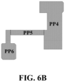
- FIG. 5 F illustrates the structure of first pad in some embodiments according to the present disclosure.
- the first pad in some embodiments includes a first pad part PP 1 , a second pad part PP 2 , and a third pad part PP 3 , the first pad part PP 1 connecting the second pad part PP 2 to the third pad part PP 3 .
- the second pad part PP 2 and the third pad part PP 3 extend from the first pad part PP 1 to a same side (e.g., to the left side).
- An orthographic projection of the first pad part PP 1 on the base substrate at least partially overlaps with an orthographic projection of the respective first reset signal line on the base substrate.
- An orthographic projection of the second pad part PP 2 on the base substrate is at least partially non-overlapping with the orthographic projection of the respective first reset signal line on the base substrate, e.g., the orthographic projection of the second pad part PP 2 on the base substrate is completely non-overlapping with the orthographic projection of the respective first reset signal line on the base substrate.
- An orthographic projection of the third pad part PP 3 on the base substrate is at least partially non-overlapping with the orthographic projection of the respective first reset signal line on the base substrate, e.g., the orthographic projection of the third pad part PP 3 on the base substrate is completely non-overlapping with the orthographic projection of the respective first reset signal line on the base substrate.
- the pixel driving circuits in the (2k-1)-th columns C (2k-1) of the K columns are pixel driving circuits for driving light emission of subpixels of a first color and subpixels of a second color; the pixel driving circuits in the (2k)-th columns C (2k) of the K columns are pixel driving circuits for driving light emission of subpixels of a third color.
- the first color is red
- the second color is blue
- the third color is green.
- the parasitic capacitance at the fourth node N 4 for the pixel driving circuits in the (2k-1)-th columns C (2k-1) of the K columns is greater than the parasitic capacitance at the fourth node N 4 for the pixel driving circuits in the (2k)-th columns C (2k) of the K columns. Accordingly, the higher parasitic capacitance at the fourth node N 4 decreases the light-up speed in the red subpixels and blue subpixels, as compared to the green subpixels.
- the inventors of the present disclosure surprisingly and unexpectedly, discover that the intricate structure of the present array substrate achieves a similar light-up speed in green subpixels, red subpixels, and blue subpixels, obviating the issue of red trailing defects in the related array substrates.
- the second pad PAD 2 is configured to reduce cross-talk between the first node N 1 and an adjacent first pad.
- the second pad PAD 2 is connected to a respective voltage supply line of the plurality of voltage supply lines Vdd in an adjacent pixel driving circuit through a seventh via v 7 extending through the first planarization layer PLN 1 .
- the respective voltage supply line of the plurality of voltage supply lines Vdd is connected to the second capacitor electrode Ce 2 through an eighth via v 8 extending through the inter-layer dielectric layer ILD.
- FIG. 6 A illustrates the structure of a first signal line layer and a second signal line layer in some embodiments according to the present disclosure. As shown in FIG. 6 A and FIG.
- an orthographic projection of the second pad PAD 2 in a respective pixel driving circuit on the base substrate BS covers at least 50% (e.g., at least 55%, at least 60%, at least 65%, at least 70%, at least 75%, at least 80%, at least 85%, at least 90%, at least 95%, at least 99%, or 100%) of an orthographic projection of the node connecting line Cln in the respective pixel driving circuit on the base substrate BS.
- the orthographic projection of the second pad PAD 2 in the respective pixel driving circuit on the base substrate BS at least partially overlaps with an orthographic projection of the active layer ACT 3 of the third transistor T 3 on the base substrate BS.
- the orthographic projection of the second pad PAD 2 in the respective pixel driving circuit on the base substrate BS covers at least 50% (e.g., at least 55%, at least 60%, at least 65%, at least 70%, at least 75%, at least 80%, at least 85%, at least 90%, at least 95%, at least 99%, or 100%) of an orthographic projection of the gate protrusion GP of a respective gate line of the plurality of gate lines GL on the base substrate BS.
- FIG. 6 B illustrates the structure of a second pad in some embodiments according to the present disclosure.
- the second pad in some embodiments includes a fourth pad part PP 4 , a fifth pad part PP 5 , and a sixth pad part PP 6 .
- the fifth pad part PP 5 connects the fourth pad part PP 4 to the sixth pad part PP 6 .
- an orthographic projection of the fourth pad part PP 4 on the base substrate BS at least partially overlaps with the orthographic projection of the node connecting line Cln in the respective pixel driving circuit on the base substrate BS, and at least partially overlaps with the orthographic projection of the gate protrusion GP of the respective gate line of the plurality of gate lines GL on the base substrate BS.
- An orthographic projection of the sixth pad part PP 6 on the base substrate BS at least partially overlaps with an orthographic projection of a respective voltage supply line of the plurality of voltage supply lines Vdd in an adjacent pixel driving circuit on the base substrate BS.
- the fifth pad part PP 5 crosses over a respective data line of the plurality of data lines DL in the adjacent pixel driving circuit.
- the adjacent pixel driving circuit and the respective pixel driving circuit are in a same row along the first direction DR 1 .
- the first pad PAD 1 is connected to a first relay electrode RE 1 in the first signal line layer SL 1 through a ninth via v 9 extending through the first planarization layer PLN 1 , and is connected to a second relay electrode RE 2 in the first signal line layer SL 1 through a tenth via v 10 extending through the first planarization layer PLN 1 .
- the first relay electrode RE 1 is connected to the second electrode D 5 of the fifth transistor T 5 through an eleventh via v 11 extending through the inter-layer dielectric layer ILD, the insulating layer IN, and the gate insulating layer GI.
- the second relay electrode RE 2 is connected to the second electrode D 6 of the sixth transistor T 6 through a twelfth via v 12 extending through the inter-layer dielectric layer ILD, the insulating layer IN, and the gate insulating layer GI.
- the anode connecting pad ACP is connected to the first pad PAD 1 through a thirteenth via v 13 extending through the second planarization layer PLN 2 .
- the anode AD is connected to the anode connecting pad ACP through a fourteenth via v 14 extending through a third planarization layer PLN 3 .
- FIG. 7 is a schematic diagram illustrating a display area and a peripheral area in an array substrate in some embodiments according to the present disclosure.
- the array substrate includes a display area DA and a peripheral area PA.
- the peripheral area PA includes a first sub-area PA 1 on a first side S 1 of the display area DA, a second sub-area PA 2 on a second side S 2 of the display area DA, a third sub-area PA 3 on a third side S 3 of the display area DA, and a fourth sub-area PA 4 on a fourth side S 4 of the display area DA.
- the first side S 1 and the third side S 3 are opposite to each other.
- the second side S 2 and the fourth side S 4 are opposite to each other.
- the first sub-area PA 1 is a sub-area where signal lines of the array substrate are connected to an integrated circuit.
- the term “display area” refers to an area of an array substrate where image is actually displayed.
- the display area may include both a subpixel region and an inter-subpixel region.
- a subpixel region refers to a light emission region of a subpixel, such as a region corresponding to a pixel electrode in a liquid crystal display or a region corresponding to a light emissive layer in an organic light emitting diode display panel.
- An inter-subpixel region refers to a region between adjacent subpixel regions, such as a region corresponding to a black matrix in a liquid crystal display or a region corresponding to a pixel definition layer in an organic light emitting diode display panel.
- the inter-subpixel region is a region between adjacent subpixel regions in a same pixel.
- the inter-subpixel region is a region between two adjacent subpixel regions from two adjacent pixels.
- peripheral area refers to an area of an array substrate in a display panel where various circuits and wires are provided to transmit signals to the display substrate.
- non-transparent or opaque components of the display apparatus e.g., battery, printed circuit board, metal frame
- the peripheral area rather than in the display areas.
- the first sub-area PA 1 includes a side region SR and one or more corner regions (e.g., a first corner region CR 1 and a second corner region CR 2 ).
- the one or more corner regions are respectively at a corner of the display panel.
- the one or more corner regions respectively connect the side region SR to one or more adjacent sub-areas of the peripheral area PA.
- the first corner region CR 1 connects the side region SR to the second sub-area PA 2
- the second corner region CR 2 connects the side region SR to the fourth sub-area PA 4 .
- FIG. 8 is a schematic diagram illustrating a display area and a peripheral area in an array substrate in some embodiments according to the present disclosure.
- the array substrate has an additional display area ADA in addition to the display area DA.
- the additional display area ADA extends away from the display area DA into the side region SR in FIG. 7 , resulting in a reduced side region.
- pixel driving circuits are disposed in the display area DA.
- FIG. 9 illustrates an arrangement of pixel driving circuits and light emitting layers in a region around a border between a display area and an additional display area in some embodiments according to the present disclosure.
- the plurality of anode connecting pads ACP connecting a respective pixel driving circuit PDC and a respective light emitting layer EL extends from the display area DA into the additional display area ADA.
- the additional display area ADA is absent of pixel driving circuits, and includes other components such as power supply lines.
- FIG. 10 illustrates an arrangement of pixel driving circuits and light emitting layers in a region around a border between a display area and an additional display area in some embodiments according to the present disclosure.
- the region may provide space for receiving light emitting layers (denoted as PEL in FIG. 10 ) from previous rows of pixel driving circuit.
- FIG. 11 A illustrates the structure of a respective pixel driving circuit and a respective light emitting element in some embodiments according to the present disclosure.
- FIG. 11 B illustrates the structure of a semiconductor material layer in an array substrate depicted in FIG. 11 A .
- FIG. 11 C illustrates the structure of a first conductive layer in an array substrate depicted in FIG. 11 A .
- FIG. 11 D illustrates the structure of an insulating layer in an array substrate depicted in FIG. 11 A .
- FIG. 11 E illustrates the structure of a second conductive layer in an array substrate depicted in FIG. 11 A .
- FIG. 11 F illustrates the structure of a first signal line layer in an array substrate depicted in FIG. 11 A .
- FIG. 11 B illustrates the structure of a semiconductor material layer in an array substrate depicted in FIG. 11 A .
- FIG. 11 C illustrates the structure of a first conductive layer in an array substrate depicted in FIG. 11 A .
- FIG. 11 D
- FIG. 11 G illustrates the structure of a second signal line layer in an array substrate depicted in FIG. 11 A .
- FIG. 11 H illustrates the structure of a third signal line layer in an array substrate depicted in FIG. 11 A .
- FIG. 11 I illustrates the structure of an anode layer in an array substrate depicted in FIG. 11 A .
- FIG. 11 J illustrates the structure of a pixel definition layer in an array substrate depicted in FIG. 11 A .
- FIG. 11 K illustrates the structure of a light emitting layer in an array substrate depicted in FIG. 11 A .
- FIG. 12 A is a cross-sectional view along a G-G′ line in FIG. 11 A .
- FIG. 12 B is a cross-sectional view along an H-H′ line in FIG. 11 A .
- the array substrate includes a base substrate BS, a semiconductor material layer SML on the base substrate BS, a gate insulating layer GI on a side of the semiconductor material layer SML away from the base substrate BS, a first conductive layer Gate 1 on a side of the gate insulating layer GI away from the semiconductor material layer SML, an insulating layer IN on a side of the first conductive layer away from the gate insulating layer GI, a second conductive layer Gate 2 on a side of the insulating layer IN away from the first conductive layer Gate 1 , an inter-layer dielectric layer ILD on a side of the second conductive layer Gate 2 away from the insulating layer IN, a first signal line layer SLL 1 on a side of the inter-layer dielectric layer ILD away from the second conductive layer Gate 2 , a first planarization layer PLN 1 on a side of the first signal
- the semiconductor material layer SML in some embodiments includes active layers of the transistors, including active layers of the first transistor T 1 , the second transistor T 2 , the third transistor T 3 , the fourth transistor T 4 , the fifth transistor T 5 , the sixth transistor T 6 , and the driving transistor Td.
- Various appropriate semiconductor materials may be used for making the semiconductor material layer SML. Examples of appropriate semiconductor materials for making the semiconductor material layer SML include polycrystalline silicon, amorphous silicon, and metal oxides.
- the first conductive layer Gate 1 in some embodiments includes a plurality of gate lines GL, a plurality of reset control signal lines rst, a plurality of light emitting control signal lines em, and a first capacitor electrode Ce 1 of the storage capacitor Cst.
- Vias extending through an insulating layer IN are depicted in FIG. 11 D .
- the second conductive layer Gate 2 in some embodiments includes an interference preventing block IPB, a second capacitor electrode Ce 2 of the storage capacitor Cst, and a plurality of first reset signal lines Vintr.
- the interference preventing block IPB can effectively reduce crosstalk, particularly vertical crosstalk between the N 1 node and the adjacent data lines.
- the first signal line layer SLL 1 in some embodiments includes a plurality of voltage supply lines Vdd, a node connecting line Cln, a plurality of second reset signal lines Vintc, and a plurality of data lines DL.
- the node connecting line Cln connects the first capacitor electrode Ce 1 and the drain electrode of the third transistor T 3 in a respective pixel driving circuit together.
- the array substrate further includes a first via v 1 in the hole region H and extending through the inter-layer dielectric layer ILD and the insulating layer IN.
- the node connecting line Cln is connected to the first capacitor electrode Ce 1 through the first via v 1 .
- the first capacitor electrode Ce 1 is on a side of the gate insulating layer GI away from the base substrate BS.
- the array substrate further includes a second via v 2 .
- the first via v 1 is in the hole region H and extends through the inter-layer dielectric layer ILD and the insulating layer IN.
- the second via v 2 extends through the inter-layer dielectric layer ILD, the insulating layer IN, and the gate insulating layer GI.
- the node connecting line Cln is connected to the first capacitor electrode Ce 1 through the first via v 1 , and is connected to the semiconductor material layer SML through the second via v 2 .
- the node connecting line Cln is connected to the drain electrode D 3 of third transistor, as depicted in FIG. 12 A .
- the second signal line layer SLL 2 in some embodiments includes a connecting pad CP, through which the N 4 node is electrically connected to an anode of the respective light emitting element.
- the array substrate further includes a third via v 3 extending through the first planarization layer PLN 1 , the inter-layer dielectric layer ILD, the insulating layer IN, and the gate insulating layer GI.
- the connecting pad CP is connected to the N 4 node through the third via v 3 .
- the anode connecting pad layer ACPL in some embodiments includes a plurality of anode connecting pads ACP.
- a respective anode connecting pad of the plurality of anode connecting pads ACP electrically connects the connecting pad CP to an anode of the respective light emitting element.
- the array substrate further includes a fourth via v 4 extending through the second planarization layer PLN 2 .
- a respective anode connecting pad of the plurality of anode connecting pads ACP is connected to the connecting pad CP through the fourth via v 4 .
- Various appropriate conductive materials may be used for making the plurality of anode connecting pads ACP. Examples of appropriate conductive materials for making the plurality of anode connecting pads ACP include conductive metal oxides such as indium tin oxide.
- the anode layer includes a plurality of anodes AD of a plurality of light emitting elements.
- a respective anode of the plurality of anodes AD is connected to a respective connecting line.
- the array substrate further includes a fifth via v 5 extending through the third planarization layer PLN 3 .
- the respective anode is connected to the respective connecting line through the fifth via v 5 .
- the pixel definition layer PDL defines a plurality of subpixel apertures SA.
- the organic layer OL in some embodiments includes a plurality of light emitting layer EML of a plurality of light emitting elements.
- a respective light emitting layer of the plurality of light emitting layer EML is electrically connected to a respective anode of the plurality of anodes AD.
- the plurality of anode connecting pads ACP are in an anode connecting pad layer ACPL; the second planarization layer PLN 2 is on a side of the anode connecting pad layer ACPL closer to a base substrate BS; the third planarization layer PLN 3 is on a side of the anode connecting pad layer ACPL away from the base substrate BS; the anode layer ADL is on a side of the third planarization layer PLN 3 away from the anode connecting pad layer ACPL; and the plurality of pixel driving circuits PDC are on a side of the second planarization layer PLN 2 away from the anode connecting pad layer ACPL.
- FIG. 13 A illustrates the structure of an array substrate in a second region in some embodiments according to the present disclosure.
- FIG. 13 B illustrates the structure of pixel driving circuits in FIG. 13 A .
- FIG. 13 C illustrates the structure of connecting lines in FIG. 13 A .
- FIG. 13 D illustrates the structure of light emitting elements in FIG. 13 A .
- the additional display area ADA multiple light emitting elements of a plurality of light emitting elements LE are present, and transistors and capacitors of the plurality of pixel driving circuits PDC are absent.
- the additional display area ADA at least one row of light emitting elements are present, and transistors and capacitors of the plurality of pixel driving circuits PDC are absent.
- the display area DA multiple rows of light emitting elements and transistors and capacitors of multiple rows of pixel driving circuits are present.
- the plurality of anode connecting pads ACP connect the plurality of pixel driving circuits PDC with a plurality of corresponding light emitting elements, respectively.
- a respective anode connecting pad RACP connects a respective pixel driving circuit RPDC with a respective light emitting element RLE.
- FIG. 14 illustrates the structure of an anode connecting pad layer, an anode layer, and a light emitting layer in some embodiments according to the present disclosure.
- the anode connecting pad layer includes a plurality of anode connecting pads ACP
- the anode layer includes a plurality of anodes AD
- the light emitting layer includes a plurality of light emitting blocks EMB.
- FIG. 14 depicts the layout of a plurality of anode connecting pads ACP, a plurality of anodes AD, and a plurality of light emitting blocks EMB in an additional display area.
- the plurality of subpixels includes a respective first subpixel sp 1 , a respective second subpixel sp 2 , a respective third subpixel sp 3 , and a respective fourth subpixel sp 4 .
- a respective pixel of the array substrate includes the respective first subpixel sp 1 , the respective second subpixel sp 2 , the respective third subpixel sp 3 , and the respective fourth subpixel sp 4 .
- the respective first subpixel sp 1 is a red subpixel
- the respective second subpixel sp 2 is a green subpixel
- the respective third subpixel sp 3 is a blue subpixel
- the respective fourth subpixel sp 4 is a green subpixel.
- an orthographic projection of the plurality of anode connecting pads ACP on a base substrate partially overlaps with an orthographic projection of the respective first subpixel sp 1 on the base substrate, resulting in a first overlapping area; an orthographic projection of the plurality of anode connecting pads ACP on a base substrate partially overlaps with an orthographic projection of the respective second subpixel sp 2 on the base substrate, resulting in a second overlapping area; an orthographic projection of the plurality of anode connecting pads ACP on a base substrate partially overlaps with an orthographic projection of the respective third subpixel sp 3 on the base substrate, resulting in a third overlapping area; or an orthographic projection of the plurality of anode connecting pads ACP on a base substrate partially overlaps with an orthographic projection of the respective fourth subpixel sp 4 on the base substrate, resulting in a fourth overlapping area.
- the first overlapping area is greater than the second overlapping area, e.g., by at least 1%, by at least 2.5%, by at least 5%, by at least 7.5%, by at least 10%, by at least 12.5%, by at least 15%, by at least 17.5%, by at least 20%, by at least 22.5%, by at least 25%, by at least 27.5%, by at least 30%, by at least 32.5%, by at least 35%, by at least 37.5%, or by at least 40%.
- the first overlapping area is greater than the fourth overlapping area, e.g., by at least 1%, by at least 2.5%, by at least 5%, by at least 7.5%, by at least 10%, by at least 12.5%, by at least 15%, by at least 17.5%, by at least 20%, by at least 22.5%, by at least 25%, by at least 27.5%, by at least 30%, by at least 32.5%, by at least 35%, by at least 37.5%, or by at least 40%.
- the third overlapping area is greater than the second overlapping area, e.g., by at least 1%, by at least 2.5%, by at least 5%, by at least 7.5%, by at least 10%, by at least 12.5%, by at least 15%, by at least 17.5%, by at least 20%, by at least 22.5%, by at least 25%, by at least 27.5%, by at least 30%, by at least 32.5%, by at least 35%, by at least 37.5%, or by at least 40%.
- the third overlapping area is greater than the fourth overlapping area, e.g., by at least 1%, by at least 2.5%, by at least 5%, by at least 7.5%, by at least 10%, by at least 12.5%, by at least 15%, by at least 17.5%, by at least 20%, by at least 22.5%, by at least 25%, by at least 27.5%, by at least 30%, by at least 32.5%, by at least 35%, by at least 37.5%, or by at least 40%.
- the respective first subpixel sp 1 is a red subpixel
- the respective second subpixel sp 2 is a green subpixel
- the respective third subpixel sp 3 is a blue subpixel
- the respective fourth subpixel sp 4 is a green subpixel.
- the parasitic capacitance for the pixel driving circuits in the red subpixel and the blue subpixel is greater than the parasitic capacitance for the pixel driving circuits in the green subpixel.
- the higher parasitic capacitance decreases the light-up speed in the red subpixels and blue subpixels, as compared to the green subpixels.
- the inventors of the present disclosure surprisingly and unexpectedly, discover that the intricate structure of the present array substrate achieves a similar light-up speed in green subpixels, red subpixels, and blue subpixels, obviating the issue of red trailing defects in the related array substrates.
- the present invention provides a display apparatus, including the array substrate described herein or fabricated by a method described herein, and one or more integrated circuits connected to the array substrate.
- display apparatuses include, but are not limited to, an electronic paper, a mobile phone, a tablet computer, a television, a monitor, a notebook computer, a digital album, a GPS, etc.
- the display apparatus is an organic light emitting diode display apparatus.
- the display apparatus is a liquid crystal display apparatus.
- the present invention provides a method of fabricating an array substrate.
- the method includes forming K number of columns of first pads.
- a respective first pad is formed to be connected to an anode of a light emitting element, a second electrode of a fifth transistor, and a second electrode of a sixth transistor.
- forming the K number of columns of first pads includes forming a plurality of first-first pads in (2k-1)-th columns of the K columns and a plurality of second-first pads in (2k)-th columns of the K columns.
- a respective first-first pad and a respective second-first pad are formed to have different average line widths.
- the term “the invention”, “the present invention” or the like does not necessarily limit the claim scope to a specific embodiment, and the reference to exemplary embodiments of the invention does not imply a limitation on the invention, and no such limitation is to be inferred.
- the invention is limited only by the spirit and scope of the appended claims. Moreover, these claims may refer to use “first”, “second”, etc. following with noun or element. Such terms should be understood as a nomenclature and should not be construed as giving the limitation on the number of the elements modified by such nomenclature unless specific number has been given. Any advantages and benefits described may not apply to all embodiments of the invention.
Landscapes
- Engineering & Computer Science (AREA)
- Physics & Mathematics (AREA)
- Computer Hardware Design (AREA)
- General Physics & Mathematics (AREA)
- Theoretical Computer Science (AREA)
- Microelectronics & Electronic Packaging (AREA)
- Devices For Indicating Variable Information By Combining Individual Elements (AREA)
- Electroluminescent Light Sources (AREA)
Abstract
Description
Claims (19)
Applications Claiming Priority (1)
| Application Number | Priority Date | Filing Date | Title |
|---|---|---|---|
| PCT/CN2022/123115 WO2024065624A1 (en) | 2022-09-30 | 2022-09-30 | Array substrate and display apparatus |
Publications (2)
| Publication Number | Publication Date |
|---|---|
| US20240363072A1 US20240363072A1 (en) | 2024-10-31 |
| US12190822B2 true US12190822B2 (en) | 2025-01-07 |
Family
ID=90475561
Family Applications (1)
| Application Number | Title | Priority Date | Filing Date |
|---|---|---|---|
| US18/255,100 Active US12190822B2 (en) | 2022-09-30 | 2022-09-30 | Array substrate and display apparatus |
Country Status (4)
| Country | Link |
|---|---|
| US (1) | US12190822B2 (en) |
| EP (1) | EP4458117A4 (en) |
| CN (1) | CN118120352B (en) |
| WO (1) | WO2024065624A1 (en) |
Citations (16)
| Publication number | Priority date | Publication date | Assignee | Title |
|---|---|---|---|---|
| US20060261732A1 (en) | 2005-05-23 | 2006-11-23 | Eastman Kodak Company | Color organic light-emitting diode display with improved lifetime |
| US20120050344A1 (en) * | 2010-08-24 | 2012-03-01 | Samsung Mobile Display Co., Ltd. | Organic Light Emitting Display Having Uniform Brightness |
| CN103915571A (en) | 2014-01-27 | 2014-07-09 | 上海天马有机发光显示技术有限公司 | AMOLED display panel and film manufacturing method and display device |
| CN109065568A (en) | 2018-07-06 | 2018-12-21 | 青岛海信电器股份有限公司 | A kind of WOLED panel and WOLED display device |
| US20200286432A1 (en) * | 2016-08-22 | 2020-09-10 | Ordos Yuansheng Optoelectronics Co., Ltd. | Pixel circuit, display panel, display device and driving method |
| CN112086467A (en) | 2020-09-02 | 2020-12-15 | 武汉华星光电半导体显示技术有限公司 | Display panel |
| CN113658995A (en) | 2021-10-20 | 2021-11-16 | 北京京东方技术开发有限公司 | Display substrate, touch display panel and display device |
| US20220157921A1 (en) | 2020-03-19 | 2022-05-19 | Chengdu Boe Optoelectronics Technology Co., Ltd. | Display substrate and display device |
| WO2022160255A1 (en) | 2021-01-29 | 2022-08-04 | Boe Technology Group Co., Ltd. | Array substrate and display apparatus |
| WO2022165717A1 (en) | 2021-02-04 | 2022-08-11 | 京东方科技集团股份有限公司 | Array substrate and display apparatus |
| US20220320247A1 (en) * | 2020-04-26 | 2022-10-06 | Chengdu Boe Optoelectronics Technology Co., Ltd. | Display substrate and display device |
| US20220359577A1 (en) * | 2021-05-06 | 2022-11-10 | Samsung Display Co Ltd | Light emitting display device |
| US20220376024A1 (en) * | 2020-09-28 | 2022-11-24 | Boe Technology Group Co., Ltd. | Display Substrate and Manufacturing Method Therefor, and Display Apparatus |
| CN115668343A (en) | 2022-08-30 | 2023-01-31 | 京东方科技集团股份有限公司 | Array substrate and display device |
| US20230133179A1 (en) * | 2020-05-06 | 2023-05-04 | Chengdu Boe Optoelectronics Technology Co., Ltd. | Display substrate and drive method thereof, and display device |
| US20230238487A1 (en) * | 2022-01-24 | 2023-07-27 | Samsung Display Co., Ltd. | Display device |
Family Cites Families (7)
| Publication number | Priority date | Publication date | Assignee | Title |
|---|---|---|---|---|
| JP2010164765A (en) * | 2009-01-15 | 2010-07-29 | Toshiba Mobile Display Co Ltd | Liquid crystal display device |
| KR102605283B1 (en) | 2016-06-30 | 2023-11-27 | 삼성디스플레이 주식회사 | Display device |
| KR102638304B1 (en) * | 2016-08-02 | 2024-02-20 | 삼성디스플레이 주식회사 | Display apparatus |
| KR102774342B1 (en) * | 2017-02-07 | 2025-03-05 | 삼성디스플레이 주식회사 | Organic light emitting display device |
| CN107369692B (en) * | 2017-06-09 | 2021-04-30 | 厦门天马微电子有限公司 | Display panel and display device |
| US20200118193A1 (en) * | 2018-10-12 | 2020-04-16 | International Business Machines Corporation | Digital content publisher negotiated transactional advertiser |
| WO2022082333A1 (en) * | 2020-10-19 | 2022-04-28 | Boe Technology Group Co., Ltd. | Array substrate and display apparatus |
-
2022
- 2022-09-30 EP EP22960251.1A patent/EP4458117A4/en active Pending
- 2022-09-30 US US18/255,100 patent/US12190822B2/en active Active
- 2022-09-30 CN CN202280003406.8A patent/CN118120352B/en active Active
- 2022-09-30 WO PCT/CN2022/123115 patent/WO2024065624A1/en not_active Ceased
Patent Citations (18)
| Publication number | Priority date | Publication date | Assignee | Title |
|---|---|---|---|---|
| US20060261732A1 (en) | 2005-05-23 | 2006-11-23 | Eastman Kodak Company | Color organic light-emitting diode display with improved lifetime |
| US20120050344A1 (en) * | 2010-08-24 | 2012-03-01 | Samsung Mobile Display Co., Ltd. | Organic Light Emitting Display Having Uniform Brightness |
| CN103915571A (en) | 2014-01-27 | 2014-07-09 | 上海天马有机发光显示技术有限公司 | AMOLED display panel and film manufacturing method and display device |
| US20150214505A1 (en) | 2014-01-27 | 2015-07-30 | Shanghai Tianma AM-OLED Co., Ltd. | Amoled display panel, method of fabricating film layer and display apparatus |
| US20200286432A1 (en) * | 2016-08-22 | 2020-09-10 | Ordos Yuansheng Optoelectronics Co., Ltd. | Pixel circuit, display panel, display device and driving method |
| CN109065568A (en) | 2018-07-06 | 2018-12-21 | 青岛海信电器股份有限公司 | A kind of WOLED panel and WOLED display device |
| US20220157921A1 (en) | 2020-03-19 | 2022-05-19 | Chengdu Boe Optoelectronics Technology Co., Ltd. | Display substrate and display device |
| US20220320247A1 (en) * | 2020-04-26 | 2022-10-06 | Chengdu Boe Optoelectronics Technology Co., Ltd. | Display substrate and display device |
| US20230133179A1 (en) * | 2020-05-06 | 2023-05-04 | Chengdu Boe Optoelectronics Technology Co., Ltd. | Display substrate and drive method thereof, and display device |
| CN112086467A (en) | 2020-09-02 | 2020-12-15 | 武汉华星光电半导体显示技术有限公司 | Display panel |
| US20220376024A1 (en) * | 2020-09-28 | 2022-11-24 | Boe Technology Group Co., Ltd. | Display Substrate and Manufacturing Method Therefor, and Display Apparatus |
| WO2022160255A1 (en) | 2021-01-29 | 2022-08-04 | Boe Technology Group Co., Ltd. | Array substrate and display apparatus |
| WO2022165717A1 (en) | 2021-02-04 | 2022-08-11 | 京东方科技集团股份有限公司 | Array substrate and display apparatus |
| US20230180550A1 (en) | 2021-02-04 | 2023-06-08 | Boe Technology Group Co., Ltd. | Array substrate and display device |
| US20220359577A1 (en) * | 2021-05-06 | 2022-11-10 | Samsung Display Co Ltd | Light emitting display device |
| CN113658995A (en) | 2021-10-20 | 2021-11-16 | 北京京东方技术开发有限公司 | Display substrate, touch display panel and display device |
| US20230238487A1 (en) * | 2022-01-24 | 2023-07-27 | Samsung Display Co., Ltd. | Display device |
| CN115668343A (en) | 2022-08-30 | 2023-01-31 | 京东方科技集团股份有限公司 | Array substrate and display device |
Non-Patent Citations (1)
| Title |
|---|
| International Search Report & Written Opinion mailed May 17, 2023, regarding PCT/CN2022/123115. |
Also Published As
| Publication number | Publication date |
|---|---|
| US20240363072A1 (en) | 2024-10-31 |
| CN118120352A (en) | 2024-05-31 |
| EP4458117A1 (en) | 2024-11-06 |
| WO2024065624A1 (en) | 2024-04-04 |
| CN118120352B (en) | 2025-09-26 |
| EP4458117A4 (en) | 2025-03-19 |
Similar Documents
| Publication | Publication Date | Title |
|---|---|---|
| US12190803B2 (en) | Array substrate and display apparatus | |
| US12284890B2 (en) | Display panel | |
| US20240365593A1 (en) | Array substrate and display apparatus | |
| US20250169310A1 (en) | Array substrate and display apparatus | |
| US12048216B2 (en) | Array substrate and display apparatus | |
| US20230138949A1 (en) | Array substrate and display apparatus | |
| US20230165059A1 (en) | Display panel | |
| US20250363950A1 (en) | Array substrate and display apparatus | |
| US12518694B2 (en) | Array substrate and display apparatus | |
| US12190822B2 (en) | Array substrate and display apparatus | |
| US20240215348A1 (en) | Array substrate and display apparatus | |
| US20250089494A1 (en) | Array substrate and display apparatus | |
| US12433021B2 (en) | Array substrate and display apparatus | |
| US12536958B2 (en) | Array substrate and display apparatus | |
| US20250089490A1 (en) | Array substrate and display apparatus | |
| US20260051288A1 (en) | Array substrate and display apparatus | |
| US20250228085A1 (en) | Array substrate and display apparatus |
Legal Events
| Date | Code | Title | Description |
|---|---|---|---|
| FEPP | Fee payment procedure |
Free format text: ENTITY STATUS SET TO UNDISCOUNTED (ORIGINAL EVENT CODE: BIG.); ENTITY STATUS OF PATENT OWNER: LARGE ENTITY |
|
| AS | Assignment |
Owner name: BOE TECHNOLOGY GROUP CO., LTD., CHINA Free format text: ASSIGNMENT OF ASSIGNORS INTEREST;ASSIGNORS:WANG, MENGQI;ZHANG, TIAOMEI;LI, ZHENGKUN;AND OTHERS;REEL/FRAME:063852/0078 Effective date: 20230523 Owner name: CHENGDU BOE OPTOELECTRONICS TECHNOLOGY CO., LTD., CHINA Free format text: ASSIGNMENT OF ASSIGNORS INTEREST;ASSIGNORS:WANG, MENGQI;ZHANG, TIAOMEI;LI, ZHENGKUN;AND OTHERS;REEL/FRAME:063852/0078 Effective date: 20230523 |
|
| STPP | Information on status: patent application and granting procedure in general |
Free format text: NOTICE OF ALLOWANCE MAILED -- APPLICATION RECEIVED IN OFFICE OF PUBLICATIONS |
|
| STPP | Information on status: patent application and granting procedure in general |
Free format text: PUBLICATIONS -- ISSUE FEE PAYMENT RECEIVED |
|
| STPP | Information on status: patent application and granting procedure in general |
Free format text: PUBLICATIONS -- ISSUE FEE PAYMENT VERIFIED |
|
| STCF | Information on status: patent grant |
Free format text: PATENTED CASE |