US12190811B2 - Display substrate and display apparatus - Google Patents
Display substrate and display apparatus Download PDFInfo
- Publication number
- US12190811B2 US12190811B2 US18/268,361 US202118268361A US12190811B2 US 12190811 B2 US12190811 B2 US 12190811B2 US 202118268361 A US202118268361 A US 202118268361A US 12190811 B2 US12190811 B2 US 12190811B2
- Authority
- US
- United States
- Prior art keywords
- transistor
- electrode
- signal line
- clock signal
- gate
- Prior art date
- Legal status (The legal status is an assumption and is not a legal conclusion. Google has not performed a legal analysis and makes no representation as to the accuracy of the status listed.)
- Active
Links
Images


Classifications
-
- G—PHYSICS
- G09—EDUCATION; CRYPTOGRAPHY; DISPLAY; ADVERTISING; SEALS
- G09G—ARRANGEMENTS OR CIRCUITS FOR CONTROL OF INDICATING DEVICES USING STATIC MEANS TO PRESENT VARIABLE INFORMATION
- G09G3/00—Control arrangements or circuits, of interest only in connection with visual indicators other than cathode-ray tubes
- G09G3/20—Control arrangements or circuits, of interest only in connection with visual indicators other than cathode-ray tubes for presentation of an assembly of a number of characters, e.g. a page, by composing the assembly by combination of individual elements arranged in a matrix no fixed position being assigned to or needed to be assigned to the individual characters or partial characters
- G09G3/22—Control arrangements or circuits, of interest only in connection with visual indicators other than cathode-ray tubes for presentation of an assembly of a number of characters, e.g. a page, by composing the assembly by combination of individual elements arranged in a matrix no fixed position being assigned to or needed to be assigned to the individual characters or partial characters using controlled light sources
- G09G3/30—Control arrangements or circuits, of interest only in connection with visual indicators other than cathode-ray tubes for presentation of an assembly of a number of characters, e.g. a page, by composing the assembly by combination of individual elements arranged in a matrix no fixed position being assigned to or needed to be assigned to the individual characters or partial characters using controlled light sources using electroluminescent panels
- G09G3/32—Control arrangements or circuits, of interest only in connection with visual indicators other than cathode-ray tubes for presentation of an assembly of a number of characters, e.g. a page, by composing the assembly by combination of individual elements arranged in a matrix no fixed position being assigned to or needed to be assigned to the individual characters or partial characters using controlled light sources using electroluminescent panels semiconductive, e.g. using light-emitting diodes [LED]
- G09G3/3208—Control arrangements or circuits, of interest only in connection with visual indicators other than cathode-ray tubes for presentation of an assembly of a number of characters, e.g. a page, by composing the assembly by combination of individual elements arranged in a matrix no fixed position being assigned to or needed to be assigned to the individual characters or partial characters using controlled light sources using electroluminescent panels semiconductive, e.g. using light-emitting diodes [LED] organic, e.g. using organic light-emitting diodes [OLED]
- G09G3/3225—Control arrangements or circuits, of interest only in connection with visual indicators other than cathode-ray tubes for presentation of an assembly of a number of characters, e.g. a page, by composing the assembly by combination of individual elements arranged in a matrix no fixed position being assigned to or needed to be assigned to the individual characters or partial characters using controlled light sources using electroluminescent panels semiconductive, e.g. using light-emitting diodes [LED] organic, e.g. using organic light-emitting diodes [OLED] using an active matrix
- G09G3/3233—Control arrangements or circuits, of interest only in connection with visual indicators other than cathode-ray tubes for presentation of an assembly of a number of characters, e.g. a page, by composing the assembly by combination of individual elements arranged in a matrix no fixed position being assigned to or needed to be assigned to the individual characters or partial characters using controlled light sources using electroluminescent panels semiconductive, e.g. using light-emitting diodes [LED] organic, e.g. using organic light-emitting diodes [OLED] using an active matrix with pixel circuitry controlling the current through the light-emitting element
-
- G—PHYSICS
- G09—EDUCATION; CRYPTOGRAPHY; DISPLAY; ADVERTISING; SEALS
- G09G—ARRANGEMENTS OR CIRCUITS FOR CONTROL OF INDICATING DEVICES USING STATIC MEANS TO PRESENT VARIABLE INFORMATION
- G09G3/00—Control arrangements or circuits, of interest only in connection with visual indicators other than cathode-ray tubes
- G09G3/20—Control arrangements or circuits, of interest only in connection with visual indicators other than cathode-ray tubes for presentation of an assembly of a number of characters, e.g. a page, by composing the assembly by combination of individual elements arranged in a matrix no fixed position being assigned to or needed to be assigned to the individual characters or partial characters
- G09G3/22—Control arrangements or circuits, of interest only in connection with visual indicators other than cathode-ray tubes for presentation of an assembly of a number of characters, e.g. a page, by composing the assembly by combination of individual elements arranged in a matrix no fixed position being assigned to or needed to be assigned to the individual characters or partial characters using controlled light sources
- G09G3/30—Control arrangements or circuits, of interest only in connection with visual indicators other than cathode-ray tubes for presentation of an assembly of a number of characters, e.g. a page, by composing the assembly by combination of individual elements arranged in a matrix no fixed position being assigned to or needed to be assigned to the individual characters or partial characters using controlled light sources using electroluminescent panels
- G09G3/32—Control arrangements or circuits, of interest only in connection with visual indicators other than cathode-ray tubes for presentation of an assembly of a number of characters, e.g. a page, by composing the assembly by combination of individual elements arranged in a matrix no fixed position being assigned to or needed to be assigned to the individual characters or partial characters using controlled light sources using electroluminescent panels semiconductive, e.g. using light-emitting diodes [LED]
- G09G3/3208—Control arrangements or circuits, of interest only in connection with visual indicators other than cathode-ray tubes for presentation of an assembly of a number of characters, e.g. a page, by composing the assembly by combination of individual elements arranged in a matrix no fixed position being assigned to or needed to be assigned to the individual characters or partial characters using controlled light sources using electroluminescent panels semiconductive, e.g. using light-emitting diodes [LED] organic, e.g. using organic light-emitting diodes [OLED]
- G09G3/3266—Details of drivers for scan electrodes
-
- G—PHYSICS
- G11—INFORMATION STORAGE
- G11C—STATIC STORES
- G11C19/00—Digital stores in which the information is moved stepwise, e.g. shift registers
- G11C19/28—Digital stores in which the information is moved stepwise, e.g. shift registers using semiconductor elements
-
- G—PHYSICS
- G09—EDUCATION; CRYPTOGRAPHY; DISPLAY; ADVERTISING; SEALS
- G09G—ARRANGEMENTS OR CIRCUITS FOR CONTROL OF INDICATING DEVICES USING STATIC MEANS TO PRESENT VARIABLE INFORMATION
- G09G2300/00—Aspects of the constitution of display devices
- G09G2300/04—Structural and physical details of display devices
- G09G2300/0404—Matrix technologies
- G09G2300/0408—Integration of the drivers onto the display substrate
-
- G—PHYSICS
- G09—EDUCATION; CRYPTOGRAPHY; DISPLAY; ADVERTISING; SEALS
- G09G—ARRANGEMENTS OR CIRCUITS FOR CONTROL OF INDICATING DEVICES USING STATIC MEANS TO PRESENT VARIABLE INFORMATION
- G09G2300/00—Aspects of the constitution of display devices
- G09G2300/04—Structural and physical details of display devices
- G09G2300/0421—Structural details of the set of electrodes
- G09G2300/0426—Layout of electrodes and connections
-
- G—PHYSICS
- G09—EDUCATION; CRYPTOGRAPHY; DISPLAY; ADVERTISING; SEALS
- G09G—ARRANGEMENTS OR CIRCUITS FOR CONTROL OF INDICATING DEVICES USING STATIC MEANS TO PRESENT VARIABLE INFORMATION
- G09G2300/00—Aspects of the constitution of display devices
- G09G2300/08—Active matrix structure, i.e. with use of active elements, inclusive of non-linear two terminal elements, in the pixels together with light emitting or modulating elements
- G09G2300/0809—Several active elements per pixel in active matrix panels
- G09G2300/0819—Several active elements per pixel in active matrix panels used for counteracting undesired variations, e.g. feedback or autozeroing
-
- G—PHYSICS
- G09—EDUCATION; CRYPTOGRAPHY; DISPLAY; ADVERTISING; SEALS
- G09G—ARRANGEMENTS OR CIRCUITS FOR CONTROL OF INDICATING DEVICES USING STATIC MEANS TO PRESENT VARIABLE INFORMATION
- G09G2300/00—Aspects of the constitution of display devices
- G09G2300/08—Active matrix structure, i.e. with use of active elements, inclusive of non-linear two terminal elements, in the pixels together with light emitting or modulating elements
- G09G2300/0809—Several active elements per pixel in active matrix panels
- G09G2300/0842—Several active elements per pixel in active matrix panels forming a memory circuit, e.g. a dynamic memory with one capacitor
- G09G2300/0861—Several active elements per pixel in active matrix panels forming a memory circuit, e.g. a dynamic memory with one capacitor with additional control of the display period without amending the charge stored in a pixel memory, e.g. by means of additional select electrodes
-
- G—PHYSICS
- G09—EDUCATION; CRYPTOGRAPHY; DISPLAY; ADVERTISING; SEALS
- G09G—ARRANGEMENTS OR CIRCUITS FOR CONTROL OF INDICATING DEVICES USING STATIC MEANS TO PRESENT VARIABLE INFORMATION
- G09G2310/00—Command of the display device
- G09G2310/02—Addressing, scanning or driving the display screen or processing steps related thereto
- G09G2310/0262—The addressing of the pixel, in a display other than an active matrix LCD, involving the control of two or more scan electrodes or two or more data electrodes, e.g. pixel voltage dependent on signals of two data electrodes
-
- G—PHYSICS
- G09—EDUCATION; CRYPTOGRAPHY; DISPLAY; ADVERTISING; SEALS
- G09G—ARRANGEMENTS OR CIRCUITS FOR CONTROL OF INDICATING DEVICES USING STATIC MEANS TO PRESENT VARIABLE INFORMATION
- G09G2310/00—Command of the display device
- G09G2310/02—Addressing, scanning or driving the display screen or processing steps related thereto
- G09G2310/0264—Details of driving circuits
- G09G2310/0281—Arrangement of scan or data electrode driver circuits at the periphery of a panel not inherent to a split matrix structure
-
- G—PHYSICS
- G09—EDUCATION; CRYPTOGRAPHY; DISPLAY; ADVERTISING; SEALS
- G09G—ARRANGEMENTS OR CIRCUITS FOR CONTROL OF INDICATING DEVICES USING STATIC MEANS TO PRESENT VARIABLE INFORMATION
- G09G2310/00—Command of the display device
- G09G2310/02—Addressing, scanning or driving the display screen or processing steps related thereto
- G09G2310/0264—Details of driving circuits
- G09G2310/0286—Details of a shift registers arranged for use in a driving circuit
-
- G—PHYSICS
- G09—EDUCATION; CRYPTOGRAPHY; DISPLAY; ADVERTISING; SEALS
- G09G—ARRANGEMENTS OR CIRCUITS FOR CONTROL OF INDICATING DEVICES USING STATIC MEANS TO PRESENT VARIABLE INFORMATION
- G09G2310/00—Command of the display device
- G09G2310/06—Details of flat display driving waveforms
- G09G2310/061—Details of flat display driving waveforms for resetting or blanking
-
- G—PHYSICS
- G09—EDUCATION; CRYPTOGRAPHY; DISPLAY; ADVERTISING; SEALS
- G09G—ARRANGEMENTS OR CIRCUITS FOR CONTROL OF INDICATING DEVICES USING STATIC MEANS TO PRESENT VARIABLE INFORMATION
- G09G2310/00—Command of the display device
- G09G2310/08—Details of timing specific for flat panels, other than clock recovery
-
- G—PHYSICS
- G09—EDUCATION; CRYPTOGRAPHY; DISPLAY; ADVERTISING; SEALS
- G09G—ARRANGEMENTS OR CIRCUITS FOR CONTROL OF INDICATING DEVICES USING STATIC MEANS TO PRESENT VARIABLE INFORMATION
- G09G2320/00—Control of display operating conditions
- G09G2320/04—Maintaining the quality of display appearance
- G09G2320/043—Preventing or counteracting the effects of ageing
- G09G2320/045—Compensation of drifts in the characteristics of light emitting or modulating elements
Definitions
- the present disclosure relates to the field of display technology, and in particular to a display substrate and a display apparatus.
- a display substrate includes a display area and a peripheral area surrounding the display area; a plurality of pixel units arranged in an array are disposed in the display area; a driving module for driving the pixel units is disposed in the peripheral area and includes a plurality of driving circuits; each driving circuit is configured with an independent operating signal line group, and an operating signal line in each operating signal line group is used for providing an electrical signal to a corresponding driving circuit to control the corresponding driving circuit to output.
- the driving module includes Q driving circuits, it is necessary to provide Q operating signal line groups in a one-to-one correspondence with the driving circuits.
- Each driving circuit needs to be operated under the control of at least two different clock signals, so each operating signal line group includes at least two different clock signal lines (a first clock signal line and a second clock signal line).
- at least 2Q clock signal lines need to be arranged in the peripheral area.
- the number of the clock signal lines arranged in the peripheral area is relatively large, so the peripheral area needs to be set to be wider, which is not favorable for realizing a narrow frame.
- the present disclosure provides a display substrate, including: a base substrate, wherein the base substrate includes a display area and a peripheral area surrounding the display area; a plurality of pixel units are in the display area and in an array; a driving module is in the peripheral area; and the driving module is configured to provide electrical signals for the plurality of pixel units, to control the plurality of pixel units to operate; the driving module includes a plurality of driving circuits; each driving circuit is provided with a corresponding operating signal line group in the peripheral area; the operating signal line group includes at least two operating signal lines, which are connected to the corresponding driving circuit, to provide electrical signals to the corresponding driving circuit; the at least two operating signal lines include a first clock signal line and a second clock signal line; the first clock signal lines for at least two of the plurality of driving circuits are a same first clock signal line; and/or the second clock signal lines provided for the at least two of the plurality of driving circuits are a same second clock signal line.
- all the pixel units are divided into a plurality of pixel unit groups, each of which is provided with a first gate line, a second gate line, and a light emitting control signal line corresponding to the pixel unit group; and pixel units in each pixel unit group are connected to the first gate line, the second gate line, and the light emitting control signal line corresponding to the pixel units;
- the plurality of driving circuits include: a first gate driving circuit connected to the first gate line to provide a first gate driving signal to the pixel units corresponding to the first gate line through the first gate line, a second gate driving circuit connected to the second gate line to provide a second gate driving signal to the pixel units corresponding to the second gate line through the second gate line, and a light emitting control driving circuit connected to the light emitting control signal line to provide a light emitting control signal to the pixel units corresponding to the light emitting control signal line through the light emitting control signal line; and first clock signal lines for at least two of the first gate driving circuit, the second gate driving circuit
- the first gate driving circuit, the second gate driving circuit, and the light emitting control driving circuit are sequentially arranged in a first direction and in a direction away from the display area.
- the first clock signal lines for the second gate driving circuit and the light emitting control driving circuit are a same first clock signal line, and the second clock signal lines for the second gate driving circuit and the light emitting control driving circuit are a same second clock signal line; and the first clock signal line for the first gate driving circuit and the first clock signal line for the second gate driving circuit are two different first clock signal lines, and the second clock signal line for the first gate driving circuit and the second clock signal line for the second gate driving circuit are two different second clock signal lines.
- the first clock signal line shared by the second gate driving circuit and the light emitting control driving circuit is between the second gate driving circuit and the light emitting control driving circuit; and the second clock signal line shared by the second gate driving circuit and the light emitting control driving circuit is between the second gate driving circuit and the light emitting control driving circuit.
- the first clock signal line and the second clock signal line for the first gate driving circuit are both between the first gate driving circuit and the second gate driving circuit.
- the first clock signal line for the first gate driving circuit, the second gate driving circuit, and the light emitting control driving circuit is a same first clock signal line
- the second clock signal line for the first gate driving circuit, the second gate driving circuit, and the light emitting control driving circuit is a same second clock signal line
- the first clock signal line shared by the first gate driving circuit, the second gate driving circuit, and the light emitting control driving circuit is in an area where the second gate driving circuit is located; and the second clock signal line shared by the first gate driving circuit, the second gate driving circuit and the light emitting control driving circuit is in the area where the second gate driving circuit is located.
- each pixel unit is provided with a corresponding data line, and the first clock signal line and the second clock signal line are in a same layer as the data line; the first clock signal line and the second clock signal line are connected to the corresponding driving circuit through corresponding connecting traces; and the first clock signal line and the second clock signal line extend along a first direction, the connection traces extend along a second direction, and the first direction intersects with the second direction.
- each pixel unit includes: a light emitting device on a side of a layer where the data line is located away from the base substrate; and the light emitting device includes a first electrode, a light emitting layer and a second electrode sequentially arranged along a direction away from the base substrate, and the connecting traces and the first electrode are in a same layer.
- each pixel unit group is further provided with a corresponding first reset signal line; each pixel unit includes: a pixel circuit and a light emitting device, the pixel circuit includes: a first reset circuit, a writing and compensating circuit and a driving transistor; the first reset circuit is connected to a first reset power supply terminal, a control electrode of the driving transistor and the corresponding first reset signal line, and is configured to write a first reset voltage provided by the first reset power supply terminal into the control electrode of the driving transistor in response to control of the first reset signal line; the writing and compensating circuit is connected to a second operating voltage terminal, the control electrode of the driving transistor, a first electrode of the driving transistor, the corresponding data line, the corresponding first gate line, the corresponding second gate line, and the corresponding light emitting control signal line, and is configured to write a data compensation voltage to the control electrode of the driving transistor in response to control of the first gate line and the second gate line, wherein the data compensation voltage is equal to a sum of a data voltage provided by the data line
- the first reset circuit includes a first transistor
- the writing and compensating circuit includes a third transistor, a fourth transistor, and a fifth transistor
- a control electrode of the first transistor is connected to the first reset signal line, a first electrode of the first transistor is connected to the first reset power supply terminal, and a second electrode of the first transistor is connected to the control electrode of the driving transistor
- a control electrode of the third transistor is connected to the first gate line, a first electrode of the third transistor is connected to the data line, and a second electrode of the third transistor is connected to the first electrode of the driving transistor
- a control electrode of the fourth transistor is connected to the light emitting control signal line, a first electrode of the fourth transistor is connected to the second operating voltage terminal, and a second electrode of the fourth transistor is connected to the first electrode of the driving transistor
- a control electrode of the fifth transistor is connected to the second gate line, a first electrode of the fifth transistor is connected to the control electrode of the driving transistor, and a second electrode of the fifth transistor is connected to the second electrode of the driving transistor
- the first transistor is an N-type transistor
- the first reset signal line for the pixel unit group is the second gate line for m pixel unit groups before the pixel unit group
- m is a positive integer
- the first reset circuit includes a first transistor
- the writing and compensating circuit includes a third transistor, a fourth transistor, a fifth transistor, and a seventh transistor; a control electrode of the first transistor is connected to the first reset signal line, a first electrode of the first transistor is connected to the first reset power supply terminal, and a second electrode of the first transistor is connected to a first electrode of the fifth transistor and a second electrode of the seventh transistor; a control electrode of the third transistor is connected to the first gate line, a first electrode of the third transistor is connected to the data line, and a second electrode of the third transistor is connected to the first electrode of the driving transistor; a control electrode of the fourth transistor is connected to the light emitting control signal line, a first electrode of the fourth transistor is connected to the second operating voltage terminal, and a second electrode of the fourth transistor is connected to the first electrode of the driving transistor; a control electrode of the fifth transistor is connected to the first gate line, and a second electrode of the fifth transistor is connected to the second electrode of the driving transistor; a control electrode of the fifth
- the first transistor is a P-type transistor
- the first reset signal line for the pixel unit group is the first gate line for n pixel unit groups before the pixel unit group
- n is a positive integer
- the at least two operating signal lines further include a frame starting signal line; and frame starting signal lines for the second gate driving circuit and the light emitting control driving circuit are a same frame starting signal line.
- the frame starting signal line shared by the second gate driving circuit and the light emitting control driving circuit is between the second gate driving circuit and the light emitting control driving circuit.
- each pixel unit group is further provided with a corresponding second reset signal line; and the pixel circuit further includes: a second transistor; a control electrode of the second transistor is connected to the corresponding second reset signal line, a first electrode of the second transistor is connected to a second reset power supply terminal, and a second electrode of the second transistor is connected to the first terminal of the light emitting device.
- the second transistor is a P-type transistor
- the second reset signal line for the pixel unit group is the first gate line for n pixel unit groups before the pixel unit group
- n is a positive integer
- the pixel circuit further includes: a sixth transistor between the second electrode of the driving transistor and the first terminal of the light emitting device; a control electrode of the sixth transistor is connected to the corresponding light emitting control signal line, a first electrode of the sixth transistor is connected to the second electrode of the driving transistor, and a second electrode of the sixth transistor is connected to the first terminal of the light emitting device; and the sixth transistor is a P-type transistor.
- an embodiment of the present disclosure further provides a display apparatus, including: the display substrate as provided in the first aspect above.
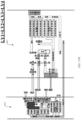
- FIG. 1 is a schematic diagram of a structure of a display substrate according to the present disclosure
- FIG. 2 is a schematic diagram of a structure of a driving module shown in FIG. 1 ;
- FIG. 3 is a schematic diagram of a structure of a display substrate according to an embodiment of the present disclosure.
- FIG. 4 is a schematic diagram of a structure of a driving module shown in FIG. 3 ;
- FIG. 5 is a schematic diagram of another structure of a driving module shown in FIG. 3 ;
- FIG. 6 is a schematic diagram of yet another structure of a driving module shown in FIG. 3 ;
- FIG. 7 is a schematic diagram of a circuit structure of a pixel unit according to an embodiment of the present disclosure.
- FIG. 8 is a schematic diagram of another circuit structure of a pixel unit according to an embodiment of the present disclosure.
- FIG. 9 is a timing diagram illustrating an operation procedure of a pixel unit shown in FIG. 8 ;
- FIG. 10 is a schematic diagram of another circuit structure of a pixel unit according to an embodiment of the present disclosure.
- FIG. 11 is a timing diagram illustrating an operation procedure of a pixel unit shown in FIG. 10 ;
- FIG. 12 is a schematic diagram of a circuit structure of a first shift register according to an embodiment of the present disclosure.
- FIG. 13 is a timing diagram illustrating an operation procedure of a shift register shown in FIG. 12 ;
- FIG. 14 is a schematic diagram of a circuit structure of a second shift register and a third shift register according to an embodiment of the present disclosure
- FIG. 15 is a timing diagram illustrating an operation procedure of a shift register shown in FIG. 14 ;
- FIGS. 16 A to 16 C are schematic diagrams of three different structures for a driving module in FIG. 3 ;
- FIGS. 17 A to 17 O are layouts of partial areas and layouts of respective film layers of a second gate driving circuit and a light emitting control driving circuit when a driving module is shown as in FIG. 16 C ;
- FIG. 18 is a schematic diagram of still another structure of a driving module in FIG. 3 .
- a transistor used may be a thin film transistor or a field effect transistor or any other device with the same and similar characteristics.
- a source electrode and a drain electrode of the transistor used are symmetric to each other, so there is no distinction between the source electrode and the drain electrode.
- one electrode is referred to as a first electrode
- the other electrode is referred to as a second electrode
- a gate electrode is referred to as a control electrode.
- the transistor may be an N-type transistor or a P-type transistor according to the characteristics of the transistor. When the P-type transistor is adopted, the first electrode is a drain electrode of the P-type transistor, the second electrode is a source electrode of the P-type transistor, and the opposite is for the N-type transistor.
- An “active level” in the present disclosure refers to a level at which a corresponding transistor may be controlled to be turned on; specifically, for the P-type transistor, the corresponding active level is low; for the N-type transistor, the corresponding active level is high.
- FIG. 1 is a schematic diagram of a structure of a display substrate according to the present disclosure
- FIG. 2 is a schematic diagram of a structure of a driving module shown in FIG. 1
- the display substrate includes a base substrate including: a display area A (Active area, which may also be referred to as a display effective area or AA area) and a peripheral area B surrounding the display area A, wherein a plurality of pixel units PIX arranged in an array are disposed in the display area A; and a driving module (or driver block) is disposed in the peripheral area B and is configured to provide electrical signals to the pixel units PIX to control the pixel units PIX to operate, and the driving module includes a plurality of driving circuits DC and DC′ to provide a plurality of different electrical signals to the pixel units PIX.
- a display area A Active area, which may also be referred to as a display effective area or AA area
- a driving module or driver block
- the driving module includes a plurality of driving
- Each pixel unit PIX includes a pixel circuit and a light emitting device.
- the pixel circuit includes a transistor and a capacitor, generates an electrical signal (i.e., a driving current) by the transistor and the capacitor, and outputs the electrical signal to the light emitting device to drive the light emitting device to emit light.
- the types and the number of the driving circuits in the driving module are accordingly changed according to different circuit structures of the pixel circuits; the technical solution of the present disclosure does not limit the specific circuit structure of the pixel circuit, and the types and the number of the driving circuits in the driving module.
- each driving circuit DC, DC′ is provided with a corresponding operating signal line group in the peripheral area B.
- the operating signal line group includes at least two operating signal lines, which are connected to the corresponding driving circuit DC, DC′ to provide electrical signals to the corresponding driving circuit DC, DC′.
- the at least two operating signal lines included in the operating signal line group are respectively a first clock signal line and a second clock signal line, which respectively provide a first clock signal and a second clock signal, a duration of the first clock signal in an effective level state is staggered with that of the second clock signal in an effective level state, and the corresponding driving circuit may be controlled to operate based on the first clock signal and the second clock signal.
- the first clock signal lines provided for the at least two driving circuits are a same first clock signal line CK 1 ; and/or the second clock signal lines provided for the at least two driving circuits are a same second clock signal line CK 2 . That is, different driving circuits share a same first clock signal line CK 1 and/or a same second clock signal line CK 2 in the embodiments of the present disclosure.
- Each driving circuit DC, DC′ includes a plurality of cascaded shift registers SR, the first clock signal line CK 1 and the second clock signal line CK 2 provided for the driving circuit DC, DC′ are connected to the shift registers SR within the driving circuit DC, DC′.
- FIG. 1 and FIG. 2 only exemplarily show two driving circuits DC and DC′, and FIG. 2 only exemplarily shows that the two driving circuits share the same first clock signal line CK 1 and the same second clock signal line CK 2 , which is only for illustrative purposes, and does not limit the technical solution of the present disclosure.
- each driving circuit is independently provided with one first clock signal line and one same second clock signal line
- the different driving circuits share the same first clock signal line and/or the same second clock signal line, so that the total number of clock signal lines required to be provided for the entire driving module can be reduced, that is, the total number of operating signal lines can be reduced; at this time, the width of the peripheral area can be reduced correspondingly, which is beneficial to realizing a narrow frame.
- FIG. 3 is a schematic diagram of a structure of a display substrate according to an embodiment of the present disclosure
- FIG. 4 is a schematic diagram of a structure of a driving module shown in FIG. 3
- FIG. 5 is a schematic diagram of another structure of a driving module shown in FIG. 3
- FIG. 6 is a schematic diagram of yet another structure of a driving module shown in FIG. 3 . As shown in FIG. 3 to FIG.
- all pixel units are divided into a plurality of pixel unit groups, each of which is provided with a corresponding first gate line GATE, a corresponding second gate line GATE′ and a corresponding light emitting control signal line EM, and the pixel units are connected to the corresponding first gate line GATE, the corresponding second gate line GATE′ and the corresponding light emitting control signal line EM.
- the plurality of driving circuits includes: a first gate driving circuit DC 1 , a second gate driving circuit DC 2 , and a light emitting control driving circuit DC 3 , the first gate driving circuit DC 1 is connected to the first gate line GATE to provide a first gate driving signal to the pixel unit through the first gate line GATE, the second gate driving circuit DC 2 is connected to the second gate line GATE′ to provide a second gate driving signal to the pixel unit through the second gate line GATE′, the light emitting control driving circuit DC 3 is connected to the light emitting control signal line EM to provide a light emitting control signal to the pixel unit through the light emitting control signal line EM; at least two of the first gate driving circuit DC 1 , the second gate driving circuit DC 2 , and the light emitting control driving circuit DC 3 are provided with the same first clock signal line, and/or with the same second clock signal line.
- FIG. 4 exemplarily shows that the first gate driving circuit DC 1 and the second gate driving circuit DC 2 share a first clock signal line CK 1 , the second gate driving circuit DC 2 and the light emitting control driving circuit DC 3 share a second clock signal line CK 2 ′, the first gate driving circuit DC 1 is provided with an independent second clock signal line CK 2 , and the light emitting control driving circuit DC 3 is provided with an independent first clock signal line CK 1 ′;
- FIG. 4 exemplarily shows that the first gate driving circuit DC 1 and the second gate driving circuit DC 2 share a first clock signal line CK 1 , the second gate driving circuit DC 2 and the light emitting control driving circuit DC 3 share a second clock signal line CK 2 ′, the first gate driving circuit DC 1 is provided with an independent second clock signal line CK 2 , and the light emitting control driving circuit DC 3 is provided with an independent first clock signal line CK 1 ′;
- FIG. 5 exemplarily shows that the first gate driving circuit DC 1 and the second gate driving circuit DC 2 share a first clock signal line CK 1 and a second clock signal line CK 2 , and the light emitting control driving circuit DC 3 is provided with one independent first clock signal line CK 1 ′ and one independent first clock signal line CK 2 ′;
- FIG. 6 exemplarily shows that the first gate driving circuit DC 1 , the second gate driving circuit DC 2 , and the light emitting control driving circuit DC 3 share the same first clock signal line CK 1 , and the first gate driving circuit DC 1 , the second gate driving circuit DC 2 , and the light emitting control driving circuit DC 3 are each provided with a corresponding one of the second clock signal lines CK 2 , CK 2 ′, CK 2 ′′.
- the first gate driving circuit DC 1 , the second gate driving circuit DC 2 , and the light emitting control driving circuit DC 3 are sequentially arranged in a first direction (a horizontal direction in the drawings) and in a direction away from the display area.
- each pixel unit includes a pixel circuit and a light emitting device, the pixel circuit is configured to provide a driving current to the light emitting device.
- FIG. 7 is a schematic diagram of a circuit structure of a pixel unit according to an embodiment of the present disclosure.
- each pixel unit includes: a pixel circuit and a light emitting device; the light emitting device in the present disclosure refers to a current-driven light emitting element including an organic light emitting diode (OLED), a light emitting diode (LED), and the like.
- the light emitting device is an OLED for description, a first terminal and a second terminal of the light emitting device refer to an anode terminal and a cathode terminal, respectively.
- the pixel circuit includes: a first reset circuit 1 , a writing and compensating circuit 2 and a driving transistor DTFT.
- the first reset circuit 1 is connected to a first reset power supply terminal, a control electrode of the driving transistor DTFT, and a corresponding first reset signal line RST 1 , and is configured to write a first reset voltage VINT 1 provided by the first reset power supply terminal to the control electrode of the driving transistor DTFT in response to control of the first reset signal line RST 1 .
- the writing and compensating circuit 2 is connected to a second operating voltage terminal (configured to provide an operating voltage VDD), the control electrode of the driving transistor DTFT, a first electrode of the driving transistor DTFT, a corresponding data line DATA, a corresponding first gate line GATE, a corresponding second gate line GATE′, and a corresponding light emitting control signal line EM, and is configured to write a data compensation voltage, which is equal to a sum of a data voltage provided by the data line DATA and a threshold voltage of the driving transistor DTFT, to the control electrode of the driving transistor DTFT in response to control of the first gate line GATE and the second gate line GATE′.
- a data compensation voltage which is equal to a sum of a data voltage provided by the data line DATA and a threshold voltage of the driving transistor DTFT
- a second electrode of the driving transistor DTFT is connected to a first terminal of the light emitting device OLED, and the driving transistor DTFT is configured to output a corresponding driving current in response to control of the data compensation voltage; a second terminal of the light emitting device OLED is connected to a first operating voltage terminal (configured to provide an operating voltage VSS).
- An operation procedure of the pixel circuit shown in FIG. 7 is as follows: in a reset stage, the first reset circuit 1 is configured to write a first reset voltage provided by the first reset power supply terminal to the control electrode of the driving transistor DTFT in response to control of the first reset signal line RST; in a writing and compensating stage, the writing and compensating circuit 2 acquires a data voltage provided by the data line DATA, and writes a data compensation voltage obtained through a threshold voltage compensation to the control electrode of the driving transistor DTFT; in a light emitting stage, the driving transistor DTFT outputs a corresponding driving current in response to control of the data compensation voltage to drive the light emitting device OLED to emit light.
- the pixel circuit further includes a second reset circuit 3 connected to a second reset power supply terminal, the first terminal of the light emitting device OLED, and a corresponding second reset signal line RST 2 , and configured to write a second reset voltage VINT 2 provided by the second reset power supply terminal to the first terminal of the light emitting device OLED in response to control of the second reset signal line RST 2 , to reset the first terminal of the light emitting device OLED.
- the second reset circuit 3 writes the second reset voltage VINT 2 to the first terminal of the light emitting device OLED in the reset stage to reset a voltage at the first terminal of the light emitting device OLED.
- the pixel circuit further includes: a light emitting control circuit 4 , the second electrode of the driving transistor DTFT is connected to the first terminal of the light emitting device OLED through the light emitting control circuit 4 , the light emitting control circuit 4 is connected to the second electrode of the driving transistor DTFT and the first terminal of the light emitting device OLED, respectively, and the light emitting control circuit 4 is further connected to the light emitting control signal line EM; the light emitting control circuit 4 is configured to control connection/disconnection between the second electrode of the driving transistor DTFT and the first terminal of the light emitting device OLED in response to control of the light emitting control signal line EM.
- the light emitting control circuit 4 disconnects the second electrode of the driving transistor DTFT from the first terminal of the light emitting device OLED in the reset stage and the writing and compensating stage, and connects the second electrode of the driving transistor DTFT with the first terminal of the light emitting device OLED in the light emitting stage.
- FIG. 8 is a schematic diagram of another circuit structure of a pixel unit according to an embodiment of the present disclosure. As shown in FIG. 8 , the pixel circuit shown in FIG. 8 is a specific optional implementation of the pixel unit shown in FIG. 7 .
- the first reset circuit 1 includes a first transistor T 1
- the writing and compensating circuit 2 includes a third transistor T 3 , a fourth transistor T 4 , and a fifth transistor T 5 .
- a control electrode of the first transistor T 1 is connected to the first reset signal line RST 1 , a first electrode of the first transistor T 1 is connected to the first reset power supply terminal, and a second electrode of the first transistor T 1 is connected to the control electrode of the driving transistor DTFT.
- a control electrode of the third transistor T 3 is connected to the first gate line GATE, a first electrode of the third transistor T 3 is connected to the data line DATA, and a second electrode of the third transistor T 3 is connected to the first electrode of the driving transistor DTFT.
- a control electrode of the fourth transistor T 4 is connected to the light emitting control signal line EM, a first electrode of the fourth transistor T 4 is connected to the second operating voltage terminal, and a second electrode of the fourth transistor T 4 is connected to the first electrode of the driving transistor DTFT.
- a control electrode of the fifth transistor T 5 is connected to the second gate line GATE′, a first electrode of the fifth transistor T 5 is connected to the control electrode of the driving transistor DTFT, and a second electrode of the fifth transistor T 5 is connected to the second electrode of the driving transistor DTFT.
- the third transistor T 3 and the fourth transistor T 4 are both P-type transistors, and the first transistor T 1 and the fifth transistor T 5 are N-type transistors.
- a capacitor C 0 is disposed between the control electrode of the driving transistor DTFT and the first power supply terminal, and may be used to maintain a voltage at an N 1 node stable in the light emitting stage.
- the second reset circuit 3 includes a second transistor T 2 , a control electrode of the second transistor T 2 is connected to a corresponding second reset signal line RST 2 , a first electrode of the second transistor T 2 is connected to the second reset power supply terminal, and a second electrode of the second transistor T 2 is connected to the first terminal of the light emitting device OLED.
- the second transistor T 2 may be an N-type transistor or a P-type transistor.
- the second transistor T 2 is a P-type transistor.
- the light emitting control circuit 4 includes: a sixth transistor T 6 , a control electrode of the sixth transistor T 6 is connected to a corresponding light emitting control signal line EM, a first electrode of the sixth transistor T 6 is connected to the second electrode of the driving transistor DTFT, and a second electrode of the sixth transistor T 6 is connected to the first terminal of the light emitting device OLED; the sixth transistor T 6 is a P-type transistor.
- the P-type transistor is a low temperature poly-silicon (LTPS) transistor, which has a good electron mobility, a better response speed, and may be quickly switched between an on state and an off state.
- LTPS low temperature poly-silicon
- the N-type transistor is an oxide transistor (e.g., a low temperature poly-oxide transistor), which has a smaller leakage current, and can effectively reduce the leakage current of the transistor in an off state, which is beneficial to maintaining the voltage.
- oxide transistor e.g., a low temperature poly-oxide transistor
- the first transistor T 1 and the fifth transistor T 5 connected to the control electrode of the driving transistor DTFT are designed as N-type transistors, which is beneficial to maintain the voltage at the N 1 node stable in the light emitting stage. Accordingly, a duration of the light emitting stage may be increased accordingly, and a brightness refresh frequency of the light emitting device may be designed to be relatively low (e.g., 1 HZ) to accommodate low frequency display scenarios.
- FIG. 9 is a timing diagram illustrating an operation procedure of a pixel unit shown in FIG. 8 .
- the operation procedure of the pixel unit includes: a reset stage t 1 , a data writing and compensating stage t 2 , and a light emitting stage t 3 .
- the reset stage t 1 includes a first reset sub-stage t 1 _ 1 and a second reset sub-stage t 1 _ 2 .
- the first reset signal line RST 1 provides a high level signal
- the second reset signal line RST 2 provides a high level signal
- the first gate line GATE provides a high level signal
- the second gate line GATE′ provides a low level signal
- the light emitting control signal line EM provides a high level signal.
- the first transistor T 1 is in an on state
- the second to sixth transistors T 2 to T 6 are all in an off state. Since the first transistor T 1 is turned on, the first reset voltage VINT 1 may be written to the N 1 node through the first transistor T 1 to reset a voltage at the control electrode of the driving transistor DTFT.
- the first reset signal line RST 1 provides a low level signal
- the second reset signal line RST 2 provides a low level signal
- the first gate line GATE provides a high level signal
- the second gate line GATE′ provides a low level signal and then provides a high level signal
- the light emitting control signal line EM provides a high level signal.
- the first transistor T 1 , the third transistor T 3 , the fourth transistor T 4 , and the sixth transistor T 6 are all turned off, the second transistor T 2 is turned on, and the fifth transistor T 5 is turned off and then turned on. Since the second transistor T 2 is turned on, the second reset voltage VINT 2 may be written to the first terminal of the light emitting device OLED through the second transistor T 2 to reset the first terminal of the light emitting device OLED.
- the first reset signal line RST 1 provides a low level signal
- the second reset signal line RST 2 provides a high level signal
- the first gate line GATE provides a low level signal
- the second gate line GATE′ provides a high level signal
- the light emitting control signal line EM provides a high level signal.
- the first transistor T 1 , the second transistor T 2 , the fourth transistor T 4 , and the sixth transistor T 6 are all in an off state
- the third transistor T 3 and the fifth transistor T 5 are all in an on state.
- the third transistor T 3 Since the third transistor T 3 is turned on, the data voltage Vdata provided by the data line DATA may be written to an N 2 node through the third transistor T 3 ; since the fifth transistor T 5 is turned on, the driving transistor DTFT outputs a current to charge the N 1 node, and when the voltage at the N 1 node is charged to Vdata+Vth, the driving transistor DTFT is turned off, and the charging ends; that is, the data compensation voltage is written to the control electrode of the driving transistor DTFT; where Vth is a threshold voltage of the driving transistor DTFT.
- the sixth transistor T 6 since the sixth transistor T 6 is turned off, the light emitting device OLED is prevented from emitting light by mistake, so as to improve the display effect.
- the sixth transistor T 6 may not be omitted.
- the first reset signal line RST 1 provides a low level signal
- the second reset signal line RST 2 provides a high level signal
- the first gate line GATE provides a high level signal
- the second gate line GATE′ provides a low level signal
- the light emitting control signal line EM provides a high level signal.
- the first transistor T 1 , the second transistor T 2 , the third transistor T 3 , and the fifth transistor T 5 are all in an off state
- the fourth transistor T 4 and the sixth transistor T 6 are all in an on state. Since the fourth transistor T 4 and the sixth transistor T 6 are both turned on, the driving transistor DTFT may output a driving current I according to the voltage at the N 1 node to drive the light emitting device OLED to emit light.
- K is a constant (its magnitude is related to the electrical characteristics of the driving transistor DTFT)
- Vgs is a gate-source voltage of the driving transistor DTFT.
- the driving current of the driving transistor DTFT is only related to the data voltage Vdata and the operating voltage VDD, but is not related to the threshold voltage Vth of the driving transistor DTFT, so that the driving current flowing through the light emitting device is prevented from being affected by the non-uniformity and drift of the threshold voltage, and the uniformity of the driving current flowing through the light emitting device is effectively improved.
- a pulse width of the electrical signal loaded in the first reset signal line RST 1 is the same as that of the electrical signal loaded in the second gate line GATE′ by design, and the first reset signal line RST 1 provided for the pixel unit group is the second gate line GATE′ provided for m pixel unit groups before the pixel unit group, where m is a positive integer; wherein a value of m is not too large, for example, the value of m is 1 or 2.
- the second gate line GATE′ as the first reset signal line RST 1 , it is unnecessary to additionally provide an independent first reset signal line RST 1 in the display area, and additionally provide an independent driving circuit for the first reset signal line RST 1 in the peripheral area.
- a pulse width of the electrical signal loaded in the second reset signal line RST 2 is the same as that of the electrical signal loaded in the first gate line GATE by design, and the second reset signal line RST 2 provided for the pixel unit group is the first gate line GATE provided for n pixel unit groups before the pixel unit group, where n is a positive integer; wherein a value of n is not too large, for example, the value of n is 1 or 2.
- the first gate line GATE as the second reset signal line RST 2 , it is unnecessary to additionally provide an independent second reset signal line RST 2 in the display area, and additionally provide an independent driving circuit for the second reset signal line RST 2 in the peripheral area.
- FIG. 10 is a schematic diagram of another circuit structure of a pixel unit according to an embodiment of the present disclosure.
- the pixel circuit shown in FIG. 10 is a specific optional implementation of the pixel unit shown in FIG. 7 .
- the writing and compensating circuit in FIG. 10 includes a third transistor T 3 , a fourth transistor T 4 , a fifth transistor T 5 , and a seventh transistor T 7 .
- a control electrode of the third transistor T 3 is connected to the first gate line GATE, a first electrode of the third transistor T 3 is connected to the data line DATA, and a second electrode of the third transistor T 3 is connected to the first electrode of the driving transistor DTFT.
- a control electrode of the fourth transistor T 4 is connected to the light emitting control signal line EM, a first electrode of the fourth transistor T 4 is connected to the second operating voltage terminal, and a second electrode of the fourth transistor T 4 is connected to the first electrode of the driving transistor DTFT.
- a control electrode of the fifth transistor T 5 is connected to the first gate line GATE, a first electrode of the fifth transistor T 5 is connected to a second electrode of the seventh transistor T 7 , and a second electrode of the fifth transistor T 5 is connected to the second electrode of the driving transistor DTFT.
- a control electrode of the seventh transistor T 7 is connected to the second gate line GATE′, a first electrode of the seventh transistor T 7 is connected to the control electrode of the driving transistor DTFT, and a second electrode of the seventh transistor T 7 is connected to the first reset circuit 1 .
- FIG. 8 Specific structures of the first reset circuit 1 , the second reset circuit 3 , and the light emitting control circuit 4 are shown in FIG. 8 .
- the seventh transistor T 7 connected to the control electrode of the driving transistor DTFT is an N-type transistor, which is beneficial to maintain the voltage at the N 1 node stable in the light emitting stage; the other transistors in the pixel unit except for the seventh transistor T 7 are P-type transistors, so that the pixel unit as a whole has a better response speed.
- FIG. 11 is a timing diagram illustrating an operation procedure of a pixel unit shown in FIG. 10 .
- the operation procedure of the pixel circuit includes: a reset stage t 1 , a data writing and compensating stage t 2 , and a light emitting stage t 3 .
- the first reset signal line RST 1 and the second reset signal line RST 2 each provide a low level signal
- the first gate line GATE provides a high level signal
- the second gate line GATE′ provides a high level signal
- the light emitting control signal line EM provides a high level signal.
- the first transistor T 1 , the second transistor T 2 , and the seventh transistor T 7 are all in an on state
- the third to sixth transistors T 3 to T 6 are all in an off state. Since both the first transistor T 1 and the seventh transistor T 7 are turned on, the first reset voltage VINT 1 may be written to the N 1 node through the first transistor T 1 and the seventh transistor T 7 to reset the voltage at the control electrode of the driving transistor DTFT. Since the second transistor T 2 is turned on, the second reset voltage VINT 2 may be written to the first terminal of the light emitting device through the second transistor T 2 to reset the first terminal of the light emitting device.
- the first reset signal line RST 1 and the second reset signal line RST 2 each provide a high level signal
- the first gate line GATE provides a low level signal
- the second gate line GATE′ provides a high level signal
- the light emitting control signal line EM provides a high level signal.
- the first transistor T 1 , the second transistor T 2 , the fourth transistor T 4 , and the sixth transistor T 6 are all in an off state
- the third transistor T 3 , the fifth transistor T 5 , and the seventh transistor T 7 are all in an on state.
- the third transistor T 3 Since the third transistor T 3 is turned on, the data voltage Vdata provided by the data line may be written to the N 2 node through the third transistor T 3 ; since the fifth transistor T 5 and the seventh transistor T 7 are turned on, the driving transistor DTFT outputs a current to charge the N 1 node, and the driving transistor DTFT is turned off when the voltage at the N 1 node is charged to Vdata+Vth, and the charging ends; that is, the data compensation voltage is written to the control electrode of the driving transistor DTFT; where Vth is the threshold voltage of the driving transistor DTFT.
- the first reset signal line RST 1 and the second reset signal line RST 2 each provide a high level signal
- the first gate line GATE provides a high level signal
- the second gate line GATE′ provides a low level signal
- the light emitting control signal line EM provides a low level signal.
- the first transistor T 1 , the second transistor T 2 , the third transistor T 3 , the fifth transistor T 5 , and the seventh transistor T 7 are all in an off state
- the fourth transistor T 4 and the sixth transistor T 6 are all in an on state. Since both the fourth transistor T 4 and the sixth transistor T 6 are turned on, the driving transistor DTFT may output a driving current I according to the voltage at the N 1 node to drive the light emitting device OLED to emit light.
- a pulse width of the electrical signal loaded in each of the first reset signal line RST 1 and the second reset signal line RST 2 is the same as that of the electrical signal loaded in the first gate line GATE by design, and each of the first reset signal line RST 1 and the second reset signal line RST 2 provided for the pixel unit group is the first gate line GATE provided for n pixel unit groups before the pixel unit group, where n is a positive integer; wherein a value of n is not too large, for example, the value of n is 1 or 2.
- the first gate line GATE as each of the first reset signal line RST 1 and the second reset signal line RST 2 , it is unnecessary to additionally provide an independent first reset signal line RST 1 and an independent second reset signal line RST 2 in the display area, and additionally provide an independent driving circuit for each of the first reset signal line RST 1 and the second reset signal line RST 2 in the peripheral area.
- the case where the pixel unit has the structure shown in FIG. 8 or FIG. 10 is only an optional implementation in the embodiment of the present disclosure, and does not limit the technical solution of the present disclosure.
- the case that the pixel unit shown in FIG. 10 adopts the operation timing shown in FIG. 11 are all optional implementations in the embodiment of the present disclosure, and do not limit the technical solution of the present disclosure.
- the first gate driving circuit DC 1 includes a plurality of cascaded first shift registers, each of which is provided with a first signal output terminal OUT 1 connected to a corresponding one of the first gate lines GATE;
- the second gate driving circuit DC 2 includes a plurality of cascaded second shift registers, each of which is provided with a second signal output terminal OUT 2 connected to a corresponding one of the second gate lines GATE′;
- the third gate driving circuit includes a plurality of cascaded third shift registers, each of which is provided with a third signal output terminal OUT 3 connected to a corresponding one of the light emitting control signal lines EM.
- the operating signal group provided for each driving circuit also includes a frame starting signal line, and a signal input terminal of the shift register at the 1st stage in each driving circuit is connected to one corresponding frame starting signal line; a signal input terminal of each of the shift registers at the 2nd stage to at the last stage is connected to the signal output terminal of the shift register of the respective previous stage.
- FIG. 12 is a diagram of a circuit structure of a first shift register according to an embodiment of the present disclosure.
- the first shift register includes: a first input circuit 11 , a pull-up output circuit 12 , a pull-up control circuit 13 , a pull-down output circuit 14 , a first pull-down control circuit 15 , a first noise reduction circuit 16 , and a second noise reduction circuit 17 .
- the first input circuit 11 has a first terminal connected to an input terminal INPUT of the first shift register and configured to receive an input signal from the input terminal INPUT, a second terminal connected to a first clock signal terminal CLK, and a third terminal connected to a first node N 1 .
- the first input circuit 11 is configured to transmit the received input signal to the first node N 1 under control of a first clock signal at the first clock signal terminal CLK.
- a first terminal of the pull-up output circuit 12 is connected to the first operating voltage terminal (providing the voltage VGH), a second terminal of the pull-up output circuit 12 is connected to a second node N 2 , and a third terminal of the pull-up output circuit 12 is connected to the output terminal OUT of the first shift register.
- the pull-up output circuit 12 is configured to provide the voltage VGH at the first operating voltage terminal to the output terminal OUT under control of the voltage at the second node N 2 .
- a first terminal of the pull-up control circuit 13 is connected to a reset terminal RESET, a second terminal of the pull-up control circuit 13 is connected to the first operating voltage terminal, a third terminal of the pull-up control circuit 13 is connected to the second node N 2 , a fourth terminal of the pull-up control circuit 13 is connected to the input terminal INPUT, and a fifth terminal of the pull-up control circuit 13 is connected to the second operating voltage terminal (for providing the second voltage VGL).
- the pull-up control circuit 13 is configured to provide a voltage at the first operating voltage terminal to the second node N 2 under control of an input signal or provide the voltage VGL at the second operating voltage terminal to the second node N 2 under control of a reset signal from the second clock signal terminal.
- the pull-down output circuit 14 has a first terminal connected to the first node N 1 , a second terminal connected to the second clock signal terminal CLKB, and a third terminal connected to the output terminal OUT.
- the pull-down output circuit 14 is configured to provide a second clock signal from the second clock signal terminal CLKB to the output terminal OUT under control of a voltage at the first node N 1 .
- a first terminal of the first pull-down control circuit 15 is connected to the first operating voltage terminal, a second terminal of the first pull-down control circuit 15 is connected to the first node N 1 , and a third terminal of the first pull-down control circuit 15 is connected to the second node N 2 .
- the first pull-down control circuit 15 is configured to provide the voltage at the first operating voltage terminal to the first node N 1 under control of the voltage at the second node N 2 .
- the first noise reduction circuit 16 has a first terminal connected to the second clock signal terminal CLKB, a second terminal connected to the output terminal OUT, and a third terminal connected to a third node N 3 .
- the first noise reduction circuit 16 is configured to reduce a leakage of the first node N 1 from the first input circuit 11 by adjusting a voltage at the third node N 3 .
- a first terminal of the second noise reduction circuit 17 is connected to a fourth node N 4 , a second terminal of the second noise reduction circuit 17 is connected to the first node N 1 , and a third terminal of the second noise reduction circuit 17 is connected to the second operating voltage terminal.
- the second noise reduction circuit 17 is configured to reduce a leakage of the first node N 1 from the first pull-down control circuit 15 by adjusting a voltage at the fourth node N 4 .
- the third node N 3 is a connection point between the first noise reduction circuit 16 and the first input circuit 11
- the fourth node N 4 is a connection point between the second noise reduction circuit 17 and the first pull-down control circuit 15 .
- the first noise reduction circuit 16 and the second noise reduction circuit 17 reduce the leakage of the first node N 1 from the first input circuit 11 and the first pull-down control circuit 15 and maintain the level at the first node N 1 , thereby reducing a noise at the output terminal of the first shift register.
- the first input circuit 11 includes an eleventh transistor T 11 and a twelfth transistor T 12 .
- a control electrode of the eleventh transistor T 11 is connected to the first clock signal terminal CLK, a first electrode of the eleventh transistor T 11 is connected to the input terminal INPUT, and a second electrode of the eleventh transistor T 11 is connected to the third node N 3 .
- a control electrode of the twelfth transistor T 12 is connected to the first clock signal terminal CLK, a first electrode of the twelfth transistor T 12 is connected to the third node N 3 , and a second electrode of the twelfth transistor T 12 is connected to the first node N 1 .
- the eleventh transistor T 11 and the twelfth transistor T 12 are turned on, respectively, to transmit the input signal at the input terminal INPUT to the first node N 1 .
- the pull-up output circuit 12 includes a thirteenth transistor T 13 and a first capacitor C 1 .
- a control electrode of the thirteenth transistor T 13 is connected to the second node N 2
- a first electrode of the thirteenth transistor T 13 is connected to the first operating voltage terminal
- a second electrode of the thirteenth transistor T 13 is connected to the output terminal OUT.
- a first terminal of the first capacitor C 1 is connected to the second node N 2 and a second terminal of the first capacitor C 1 is connected to the first operating voltage terminal.
- the thirteenth transistor T 13 is turned on, to provide the voltage VGH at the first operating voltage terminal to the output terminal OUT.
- the pull-up control circuit 13 includes a fourteenth transistor T 14 and a fifteenth transistor T 15 .
- a control electrode of the fourteenth transistor T 14 is connected to the input terminal INPUT, a first electrode of the fourteenth transistor T 14 is connected to the first operating voltage terminal, and a second electrode of the fourteenth transistor T 14 is connected to the second node N 2 .
- a control electrode of the fifteenth transistor T 15 is connected to the reset terminal RESET, a first electrode of the fifteenth transistor T 15 is connected to the second node N 2 , and a second electrode of the fifteenth transistor T 15 is connected to the second operating voltage terminal.
- the fifteenth transistor T 15 is turned on, providing the voltage at the second operating voltage terminal to the second node N 2 ; when the input signal at the input terminal INPUT is at a low level, the fourteenth transistor T 14 is turned on, providing the voltage at the first operating voltage terminal to the second node N 2 .
- the pull-down output circuit 14 includes a sixteenth transistor T 16 and a second capacitor C 2 .
- a control electrode of the sixteenth transistor T 16 is connected to the first node N 1
- a first electrode of the sixteenth transistor T 16 is connected to the output terminal OUT
- a second electrode of the sixteenth transistor T 16 is connected to the second clock signal terminal CLKB.
- a first terminal of the second capacitor C 2 is connected to the first node N 1 and a second terminal of the second capacitor C 2 is connected to the output terminal OUT.
- the sixteenth transistor T 16 is turned on to provide the second clock signal from the second clock signal terminal CLKB to the output terminal OUT.
- the first pull-down control circuit 15 includes a seventeenth transistor T 17 and an eighteenth transistor T 18 .
- a control electrode of the seventeenth transistor T 17 is connected to the second node N 2
- a first electrode of the seventeenth transistor T 17 is connected to the first operating voltage terminal
- a second electrode of the seventeenth transistor T 17 is connected to the fourth node N 4 .
- a control electrode of the eighteenth transistor T 18 is connected to the second node N 2
- a first electrode of the eighteenth transistor T 18 is connected to the fourth node N 4
- a second electrode of the eighteenth transistor T 18 is connected to the first node N 1 .
- the first noise reduction circuit 16 includes a nineteenth transistor T 19 having a control electrode connected to the output terminal OUT, a first electrode connected to the second clock signal terminal CLKB, and a second electrode connected to the third node N 3 .
- the nineteenth transistor T 19 is turned on, so that the voltage at the third node N 3 is pulled down, thereby reducing the leakage of the first node N 1 from the twelfth transistor T 12 as above, reducing the influence on the level at the first node N 1 , that is, reducing the influence on a gate level of the sixteenth transistor T 16 , reducing the noise at the output terminal of the first shift register, and improving the driving capability of the driving transistor.
- the second noise reduction circuit 17 includes a twentieth transistor M 20 having a control electrode connected to the first node N 1 , a first electrode connected to the fourth node N 4 , and a second electrode connected to the second operating voltage terminal.
- the twentieth transistor M 20 When the voltage at the first node N 1 is at a low level, the twentieth transistor M 20 is turned on, so that the voltage at the fourth node N 4 is pulled down, thereby reducing the leakage of the first node N 1 from the eighteenth transistor T 18 as above, reducing the influence on the level at the first node N 1 , and enabling the level at the first node N 1 to be always kept at a low level.
- the operation procedure of the shift register shown in FIG. 12 will be described in detail with reference to the drawings.
- the first operating voltage terminal provides a high level voltage VGH
- the second power supply terminal provides a low level voltage VGL
- all the transistors are P-type transistors.
- FIG. 13 is a timing diagram illustrating an operation procedure of a shift register shown in FIG. 12 .
- the operation procedure of the shift register includes: a first stage s 1 to a fourth stage s 4 .
- a signal input from the input terminal INPUT and the first clock signal provided by the first clock signal terminal CLK are at a low level (also representing a level at the second operating voltage terminal in this embodiment), the second clock signal provided by the second clock signal terminal CLKB is at a high level (also representing the level at the first operating voltage terminal in this embodiment), and the reset signal provided by the reset terminal RESET is at a high level.
- the eleventh transistor T 11 and the twelfth transistor T 12 are turned on to transmit the low level signal at the input terminal INPUT to the first node N 1 , and at this time, the first node N 1 is at a low level.
- the level at the first node N 1 is VL+
- the signal input from the input terminal INPUT and the first clock signal provided by the first clock signal terminal CLK are at a high level
- the second clock signal of the second clock signal terminal CLKB is at a low level
- the reset signal provided by the reset terminal RESET is at a high level. Since the node N 1 is maintained at the low level in the previous stage s 1 , the sixteenth transistor T 16 remains turned on.
- the output terminal OUT outputs a low level signal because the second clock signal of the second clock signal terminal CLKB is at the low level. Since the first clock signal of the first clock signal terminal CLK is at a high level, the eleventh transistor T 11 and the twelfth transistor T 12 are turned off.
- the second node N 2 is maintained at the high level in the previous stage s 1 , so the seventeenth transistor T 17 and the eighteenth transistor T 18 are turned off, and the control electrode of the sixteenth transistor T 16 is floating. Since a capacitor has a characteristic of maintaining a voltage difference between two terminals of the capacitor unchanged, the voltage difference between the two terminals of the second capacitor C 2 is VL+
- the sixteenth transistor T 16 operates in a linear area, the second clock signal of the second clock signal terminal CLKB is transmitted to the output terminal OUT without a threshold loss, and the output terminal OUT outputs a low level signal and has a voltage of VL.
- the nineteenth transistor T 19 is turned on by the low level signal output from the output terminal OUT, and the level at the third node N 3 is pulled down, thereby reducing the leakage current of the twelfth transistor T 12 , reducing the influence on the level at the first node N 1 , that is, reducing the influence on the gate level of the sixteenth transistor T 16 , and reducing the noise at the output terminal of the first shift register.
- the level at the first node N 1 is at a low level
- the twentieth transistor M 20 is turned on, and the level at the fourth node N 4 is pulled down, so that the drain current of the eighteenth transistor T 18 is reduced, and thus the influence on the level at the first node N 1 is reduced, so that the level at the first node N 1 can be always kept at a lower level, that is, the influence on the gate level of the sixteenth transistor T 16 is reduced, the noise at the output terminal is reduced, and the driving capability of the sixteenth transistor T 16 is improved.
- the signal input from the input terminal INPUT and the second clock signal provided by the second clock signal terminal CLKB are at a high level
- the first clock signal provided by the first clock signal terminal CLKB is at a low level
- the reset signal provided by the reset terminal RESET is at a high level.
- the reset signal of the reset terminal RESET is at a low level, so that the fifteenth transistor T 15 is turned on, the level at the second node N 2 is pulled down, the thirteenth transistor T 13 is turned on, and the output terminal OUT outputs a high level signal.
- both the seventeenth transistor T 17 and the eighteenth transistor T 18 are turned on, and VGH is written to the first node N 1 through the seventeenth transistor T 17 and the eighteenth transistor T 18 ; in addition, the first clock signal of the first clock signal terminal CLKB is at a low level, the eleventh transistor T 11 and the twelfth transistor T 12 are both turned on, and a high level at the input terminal INPUT is written to the first node N 1 through the eleventh transistor T 11 and the twelfth transistor T 12 , that is, the first node is at a high level, and the sixteenth transistor is turned off.
- the voltage at the second node N 2 is kept at the low level, so that the thirteenth transistor T 13 is kept turned on, and a level of the signal output from the output terminal OUT is stabilized at the high level.
- the second node N 2 is maintained at the low level, so that the seventeenth transistor T 17 and the eighteenth transistor T 18 are turned on, stabilizing the first node N 1 at the high level.
- a periodic transition of the first clock signal of the first clock signal terminal CLK to the low level also turns on the eleventh transistor T 11 and the twelfth transistor T 12 , stabilizing the level at the first node N 1 at the high level. Therefore, stable output of the output terminal OUT is ensured, and noise is reduced.
- the first clock signal terminal CLK of the shift register at each odd stage is connected to the provided first clock signal line
- the second clock signal terminal CLKB of the shift register at each odd stage is connected to the provided second clock signal line
- the first clock signal terminal CLK of the shift register at each even stage is connected to the provided second clock signal line
- the second clock signal terminal CLKB of the shift register at each even stage is connected to the provided first clock signal line.
- FIG. 14 is a schematic diagram of a circuit structure of a second shift register and a third shift register according to an embodiment of the present disclosure. As shown in FIG. 14 , the second shift register and the third shift register may adopt the same circuit structure in the embodiment of the present disclosure.
- the shift register in each of the second gate driving circuit DC 2 and the light emitting control driving circuit DC 3 specifically includes: a second input circuit 21 , a voltage control circuit 22 , a second pull-down control circuit 23 , a second output circuit 24 , and a second pull-down circuit 25 .
- the second input circuit 21 is connected to the input signal terminal INPUT, a sixth node N 6 and a third clock signal terminal CLKM, and configured to write the input signal provided by the input signal terminal INPUT to the sixth node N 6 in response to control of the third clock signal terminal CLKM.
- the voltage control circuit 22 is connected to the sixth node N 6 , a seventh node N 7 , the third clock signal terminal CLKM, and is configured to write a third clock signal provided by the third clock signal terminal CLKM to the seventh node N 7 in response to control of a voltage at the sixth node N 6 , and write a third operating voltage provided by a third operating voltage terminal to the seventh node N 7 in response to control of the third clock signal terminal CLKM.
- the second pull-down control circuit 23 is connected to a fourth operating voltage terminal, the sixth node N 6 , an eighth node N 8 , the seventh node N 7 , and a fourth clock signal terminal CLKN, and configured to write a fourth clock signal provided by the fourth clock signal terminal CLKN to the eighth node N 8 in response to control of a voltage at the seventh node N 7 and the fourth clock signal terminal CLKN, and write a fourth operating voltage provided by the fourth operating voltage terminal to the eighth node N 8 in response to control of a voltage at the sixth node N 6 .
- the second output circuit 24 is connected to the third operating voltage terminal, the fourth operating voltage terminal, the sixth node N 6 , the eighth node N 8 , and a signal output terminal, and is configured to write the third operating voltage to the signal output terminal in response to control of the voltage at the sixth node N 6 , and to write the fourth operating voltage to the signal output terminal in response to control of the eighth node N 8 .
- the second pull-down circuit 25 is connected to the fourth operating voltage terminal, the sixth node N 6 , the seventh node N 7 , and the fourth clock signal terminal CLKN, and is configured to write the fourth operating voltage to the sixth node N 6 in response to control of a voltage at the seventh node N 7 and the second clock signal terminal CLKB.
- the second input circuit 21 includes a twenty-first transistor T 21 ;
- the voltage control circuit 22 includes a twenty-second transistor T 22 and a twenty-third transistor T 23 ;
- the second pull-down control circuit 23 includes a twenty-fourth transistor T 24 , a twenty-fifth transistor T 25 , a twenty-sixth transistor T 26 and a fourth capacitor C 4 ;
- the second output circuit 24 includes a twenty-seventh transistor T 27 , a twenty-eighth transistor T 28 , a fifth capacitor C 5 and a sixth capacitor C 6 ;
- the second pull-down circuit 25 includes a twenty-ninth transistor T 29 and a thirtieth transistor T 30 .
- a control electrode of the twenty-first transistor T 21 is connected to the third clock signal terminal CLKM, a first electrode of the twenty-first transistor T 21 is connected to the input signal terminal INPUT, and a second electrode of the twenty-first transistor T 21 is connected to the sixth node N 6 .
- a control electrode of the twenty-second transistor T 22 is connected to the sixth node N 6 , a first electrode of the twenty-second transistor T 22 is connected to the third clock signal terminal CLKM, and a second electrode of the twenty-second transistor T 22 is connected to the seventh node N 7 .
- a control electrode of the twenty-third transistor T 23 is connected to the third clock signal terminal CLKM, a first electrode of the twenty-third transistor T 23 is connected to the third operating voltage terminal, and a second electrode of the twenty-third transistor T 23 is connected to the seventh node N 7 .
- a control electrode of the twenty-fourth transistor T 24 is connected to the seventh node N 7 , a first electrode of the twenty-fourth transistor T 24 is connected to the fourth clock signal terminal CLKN, and a second electrode of the twenty-fourth transistor T 24 is connected to a first electrode of the twenty-fifth transistor T 25 .
- a control electrode of the twenty-fifth transistor T 25 is connected to the fourth clock signal terminal CLKN, and a second electrode of the twenty-fifth transistor T 25 is connected to the eighth node N 8 .
- a control electrode of the twenty-sixth transistor T 26 is connected to the sixth node N 6 , a first electrode of the twenty-sixth transistor T 26 is connected to the fourth operating voltage terminal, and a second electrode of the twenty-sixth transistor T 26 is connected to the eighth node N 8 .
- a control electrode of the twenty-seventh transistor T 27 is connected to the sixth node N 6 , a first electrode of the twenty-seventh transistor T 27 is connected to the third operating voltage terminal, and a second electrode of the twenty-seventh transistor T 27 is connected to the signal output terminal.
- a control electrode of the twenty-eighth transistor T 28 is connected to the eighth node N 8 , a first electrode of the twenty-eighth transistor T 28 is connected to the fourth operating voltage terminal, and a second electrode of the twenty-eighth transistor T 28 is connected to the signal output terminal.
- a control electrode of the twenty-ninth transistor T 29 is connected to the seventh node N 7 , a first electrode of the twenty-ninth transistor T 29 is connected to the fourth operating voltage terminal, and a second electrode of the twenty-ninth transistor T 29 is connected to a first electrode of the thirtieth transistor T 30 ;
- a control electrode of the thirtieth transistor T 30 is connected to the fourth clock signal terminal CLKN, and a second electrode of the thirtieth transistor T 30 is connected to the sixth node N 6 .
- a first terminal of the fourth capacitor C 4 is connected to the control electrode of the twenty-fourth transistor T 24 , and a second terminal of the fourth capacitor C 4 is connected to the second electrode of the twenty-fourth transistor and the first electrode of the twenty-fifth transistor.
- a first terminal of the fifth capacitor C 5 is connected to the control electrode of the twenty-seventh transistor T 27 , and a second terminal of the fifth capacitor C 5 is connected to the fourth clock signal terminal CLKN.
- a first terminal of the sixth capacitor C 6 is connected to the eighth node N 8 , and a second terminal of the sixth capacitor C 6 is connected to the fourth operating voltage terminal.
- the operation procedure of the shift register shown in FIG. 14 will be described in detail with reference to the drawings.
- the third operating voltage terminal provides a low level operating voltage VGL
- the fourth operating voltage terminal provides a high level operating voltage VGH.
- FIG. 15 is a timing diagram illustrating an operation procedure of a shift register shown in FIG. 14 .
- the operation procedure of the shift register includes: a charging stage p 1 , a first output stage p 2 , a second output stage p 3 , a third output stage p 4 , a reset stage p 5 and a holding stage p 6 .
- the input signal terminal INPUT provides a low level signal
- the third clock signal terminal CLKM provides a high level signal
- the fourth clock signal terminal CLKN provides a low level signal.
- the twenty-fourth transistor T 24 , the twenty-fifth transistor T 25 , the twenty-eighth transistor T 28 , the twenty-ninth transistor T 29 , and the thirtieth transistor T 30 are all turned on, and the twenty-first transistor T 21 , the twenty-second transistor T 22 , the twenty-third transistor T 23 , the twenty-sixth transistor T 26 , and the twenty-seventh transistor T 27 are all turned off; the seventh node N 7 and the eighth node N 8 are in a low level state, and the sixth node N 6 is in a high level state.
- the high level operating voltage VGH is written to the signal output terminal OUT through the twenty-eighth transistor T 28 , and thus the signal output terminal OUT outputs a high level signal.
- the input signal terminal INPUT provides a low level signal
- the third clock signal terminal CLKM provides a low level signal
- the fourth clock signal terminal CLKN provides a high level signal.
- the twenty-first transistor T 21 , the twenty-second transistor T 22 , the twenty-third transistor T 23 , the twenty-fourth transistor T 24 , the twenty-sixth transistor T 26 , the twenty-seventh transistor T 27 , and the twenty-ninth transistor T 29 are all turned on, and the twenty-fifth transistor T 25 , the twenty-eighth transistor T 28 , and the thirtieth transistor T 30 are all turned off.
- the seventh node N 7 and the sixth node N 6 are in a low level state, and the eighth node N 8 is in a high level state.
- the low level operating voltage VGL is written to the signal output terminal OUT through the twenty-seventh transistor T 27 , and thus the signal output terminal OUT outputs a low level signal.
- the input signal terminal INPUT provides a low level signal
- the third clock signal terminal CLKM provides a high level signal
- the fourth clock signal terminal CLKN provides a low level signal.
- the twenty-second transistor T 22 , the twenty-fifth transistor T 25 , the twenty-sixth transistor T 26 , the twenty-seventh transistor T 27 , and the thirtieth transistor T 30 are all turned on, and the twenty-first transistor T 21 , the twenty-third transistor T 23 , the twenty-fourth transistor T 24 , the twenty-eighth transistor T 28 , and the twenty-ninth transistor T 29 are all turned off.
- the sixth node N 6 is in a low level state, and the seventh node N 7 and the eighth node N 8 are both in a high level state.
- the low level operating voltage VGL is written to the signal output terminal OUT through the twenty-seventh transistor T 27 , and thus the signal output terminal OUT outputs a low level signal.
- the input signal terminal INPUT provides a high level signal
- the third clock signal terminal CLKM provides a low level signal
- the fourth clock signal terminal CLKN provides a high level signal.
- the twenty-first transistor T 21 , the twenty-third transistor T 23 , the twenty-fourth transistor T 24 , and the twenty-ninth transistor T 29 are all turned on, and the twenty-second transistor T 22 , the twenty-fifth transistor T 25 , the twenty-sixth transistor T 26 , the twenty-seventh transistor T 27 , the twenty-eighth transistor T 28 , and the thirtieth transistor T 30 are all turned off; the seventh node N 7 is in a low level state, and the sixth node N 6 and the eighth node N 8 are both in a high level state.
- the signal output terminal OUT is in a floating state, and is maintained in a low level state in the previous stage, that is, the signal output terminal OUT outputs a low level signal.
- the input signal terminal INPUT provides a high level signal
- the third clock signal terminal CLKM provides a high level signal
- the fourth clock signal terminal CLKN provides a low level signal.
- the twenty-fourth transistor T 24 , the twenty-fifth transistor T 25 , the twenty-eighth transistor T 28 , the twenty-ninth transistor T 29 , and the thirtieth transistor T 30 are all turned on, and the twenty-first transistor T 21 , the twenty-second transistor T 22 , the twenty-third transistor T 23 , the twenty-sixth transistor T 26 , and the twenty-seventh transistor T 27 are all turned off.
- the seventh node N 7 and the eighth node N 8 are both in a low level state, and the sixth node N 6 is in a high level state.
- the high level operating voltage VGH is written to the signal output terminal OUT through the twenty-eighth transistor T 28 , and thus the signal output terminal OUT outputs a high level signal.
- the input signal terminal INPUT provides a high level signal
- the third clock signal terminal CLKM provides a clock signal that switches between high/low levels
- the fourth clock signal terminal CLKN provides a clock signal that switches between high/low levels.
- the sixth node N 6 is always in a high level state
- the eighth node N 8 is always in a low level state
- the twenty-eighth transistor T 28 is kept to be turned on
- the twenty-seventh transistor T 27 is kept to be turned off
- the signal output terminal OUT is kept to output a high level signal.
- the third clock signal terminal CLKM of the shift register at each odd stage is connected to the provided first clock signal line
- the fourth clock signal terminal CLKN of the shift register at each odd stage is connected to the provided second clock signal line
- the third clock signal terminal CLKM of the shift register at each even stage is connected to the provided second clock signal line
- the fourth clock signal terminal CLKN of the shift register at each even stage is connected to the provided first clock signal line.
- a waveform of the signal output from the signal output terminal OUT of the shift register is the same as that of the signal input to the signal input terminal INPUT, i.e., the signal output from the signal output terminal OUT and the signal input to the signal input terminal INPUT have the same pulse width.
- the waveform of the signal input to the signal input terminal INPUT of the shift register is determined by a waveform of a signal provided by the frame starting signal line provided for the driving circuit including the shift register.
- the first shift register adopts the circuit structure shown in FIG. 12
- the second shift register and the third shift register adopt the circuit structure shown in FIG. 14 , which is only exemplary, and does not limit the technical solution of the present disclosure.
- the first to third shift registers may also be independently selected from other circuit structures, which is not enumerated here.
- FIGS. 16 A to 16 C are schematic diagrams of three different structures of a driving module in FIG. 3 .
- the first gate driving circuit DC 1 does not share a clock signal line with the other two driving circuits (the second gate driving circuit DC 2 and the light emitting control driving circuit DC 3 ). That is, the first gate driving circuit is provided with the independent first clock signal line CK 1 and the independent second clock signal line CK 2 .
- the second gate driving circuit DC 2 and the light emitting control driving circuit DC 3 share a clock signal line.
- the first clock signal line provided for the second gate driving circuit DC 2 and the light emitting control driving circuit DC 3 is the same first clock signal line CK 1 ′, and the second clock signal line CK 2 ′ provided for the second gate driving circuit DC 2 and the second clock signal line CK 2 ′′ provided for the light emitting control driving circuit DC 3 are different clock signal lines.
- the first clock signal line CK 1 ′ shared by the second gate driving circuit DC 2 and the light emitting control driving circuit DC 3 is located between the second gate driving circuit DC 2 and the light emitting control driving circuit DC 3 .
- the first clock signal line provided for the second gate driving circuit DC 2 and the light emitting control driving circuit DC 3 is the same first clock signal line CK 1 ′
- the second clock signal line provided for the second gate driving circuit DC 2 and the light emitting control driving circuit DC 3 is the same second clock signal line CK 2 ′.
- the first clock signal line CK 1 ′ shared by the second gate driving circuit DC 2 and the light emitting control driving circuit DC 3 is located between the second gate driving circuit DC 2 and the light emitting control driving circuit DC 3
- the second clock signal line CK 2 ′ shared by the second gate driving circuit DC 2 and the light emitting control driving circuit DC 3 is located between the second gate driving circuit DC 2 and the light emitting control driving circuit DC 3 .
- the first gate driving circuit DC 1 , the second gate driving circuit DC 2 , and the light emitting control driving circuit DC 3 are provided with independent frame starting signal lines STV, STV′, STV′′, respectively.
- the second gate driving circuit DC 2 and the light emitting control driving circuit DC 3 not only share the first clock signal line CK 1 ′ and the second clock signal line CK 2 ′, but also both the second gate driving circuit DC 2 and the light emitting control driving circuit DC 3 are connected to the same frame starting signal line STV′.
- waveforms of signals provided by the second gate line GATE′ and the light emitting control signal line EM during driving the pixel circuit may be the same; that is, the second gate driving circuit DC 2 for outputting an electrical signal to the second gate line GATE′ and the light emitting control driving circuit DC 3 for outputting an electrical signal to the light emitting control signal line EM may be connected to the same frame starting signal line STV′.
- the frame starting signal line STV′ shared by the second gate driving circuit DC 2 and the light emitting control driving circuit DC 3 is located between the second gate driving circuit DC 2 and the light emitting control driving circuit DC 3 .
- the second gate driving circuit DC 2 and the light emitting control driving circuit DC 3 share the same frame starting signal line STV′, so that the total number of frame starting signal lines required to be provided for the entire driving module DB can be reduced, i.e., the total number of operating signal lines can be reduced; at this time, the width of the peripheral area can be reduced correspondingly, which is beneficial to realizing a narrow frame.
- the first clock signal line CK 1 and the second clock signal line CK 2 provided for the first gate driving circuit DC 1 are both located between the first gate driving circuit DC 1 and the second gate driving circuit DC 2 .
- FIGS. 17 A to 17 O are layouts of partial areas and layouts of respective film layers on a second gate driving circuit and a light emitting control driving circuit when a driving module is shown in FIG. 16 C .
- the shift registers in the second gate driving circuit DC 2 and the light emitting control driving circuit DC 3 all use the circuit structure of 10 T 3 C (10 transistors T 21 to T 30 and 3 capacitors C 4 to C 6 ) shown in FIG. 14 .
- the display substrate includes: a base substrate, and an active layer LY 1 , a gate insulating layer, a first conductive layer LY 2 , a first insulating layer, a second conductive layer LY 3 , a second insulating layer LY 4 , a third conductive layer LY 5 , a planarization layer LY 6 , a fourth conductive layer LY 7 , and a pixel defining layer LY 8 which are sequentially disposed along a direction away from the base substrate.
- the gate insulating layer and the first insulating layer are laid in a whole layer.
- FIG. 17 A schematically shows a case where the active layer LY 1 , the first conductive layer LY 2 , the second conductive layer LY 3 , the second insulating layer LY 4 , the third conductive layer LY 5 , the planarization layer LY 6 , the fourth conductive layer LY 7 , and the pixel defining layer LY 8 are stacked, and schematically shows positions of transistors (T 21 to T 30 ), capacitors (C 4 to C 6 ) in the shift registers of the second gate driving circuit DC 2 and the light emitting control driving circuit DC 3 , and positions of signal lines (the first clock signal line CK 1 , the second clock signal line CK 2 , the frame starting signal line STV, the high level voltage signal line VGH, and the low level voltage signal line VGL) provided for the shift registers.
- FIG. 17 B illustrates a layout of the active layer LY 1 , in which the active layer LY 1 includes an active semiconductor area pattern and a source-drain conductive area pattern of each transistor.
- FIG. 17 C illustrates a layout of the first conductive layer LY 2 , in which the first conductive layer LY 2 includes a pattern of the gate electrodes of the transistors T 21 to T 30 and a pattern of one terminal of each of the capacitors C 4 to C 6 .
- FIG. 17 D illustrates a layout when the active layer LY 1 and the first conductive layer LY 2 are stacked.
- FIG. 17 E illustrates a layout of the second conductive layer LY 3 , where the second conductive layer LY 3 includes a pattern of the other terminal of each of the capacitors C 4 to C 6 and the output terminals OUT of the shift registers.
- FIG. 17 F illustrates a case where the active layer LY 1 , the first conductive layer LY 2 , and the second conductive layer LY 3 are stacked.
- FIG. 17 G illustrates a layout of the second insulating layer LY 4 , in which a distribution of vias in the second insulating layer LY 4 is shown.
- FIG. 17 H illustrates a layout when the active layer LY 1 , the first conductive layer LY 2 , the second conductive layer LY 3 , and the second insulating layer LY 4 are stacked.
- FIG. 17 I illustrates a layout of the third conductive layer LY 5 , where the third conductive layer LY 5 includes a pattern of the first clock signal line CK 1 , the second clock signal line CK 2 , the frame starting signal line STV, the high level voltage signal line VGH, and the low level voltage signal line VGL, and conductive connection lines CEL for circuit connection.
- FIG. 17 I illustrates a layout of the third conductive layer LY 5 , where the third conductive layer LY 5 includes a pattern of the first clock signal line CK 1 , the second clock signal line CK 2 , the frame starting signal line STV, the high level voltage signal line VGH, and the low level voltage signal line VGL, and conductive connection lines CEL for circuit connection.
- FIG. 17 J illustrates a layout when the active layer LY 1 , the first conductive layer LY 2 , the second conductive layer LY 3 , the second insulating layer LY 4 , and the third conductive layer LY 5 are stacked.
- FIG. 17 K illustrates a layout of the planarization layer LY 6 , where the planarization layer LY 6 is provided with not only connection vias penetrating through the planarization layer, but also a blocking groove TR that effectively prevents the moisture from entering the display area.
- FIG. 17 J illustrates a layout when the active layer LY 1 , the first conductive layer LY 2 , the second conductive layer LY 3 , the second insulating layer LY 4 , and the third conductive layer LY 5 are stacked.
- FIG. 17 K illustrates a layout of the planarization layer LY 6 , where the planarization layer LY 6 is provided with not only connection vias penetrating through the planarization layer, but also a blocking groove TR that effectively
- FIG. 17 L illustrates a layout when the active layer LY 1 , the first conductive layer LY 2 , the second conductive layer LY 3 , the second insulating layer LY 4 , the third conductive layer LY 5 , and the planarization layer LY 6 are stacked.
- FIG. 17 L illustrates a layout when the active layer LY 1 , the first conductive layer LY 2 , the second conductive layer LY 3 , the second insulating layer LY 4 , the third conductive layer LY 5 , and the planarization layer LY 6 are stacked.
- the fourth conductive layer LY 7 includes signal lines CK 1 r , CK 2 r , STVr, VGHr, and VGLr that are in one-to-one correspondence with the first clock signal line CK 1 , the second clock signal line CK 2 , the frame starting signal line STV, the high level voltage signal line VGH, and the low level voltage signal line VGL in the third conductive layer LY 5 , and the signal lines CK 1 r , CK 2 r , STVr, VGHr, and VGLr in the fourth conductive layer LY 7 are connected in parallel to the corresponding CK 1 , CK 2 , STV, VGH, and VGL in the third conductive layer LY 5 , respectively, so that equivalent resistances of the first clock signal line CK 1 , the second clock signal line CK 2 , the frame starting signal line STV, the high level voltage signal line VGH, and the low level voltage signal line VGL are
- FIG. 17 N illustrates a layout when the third conductive layer LY 5 , the planarization layer LY 6 , and the fourth conductive layer LY 7 are stacked.
- FIG. 17 O illustrates a layout of the pixel defining layer LY 8 , where the pixel defining layer LY 8 is also provided with a blocking groove TR for preventing the moisture from entering the display area.
- FIG. 18 is a schematic diagram of still another structure of a driving module in FIG. 3 .
- the first clock signal line provided for the first gate driving circuit DC 1 , the second gate driving circuit DC 2 and the light emitting control driving circuit DC 3 is the same first clock signal line CK 1
- the second clock signal line provided for the first gate driving circuit DC 1 , the second gate driving circuit DC 2 and the light emitting control driving circuit DC 3 is the same second clock signal line CK 2 .
- the driving circuits DC 1 , DC 2 , DC 3 are provided with different frame starting signal lines STV, STV′, STV′′.
- the first clock signal line CK 1 shared by the first gate driving circuit DC 1 , the second gate driving circuit DC 2 , and the light emitting control driving circuit DC 3 is located in an area where the second gate driving circuit DC 2 is located; the second clock signal line CK 2 shared by the first gate driving circuit DC 1 , the second gate driving circuit DC 2 , and the light emitting control driving circuit DC 3 is located in the area where the second gate driving circuit DC 2 is located. That is, the clock signal lines are not provided in the area between the first gate driving circuit DC 1 and the second gate driving circuit DC 2 and the area between the second gate driving circuit DC 2 and the light emitting control driving circuit DC 3 .
- first clock signal line CK 1 and the second clock signal line CK 2 are shared in the area where the second gate driving circuit DC 2 is located, distances from the first clock signal line CK 1 to the driving circuits can be effectively balanced, and uniformity and balance of the electrical properties can be realized.
- the first clock signal line CK 1 and/or the second clock signal line CK 2 shared by the three driving circuits may be placed in an area between the first gate driving circuit DC 1 and the second gate driving circuit DC 2 , or in an area between the second gate driving circuit DC 2 and the light emitting control driving circuit DC 3 as necessary, which also fall within the scope of the present disclosure.
- the pixel units are provided with corresponding data lines, and the first clock signal lines CK 1 and CK 1 ′ and the second clock signal lines CK 2 and CK 2 ′ are disposed in the same layer as the data lines DATA; the first clock signal lines CK 1 and CK 1 ′ and the second clock signal lines CK 2 and CK 2 ′ are connected to the corresponding driving circuits DC 1 , DC 2 and DC 3 through the corresponding connecting traces CL; the first clock signal lines CK 1 , CK 1 ′ and the second clock signal lines CK 2 , CK 2 ′ all extend along a first direction, the connecting traces CL extend along a second direction, and the first direction intersects with the second direction.
- the light emitting device OLED is located on a side of a layer, where the data lines are located, away from the base substrate; the light emitting device OLED includes a first electrode, a light emitting layer and a second electrode which are sequentially arranged along the direction away from the substrate, and the connecting traces CL and the first electrode are arranged in the same layer.
- the display substrate includes: a base substrate, and an active layer, a gate insulating layer, a first conductive layer, a first insulating layer, a second conductive layer, a second insulating layer, a third conductive layer, a planarization layer, a fourth conductive layer and a pixel defining layer which are sequentially arranged along the direction away from the base substrate, wherein a pixel accommodating hole is formed in the pixel defining layer, a light emitting layer is arranged in the pixel accommodating hole, and a fifth conductive layer is arranged on a side of the light emitting layer away from the base substrate.
- the active layer includes patterns of the active layers and source-drain doped areas of the transistors in the display substrate;
- the first conductive layer includes gate electrodes of the transistors in the display substrate, the first gate lines GATE, the second gate lines GATE′, the light emitting control signal lines EM and the first terminals of the capacitors;
- the second conductive layer includes a reset voltage transmission line (for providing the reset voltage provided by the reset power supply terminal to the pixel unit), and the second terminals of the capacitors;
- the third conductive layer includes the data lines, conductive traces used for electrically connecting electrical elements (such as transistors) in the pixel unit, the first clock signal lines, the second clock signal lines and the frame starting signal lines;
- the fourth conductive layer includes the first electrode and the connecting traces.
- the fifth conductive layer includes the second electrode.
- the embodiment of the present disclosure further provides a display apparatus, which includes the display substrate in any one of the embodiments.
- the display apparatus provided in this embodiment may be: any product or component with a display function, such as a flexible wearable device, a mobile phone, a tablet computer, a television, a display, a notebook computer, a digital photo frame, a navigator or the like.
- Other essential components of the display apparatus are essential as understood by one of ordinary skill in the art, and are not described herein or should not be construed as limiting the disclosure.
- the display apparatus may also include various types of display apparatus, such as a liquid crystal display apparatus, an organic electroluminescence display apparatus (e.g., an OLED display apparatus, an QLED display apparatus), which is not limited.
- a liquid crystal display apparatus e.g., a liquid crystal display apparatus, an organic electroluminescence display apparatus (e.g., an OLED display apparatus, an QLED display apparatus), which is not limited.
- an organic electroluminescence display apparatus e.g., an OLED display apparatus, an QLED display apparatus
Landscapes
- Engineering & Computer Science (AREA)
- Physics & Mathematics (AREA)
- Computer Hardware Design (AREA)
- General Physics & Mathematics (AREA)
- Theoretical Computer Science (AREA)
- Control Of Indicators Other Than Cathode Ray Tubes (AREA)
- Control Of El Displays (AREA)
Abstract
Description
Claims (16)
Applications Claiming Priority (1)
| Application Number | Priority Date | Filing Date | Title |
|---|---|---|---|
| PCT/CN2021/133446 WO2023092443A1 (en) | 2021-11-26 | 2021-11-26 | Display substrate and display device |
Related Parent Applications (1)
| Application Number | Title | Priority Date | Filing Date |
|---|---|---|---|
| PCT/CN2021/133446 A-371-Of-International WO2023092443A1 (en) | 2021-11-26 | 2021-11-26 | Display substrate and display device |
Related Child Applications (1)
| Application Number | Title | Priority Date | Filing Date |
|---|---|---|---|
| US18/951,223 Continuation US20250078757A1 (en) | 2021-11-26 | 2024-11-18 | Display substrate and display apparatus |
Publications (2)
| Publication Number | Publication Date |
|---|---|
| US20240046872A1 US20240046872A1 (en) | 2024-02-08 |
| US12190811B2 true US12190811B2 (en) | 2025-01-07 |
Family
ID=86538590
Family Applications (2)
| Application Number | Title | Priority Date | Filing Date |
|---|---|---|---|
| US18/268,361 Active US12190811B2 (en) | 2021-11-26 | 2021-11-26 | Display substrate and display apparatus |
| US18/951,223 Pending US20250078757A1 (en) | 2021-11-26 | 2024-11-18 | Display substrate and display apparatus |
Family Applications After (1)
| Application Number | Title | Priority Date | Filing Date |
|---|---|---|---|
| US18/951,223 Pending US20250078757A1 (en) | 2021-11-26 | 2024-11-18 | Display substrate and display apparatus |
Country Status (3)
| Country | Link |
|---|---|
| US (2) | US12190811B2 (en) |
| CN (1) | CN117136408A (en) |
| WO (1) | WO2023092443A1 (en) |
Families Citing this family (2)
| Publication number | Priority date | Publication date | Assignee | Title |
|---|---|---|---|---|
| CN115050315B (en) * | 2022-06-30 | 2025-01-28 | 厦门天马显示科技有限公司 | Display panel and display device |
| CN120240016A (en) * | 2023-10-31 | 2025-07-01 | 京东方科技集团股份有限公司 | Display panel and display device |
Citations (19)
| Publication number | Priority date | Publication date | Assignee | Title |
|---|---|---|---|---|
| US20140111490A1 (en) | 2012-10-24 | 2014-04-24 | Samsung Display Co., Ltd. | Scan driver and display device including the same |
| JP2016118664A (en) | 2014-12-22 | 2016-06-30 | エルジー ディスプレイ カンパニー リミテッド | Drive circuit for display device and display device |
| US20180151125A1 (en) | 2016-11-29 | 2018-05-31 | Lg Display Co., Ltd. | Display panel and electroluminescence display using the same |
| CN108564916A (en) | 2018-04-27 | 2018-09-21 | 上海天马有机发光显示技术有限公司 | A kind of display panel and display device |
| US20190130842A1 (en) | 2017-11-01 | 2019-05-02 | Lg Display Co., Ltd. | Gate driver and organic light emitting display device including the same |
| CN109767735A (en) | 2019-01-09 | 2019-05-17 | 惠科股份有限公司 | Display panel, driving method and display device |
| CN110246454A (en) | 2019-08-02 | 2019-09-17 | 苹果公司 | Display with gate driver circuitry including shared register circuitry |
| CN110619842A (en) | 2018-06-19 | 2019-12-27 | 上海和辉光电有限公司 | Light-emitting drive circuit, display panel and display device |
| CN110880285A (en) | 2018-09-05 | 2020-03-13 | 上海和辉光电有限公司 | Shift register, grid drive circuit and display panel |
| CN111243523A (en) | 2020-02-14 | 2020-06-05 | 京东方科技集团股份有限公司 | Display panel dimming method and device, display panel, and display device |
| CN112992246A (en) | 2021-03-03 | 2021-06-18 | 京东方科技集团股份有限公司 | Light-emitting control shift register and method, grid driving circuit and display device |
| CN113012637A (en) | 2019-12-20 | 2021-06-22 | 三星显示有限公司 | Display device |
| CN113068415A (en) | 2019-11-01 | 2021-07-02 | 京东方科技集团股份有限公司 | Display substrate, display device and display driving method |
| CN113112955A (en) | 2021-04-14 | 2021-07-13 | 京东方科技集团股份有限公司 | Pixel circuit, driving method thereof, display substrate and display device |
| CN113284543A (en) | 2021-05-19 | 2021-08-20 | 京东方科技集团股份有限公司 | LTPO type shift register circuit, driving method thereof and display panel |
| US20210280609A1 (en) * | 2020-03-06 | 2021-09-09 | Samsung Display Co., Ltd. | Display device |
| CN113539197A (en) | 2020-04-17 | 2021-10-22 | 夏普株式会社 | Scanning signal line driving circuit, display device, and scanning signal line driving method |
| US20210407409A1 (en) * | 2019-06-03 | 2021-12-30 | Boe Technology Group Co., Ltd. | PIXEL CIRCUIT, DRIVING METHOD OF THE PIXEL CIRCUIT, AND DISPLAY DEVICE (As Amended) |
| US20220114958A1 (en) * | 2020-05-09 | 2022-04-14 | Boe Technology Group Co., Ltd. | Display panel and display device |
Family Cites Families (1)
| Publication number | Priority date | Publication date | Assignee | Title |
|---|---|---|---|---|
| KR102841366B1 (en) * | 2020-11-03 | 2025-08-04 | 삼성디스플레이 주식회사 | Driving circuit and display device having thereof |
-
2021
- 2021-11-26 WO PCT/CN2021/133446 patent/WO2023092443A1/en not_active Ceased
- 2021-11-26 US US18/268,361 patent/US12190811B2/en active Active
- 2021-11-26 CN CN202180003634.0A patent/CN117136408A/en active Pending
-
2024
- 2024-11-18 US US18/951,223 patent/US20250078757A1/en active Pending
Patent Citations (22)
| Publication number | Priority date | Publication date | Assignee | Title |
|---|---|---|---|---|
| US20140111490A1 (en) | 2012-10-24 | 2014-04-24 | Samsung Display Co., Ltd. | Scan driver and display device including the same |
| JP2016118664A (en) | 2014-12-22 | 2016-06-30 | エルジー ディスプレイ カンパニー リミテッド | Drive circuit for display device and display device |
| US20180151125A1 (en) | 2016-11-29 | 2018-05-31 | Lg Display Co., Ltd. | Display panel and electroluminescence display using the same |
| CN108122542A (en) | 2016-11-29 | 2018-06-05 | 乐金显示有限公司 | Display panel and the electroluminescent display using the display panel |
| US20190130842A1 (en) | 2017-11-01 | 2019-05-02 | Lg Display Co., Ltd. | Gate driver and organic light emitting display device including the same |
| CN108564916A (en) | 2018-04-27 | 2018-09-21 | 上海天马有机发光显示技术有限公司 | A kind of display panel and display device |
| CN110619842A (en) | 2018-06-19 | 2019-12-27 | 上海和辉光电有限公司 | Light-emitting drive circuit, display panel and display device |
| CN110880285A (en) | 2018-09-05 | 2020-03-13 | 上海和辉光电有限公司 | Shift register, grid drive circuit and display panel |
| CN109767735A (en) | 2019-01-09 | 2019-05-17 | 惠科股份有限公司 | Display panel, driving method and display device |
| US20210407409A1 (en) * | 2019-06-03 | 2021-12-30 | Boe Technology Group Co., Ltd. | PIXEL CIRCUIT, DRIVING METHOD OF THE PIXEL CIRCUIT, AND DISPLAY DEVICE (As Amended) |
| CN110246454A (en) | 2019-08-02 | 2019-09-17 | 苹果公司 | Display with gate driver circuitry including shared register circuitry |
| US10896642B1 (en) * | 2019-08-02 | 2021-01-19 | Apple Inc. | Displays with gate driver circuitry having shared register circuits |
| CN113068415A (en) | 2019-11-01 | 2021-07-02 | 京东方科技集团股份有限公司 | Display substrate, display device and display driving method |
| CN113012637A (en) | 2019-12-20 | 2021-06-22 | 三星显示有限公司 | Display device |
| CN111243523A (en) | 2020-02-14 | 2020-06-05 | 京东方科技集团股份有限公司 | Display panel dimming method and device, display panel, and display device |
| US20210280609A1 (en) * | 2020-03-06 | 2021-09-09 | Samsung Display Co., Ltd. | Display device |
| CN113539197A (en) | 2020-04-17 | 2021-10-22 | 夏普株式会社 | Scanning signal line driving circuit, display device, and scanning signal line driving method |
| US20220114958A1 (en) * | 2020-05-09 | 2022-04-14 | Boe Technology Group Co., Ltd. | Display panel and display device |
| CN112992246A (en) | 2021-03-03 | 2021-06-18 | 京东方科技集团股份有限公司 | Light-emitting control shift register and method, grid driving circuit and display device |
| US20220284861A1 (en) * | 2021-03-03 | 2022-09-08 | Chengdu Boe Optoelectronics Technology Co., Ltd. | Light emission control shift register and method thereof, gate driving circuit, and display device |
| CN113112955A (en) | 2021-04-14 | 2021-07-13 | 京东方科技集团股份有限公司 | Pixel circuit, driving method thereof, display substrate and display device |
| CN113284543A (en) | 2021-05-19 | 2021-08-20 | 京东方科技集团股份有限公司 | LTPO type shift register circuit, driving method thereof and display panel |
Also Published As
| Publication number | Publication date |
|---|---|
| CN117136408A (en) | 2023-11-28 |
| US20240046872A1 (en) | 2024-02-08 |
| WO2023092443A1 (en) | 2023-06-01 |
| US20250078757A1 (en) | 2025-03-06 |
Similar Documents
| Publication | Publication Date | Title |
|---|---|---|
| US11854509B2 (en) | Display substrate and driving method conducive to reduce total number of gate scan lines narrowing bezel of display substate | |
| US12002414B2 (en) | Display panel and display device | |
| US11574588B2 (en) | Pixel driving circuit and driving method thereof and display device | |
| US11538417B2 (en) | Light emission control shift register and method thereof, gate driving circuit, and display device | |
| US11963400B2 (en) | Display panel and display device | |
| US11151946B2 (en) | Shift register unit and driving method, gate driving circuit, and display device | |
| CN117012125B (en) | Shift register, gate drive circuit, display panel and electronic device | |
| US11783782B2 (en) | Display substrate, display device and display driving method | |
| CN113838415B (en) | Pixel driving circuit and driving method thereof, display panel and display device | |
| US20250078757A1 (en) | Display substrate and display apparatus | |
| US11626065B2 (en) | Display substrate, driving method thereof and display device | |
| CN111627387A (en) | Pixel driving circuit and driving method thereof, display panel and display device | |
| CN117012126B (en) | Shift register, gate drive circuit, display panel and electronic device | |
| US20220051613A1 (en) | Pixel circuit, display panel, display apparatus and control method thereof | |
| KR20240027939A (en) | Gate Driver and Display Apparatus | |
| US11244602B2 (en) | Shift register and method for driving the same, light-emitting control circuit and display apparatus | |
| CN115836342A (en) | Display substrate, display device and driving method | |
| KR102750337B1 (en) | Emission Control Driver, Display Panel, and Display Device | |
| KR102812891B1 (en) | Display Device having Gate Driver | |
| CN116741086A (en) | Scan driving circuit, display panel, electronic device and driving method | |
| US20260018136A1 (en) | Display panel and display device | |
| US20250182698A1 (en) | Shift Register, Gate Drive Circuit and Display Device | |
| WO2025137812A1 (en) | Display substrate and display device | |
| KR20230034841A (en) | Emission Control Driver, Display Panel, and Display Device | |
| CN111048043A (en) | OLED pixel circuit and display device |
Legal Events
| Date | Code | Title | Description |
|---|---|---|---|
| FEPP | Fee payment procedure |
Free format text: ENTITY STATUS SET TO UNDISCOUNTED (ORIGINAL EVENT CODE: BIG.); ENTITY STATUS OF PATENT OWNER: LARGE ENTITY |
|
| STPP | Information on status: patent application and granting procedure in general |
Free format text: NON FINAL ACTION MAILED |
|
| STPP | Information on status: patent application and granting procedure in general |
Free format text: RESPONSE TO NON-FINAL OFFICE ACTION ENTERED AND FORWARDED TO EXAMINER |
|
| STPP | Information on status: patent application and granting procedure in general |
Free format text: FINAL REJECTION MAILED |
|
| STPP | Information on status: patent application and granting procedure in general |
Free format text: RESPONSE AFTER FINAL ACTION FORWARDED TO EXAMINER |
|
| STPP | Information on status: patent application and granting procedure in general |
Free format text: NOTICE OF ALLOWANCE MAILED -- APPLICATION RECEIVED IN OFFICE OF PUBLICATIONS |
|
| STPP | Information on status: patent application and granting procedure in general |
Free format text: PUBLICATIONS -- ISSUE FEE PAYMENT VERIFIED |
|
| STCF | Information on status: patent grant |
Free format text: PATENTED CASE |
|
| AS | Assignment |
Owner name: BOE TECHNOLOGY GROUP CO., LTD., CHINA Free format text: ASSIGNMENT OF ASSIGNORS INTEREST;ASSIGNORS:YANG, GANSONG;ZHANG, YUNPENG;YANG, MING;AND OTHERS;REEL/FRAME:069795/0673 Effective date: 20230524 Owner name: CHENGDU BOE OPTOELECTRONICS TECHNOLOGY CO., LTD., CHINA Free format text: ASSIGNMENT OF ASSIGNORS INTEREST;ASSIGNORS:YANG, GANSONG;ZHANG, YUNPENG;YANG, MING;AND OTHERS;REEL/FRAME:069795/0673 Effective date: 20230524 |