US12184338B2 - Optical 90-degree hybrid - Google Patents
Optical 90-degree hybrid Download PDFInfo
- Publication number
- US12184338B2 US12184338B2 US17/991,263 US202217991263A US12184338B2 US 12184338 B2 US12184338 B2 US 12184338B2 US 202217991263 A US202217991263 A US 202217991263A US 12184338 B2 US12184338 B2 US 12184338B2
- Authority
- US
- United States
- Prior art keywords
- light
- output port
- phase
- port
- split light
- Prior art date
- Legal status (The legal status is an assumption and is not a legal conclusion. Google has not performed a legal analysis and makes no representation as to the accuracy of the status listed.)
- Active, expires
Links
Images


Classifications
-
- H—ELECTRICITY
- H04—ELECTRIC COMMUNICATION TECHNIQUE
- H04B—TRANSMISSION
- H04B10/00—Transmission systems employing electromagnetic waves other than radio-waves, e.g. infrared, visible or ultraviolet light, or employing corpuscular radiation, e.g. quantum communication
- H04B10/60—Receivers
- H04B10/61—Coherent receivers
- H04B10/615—Arrangements affecting the optical part of the receiver
-
- G—PHYSICS
- G02—OPTICS
- G02B—OPTICAL ELEMENTS, SYSTEMS OR APPARATUS
- G02B6/00—Light guides; Structural details of arrangements comprising light guides and other optical elements, e.g. couplings
- G02B6/10—Light guides; Structural details of arrangements comprising light guides and other optical elements, e.g. couplings of the optical waveguide type
- G02B6/12—Light guides; Structural details of arrangements comprising light guides and other optical elements, e.g. couplings of the optical waveguide type of the integrated circuit kind
- G02B6/122—Basic optical elements, e.g. light-guiding paths
-
- G—PHYSICS
- G02—OPTICS
- G02B—OPTICAL ELEMENTS, SYSTEMS OR APPARATUS
- G02B27/00—Optical systems or apparatus not provided for by any of the groups G02B1/00 - G02B26/00, G02B30/00
- G02B27/10—Beam splitting or combining systems
-
- G—PHYSICS
- G02—OPTICS
- G02B—OPTICAL ELEMENTS, SYSTEMS OR APPARATUS
- G02B6/00—Light guides; Structural details of arrangements comprising light guides and other optical elements, e.g. couplings
- G02B6/10—Light guides; Structural details of arrangements comprising light guides and other optical elements, e.g. couplings of the optical waveguide type
- G02B6/12—Light guides; Structural details of arrangements comprising light guides and other optical elements, e.g. couplings of the optical waveguide type of the integrated circuit kind
-
- G—PHYSICS
- G02—OPTICS
- G02B—OPTICAL ELEMENTS, SYSTEMS OR APPARATUS
- G02B6/00—Light guides; Structural details of arrangements comprising light guides and other optical elements, e.g. couplings
- G02B6/24—Coupling light guides
- G02B6/26—Optical coupling means
- G02B6/28—Optical coupling means having data bus means, i.e. plural waveguides interconnected and providing an inherently bidirectional system by mixing and splitting signals
- G02B6/2804—Optical coupling means having data bus means, i.e. plural waveguides interconnected and providing an inherently bidirectional system by mixing and splitting signals forming multipart couplers without wavelength selective elements, e.g. "T" couplers, star couplers
- G02B6/2808—Optical coupling means having data bus means, i.e. plural waveguides interconnected and providing an inherently bidirectional system by mixing and splitting signals forming multipart couplers without wavelength selective elements, e.g. "T" couplers, star couplers using a mixing element which evenly distributes an input signal over a number of outputs
- G02B6/2813—Optical coupling means having data bus means, i.e. plural waveguides interconnected and providing an inherently bidirectional system by mixing and splitting signals forming multipart couplers without wavelength selective elements, e.g. "T" couplers, star couplers using a mixing element which evenly distributes an input signal over a number of outputs based on multimode interference effect, i.e. self-imaging
-
- G—PHYSICS
- G02—OPTICS
- G02B—OPTICAL ELEMENTS, SYSTEMS OR APPARATUS
- G02B6/00—Light guides; Structural details of arrangements comprising light guides and other optical elements, e.g. couplings
- G02B6/24—Coupling light guides
- G02B6/42—Coupling light guides with opto-electronic elements
- G02B6/4201—Packages, e.g. shape, construction, internal or external details
- G02B6/4204—Packages, e.g. shape, construction, internal or external details the coupling comprising intermediate optical elements, e.g. lenses, holograms
- G02B6/4206—Optical features
-
- G—PHYSICS
- G02—OPTICS
- G02F—OPTICAL DEVICES OR ARRANGEMENTS FOR THE CONTROL OF LIGHT BY MODIFICATION OF THE OPTICAL PROPERTIES OF THE MEDIA OF THE ELEMENTS INVOLVED THEREIN; NON-LINEAR OPTICS; FREQUENCY-CHANGING OF LIGHT; OPTICAL LOGIC ELEMENTS; OPTICAL ANALOGUE/DIGITAL CONVERTERS
- G02F1/00—Devices or arrangements for the control of the intensity, colour, phase, polarisation or direction of light arriving from an independent light source, e.g. switching, gating or modulating; Non-linear optics
- G02F1/01—Devices or arrangements for the control of the intensity, colour, phase, polarisation or direction of light arriving from an independent light source, e.g. switching, gating or modulating; Non-linear optics for the control of the intensity, phase, polarisation or colour
- G02F1/21—Devices or arrangements for the control of the intensity, colour, phase, polarisation or direction of light arriving from an independent light source, e.g. switching, gating or modulating; Non-linear optics for the control of the intensity, phase, polarisation or colour by interference
- G02F1/212—Mach-Zehnder type
-
- G—PHYSICS
- G02—OPTICS
- G02F—OPTICAL DEVICES OR ARRANGEMENTS FOR THE CONTROL OF LIGHT BY MODIFICATION OF THE OPTICAL PROPERTIES OF THE MEDIA OF THE ELEMENTS INVOLVED THEREIN; NON-LINEAR OPTICS; FREQUENCY-CHANGING OF LIGHT; OPTICAL LOGIC ELEMENTS; OPTICAL ANALOGUE/DIGITAL CONVERTERS
- G02F1/00—Devices or arrangements for the control of the intensity, colour, phase, polarisation or direction of light arriving from an independent light source, e.g. switching, gating or modulating; Non-linear optics
- G02F1/01—Devices or arrangements for the control of the intensity, colour, phase, polarisation or direction of light arriving from an independent light source, e.g. switching, gating or modulating; Non-linear optics for the control of the intensity, phase, polarisation or colour
- G02F1/21—Devices or arrangements for the control of the intensity, colour, phase, polarisation or direction of light arriving from an independent light source, e.g. switching, gating or modulating; Non-linear optics for the control of the intensity, phase, polarisation or colour by interference
- G02F1/217—Multimode interference type
-
- G—PHYSICS
- G02—OPTICS
- G02F—OPTICAL DEVICES OR ARRANGEMENTS FOR THE CONTROL OF LIGHT BY MODIFICATION OF THE OPTICAL PROPERTIES OF THE MEDIA OF THE ELEMENTS INVOLVED THEREIN; NON-LINEAR OPTICS; FREQUENCY-CHANGING OF LIGHT; OPTICAL LOGIC ELEMENTS; OPTICAL ANALOGUE/DIGITAL CONVERTERS
- G02F1/00—Devices or arrangements for the control of the intensity, colour, phase, polarisation or direction of light arriving from an independent light source, e.g. switching, gating or modulating; Non-linear optics
- G02F1/01—Devices or arrangements for the control of the intensity, colour, phase, polarisation or direction of light arriving from an independent light source, e.g. switching, gating or modulating; Non-linear optics for the control of the intensity, phase, polarisation or colour
- G02F1/21—Devices or arrangements for the control of the intensity, colour, phase, polarisation or direction of light arriving from an independent light source, e.g. switching, gating or modulating; Non-linear optics for the control of the intensity, phase, polarisation or colour by interference
- G02F1/225—Devices or arrangements for the control of the intensity, colour, phase, polarisation or direction of light arriving from an independent light source, e.g. switching, gating or modulating; Non-linear optics for the control of the intensity, phase, polarisation or colour by interference in an optical waveguide structure
-
- G—PHYSICS
- G02—OPTICS
- G02B—OPTICAL ELEMENTS, SYSTEMS OR APPARATUS
- G02B6/00—Light guides; Structural details of arrangements comprising light guides and other optical elements, e.g. couplings
- G02B6/10—Light guides; Structural details of arrangements comprising light guides and other optical elements, e.g. couplings of the optical waveguide type
- G02B6/12—Light guides; Structural details of arrangements comprising light guides and other optical elements, e.g. couplings of the optical waveguide type of the integrated circuit kind
- G02B2006/12035—Materials
- G02B2006/12061—Silicon
-
- G—PHYSICS
- G02—OPTICS
- G02B—OPTICAL ELEMENTS, SYSTEMS OR APPARATUS
- G02B6/00—Light guides; Structural details of arrangements comprising light guides and other optical elements, e.g. couplings
- G02B6/10—Light guides; Structural details of arrangements comprising light guides and other optical elements, e.g. couplings of the optical waveguide type
- G02B6/12—Light guides; Structural details of arrangements comprising light guides and other optical elements, e.g. couplings of the optical waveguide type of the integrated circuit kind
- G02B2006/12035—Materials
- G02B2006/12078—Gallium arsenide or alloys (GaAs, GaAlAs, GaAsP, GaInAs)
-
- G—PHYSICS
- G02—OPTICS
- G02B—OPTICAL ELEMENTS, SYSTEMS OR APPARATUS
- G02B6/00—Light guides; Structural details of arrangements comprising light guides and other optical elements, e.g. couplings
- G02B6/10—Light guides; Structural details of arrangements comprising light guides and other optical elements, e.g. couplings of the optical waveguide type
- G02B6/12—Light guides; Structural details of arrangements comprising light guides and other optical elements, e.g. couplings of the optical waveguide type of the integrated circuit kind
- G02B2006/12083—Constructional arrangements
- G02B2006/1209—Multimode
-
- G—PHYSICS
- G02—OPTICS
- G02B—OPTICAL ELEMENTS, SYSTEMS OR APPARATUS
- G02B6/00—Light guides; Structural details of arrangements comprising light guides and other optical elements, e.g. couplings
- G02B6/10—Light guides; Structural details of arrangements comprising light guides and other optical elements, e.g. couplings of the optical waveguide type
- G02B6/12—Light guides; Structural details of arrangements comprising light guides and other optical elements, e.g. couplings of the optical waveguide type of the integrated circuit kind
- G02B2006/12133—Functions
- G02B2006/1215—Splitter
-
- G—PHYSICS
- G02—OPTICS
- G02B—OPTICAL ELEMENTS, SYSTEMS OR APPARATUS
- G02B6/00—Light guides; Structural details of arrangements comprising light guides and other optical elements, e.g. couplings
- G02B6/10—Light guides; Structural details of arrangements comprising light guides and other optical elements, e.g. couplings of the optical waveguide type
- G02B6/12—Light guides; Structural details of arrangements comprising light guides and other optical elements, e.g. couplings of the optical waveguide type of the integrated circuit kind
- G02B2006/12133—Functions
- G02B2006/12159—Interferometer
Definitions
- Optical 90-degree hybrids are optical devices that generate four interference lights (i.e., lights generated by the interference of lights) with phase intervals of 90° from a signal light and a reference light that has approximately the same wavelength as that of the signal light (see Japanese Laid-open Patent Publication No. 2020-177109, U.S. patent Ser. No. 10/731,383, Japanese Laid-open Patent Publication No. 2011-18002, International Publication Pamphlet No. WO 2011/010469, and Japanese Laid-open Patent Publication No. 2021-148965, for example).
- the optical 90-degree hybrids are used in, for example, receivers in digital coherent optical communication that enables high-speed and large-capacity communication. Interference lights outputted from an optical 90-degree hybrid are converted by balanced photodetectors into two electrical signals of which the phases differ by approximately 90° from each other. Two orthogonal transmission signals are demodulated from these electrical signals.
- the optical 90-degree hybrid splits each of the signal light and the reference light into two, and imparts separate phases to the splitted reference light (or signal light).
- One of the splitted reference lights and one of the splitted signal lights are thereafter combined, and further the other of the splitted reference lights and the other of the splitted signal lights are combined, thereby generating four interference lights with phase intervals of approximately 90°.
- Deviation of phase difference of the interference lights from 90° degrades the orthogonality of the two electrical signals obtained from the interference lights, and the waveform of the demodulated signals deteriorate as a result. Accordingly, maximally small deviation in phase difference of interference lights from 90° is desirable.
- the deviation in phase difference of interference lights from 90° is referred to as phase error.
- phase error of interference lights also changes when the width or the like of an optical waveguide included in the optical 90-degree hybrid deviates from the design value. Increase in deviation from the design value (i.e., manufacturing error) results in a larger phase error.
- technology has been proposed in which the phase error of interference lights is maintained at approximately 0° even when manufacturing error is great (see Japanese Laid-open Patent Publication No. 2021-148965, for example).
- optical 90-degree hybrids split (or combine) signal light and reference light by multimode interference waveguides or the like, for example (see Lucas. B. Sodano and Erik C. M. Pennings, “Optical Multi-Mode Interference Devices Based on Self-Imaging”, JOURNAL OF LIGHTWAVE TECHNOLOGY, vol. 13, no. 4, April 1995, pp. 615-627, for example).
- Various types of elements other than multimode interference waveguides are being proposed as optical elements for splitting (or combining) light (see Weijie Chang, et al., “Inverse design and demonstration of an ultracompact broadband dual-mode 3 dB power splitter”, Optics Express, Vol. 26, No. 18, 2018, pp. 24135-24144, for example).
- an optical 90-degree hybrid includes: a first splitter that has a first output port, and a second output port that is different from the first output port; a second splitter that is different from the first splitter and that has a third output port, and a fourth output port that is different from the third output port; a first combiner that has a first input port, and a second input port that is different from the first input port; a second combiner that is different from the first combiner and that has a third input port, and a fourth input port that is different from the third input port; a first arm waveguide that connects the first output port and the third input port; a second arm waveguide that connects the second output port and the second input port; a third arm waveguide that connects the third output port and the first input port; and a fourth arm waveguide that connects the fourth output port and the fourth input port, wherein the first splitter splits a first light into a first split light and a second split light, outputs the first split light
- ⁇ is a wavelength of the first light and the second light
- the cross-section is a cross-section perpendicular to a travelling direction of a light propagated through the core
- ⁇ 1 is a difference obtained by subtracting a second phase of an electric field of the second split light from a first phase of an electric field of the first split light
- the first phase is a phase at the first output port
- the second phase is a phase at the second output port
- ⁇ 2 is a difference obtained by subtracting a fourth phase of an electric field of the fourth split light from a third phase of an electric field of the third split light
- the third phase is a phase at the third output port
- the fourth phase is a phase at the fourth output port
- ⁇ is a phase imparted by Expression (8)
- ⁇ 1 is a phase imparted to the first split light by the first arm waveguide
- ⁇ 2 is a phase imparted to the second split light by the second arm waveguide
- ⁇ 3 is a phase imparted to
- FIG. 1 is a diagram for describing features of an optical 90-degree hybrid 2 ;
- FIG. 2 is a diagram illustrating an example of an optical 90-degree hybrid 8 according to the embodiment
- FIG. 3 is a diagram for describing operations of the optical 90-degree hybrid 8 ;
- FIG. 4 is a cross-sectional view taken along line IV, XII-IV, XII in FIG. 2 ;
- FIG. 5 is a diagram illustrating an example of the relation between ⁇ 1 ′+ ⁇ 2 ′ and the wavelength ⁇ ;
- FIG. 6 is a plan view of the 2 ⁇ 2 MMI used for the simulation.
- FIG. 7 is a diagram for describing the first to fourth arm waveguides 14 that have phase shift portions 32 ;
- FIG. 8 is a plan view of a core 34 of an i′th phase shift portion 32 ;
- FIG. 9 is a diagram illustrating an example of the relation between ⁇ obtained by Expression (16), and the wavelength ⁇ ;
- FIG. 10 is a diagram illustrating an example of the relation between the phase error ⁇ and the wavelength ⁇ ;
- FIG. 11 is a diagram illustrating an example of the relation between the phase error ⁇ and the wavelength ⁇ for an optical 90-degree hybrid in which the first and second splitters 10 a and 10 b are 1 ⁇ 2 MMIs;
- FIG. 12 is a diagram for describing an example of a manufacturing method of the optical 90-degree hybrid 8 according to the embodiment.
- FIG. 13 is a plan view of a modification 108 of the optical 90-degree hybrid 8 .
- phase error As described previously, technology has been proposed to maintain the phase error of interference lights at approximately 0° even when the wavelength of the signal light changes together with that of the reference light.
- the related art has a problem in that even if increase in the phase error due to wavelength change (i.e., change in wavelength) can be suppressed, the phase error increases when manufacturing error increases.
- increase in the phase error due to increase in deviation of a structural parameter (more accurately, increase in absolute value of the deviation) can be suppressed, while suppressing increase in the phase error (more accurately, increase in absolute value of the phase error) due to wavelength change.
- an example of the deviation of the structural parameter is manufacturing error.
- FIG. 1 is a diagram for describing features of an optical 90-degree hybrid 2 .
- the optical 90-degree hybrid 2 is a device that is configured to perform, upon receiving two lights 4 and 6 of which the wavelengths are the same, mixing the two lights 4 and 6 , and outputting four interference lights Ip, In, Qp, and Qn with phase intervals of approximately 90°.
- the absolute value of phase difference between the interference light Ip and the interference light In is approximately 180°.
- the absolute value of phase difference between the interference light Qp and the interference light Qn is approximately 180°.
- the absolute value of phase difference between the interference light Ip and the interference light Qp is approximately 90° (preferably no less than 85° and no more than 95°).
- phase difference between the interference light In and the interference light Qn is approximately 90° (preferably no less than 85° and no more than 95°).
- Phase difference between interference lights means phase difference in light intensity (i.e., power) of the interference lights.
- the optical 90-degree hybrids according to the embodiment are devices that have these features.
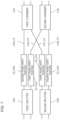
- FIG. 2 is a diagram illustrating an example of an optical 90-degree hybrid 8 according to the embodiment.
- FIG. 3 is a diagram for describing operations of the optical 90-degree hybrid 8 .
- FIG. 4 is a cross-sectional view taken along line IV, XII-IV, XII in FIG. 2 .
- the optical 90-degree hybrid 8 includes a first splitter 10 a that has a first output port Pout 1 and a second output port Pout 2 .
- the first splitter 10 a is a 2 ⁇ 2 multimode interferometer, for example.
- the term “2 ⁇ 2 multimode interferometer” will be abbreviated to “2 ⁇ 2 MMI” hereinafter.
- the second output port Pout 2 is, for example, a through port to an input port PA to which a later-described first input light 16 a (see FIG. 3 ) enters (i.e., an output port facing the input port PA).
- the first output port Pout 1 is, for example, a cross-port with respect to the input port PA (i.e., another output port that is separate from the through port).
- the optical 90-degree hybrid 8 further includes a second splitter 10 b that has a third output port Pout 3 and a fourth output port Pout 4 .
- the second splitter 10 b is a 2 ⁇ 2 MMI, for example.
- the fourth output port Pout 4 is, for example, a through port to an input port PB to which a later-described second input light 16 b enters (i.e., an output port facing the input port PB).
- the third output port Pout 3 is, for example, a cross-port with respect to the input port PB.
- the optical 90-degree hybrid 8 further includes a first combiner 12 a that has a first input port Pin 1 and a second input port Pin 2 .
- the first combiner 12 a is a 2 ⁇ 2 MMI, for example.
- the optical 90-degree hybrid 8 further includes a second combiner 12 b that has a third input port Pin 3 and a fourth input port Pin 4 .
- the second combiner 12 b is a 2 ⁇ 2 MMI, for example.
- the optical 90-degree hybrid 8 further includes a first arm waveguide 14 a that connects the first output port Pout 1 and the third input port Pin 3 .
- the optical 90-degree hybrid 8 further includes a second arm waveguide 14 b that connects the second output port Pout 2 and the second input port Pin 2 .
- the optical 90-degree hybrid 8 further includes a third arm waveguide 14 c that connects the third output port Pout 3 and the first input port Pin 1 .
- the optical 90-degree hybrid 8 further includes a fourth arm waveguide 14 d that connects the fourth output port Pout 4 and the fourth input port Pin 4 .
- the first to fourth arm waveguides 14 a , 14 b , 14 c , and 14 d are channel waveguides, for example.
- the first splitter 10 a splits a first light 16 a (hereinafter referred to as first input light) into a first split light 18 a and a second split light 18 b , outputs the first split light 18 a from the first output port Pout 1 , and outputs the second split light 18 b from the second output port Pout 2 .
- the first split light 18 a and the second split light 18 b are lights obtained by the above splitting of the first input light 16 a .
- the first input light 16 a is a reference light LO, for example.
- the second splitter 10 b splits a second light 16 b (hereinafter referred to as second input light) into a third split light 18 c and a fourth split light 18 d , outputs the third split light 18 c from the third output port Pout 3 , and outputs the fourth split light 18 d from the fourth output port Pout 4 .
- the third split light 18 c and the fourth split light 18 d are lights obtained by the above splitting of the second input light 16 b .
- the second input light 16 b is a signal light S, for example.
- the first combiner 12 a combines the second split light 18 b that enters thereto via the second arm waveguide 14 b and the third split light 18 c that enters thereto via the third arm waveguide 14 c so as to generate a first interference light IF 1 and a second interference light IF 2 .
- the first combiner 12 a outputs the first interference light IF 1 , which is generated, and the second interference light IF 2 , which also is generated.
- the second interference light IF 2 is an interference light that is opposite in phase to the first interference light IF 1 .
- the first interference light IF 1 and the second interference light IF 2 are lights generated by interference between the second split light 18 b and the third split light 18 c .
- the first interference light IF 1 is the interference light In described with reference to FIG. 1 .
- the second interference light IF 2 is the interference light Ip described with reference to FIG. 1 .
- the second combiner 12 b combines the fourth split light 18 d that enters thereto via the fourth arm waveguide 14 d and the first split light 18 a that enters thereto via the first arm waveguide 14 a so as to generate a third interference light IF 3 and a fourth interference light IF 4 .
- the second combiner 12 b outputs the third interference light IF 3 , which is generated, and the fourth interference light IF 4 , which also is generated.
- the fourth interference light IF 4 is an interference light that is opposite in phase to the third interference light IF 3 .
- the third interference light IF 3 and the fourth interference light IF 4 are lights generated by interference between the fourth split light 18 d and the first split light 18 a .
- the third interference light IF 3 is the interference light Qn described with reference to FIG. 1 .
- the fourth interference light IF 4 is the interference light Qp described with reference to FIG. 1 .
- Each of the first and second splitters 10 a and 10 b , the first to fourth arm waveguides 14 a , 14 b , 14 c , and 14 d , and the first and second combiners 12 a and 12 b is a part of an optical waveguide 24 that has a core 20 (see FIG. 4 ) and cladding 22 that surrounds the core 20 .
- the cladding 22 is a member that has a lower refractive index than that of the core 20 .
- the optical waveguide 24 is an optical element that is configured to satisfy the following Expressions (1) to (7) in a case in which a wavelength ⁇ is a certain wavelength and X is zero.
- the variable X is deviation of a structural parameter (e.g., width W of the core 20 ) from a first value (e.g., design value). This case (i.e., the wavelength ⁇ is a certain wavelength and X is zero) will be referred to as “optimal conditions” hereinafter.
- ⁇ is the wavelength of the first input light 16 a and the second input light 16 b (the same hereinafter).
- Structure parameter is a parameter based on the size of a cross-section of the core 20 , or the shape of this cross-section. This “cross-section” is a cross-section perpendicular to the travelling direction (in other words, path) of a light propagated through the core 20 (see FIG. 4 ).
- a parameter based on the “size of a cross-section of the core” is, for example, dimensions of the core 20 (e.g., width W of the core 20 or thickness T of the core 20 ).
- a parameter based on the “shape of this cross-section” is, for example, an angle between a side wall and a bottom face of the core 20 (i.e., sidewall angle).
- the width W of the core 20 is a dimension of the above “cross-section” (i.e., a cross-section perpendicular to the travelling direction of a light propagated through the core 20 ), and is a dimension in a direction H parallel to a substrate Sub on which the optical waveguide 24 is disposed.
- the thickness T of the core 20 is a dimension of the above “cross-section”, and is a dimension in a direction V perpendicular to the substrate Sub on which the optical waveguide 24 is disposed.
- the “first value” is, for example, a design value used in manufacturing the optical 90-degree hybrid 8 (i.e., a target value for a structural parameter that is obtained as a result of the design of the optical 90-degree hybrid 8 ).
- the above “deviation” is, for example, manufacturing error.
- the manufacturing error is, for example, a difference between a design value A of the width W (or the thickness T) of the core 20 and an actual value B of the width W (or the thickness T) of the core 20 , the difference being B minus A. In many cases, the manufacturing error is nearly constant irrespective of the position in the element.
- a value x of the structural parameter is a value obtained by adding deviation X to the above “first value” X 0 .
- the actual value of the structural parameter for the optical waveguide 24 is a value (e.g., 1.161 ⁇ m) obtained by adding a certain deviation (e.g., manufacturing error 25 nm) to the first value X 0 (e.g., design value 1.136 ⁇ m).
- the certain deviation can be a variety of values. (e.g., ⁇ 25 nm, 0 nm, +25 nm, etc.).
- the “first value” X 0 changes along each path of the first input light 16 a , the second input light 16 b , and the first to fourth split lights 18 a , 18 b , 18 c , and 18 d .
- the first value X 0 e.g., design value
- the first value X 0 for core width of the first splitter 10 a is greater than the first value X 0 (e.g., design value) for core width of the first arm waveguide 14 a .
- the “core width” means the width of the core.
- ⁇ 1 is a difference obtained by subtracting a second phase Ph 2 of the electric field of the second split light 18 b from a first phase Ph 1 of the electric field of the first split light 18 a (i.e., Ph 1 minus Ph 2 ).
- the first phase Ph 1 is the phase at the first output port Pout 1 .
- the second phase Ph 2 is the phase at the second output port Pout 2 .
- ⁇ 2 is a difference obtained by subtracting a fourth phase Ph 4 of the electric field of the fourth split light 18 d from a third phase Ph 3 of the electric field of the third split light 18 c (i.e., Ph 3 minus Ph 4 ).
- the third phase Ph 3 is the phase at the third output port Pout 3 .
- the fourth phase Ph 4 is the phase at the fourth output port Pout 4 .
- ⁇ is a phase imparted by Expression (8).
- ⁇ 1 is a phase imparted to the first split light 18 a by the first arm waveguide 14 a (i.e., the change amount generated in the phase of the first split light 18 a due to the first split light 18 a passing through the first arm waveguide 14 a , hereinafter the same).
- ⁇ 2 is a phase imparted to the second split light 18 b by the second arm waveguide 14 b .
- ⁇ 3 is a phase imparted to the third split light 18 c by the third arm waveguide 14 c .
- ⁇ 4 is a phase imparted to the fourth split light 18 d by the fourth arm waveguide 14 d .
- m is an integer.
- k is either +1 or ⁇ 1.
- the unit of phases is radian, unless specified otherwise (hereinafter the same). Note that the above “phase” does not include ⁇ t (where ⁇ is angular frequency of light, and t
- ⁇ 1 and ⁇ 2 , and ⁇ 1 to ⁇ 4 are functions of ⁇ and X. Note that ⁇ 1 and ⁇ 2 , and ⁇ 1 to ⁇ 4 are functions obtained in a case in which the wavelength of the first input light 16 a and the wavelength of the second input light 16 b are coincident with each other.
- the first combiner 12 a and the second combiner 12 b are supposed to be 2 ⁇ 2 MMIs having the same configuration in the following description. However, the conclusion described below will be unchanged even when the first combiner 12 a and the second combiner 12 b are not 2 ⁇ 2 MMIs having the same configuration.
- the first combiner 12 a is an optical element configured to output the first interference light IF 1 , and the second interference light IF 2 that is opposite in phase to the first interference light IF 1 .
- the second combiner 12 b is an optical element configured to output the third interference light IF 3 , and the fourth interference light IF 4 that is opposite in phase to the third interference light IF 3 .
- Expression (12) represents the total derivative ⁇ ( ⁇ ) of the phase error ⁇ .
- ⁇ is the change amount (i.e., amount of change) of ⁇ .
- ⁇ X is the change amount of X.
- the coefficient of ⁇ a in Expression (12) is the sum of a partial derivative of ⁇ as to ⁇ and a partial derivative of ⁇ 1 + ⁇ 2 as to ⁇ .
- ⁇ is the certain wavelength and deviation X is zero (i.e., the aforementioned “optimal conditions”)
- partial derivative of ⁇ as to ⁇ and a partial derivative of ⁇ 1 + ⁇ 2 as to ⁇ are of opposite signs from each other, which can be understood from Expressions (1) to (3).
- ⁇ is the above “certain wavelength” and deviation X is zero
- the coefficient of ⁇ in Expression (12) becomes small. The same can be said for the coefficient of ⁇ X in Expression (12).
- phase error ⁇ due to the deviation X e.g., manufacturing error
- the absolute value of deviation X increasing can be suppressed, while suppressing change in the phase error ⁇ due to change in the wavelength ⁇ (i.e., wavelength dependency of phase error).
- ⁇ is the above “certain wavelength” and the deviation X is zero
- the coefficient of ⁇ and the coefficient of ⁇ X can be easily made to be zero (see “(4) Arm Waveguide”).
- the first and second splitters 10 a and 10 b are realized by 2 ⁇ 2 MMIs, for example, as exemplified in “(2) Structure and Operations”. Description will thus be made here that the first and second splitters 10 a and 10 b realized by 2 ⁇ 2 MMIs satisfy Expressions (1), (2), (4), and (5).
- the ⁇ 1 of the first splitter 10 a realized by a 2 ⁇ 2 MMI is approximately ⁇ /2.
- the ⁇ 2 of the second splitter 10 b realized by another 2 ⁇ 2 MMI is also approximately ⁇ /2. Accordingly, deviation ⁇ 1 ′ of ⁇ 1 from ⁇ /2, and deviation ⁇ 2 ′ of ⁇ 2 from ⁇ /2 can be used to rewrite Expression (11) as follows.
- FIG. 5 is a diagram illustrating an example of the relation between ⁇ 1 ′+ ⁇ 2 ′ and the wavelength ⁇ (i.e., the wavelength of the first and second input lights 16 a and 16 b ).
- FIG. 5 is a graph calculated by simulation.
- the first splitter 10 a and the second splitter 10 b are supposed to be 2 ⁇ 2 MMIs having the same structure.
- the vertical axis is ⁇ 1 ′+ ⁇ 2 ′.
- the horizontal axis is the wavelength ⁇ .
- the range of the horizontal axis is a broad range (1.525 to 1.57 ⁇ m), including the C-band (the same is true for FIGS. 9 to 11 ).
- ⁇ 1 ′+ ⁇ 2 ′ is a portion of the phase error ⁇ , the portion occurring in the splitters 10 (i.e., first and second splitters 10 a and 10 b ).
- FIG. 6 is a plan view of the 2 ⁇ 2 MMIs used for the simulation. These 2 ⁇ 2 MMIs are channel waveguides each of which has a core made of silicon (Si) and a cladding made of silicon dioxide (SiO 2 ). The thickness of the core 20 is 220 nm. The modes of the first input light 16 a and the second input light 16 b are supposed to be TE 0 . The dimensions of each part of the core 20 are illustrated in FIG. 6 .
- a solid line 26 in FIG. 5 is a graph obtained in a case in which the deviation X (e.g., manufacturing error) of the width W of the core 20 is 0 nm. This graph indicates the relation between ⁇ 1 ′+ ⁇ 2 ′ and the wavelength ⁇ (the same hereinafter).
- a dashed line 28 is a graph obtained in a case in which the deviation X of the width W of the core 20 is 25 nm.
- a chain line 30 is a graph obtained in a case in which the deviation X of the width W of the core 20 is ⁇ 25 nm.
- ⁇ 1 ′+ ⁇ 2 ′ is 0° at wavelength ⁇ 0 near the center wavelength 1.5475 ⁇ m on the horizontal axis, as indicated by the solid line 26 .
- the sign of the partial derivative of ⁇ 1 ′+ ⁇ 2 ′ with respect to the wavelength ⁇ is positive, as indicated by the solid line 26 .
- the 2 ⁇ 2 MMI that realizes the first splitter 10 a and the 2 ⁇ 2 MMI that realizes the second splitter 10 b have the same structure, as described earlier, and accordingly ⁇ 1 ′ and ⁇ 2 ′ are coincident with each other.
- the first and second splitters 10 a and 10 b satisfy Expression (1) concerning the partial derivative of ⁇ 1 and Expression (2) concerning the partial derivative of ⁇ 2 .
- the 2 ⁇ 2 MMIs can realize the splitters 10 (i.e., first and second splitters 10 a and 10 b ) that satisfy Expressions (1), (2), (4), and (5) in a case in which ⁇ is the certain wavelength ⁇ 0 and the deviation X is 0.
- Expressions (1), (2), (4), and (5) are satisfied over a broad range in which ⁇ is no less than 1.525 nm to no more than 1.57 nm and the deviation X is no less than ⁇ 25 nm to no more than 25 nm.
- the partial derivative of ⁇ 1 ′ with respect to the wavelength ⁇ becomes a value other than zero.
- the partial derivative of ⁇ 2 ′ with respect to the wavelength ⁇ as well. That is to say, ⁇ 1 ′ and ⁇ 2 ′ have wavelength dependency. Furthermore, ⁇ 1 ′ and ⁇ 2 ′ increase along with the wavelength ⁇ , as illustrated in FIG. 5 . Thus, ⁇ 1 ′ and ⁇ 2 ′ satisfy Expressions (1) and (2).
- n r is the effective refractive index of the MMI.
- W e is the effective core width of the MMI, and ⁇ is the wavelength of a light that is inputted into the MMI.
- Expression (14) can be readily obtained from Expressions (6) and (19) in Lucas. B. Sodano and Erik C. M. Pennings, “Optical Multi-Mode Interference Devices Based on Self-Imaging”, JOURNAL OF LIGHTWAVE TECHNOLOGY, vol. 13, no. 4, April 1995, pp. 615-627.
- the constant p in the Expression (19) is set to be 1 for obtaining the above Expression (14).
- the loss becomes minimal, and also the phase difference between the waveguide modes that are emitted from the output ports becomes almost exactly ⁇ /2. That is to say, ⁇ 1 ′ and ⁇ 2 ′ become almost exactly zero. Accordingly, the ⁇ that satisfies Expression (14) (hereinafter referred to as “zero phase-difference wavelength”) is a wavelength at which ⁇ 1 ′ and ⁇ 2 ′ become almost exactly zero.
- the deviation X in the above description is the deviation of the width W of the core.
- the same conclusion is reached for other deviation X (e.g., manufacturing error in thickness T of the core or manufacturing error in sidewall angle of the core) as well.
- TE 0 mode has an electric field parallel to the width direction of the core, and thus is readily affected by manufacturing error in the width direction of the core.
- TM 0 mode has an electric field parallel to the thickness direction of the core, and thus is readily affected by manufacturing error in the thickness direction of the core.
- the first to fourth arm waveguides 14 are realized by channel waveguides that have phase shift portions (see Japanese Laid-open Patent Publication No. 2021-148965), for example. Description will be made here that the first to fourth arm waveguides 14 that are realized by channel waveguides with phase shift portions satisfy Expressions (3) and (6).
- FIG. 7 is a diagram for describing the first to fourth arm waveguides 14 that have phase shift portions 32 .
- Each of the phase shift portions 32 is a part of an arm waveguides (e.g., the first arm waveguide 14 a ), and imparts this arm waveguide 14 with an optical path length that is different from that of another arm waveguide 14 (e.g., the second arm waveguide 14 b ).
- the other portion of the arm waveguide 14 i.e., the portion other than the phase shift portion
- the non-phase-shift portion of a certain arm waveguide 14 (e.g., the first arm waveguide 14 a ) has the same optical path length as that of each non-phase-shift portion of all other waveguides 14 (e.g., the second to fourth arm waveguides 14 b , 14 c , and 14 d ).
- FIG. 8 is a plan view of a core 34 of an i′th (where i is an integer of 1 to 4, hereinafter the same) phase shift portion 32 .
- the i′th phase shift portion 32 is, for example, a channel waveguide that has a width Wi and a length Li, as illustrated in FIG. 8 .
- the core 34 is a part of the core 20 of the optical waveguide 24 described with reference to FIG. 4 .
- Expression (15) is an expression illustrating the phase (Di that the i′th arm waveguide (e.g., the first arm waveguide 14 a ) imparts to the i′th split light (e.g., the first split light 18 a ).
- ⁇ 0 is the phase that the non-phase-shift portion of each arm waveguide 14 (e.g., the first arm waveguide 14 a ) imparts to the split light propagated through that arm waveguide (e.g., the first split light 18 a ).
- N eff ( ⁇ , W i ) is the effective refractive index of the split light propagated through the i′th phase shift portion 32 . This N eff ( ⁇ , W i ) is a function of the wavelength ⁇ and the width W i of the core 34 .
- N eff ( ⁇ , W i ) can be calculated by the finite element method, for example.
- N eff ( ⁇ , W i ) is calculated on the basis of the size (e.g., width or thickness) and shape (e.g., sidewall angle) of the cross-section of the core 34 , the material refractive index of the core 34 , and the material refractive index of the cladding surrounding the core 34 .
- FIG. 9 is a diagram illustrating an example of the relation between ⁇ obtained by Expression (16), and the wavelength ⁇ .
- FIG. 9 is a graph calculated by simulation.
- the vertical axis is ⁇ /2.
- the horizontal axis is the wavelength ⁇ .
- ⁇ /2 is a part of the phase error ⁇ , and the part is generated at the first to fourth arm waveguides 14 a , 14 b , 14 c , and 14 d.
- the arm waveguides 14 used for the simulation in FIG. 9 are channel waveguides that have the cores made of Si and the cladding made of 902 .
- the cores of these arm waveguides 14 have the same thickness as those of the cores of the 2 ⁇ 2 MMIs used for the simulation in FIG. 5 (i.e., 220 nm).
- the modes of the lights propagated through the arm waveguides 14 are supposed to be the modes used in the simulation in FIG. 5 (i.e., TE 0 ).
- a plurality of expressions (17) indicates the dimensions of the phase shift portions 32 used for the simulation. [Math. 25]
- Wi and Li in Expressions (17) are values obtained by a genetic algorithm so as to minimize the worst value (i.e., greatest value) of
- ⁇ is calculated on the basis of Expression (11), Expression (16), and the relation between ⁇ 1 ′+ ⁇ 2 ′ and the wavelength ⁇ , illustrated in FIG. 5 .
- ⁇ 0 is the wavelength described in “(3) Splitter”.
- the range of minimizing worst values is a range that satisfies 1.525 ⁇ m 1.57 ⁇ m and also ⁇ 25 nm ⁇ X ⁇ 25 nm.
- a solid line 36 in FIG. 9 is a graph obtained in a case in which the deviation X (e.g., manufacturing error) of the width Wi (see FIG. 8 ) of each phase shift portion is 0 nm.
- a dashed line 38 is a graph obtained in a case in which the deviation X of the width Wi of each phase shift portion is 25 nm.
- a chain line 40 is a graph obtained in a case in which the deviation X of the width Wi of each phase shift portion is ⁇ 25 nm.
- the arm waveguides 14 that satisfy Expressions (3) and (6) in a case in which ⁇ is the certain wavelength ⁇ 0 and deviation X is 0 can be realized by the channel waveguides having the phase shift portions, the deviation X being the manufacturing error of the core width here.
- Expressions (3) and (6) are satisfied over a broad range in which ⁇ is no less than 1.525 nm to no more than 1.57 nm and deviation X is no less than ⁇ 25 nm to no more than 25 nm.
- Expression (3) indicates the wavelength dependency that ⁇ satisfies. The reason why the arm waveguides 14 that have the phase shift portions 32 can satisfy Expression (3) will be described.
- partial differentiation by A is performed for the rightmost expression in Expression (16), obtaining the partial derivative of ⁇ with respect to ⁇ (i.e., the left side of Expression (3)).
- Expression (18) is obtained by this partial differentiation.
- This “electric field” means the electric field of light propagated through the core (the same hereinafter).
- the more the wavelength ⁇ increases the more strongly the effective refractive index of the core is affected by the material refractive index of the cladding.
- the material refractive index of the cladding is lower than the material refractive index of the core. Accordingly, the more the wavelength ⁇ increases, the more the effective refractive index of the core decreases.
- the partial derivative of the effective refractive index N eff ( ⁇ , W 1 ) with respect to the wavelength ⁇ is negative.
- the partial derivative of the effective refractive index N eff ( ⁇ , W 2 ) with respect to the wavelength ⁇ is also negative.
- Expression (6) indicates the manufacturing error (i.e., an example of deviation X) dependency that ⁇ satisfies. The reason why the arm waveguides 14 that have the phase shift portions 32 can satisfy Expression (6) will be described.
- Expression (16) is an expression obtained by this partial differentiation.
- the deviation w is a form of the deviation X.
- the deviation of the width W of the core will be expressed by “w” in the description relating to Expression (20), to avoid confusion.
- the material refractive index of the core is higher than the material refractive index of the cladding, and accordingly, the more the deviation w (i.e., the change amount of the width W) increases, the more the effective refractive index of the core increases.
- the partial derivative of the effective refractive index N eff ( ⁇ , W 1 ) with respect to the deviation w is positive.
- the partial derivative of the effective refractive index N eff ( ⁇ , W 2 ) with respect to the deviation w is positive.
- core cross-sectional area The greater the cross-sectional area of the core (hereinafter referred to as core cross-sectional area) is, and the more the electric field is concentrated in the core. Thus, the greater the core cross-sectional area is, the less electric field additionally leaks out from the core. Accordingly, the greater the core cross-sectional area is, the smaller the increase in effective refractive index due to the increase in the core cross-sectional area is.
- Expression (21) holds in a case in which the phase shift portions 32 satisfy W 1 ⁇ W 2 .
- the phase shift portions 32 further satisfy L 2 /L 1 ⁇ 1
- the partial derivative of ⁇ with respect to w i.e., the left side of Expression (20)
- the deviation w is a form of the deviation X of the structural parameter, and accordingly Expression (6) holds when L 2 /L 1 ⁇ 1 holds. Note however, that there are cases in which Expression (6) holds even without L 2 /L 1 ⁇ 1 holding.
- W 1 ⁇ W 2 and L 2 /L 1 ⁇ 1 are the same as the condition for Expression (3) to hold (see “Wavelength Dependency of ⁇ ”).
- FIG. 10 is a diagram illustrating an example of the relation between the phase error ⁇ (see Expression (13)) and the wavelength ⁇ .
- the vertical axis is the phase error ⁇ .
- the horizontal axis is the wavelength ⁇ .
- FIG. 10 is a graph calculated by simulation.
- the splitters 10 used for the simulation are the 2 ⁇ 2 MMIs used for the simulation in FIG. 5 .
- the arm waveguides 14 (see FIG. 7 ) used for the simulation are the channel waveguides used for the simulation in FIG. 9 .
- a solid line 42 in FIG. 10 is a graph obtained in a case in which the deviation X (e.g., manufacturing error) of the core width of each splitter 10 and each arm waveguide 14 is 0 nm.
- a dashed line 44 is a graph obtained in a case in which this deviation X is 25 nm.
- a chain line 46 is a graph obtained in a case in which this deviation X is ⁇ 25 nm.
- the phase error ⁇ is approximately zero over a broad wavelength range on the horizontal axis (1.525 ⁇ m to 1.57 ⁇ m), as indicated by the solid line 42 . Further, even in a case in which the deviation X of the core width is ⁇ 25 nm, the phase error ⁇ in the wavelength range indicated by the horizontal axis is ⁇ 0.72° at the most, as indicated by the dashed line 44 and the chain line 46 . This value is sufficiently smaller than the permissible range of variation for the phase error ⁇ of the optical 90-degree hybrid, the permissible range being ⁇ 5°.
- phase error ⁇ (more accurately, increase in absolute value of ⁇ ) due to the deviation X of the structural parameter increasing (more accurately, the absolute value of the deviation X increasing) can be suppressed, while suppressing increase in the phase error ⁇ (more accurately, increase in absolute value of ⁇ ) due to change in wavelength.
- an example of the deviation X is manufacturing error.
- FIG. 11 is a diagram illustrating an example of the relation between the phase error ⁇ and the wavelength ⁇ for an optical 90-degree hybrid in which the first and second splitters 10 a and 10 b are 1 ⁇ 2 MMIs.
- the vertical axis is the phase error ⁇ .
- the horizontal axis is the wavelength ⁇ .
- a solid line 48 in FIG. 11 is a graph obtained in a case in which the deviation X of the core width is 0 nm.
- a dashed line 50 is a graph obtained in a case in which the deviation X of the core width is 25 nm.
- a chain line 52 is a graph obtained in a case in which the deviation X of the core width is ⁇ 25 nm.
- the phase error ⁇ is approximately zero over a broad wavelength range on the horizontal axis (1.525 ⁇ m to 1.57 ⁇ m), as indicated by solid line 48 .
- the deviation X e.g., manufacturing error
- phase error ⁇ of ⁇ 2.7° occurs, as indicated by the dashed line 50 .
- phase error ⁇ of 2.8° occurs, as indicated by the chain line 52 .
- the reason is that the first and second splitters 10 a and 10 b that are formed of 1 ⁇ 2 MMIs do not satisfy Expressions (4) and (5).
- the optical 90-degree hybrid 8 is used in a quadrature phase-shift keying (QPSK) receiver, for example.
- QPSK quadrature phase-shift keying
- the reference light LO is inputted to the first splitter 10 a (see FIG. 3 ), and phase-modulated signal light S is inputted to the second splitter 10 b .
- the reference light LO is a light that has approximately the same wavelength as that of the signal light S.
- the phase of the signal light S is modulated at four values of which intervals are 90° (i.e., 0°, 90°, 180°, and 270°).
- the first splitter 10 a splits the reference light LO and inputs the splitted reference light LO into the first and second combiners 12 a and 12 b via the first and second arm waveguides 14 a and 14 b .
- the second splitter 10 b splits the signal light S and inputs the splitted signal light S into the first and second combiners 12 a and 12 b via the third and fourth arm waveguides 14 c and 14 d .
- the first and second combiners 12 a and 12 b each mix the splitted reference light LO and the splitted signal light S, and output the four interference lights In, Ip, Qn, and Qp with phase intervals of 90°.
- the interference light In and the interference light Ip are inputted to a balanced photodetector (omitted from illustration) and are converted into a first electrical signal.
- the interference light Qn and the interference light Qp are inputted to a different balanced photodetector (omitted from illustration) and are converted into a second electrical signal.
- Two orthogonal transmission signals are demodulated from the first and second electrical signals.
- the reference light LO is inputted to the first splitter 10 a and the signal light S is inputted to the second splitter 10 b in the above example.
- the signal light S may be inputted to the first splitter 10 a and the reference light LO is inputted to the second splitter 10 b as well.
- FIG. 12 is a diagram for describing an example of a manufacturing method of the optical 90-degree hybrid 8 according to the embodiment.
- FIG. 12 is a cross-sectional view taken along line IV, XII-IV, XII in FIG. 2 .
- the optical 90-degree hybrid 8 has the core 20 and the cladding 22 surrounding the core, as described with reference to FIG. 4 .
- the cladding 22 has, for example, a lower cladding layer 54 and an upper cladding layer 56 .
- an upper-portion Si layer of a silicon on insulator (SOI) wafer is partially etched, so that the core 20 is formed. Further, a SiO 2 film is deposited on the SOI wafter that has the formed core 20 , thereby forming the upper cladding layer 56 .
- the optical 90-degree hybrid 8 is formed by the above processes.
- the lower cladding layer 54 is a buried oxide (BOX) layer of the SOI wafer.
- FIG. 13 is a plan view of a modification 108 of the optical 90-degree hybrid 8 .
- the structure of the modification 108 is similar to that of the optical 90-degree hybrid 8 described with reference to FIGS. 2 and 3 . Accordingly, description of portions that are in common with those of the optical 90-degree hybrid 8 will be omitted or simplified.
- the optical 90-degree hybrid 8 described with reference to FIGS. 2 and 3 has the first and third arm waveguides 14 a and 14 c that cross each other (see FIG. 3 ).
- the modification 108 has four arm waveguides 114 that are bent at 90° at its middle. Split lights of the first input light 16 a and split lights of the second input light 16 b are inputted to the first and second combiners 12 a and 12 b by these four arm waveguides 114 in the modification 108 .
- the arm waveguides 114 do not cross each other, and accordingly occurrence of crossing loss (i.e., loss occurring at a crossing portion of optical waveguides) can be avoided. Further, according to the modification 108 , crosstalk can be avoided from occurring at the crossing portion of the arm waveguides.
- Forming the cores of the arm waveguides 114 of Si (or SiN) and forming the cladding of SiO 2 yields a larger relative refractive index difference between the cladding and the cores, and accordingly the curvature radius of the bent portions of the arm waveguides 114 can be made smaller.
- Such a configuration enables propagation loss at the arm waveguides 114 to be further suppressed, since reduction in size of the arm waveguides 114 is facilitated.
- the optical 90-degree hybrid 8 is configured such that phase error ( ⁇ 1 ′+ ⁇ 2 ′) occurring at the splitters 10 is cancelled out by the phase error ( ⁇ /2) occurring at the arm waveguides, as described with reference to FIGS. 2 to 10 .
- phase error ⁇ more accurately, increase in absolute value of ⁇
- increase in phase error ⁇ due to increase in deviation in structural parameters (more accurately, increase in absolute value of deviation) can be suppressed, while suppressing increase in the phase error ⁇ (more accurately, increase in absolute value of ⁇ ) due to wavelength change.
- the first and second splitters 10 a and 10 b may be optical elements other than 2 ⁇ 2 MMIs.
- the first and second splitters 10 a and 10 b may be a splitter disclosed in Weijie Chang, et al., “Inverse design and demonstration of an ultracompact broadband dual-mode 3 dB power splitter”, Optics Express, Vol. 26, No. 18, 2018, pp. 24135-24144, for example, which discloses a splitter in which wavelength dependance of loss is controllable by providing a plurality of holes in the core. This splitter also enables control of phase among the output ports.
- Each of the phase shift portions 32 is a linear waveguide that has a core with constant width.
- each of the phase shift portions 32 may be an optical waveguide other than a linear waveguide.
- each of the phase shift portions 32 may be a tapered optical waveguide that has a core of which the width gradually increases or decreases.
- the optical waveguide 24 is an optical waveguide based on silicon photonics.
- the optical waveguide 24 may be an optical waveguide based on a technology other than silicon photonics.
- the optical waveguide 24 may be an optical waveguide based on a planar lightwave circuit (PLC) in which both the core 20 and the cladding 22 are formed of SiO 2 .
- the optical waveguide 24 may be an indium phosphide (InP) waveguide or a gallium arsenide (GaAs) waveguide.
- the optical waveguide 24 may be an optical waveguide of which the core 20 is made of SiN.
- the lower cladding layer 54 is made of SiO 2 , for example, and the upper cladding layer 56 is made of SiO 2 or air.
- the optical waveguide 24 may be an optical waveguide from which the upper cladding layer 56 is omitted in the optical waveguide described with reference to FIG. 12 (i.e., an optical waveguide in which the upper cladding layer 56 is formed of air).
- the optical waveguide 24 is a channel waveguide.
- the optical waveguide 24 may be an optical waveguide other than a channel waveguide.
- the optical waveguide 24 may be any one of a rib waveguide, a high-mesa waveguide, and a ridge waveguide.
- the arm waveguides 14 cross at one location. However, the arm waveguides 14 may cross at a plurality of locations. Such a configuration enables the arm waveguides 14 to be made shorter, and thus loss at the arm waveguides 14 can be reduced.
- the deviation X is manufacturing error in the embodiment.
- the deviation X does not have to be manufacturing error.
- the arm waveguides 14 and so forth may be designed such that the phase error ⁇ is a value other than zero (e.g., 0.05°) in a case in which the structural parameter takes a design value and ⁇ is a certain wavelength ⁇ 0 .
- the deviation X is not manufacturing error, but deviation from a structural parameter value (i.e., a value of the structural parameter) with respect to which the phase error ⁇ becomes zero at the certain wavelength ⁇ 0 .
Landscapes
- Physics & Mathematics (AREA)
- General Physics & Mathematics (AREA)
- Optics & Photonics (AREA)
- Nonlinear Science (AREA)
- Engineering & Computer Science (AREA)
- Microelectronics & Electronic Packaging (AREA)
- Electromagnetism (AREA)
- Computer Networks & Wireless Communication (AREA)
- Signal Processing (AREA)
- Optical Integrated Circuits (AREA)
- Optical Modulation, Optical Deflection, Nonlinear Optics, Optical Demodulation, Optical Logic Elements (AREA)
Abstract
Description
[Math. 17]
ΔP={(Φ2−Φ3)−(Φ1−Φ4)}−(ϵ1+ϵ2) (9)
[Math. 25]
W1=W3=1.136 μm, L1=L3=3.903 μm
W2=W4=1.184 μm, L2=L4=3.825 μm (17)
Claims (4)
Applications Claiming Priority (2)
| Application Number | Priority Date | Filing Date | Title |
|---|---|---|---|
| JP2021-214827 | 2021-12-28 | ||
| JP2021214827A JP7741384B2 (en) | 2021-12-28 | 2021-12-28 | Optical 90-degree hybrid |
Publications (2)
| Publication Number | Publication Date |
|---|---|
| US20230208529A1 US20230208529A1 (en) | 2023-06-29 |
| US12184338B2 true US12184338B2 (en) | 2024-12-31 |
Family
ID=86896353
Family Applications (1)
| Application Number | Title | Priority Date | Filing Date |
|---|---|---|---|
| US17/991,263 Active 2042-12-17 US12184338B2 (en) | 2021-12-28 | 2022-11-21 | Optical 90-degree hybrid |
Country Status (3)
| Country | Link |
|---|---|
| US (1) | US12184338B2 (en) |
| JP (1) | JP7741384B2 (en) |
| CN (1) | CN116360034B (en) |
Citations (8)
| Publication number | Priority date | Publication date | Assignee | Title |
|---|---|---|---|---|
| JP2011018002A (en) | 2009-07-10 | 2011-01-27 | Nippon Telegr & Teleph Corp <Ntt> | 90° optical hybrid circuit |
| WO2011010469A1 (en) | 2009-07-22 | 2011-01-27 | 日本電信電話株式会社 | Optical 90-degree hybrid circuit |
| US20120237154A1 (en) * | 2011-03-18 | 2012-09-20 | Fujitsu Limited | Optical hybrid circuit and optical receiver |
| US8401351B2 (en) * | 2009-09-04 | 2013-03-19 | Furukawa Electric Co., Ltd. | 90-degree hybrid |
| US20200096699A1 (en) * | 2017-07-25 | 2020-03-26 | Elenion Technologies, Llc | Optical hybrid |
| US10731383B2 (en) | 2018-08-01 | 2020-08-04 | Macom Technology Solutions Holdings, Inc. | Symmetric coherent optical mixer |
| JP2020177109A (en) | 2019-04-17 | 2020-10-29 | 日本電信電話株式会社 | 90 degree light hybrid circuit |
| US20210294038A1 (en) * | 2020-03-19 | 2021-09-23 | Fujitsu Optical Components Limited | 90-degree optical hybrid |
Family Cites Families (8)
| Publication number | Priority date | Publication date | Assignee | Title |
|---|---|---|---|---|
| JP5202015B2 (en) | 2008-02-13 | 2013-06-05 | 日本電信電話株式会社 | Optical 90-degree hybrid function correction method, optical 90-degree hybrid function correction apparatus, and optical 90-degree hybrid function correction program |
| EP2367034A1 (en) * | 2010-03-16 | 2011-09-21 | Telefonaktiebolaget L M Ericsson (Publ) | Planar waveguide circuit comprising a 90 degree optical hybrid and optical receiver |
| WO2012086846A1 (en) * | 2010-12-21 | 2012-06-28 | 日本電気株式会社 | Optical waveguide device, and manufacturing method for optical waveguide device |
| JP5561304B2 (en) | 2012-03-30 | 2014-07-30 | 沖電気工業株式会社 | Optical element |
| JP6572175B2 (en) | 2016-06-27 | 2019-09-04 | 日本電信電話株式会社 | Waveguide type optical coupler |
| CN109445025A (en) * | 2018-12-19 | 2019-03-08 | 武汉邮电科学研究院有限公司 | A kind of modification method and structure of optical mixer unit phase error |
| CN210348114U (en) | 2019-05-08 | 2020-04-17 | 深圳新飞通光电子技术有限公司 | Free space polarized optical isolation component and free space type coherent receiver thereof |
| JP7380329B2 (en) | 2020-02-28 | 2023-11-15 | 富士通オプティカルコンポーネンツ株式会社 | Optical circuit devices and optical receivers |
-
2021
- 2021-12-28 JP JP2021214827A patent/JP7741384B2/en active Active
-
2022
- 2022-11-21 US US17/991,263 patent/US12184338B2/en active Active
- 2022-11-25 CN CN202211487567.7A patent/CN116360034B/en active Active
Patent Citations (11)
| Publication number | Priority date | Publication date | Assignee | Title |
|---|---|---|---|---|
| JP2011018002A (en) | 2009-07-10 | 2011-01-27 | Nippon Telegr & Teleph Corp <Ntt> | 90° optical hybrid circuit |
| WO2011010469A1 (en) | 2009-07-22 | 2011-01-27 | 日本電信電話株式会社 | Optical 90-degree hybrid circuit |
| US20120141067A1 (en) | 2009-07-22 | 2012-06-07 | Nippon Telegraph And Telephone Corporation | Optical 90-degree hybrid circuit |
| US8401351B2 (en) * | 2009-09-04 | 2013-03-19 | Furukawa Electric Co., Ltd. | 90-degree hybrid |
| US20120237154A1 (en) * | 2011-03-18 | 2012-09-20 | Fujitsu Limited | Optical hybrid circuit and optical receiver |
| US20200096699A1 (en) * | 2017-07-25 | 2020-03-26 | Elenion Technologies, Llc | Optical hybrid |
| US10731383B2 (en) | 2018-08-01 | 2020-08-04 | Macom Technology Solutions Holdings, Inc. | Symmetric coherent optical mixer |
| JP2020177109A (en) | 2019-04-17 | 2020-10-29 | 日本電信電話株式会社 | 90 degree light hybrid circuit |
| US20220171127A1 (en) * | 2019-04-17 | 2022-06-02 | Nippon Telegraph And Telephone Corporation | Optical 90 Degree Hybrid Circuit |
| US20210294038A1 (en) * | 2020-03-19 | 2021-09-23 | Fujitsu Optical Components Limited | 90-degree optical hybrid |
| JP2021148965A (en) | 2020-03-19 | 2021-09-27 | 富士通オプティカルコンポーネンツ株式会社 | 90-degree optical hybrid |
Non-Patent Citations (2)
| Title |
|---|
| Chang, W. et al., "Inverse design and demonstration of an ultracompact broadband dual-mode 3 dB power splitter", Optics Express 24135, vol. 26, No. 18, Sep. 3, 2018 (10 pp.). |
| Soldano, L. et al., "Optical Multi-Mode Interference Devices Based on Self-Imaging: Principles and Applications", IEEE, Journal of Lightwave Technology, vol. 13, No. 4, Apr. 1995, pp. 615-627. |
Also Published As
| Publication number | Publication date |
|---|---|
| JP2023098205A (en) | 2023-07-10 |
| CN116360034B (en) | 2026-04-21 |
| US20230208529A1 (en) | 2023-06-29 |
| CN116360034A (en) | 2023-06-30 |
| JP7741384B2 (en) | 2025-09-18 |
Similar Documents
| Publication | Publication Date | Title |
|---|---|---|
| US11402581B2 (en) | Mode converter | |
| US9465168B2 (en) | Polarization beam splitter and optical device | |
| Jeong et al. | Novel Optical 90 ^∘ Hybrid Consisting of a Paired Interference Based 2 \,*\, 4 MMI Coupler, a Phase Shifter and a 2 \,*\, 2 MMI Coupler | |
| JP5966021B2 (en) | Polarization conversion element | |
| US8280256B2 (en) | Optical hybrid circuit, optical receiver and light receiving method | |
| US8744222B2 (en) | Practical silicon photonic multi-function integrated-optic chip for fiber sensor applications | |
| US7826689B2 (en) | Optical device which outputs independently modulated light beams in respective TE and TM polarization modes | |
| US8649643B2 (en) | Optical hybrid circuit and optical receiver | |
| US20170179680A1 (en) | Surface coupled systems | |
| US11223425B2 (en) | Optical circuit device, and optical receiver | |
| US9459406B2 (en) | Polarization beam splitter and optical device | |
| US8718412B2 (en) | Dual polarization quadrature phase shift keying optical modulator | |
| KR100943847B1 (en) | Waveguide Wideband Optical Isolator | |
| US11307355B2 (en) | 90-degree optical hybrid | |
| US20110064360A1 (en) | Optical semiconductor element and method for manufacturing the same | |
| US12085752B2 (en) | Optical waveguide device and optical integrated circuit that includes optical waveguide device | |
| US12184338B2 (en) | Optical 90-degree hybrid | |
| WO2017169922A1 (en) | Polarization beam splitter | |
| Romero-García et al. | Broadband, temperature tolerant and passively biased resonantly enhanced Mach-Zehnder modulators | |
| EP4207514A1 (en) | Silicon photonic symmetric distributed feedback laser | |
| CN112711146A (en) | Lithium niobate optical isolator with wavelength tuning function | |
| US9971225B2 (en) | Spot size converter, semiconductor optical device | |
| JP2019219484A (en) | Polarization cleaner and optical module |
Legal Events
| Date | Code | Title | Description |
|---|---|---|---|
| AS | Assignment |
Owner name: FUJITSU OPTICAL COMPONENTS LIMITED, JAPAN Free format text: ASSIGNMENT OF ASSIGNORS INTEREST;ASSIGNOR:OKA, AKIRA;REEL/FRAME:061842/0618 Effective date: 20221014 |
|
| FEPP | Fee payment procedure |
Free format text: ENTITY STATUS SET TO UNDISCOUNTED (ORIGINAL EVENT CODE: BIG.); ENTITY STATUS OF PATENT OWNER: LARGE ENTITY |
|
| STPP | Information on status: patent application and granting procedure in general |
Free format text: DOCKETED NEW CASE - READY FOR EXAMINATION |
|
| STPP | Information on status: patent application and granting procedure in general |
Free format text: NON FINAL ACTION MAILED |
|
| STPP | Information on status: patent application and granting procedure in general |
Free format text: RESPONSE TO NON-FINAL OFFICE ACTION ENTERED AND FORWARDED TO EXAMINER |
|
| STPP | Information on status: patent application and granting procedure in general |
Free format text: NOTICE OF ALLOWANCE MAILED -- APPLICATION RECEIVED IN OFFICE OF PUBLICATIONS |
|
| STPP | Information on status: patent application and granting procedure in general |
Free format text: PUBLICATIONS -- ISSUE FEE PAYMENT VERIFIED |
|
| STCF | Information on status: patent grant |
Free format text: PATENTED CASE |