US12178123B2 - Organic electroluminescence device and compound for organic electroluminescence device - Google Patents
Organic electroluminescence device and compound for organic electroluminescence device Download PDFInfo
- Publication number
- US12178123B2 US12178123B2 US17/179,837 US202117179837A US12178123B2 US 12178123 B2 US12178123 B2 US 12178123B2 US 202117179837 A US202117179837 A US 202117179837A US 12178123 B2 US12178123 B2 US 12178123B2
- Authority
- US
- United States
- Prior art keywords
- formula
- substituted
- group
- unsubstituted
- carbon atoms
- Prior art date
- Legal status (The legal status is an assumption and is not a legal conclusion. Google has not performed a legal analysis and makes no representation as to the accuracy of the status listed.)
- Active, expires
Links
Images


Classifications
-
- H—ELECTRICITY
- H10—SEMICONDUCTOR DEVICES; ELECTRIC SOLID-STATE DEVICES NOT OTHERWISE PROVIDED FOR
- H10K—ORGANIC ELECTRIC SOLID-STATE DEVICES
- H10K85/00—Organic materials used in the body or electrodes of devices covered by this subclass
- H10K85/60—Organic compounds having low molecular weight
- H10K85/649—Aromatic compounds comprising a hetero atom
- H10K85/657—Polycyclic condensed heteroaromatic hydrocarbons
-
- C—CHEMISTRY; METALLURGY
- C07—ORGANIC CHEMISTRY
- C07F—ACYCLIC, CARBOCYCLIC OR HETEROCYCLIC COMPOUNDS CONTAINING ELEMENTS OTHER THAN CARBON, HYDROGEN, HALOGEN, OXYGEN, NITROGEN, SULFUR, SELENIUM OR TELLURIUM
- C07F7/00—Compounds containing elements of Groups 4 or 14 of the Periodic Table
- C07F7/02—Silicon compounds
- C07F7/08—Compounds having one or more C—Si linkages
- C07F7/0803—Compounds with Si-C or Si-Si linkages
- C07F7/081—Compounds with Si-C or Si-Si linkages comprising at least one atom selected from the elements N, O, halogen, S, Se or Te
- C07F7/0812—Compounds with Si-C or Si-Si linkages comprising at least one atom selected from the elements N, O, halogen, S, Se or Te comprising a heterocyclic ring
- C07F7/0816—Compounds with Si-C or Si-Si linkages comprising at least one atom selected from the elements N, O, halogen, S, Se or Te comprising a heterocyclic ring said ring comprising Si as a ring atom
-
- C—CHEMISTRY; METALLURGY
- C07—ORGANIC CHEMISTRY
- C07F—ACYCLIC, CARBOCYCLIC OR HETEROCYCLIC COMPOUNDS CONTAINING ELEMENTS OTHER THAN CARBON, HYDROGEN, HALOGEN, OXYGEN, NITROGEN, SULFUR, SELENIUM OR TELLURIUM
- C07F5/00—Compounds containing elements of Groups 3 or 13 of the Periodic Table
- C07F5/02—Boron compounds
- C07F5/027—Organoboranes and organoborohydrides
-
- C—CHEMISTRY; METALLURGY
- C07—ORGANIC CHEMISTRY
- C07F—ACYCLIC, CARBOCYCLIC OR HETEROCYCLIC COMPOUNDS CONTAINING ELEMENTS OTHER THAN CARBON, HYDROGEN, HALOGEN, OXYGEN, NITROGEN, SULFUR, SELENIUM OR TELLURIUM
- C07F7/00—Compounds containing elements of Groups 4 or 14 of the Periodic Table
- C07F7/02—Silicon compounds
- C07F7/08—Compounds having one or more C—Si linkages
- C07F7/0803—Compounds with Si-C or Si-Si linkages
- C07F7/0805—Compounds with Si-C or Si-Si linkages comprising only Si, C or H atoms
-
- C—CHEMISTRY; METALLURGY
- C09—DYES; PAINTS; POLISHES; NATURAL RESINS; ADHESIVES; COMPOSITIONS NOT OTHERWISE PROVIDED FOR; APPLICATIONS OF MATERIALS NOT OTHERWISE PROVIDED FOR
- C09K—MATERIALS FOR MISCELLANEOUS APPLICATIONS, NOT PROVIDED FOR ELSEWHERE
- C09K11/00—Luminescent materials, e.g. electroluminescent or chemiluminescent
- C09K11/06—Luminescent materials, e.g. electroluminescent or chemiluminescent containing organic luminescent materials
-
- H—ELECTRICITY
- H10—SEMICONDUCTOR DEVICES; ELECTRIC SOLID-STATE DEVICES NOT OTHERWISE PROVIDED FOR
- H10K—ORGANIC ELECTRIC SOLID-STATE DEVICES
- H10K50/00—Organic light-emitting devices
- H10K50/10—OLEDs or polymer light-emitting diodes [PLED]
- H10K50/11—OLEDs or polymer light-emitting diodes [PLED] characterised by the electroluminescent [EL] layers
- H10K50/12—OLEDs or polymer light-emitting diodes [PLED] characterised by the electroluminescent [EL] layers comprising dopants
-
- H—ELECTRICITY
- H10—SEMICONDUCTOR DEVICES; ELECTRIC SOLID-STATE DEVICES NOT OTHERWISE PROVIDED FOR
- H10K—ORGANIC ELECTRIC SOLID-STATE DEVICES
- H10K50/00—Organic light-emitting devices
- H10K50/80—Constructional details
- H10K50/84—Passivation; Containers; Encapsulations
- H10K50/844—Encapsulations
-
- H—ELECTRICITY
- H10—SEMICONDUCTOR DEVICES; ELECTRIC SOLID-STATE DEVICES NOT OTHERWISE PROVIDED FOR
- H10K—ORGANIC ELECTRIC SOLID-STATE DEVICES
- H10K85/00—Organic materials used in the body or electrodes of devices covered by this subclass
- H10K85/40—Organosilicon compounds, e.g. TIPS pentacene
-
- H—ELECTRICITY
- H10—SEMICONDUCTOR DEVICES; ELECTRIC SOLID-STATE DEVICES NOT OTHERWISE PROVIDED FOR
- H10K—ORGANIC ELECTRIC SOLID-STATE DEVICES
- H10K85/00—Organic materials used in the body or electrodes of devices covered by this subclass
- H10K85/60—Organic compounds having low molecular weight
- H10K85/615—Polycyclic condensed aromatic hydrocarbons, e.g. anthracene
- H10K85/622—Polycyclic condensed aromatic hydrocarbons, e.g. anthracene containing four rings, e.g. pyrene
-
- H—ELECTRICITY
- H10—SEMICONDUCTOR DEVICES; ELECTRIC SOLID-STATE DEVICES NOT OTHERWISE PROVIDED FOR
- H10K—ORGANIC ELECTRIC SOLID-STATE DEVICES
- H10K85/00—Organic materials used in the body or electrodes of devices covered by this subclass
- H10K85/60—Organic compounds having low molecular weight
- H10K85/615—Polycyclic condensed aromatic hydrocarbons, e.g. anthracene
- H10K85/623—Polycyclic condensed aromatic hydrocarbons, e.g. anthracene containing five rings, e.g. pentacene
-
- H—ELECTRICITY
- H10—SEMICONDUCTOR DEVICES; ELECTRIC SOLID-STATE DEVICES NOT OTHERWISE PROVIDED FOR
- H10K—ORGANIC ELECTRIC SOLID-STATE DEVICES
- H10K85/00—Organic materials used in the body or electrodes of devices covered by this subclass
- H10K85/60—Organic compounds having low molecular weight
- H10K85/631—Amine compounds having at least two aryl rest on at least one amine-nitrogen atom, e.g. triphenylamine
- H10K85/636—Amine compounds having at least two aryl rest on at least one amine-nitrogen atom, e.g. triphenylamine comprising heteroaromatic hydrocarbons as substituents on the nitrogen atom
-
- H—ELECTRICITY
- H10—SEMICONDUCTOR DEVICES; ELECTRIC SOLID-STATE DEVICES NOT OTHERWISE PROVIDED FOR
- H10K—ORGANIC ELECTRIC SOLID-STATE DEVICES
- H10K85/00—Organic materials used in the body or electrodes of devices covered by this subclass
- H10K85/60—Organic compounds having low molecular weight
- H10K85/649—Aromatic compounds comprising a hetero atom
- H10K85/654—Aromatic compounds comprising a hetero atom comprising only nitrogen as heteroatom
-
- H—ELECTRICITY
- H10—SEMICONDUCTOR DEVICES; ELECTRIC SOLID-STATE DEVICES NOT OTHERWISE PROVIDED FOR
- H10K—ORGANIC ELECTRIC SOLID-STATE DEVICES
- H10K85/00—Organic materials used in the body or electrodes of devices covered by this subclass
- H10K85/60—Organic compounds having low molecular weight
- H10K85/649—Aromatic compounds comprising a hetero atom
- H10K85/656—Aromatic compounds comprising a hetero atom comprising two or more different heteroatoms per ring
-
- H—ELECTRICITY
- H10—SEMICONDUCTOR DEVICES; ELECTRIC SOLID-STATE DEVICES NOT OTHERWISE PROVIDED FOR
- H10K—ORGANIC ELECTRIC SOLID-STATE DEVICES
- H10K85/00—Organic materials used in the body or electrodes of devices covered by this subclass
- H10K85/60—Organic compounds having low molecular weight
- H10K85/649—Aromatic compounds comprising a hetero atom
- H10K85/657—Polycyclic condensed heteroaromatic hydrocarbons
- H10K85/6572—Polycyclic condensed heteroaromatic hydrocarbons comprising only nitrogen in the heteroaromatic polycondensed ring system, e.g. phenanthroline or carbazole
-
- H—ELECTRICITY
- H10—SEMICONDUCTOR DEVICES; ELECTRIC SOLID-STATE DEVICES NOT OTHERWISE PROVIDED FOR
- H10K—ORGANIC ELECTRIC SOLID-STATE DEVICES
- H10K85/00—Organic materials used in the body or electrodes of devices covered by this subclass
- H10K85/60—Organic compounds having low molecular weight
- H10K85/649—Aromatic compounds comprising a hetero atom
- H10K85/657—Polycyclic condensed heteroaromatic hydrocarbons
- H10K85/6574—Polycyclic condensed heteroaromatic hydrocarbons comprising only oxygen in the heteroaromatic polycondensed ring system, e.g. cumarine dyes
-
- H—ELECTRICITY
- H10—SEMICONDUCTOR DEVICES; ELECTRIC SOLID-STATE DEVICES NOT OTHERWISE PROVIDED FOR
- H10K—ORGANIC ELECTRIC SOLID-STATE DEVICES
- H10K85/00—Organic materials used in the body or electrodes of devices covered by this subclass
- H10K85/60—Organic compounds having low molecular weight
- H10K85/649—Aromatic compounds comprising a hetero atom
- H10K85/657—Polycyclic condensed heteroaromatic hydrocarbons
- H10K85/6576—Polycyclic condensed heteroaromatic hydrocarbons comprising only sulfur in the heteroaromatic polycondensed ring system, e.g. benzothiophene
-
- H—ELECTRICITY
- H10—SEMICONDUCTOR DEVICES; ELECTRIC SOLID-STATE DEVICES NOT OTHERWISE PROVIDED FOR
- H10K—ORGANIC ELECTRIC SOLID-STATE DEVICES
- H10K85/00—Organic materials used in the body or electrodes of devices covered by this subclass
- H10K85/60—Organic compounds having low molecular weight
- H10K85/658—Organoboranes
-
- C—CHEMISTRY; METALLURGY
- C09—DYES; PAINTS; POLISHES; NATURAL RESINS; ADHESIVES; COMPOSITIONS NOT OTHERWISE PROVIDED FOR; APPLICATIONS OF MATERIALS NOT OTHERWISE PROVIDED FOR
- C09K—MATERIALS FOR MISCELLANEOUS APPLICATIONS, NOT PROVIDED FOR ELSEWHERE
- C09K2211/00—Chemical nature of organic luminescent or tenebrescent compounds
- C09K2211/10—Non-macromolecular compounds
- C09K2211/1003—Carbocyclic compounds
- C09K2211/1007—Non-condensed systems
-
- C—CHEMISTRY; METALLURGY
- C09—DYES; PAINTS; POLISHES; NATURAL RESINS; ADHESIVES; COMPOSITIONS NOT OTHERWISE PROVIDED FOR; APPLICATIONS OF MATERIALS NOT OTHERWISE PROVIDED FOR
- C09K—MATERIALS FOR MISCELLANEOUS APPLICATIONS, NOT PROVIDED FOR ELSEWHERE
- C09K2211/00—Chemical nature of organic luminescent or tenebrescent compounds
- C09K2211/10—Non-macromolecular compounds
- C09K2211/1003—Carbocyclic compounds
- C09K2211/1011—Condensed systems
-
- C—CHEMISTRY; METALLURGY
- C09—DYES; PAINTS; POLISHES; NATURAL RESINS; ADHESIVES; COMPOSITIONS NOT OTHERWISE PROVIDED FOR; APPLICATIONS OF MATERIALS NOT OTHERWISE PROVIDED FOR
- C09K—MATERIALS FOR MISCELLANEOUS APPLICATIONS, NOT PROVIDED FOR ELSEWHERE
- C09K2211/00—Chemical nature of organic luminescent or tenebrescent compounds
- C09K2211/10—Non-macromolecular compounds
- C09K2211/1003—Carbocyclic compounds
- C09K2211/1014—Carbocyclic compounds bridged by heteroatoms, e.g. N, P, Si or B
-
- C—CHEMISTRY; METALLURGY
- C09—DYES; PAINTS; POLISHES; NATURAL RESINS; ADHESIVES; COMPOSITIONS NOT OTHERWISE PROVIDED FOR; APPLICATIONS OF MATERIALS NOT OTHERWISE PROVIDED FOR
- C09K—MATERIALS FOR MISCELLANEOUS APPLICATIONS, NOT PROVIDED FOR ELSEWHERE
- C09K2211/00—Chemical nature of organic luminescent or tenebrescent compounds
- C09K2211/10—Non-macromolecular compounds
- C09K2211/1018—Heterocyclic compounds
- C09K2211/1025—Heterocyclic compounds characterised by ligands
- C09K2211/1029—Heterocyclic compounds characterised by ligands containing one nitrogen atom as the heteroatom
- C09K2211/104—Heterocyclic compounds characterised by ligands containing one nitrogen atom as the heteroatom with other heteroatoms
-
- C—CHEMISTRY; METALLURGY
- C09—DYES; PAINTS; POLISHES; NATURAL RESINS; ADHESIVES; COMPOSITIONS NOT OTHERWISE PROVIDED FOR; APPLICATIONS OF MATERIALS NOT OTHERWISE PROVIDED FOR
- C09K—MATERIALS FOR MISCELLANEOUS APPLICATIONS, NOT PROVIDED FOR ELSEWHERE
- C09K2211/00—Chemical nature of organic luminescent or tenebrescent compounds
- C09K2211/10—Non-macromolecular compounds
- C09K2211/1018—Heterocyclic compounds
- C09K2211/1025—Heterocyclic compounds characterised by ligands
- C09K2211/1044—Heterocyclic compounds characterised by ligands containing two nitrogen atoms as heteroatoms
- C09K2211/1055—Heterocyclic compounds characterised by ligands containing two nitrogen atoms as heteroatoms with other heteroatoms
-
- C—CHEMISTRY; METALLURGY
- C09—DYES; PAINTS; POLISHES; NATURAL RESINS; ADHESIVES; COMPOSITIONS NOT OTHERWISE PROVIDED FOR; APPLICATIONS OF MATERIALS NOT OTHERWISE PROVIDED FOR
- C09K—MATERIALS FOR MISCELLANEOUS APPLICATIONS, NOT PROVIDED FOR ELSEWHERE
- C09K2211/00—Chemical nature of organic luminescent or tenebrescent compounds
- C09K2211/10—Non-macromolecular compounds
- C09K2211/1018—Heterocyclic compounds
- C09K2211/1025—Heterocyclic compounds characterised by ligands
- C09K2211/1059—Heterocyclic compounds characterised by ligands containing three nitrogen atoms as heteroatoms
-
- C—CHEMISTRY; METALLURGY
- C09—DYES; PAINTS; POLISHES; NATURAL RESINS; ADHESIVES; COMPOSITIONS NOT OTHERWISE PROVIDED FOR; APPLICATIONS OF MATERIALS NOT OTHERWISE PROVIDED FOR
- C09K—MATERIALS FOR MISCELLANEOUS APPLICATIONS, NOT PROVIDED FOR ELSEWHERE
- C09K2211/00—Chemical nature of organic luminescent or tenebrescent compounds
- C09K2211/10—Non-macromolecular compounds
- C09K2211/1018—Heterocyclic compounds
- C09K2211/1025—Heterocyclic compounds characterised by ligands
- C09K2211/1088—Heterocyclic compounds characterised by ligands containing oxygen as the only heteroatom
-
- C—CHEMISTRY; METALLURGY
- C09—DYES; PAINTS; POLISHES; NATURAL RESINS; ADHESIVES; COMPOSITIONS NOT OTHERWISE PROVIDED FOR; APPLICATIONS OF MATERIALS NOT OTHERWISE PROVIDED FOR
- C09K—MATERIALS FOR MISCELLANEOUS APPLICATIONS, NOT PROVIDED FOR ELSEWHERE
- C09K2211/00—Chemical nature of organic luminescent or tenebrescent compounds
- C09K2211/10—Non-macromolecular compounds
- C09K2211/1018—Heterocyclic compounds
- C09K2211/1025—Heterocyclic compounds characterised by ligands
- C09K2211/1092—Heterocyclic compounds characterised by ligands containing sulfur as the only heteroatom
-
- C—CHEMISTRY; METALLURGY
- C09—DYES; PAINTS; POLISHES; NATURAL RESINS; ADHESIVES; COMPOSITIONS NOT OTHERWISE PROVIDED FOR; APPLICATIONS OF MATERIALS NOT OTHERWISE PROVIDED FOR
- C09K—MATERIALS FOR MISCELLANEOUS APPLICATIONS, NOT PROVIDED FOR ELSEWHERE
- C09K2211/00—Chemical nature of organic luminescent or tenebrescent compounds
- C09K2211/10—Non-macromolecular compounds
- C09K2211/1018—Heterocyclic compounds
- C09K2211/1025—Heterocyclic compounds characterised by ligands
- C09K2211/1096—Heterocyclic compounds characterised by ligands containing other heteroatoms
-
- H—ELECTRICITY
- H10—SEMICONDUCTOR DEVICES; ELECTRIC SOLID-STATE DEVICES NOT OTHERWISE PROVIDED FOR
- H10K—ORGANIC ELECTRIC SOLID-STATE DEVICES
- H10K2101/00—Properties of the organic materials covered by group H10K85/00
- H10K2101/20—Delayed fluorescence emission
-
- H—ELECTRICITY
- H10—SEMICONDUCTOR DEVICES; ELECTRIC SOLID-STATE DEVICES NOT OTHERWISE PROVIDED FOR
- H10K—ORGANIC ELECTRIC SOLID-STATE DEVICES
- H10K50/00—Organic light-emitting devices
- H10K50/10—OLEDs or polymer light-emitting diodes [PLED]
- H10K50/11—OLEDs or polymer light-emitting diodes [PLED] characterised by the electroluminescent [EL] layers
-
- H—ELECTRICITY
- H10—SEMICONDUCTOR DEVICES; ELECTRIC SOLID-STATE DEVICES NOT OTHERWISE PROVIDED FOR
- H10K—ORGANIC ELECTRIC SOLID-STATE DEVICES
- H10K50/00—Organic light-emitting devices
- H10K50/80—Constructional details
- H10K50/85—Arrangements for extracting light from the devices
Definitions
- the disclosure relates to a compound used as a luminescence material and an organic electroluminescence device including the same.
- the organic electroluminescence display is a so-called self-luminescent display device in which holes and electrons injected from a first electrode and a second electrode recombine in an emission layer, and thus a luminescent material including an organic compound in the emission layer emits light to implement display.
- an organic electroluminescence device In the application of an organic electroluminescence device to a display device, there is a continuous demand for an organic electroluminescence device having a low driving voltage, high light emission efficiency, and a long service life, and for the development of materials for an organic electroluminescence device that is capable of stably attaining such characteristics.
- TTA triplet-triplet annihilation
- TADF thermally activated delayed fluorescence
- the disclosure provides an organic electroluminescence device exhibiting excellent light emission efficiency.
- the disclosure also provides a compound which is a material for an organic electroluminescence device emitting deep-blue light and having high efficiency characteristics.
- X 1 and X 2 may each independently be O or S, and at least one of L 1 to L 11 may be a substituent represented by Formula 2-a or Formula 2-b, the remainder of L 1 to L 11 may each independently be a hydrogen atom, a deuterium atom, a halogen atom, a cyano group, a substituted or unsubstituted amine group, a substituted or unsubstituted silyl group, a substituted or unsubstituted boron group, a substituted or unsubstituted linear or branched alkyl group having 1 to 20 carbon atoms, a substituted or unsubstituted aryl group having 6 to 30 ring-forming carbon atoms, or a substituted or unsubstituted heteroaryl group having 2 to 30 ring-forming carbon atoms.
- R 1 to R 24 may each independently be a hydrogen atom, a deuterium atom, a halogen atom, a cyano group, a substituted or unsubstituted amine group, a substituted or unsubstituted silyl group, a substituted or unsubstituted boron group, a substituted or unsubstituted alkyl group having 1 to 20 carbon atoms, a substituted or unsubstituted aryl group having 6 to 30 ring-forming carbon atoms, or a substituted or unsubstituted heteroaryl group having 2 to 30 ring-forming carbon atoms.
- Ar 1 and Ar 2 may each independently be a substituted or unsubstituted alkyl group having 1 to 20 carbon atoms, a substituted or unsubstituted aryl group having 6 to 30 ring-forming carbon atoms, or a substituted or unsubstituted heteroaryl group having 2 to 30 ring-forming carbon atoms
- Ar 3 may be a substituted or unsubstituted alkyl group having 1 to 20 carbon atoms, a substituted or unsubstituted aryl group having 6 to 30 ring-forming carbon atoms, a substituted or unsubstituted heteroaryl group having 2 to 30 ring-forming carbon atoms, or a substituent represented by Formula 1.
- L 1 to L 11 in Ar 3 may each independently be a hydrogen atom, a deuterium atom, a halogen atom, a cyano group, a substituted or unsubstituted amine group, a substituted or unsubstituted silyl group, a substituted or unsubstituted boron group, a substituted or unsubstituted linear or branched alkyl group having 1 to 20 carbon atoms, a substituted or unsubstituted aryl group having 6 to 30 ring-forming carbon atoms, or a substituted or unsubstituted heteroaryl group having 2 to 30 ring-forming carbon atoms.
- Formula 1 may be represented by one of Formula 1-1 to Formula 1-3:
- L 1 to L 11 may be the same as defined in Formula 1.
- Formula 1 may be represented by one of Formula 1A to Formula 1E:
- a to c may each independently be an integer from 0 to 3
- X 1 and X 2 may be the same as defined in Formula 1
- L a to L c and L 1 to L 11 may each independently be a hydrogen atom, a deuterium atom, a halogen atom, a cyano group, a substituted or unsubstituted amine group, a substituted or unsubstituted silyl group, a substituted or unsubstituted boron group, a substituted or unsubstituted linear or branched alkyl group having 1 to 20 carbon atoms, a substituted or unsubstituted aryl group having 6 to 30 ring-forming carbon atoms, or a substituted or unsubstituted heteroaryl group having 2 to 30 ring-forming carbon atoms, and DU may be represented by Formula 2-a or Formula 2-b.
- Formula 1 may be represented by Formula 1F:
- R 9 to R 24 may be the same as defined in Formula 2-b, AU may be a substituent represented by Formula 1, except that AU may not be substituted with a substituent represented by Formula 2-a or Formula 2-b.
- Formula 1 may be represented by one of Formula 1F-1 to Formula 1F-3:
- L 1 to L 11 may each independently be a hydrogen atom, a deuterium atom, a halogen atom, a cyano group, a substituted or unsubstituted amine group, a substituted or unsubstituted silyl group, a substituted or unsubstituted boron group, a substituted or unsubstituted linear or branched alkyl group having 1 to 20 carbon atoms, a substituted or unsubstituted aryl group having 6 to 30 ring-forming carbon atoms, or a substituted or unsubstituted heteroaryl group having 2 to 30 ring-forming carbon atoms, X 1 and X 2 may be the same as defined in Formula 1, and R 9 to R 24 may be the same as defined in Formula 2-b.
- At least one hydrogen atom may be substituted with a deuterium atom.
- Ar 1 and Ar 2 may each independently be an unsubstituted phenyl group, a phenyl group substituted with a deuterium atom, an unsubstituted biphenyl group, an unsubstituted naphthyl group, or an unsubstituted dibenzothiophene group.
- the compound represented by Formula 1 may be a blue luminescent material.
- the compound represented by Formula 1 may be a thermally activated delayed fluorescence emitting material.
- an organic electroluminescence device including a first electrode, a second electrode disposed on the first electrode, and an emission layer disposed between the first electrode and the second electrode.
- the emission layer may include a compound represented by Formula 1.
- the organic electroluminescence device may further include a capping layer disposed on the second electrode, and the capping layer may have a refractive index of greater than or equal to about 1.6.
- the emission layer may be a delayed fluorescence emission layer containing a host and a dopant, and the dopant may include the compound represented by Formula 1.
- the emission layer may emit blue light having a center wavelength in a range of about 430 nm to about 490 nm.
- FIG. 1 is a schematic cross-sectional view illustrating an organic electroluminescence device according to an embodiment of the inventive concept.
- FIG. 2 is a schematic cross-sectional view illustrating an organic electroluminescence device according to an embodiment of the inventive concept.
- FIG. 3 is a schematic cross-sectional view illustrating an organic electroluminescence device according to an embodiment of the inventive concept.
- FIG. 4 is a schematic cross-sectional view illustrating an organic electroluminescence device according to an embodiment of the inventive concept.
- inventive concept may have various modifications and may be embodied in different forms, and example embodiments will be explained in detail with reference to the accompanying drawings.
- inventive concept may, however, be embodied in different forms and should not be construed as limited to the embodiments set forth herein. Rather, all modifications, equivalents, and substituents which are included in the spirit and technical scope of the inventive concept should be included in the inventive concept.
- the term “and/or” includes any and all combinations of one or more of the associated listed items.
- “A and/or B” may be understood to mean “A, B, or A and B.”
- the terms “and” and “or” may be used in the conjunctive or disjunctive sense and may be understood to be equivalent to “and/or”.
- the expression “at least one of A, B, and C” may indicate only A, only B, only C, both A and B, both A and C, both B and C, all of A, B, and C, or variations thereof.
- At least one of is intended to include the meaning of “at least one selected from” for the purpose of its meaning and interpretation. For example, “at least one of A and B” may be understood to mean “A, B, or A and B.” When preceding a list of elements, the term, “at least one of,” modifies the entire list of elements and does not modify the individual elements of the list.
- FIGS. 1 to 4 are schematic cross-sectional views illustrating organic electroluminescence devices according to embodiments of the inventive concept.
- a first electrode EL1 and a second electrode EL2 are disposed to face each other and an emission layer EML may be disposed between the first electrode EL1 and the second electrode EL2.
- Each of the organic electroluminescence devices 10 of the embodiments may further include functional layers between the first electrode EL1 and the second electrode EL2 in addition to the emission layer EML.
- the functional layers may include a hole transport region HTR and an electron transport region ETR.
- each of the organic electroluminescence devices 10 according to embodiments may include the first electrode EL1, the hole transport region HTR, the emission layer EML, the electron transport region ETR, and the second electrode EL2 that may be sequentially stacked.
- the organic electroluminescence device 10 of an embodiment may include a capping layer CPL disposed on the second electrode EL2.
- the organic electroluminescence device 10 of an embodiment may include a compound according to an embodiment described below in the emission layer EML disposed between the first electrode EL1 and the second electrode EL2.
- the organic electroluminescence device 10 of an embodiment may include a compound according to an embodiment described below in the hole transport region HTR or the electron transport region ETR which is one of the functional layers disposed between the first electrode EL1 and the second electrode EL2, as well as in the emission layer EML.
- FIG. 2 illustrates a schematic cross-sectional view of an organic electroluminescence device 10 of an embodiment, in which a hole transport region HTR includes a hole injection layer HIL and a hole transport layer HTL, and an electron transport region ETR includes an electron injection layer EIL and an electron transport layer ETL.
- FIG. 3 illustrates a schematic cross-sectional view of an organic electroluminescence device 10 of an embodiment, in which a hole transport region HTR includes a hole injection layer HIL, a hole transport layer HTL, and an electron blocking layer EBL, and an electron transport region ETR includes an electron injection layer EIL, an electron transport layer ETL, and a hole blocking layer HBL.
- FIG. 4 illustrates a schematic cross-sectional view of an organic electroluminescence device 10 of an embodiment including a capping layer CPL disposed on the second electrode EL2.
- the first electrode EL1 has a conductivity.
- the first electrode EL1 may be formed of a metal alloy or a conductive compound.
- the first electrode EL1 may be an anode.
- the first electrode EL1 may be a pixel electrode.
- the first electrode EL1 may be a transmissive electrode, a transflective electrode, or a reflective electrode.
- the first electrode EL1 may include a transparent metal oxide, such as indium tin oxide (ITO), indium zinc oxide (IZO), zinc oxide (ZnO), and indium tin zinc oxide (ITZO).
- the first electrode EL1 When the first electrode EL1 is a transflective electrode or a reflective electrode, the first electrode EL1 may include Ag, Mg Cu, Al, Pt, Pd, Au, Ni, Nd, Ir, Cr, Li, Ca, LiF/Ca, LiF/Al, Mo, Ti, a compound thereof, or a mixture thereof (e.g., a mixture of Ag and Mg). In other embodiments, the first electrode EL1 may have a multilayer structure including a reflective layer or a transflective layer formed of the above-described materials, and a transparent conductive layer formed of ITO, IZO, ZnO, ITZO, etc.
- the first electrode EL1 may have a three-layer structure of ITO/Ag/ITO, but is not limited thereto.
- the thickness of the first electrode EL1 may be in a range of about 1,000 ⁇ to about 10,000 ⁇ .
- the thickness of the first electrode EL1 may be in a range of about 1,000 ⁇ to about 3,000 ⁇ .
- the hole transport region HTR may be provided on the first electrode EL1.
- the hole transport region HTR may include at least one of a hole injection layer HIL, a hole transport layer HTL, a hole buffer layer (not shown), or an electron blocking layer.
- the thickness of the hole transport region HTR may be, for example, in a range of about 50 ⁇ to about 15,000 ⁇ .
- the hole transport region HTR may have a single layer formed of a single material, a single layer formed of different materials, or a multilayer structure including layers formed of different materials.
- the hole transport region HTR may have a single layer structure of a hole injection layer HIL or a hole transport layer HTL, and may have a single layer structure formed of a hole injection material and a hole transport material.
- the hole transport region HTR may have a single layer structure formed of different materials, or it may have a structure in which a hole injection layer HIL/hole transport layer HTL, a hole injection layer HIL/hole transport layer HTL/hole buffer layer (not shown), a hole injection layer HIL/hole buffer layer (not shown), a hole transport layer HTL/hole buffer layer, or a hole injection layer HIL/hole transport layer HTL/electron blocking layer EBL are stacked in order from the first electrode EL1, but an embodiment is not limited thereto.
- the hole transport region HTR may be formed using various methods such as a vacuum deposition method, a spin coating method, a cast method, a Langmuir-Blodgett (LB) method, an inkjet printing method, a laser printing method, and a laser induced thermal imaging (LITI) method.
- a vacuum deposition method such as a vacuum deposition method, a spin coating method, a cast method, a Langmuir-Blodgett (LB) method, an inkjet printing method, a laser printing method, and a laser induced thermal imaging (LITI) method.
- LB Langmuir-Blodgett
- LITI laser induced thermal imaging
- the hole injection layer HIL may include, for example, a phthalocyanine compound such as copper phthalocyanine; N,N′-diphenyl-N,N′-bis-[4-(phenyl-m-tolyl-amino)-phenyl]-biphenyl-4,4′-diamine (DNTPD), 4,4′,4′′-[tris(3-methylphenyl)phenylamino]triphenylamine](m-MTDATA), 4,4′,4′′-tris(N,N-diphenylamino)triphenylamine (TDATA), 4,4′,4′′-tris ⁇ N,-(2-naphthyl)-N-phenylamino)-triphenylamine (2-TNATA), poly(3,4-ethylenedioxythiophene)/poly(4-styrenesulfonate) (PEDOT/PSS), polyaniline/dodecylbenzenesulfonic acid (P
- the hole transport layer HTL may include, for example, carbazole derivatives such as N-phenyl carbazole and polyvinyl carbazole, fluorene derivatives, N4,N4′-di(naphthalen-1-yl)-N4,N4′-diphenyl-[1,1′-biphenyl]-4,4′-diamine ( ⁇ -NPD), N,N′-bis(3-methylphenyl)-N,N′-diphenyl-[1,1-biphenyl]-4,4′-diamine (TPD), triphenylamine derivatives such as 4,4′,4′′-tris(N-carbazolyl)triphenylamine (TCTA), N,N′-di(naphthalenyl)-N,N′-diphenyl-benzidine (NPB), 4,4′-cyclohexylidene bis[N,N-bis(4-methylphenyl]benzenamine](TAPC), 4,4′-bis[
- the electron blocking layer EBL may include, for example, 9-phenyl-9H-3,9′-bicarbazole (CCP), 1,3-bis(N-carbazolyl)benzene (mCP), 1,3-bis(1,8-dimethyl-9H-carbazol-9-yl)benzene (mDCP), etc.
- CCP 9-phenyl-9H-3,9′-bicarbazole
- mCP 1,3-bis(N-carbazolyl)benzene
- mDCP 1,3-bis(1,8-dimethyl-9H-carbazol-9-yl)benzene
- the thickness of the hole transport region HTR may be in a range of about 50 ⁇ to about 10,000 ⁇ .
- the thickness of the hole transport region HTR may be in a range of about 100 ⁇ to about 5,000 ⁇ .
- the thickness of the hole injection layer HIL may be, for example, in a range of about 30 ⁇ to about 1,000 ⁇
- the thickness of the hole transport layer HTL may be in a range of about 30 ⁇ to about 1,000 ⁇ .
- the thickness of the electron blocking layer EBL may be in a range of about 10 ⁇ to about 1,000 ⁇ . If the thicknesses of the hole transport region HTR, the hole injection layer HIL, the hole transport layer HTL, and the electron blocking layer EBL satisfy the above-described ranges, satisfactory hole transport properties may be achieved without a substantial increase in driving voltage.
- the hole transport region HTR may further include a charge generating material to increase conductivity.
- the charge generating material may be dispersed uniformly or non-uniformly in the hole transport region HTR.
- the charge generating material may be, for example, a p-dopant.
- the p-dopant may be one of quinone derivatives, metal oxides, or cyano group-containing compounds, but is not limited thereto.
- non-limiting examples of the p-dopant may include, but are not limited to, quinone derivatives such as tetracyanoquinodimethane (TCNQ) and 2,3,5,6-tetrafluoro-7,7,8,8-tetracyanoquinodimethane (F4-TCNQ), metal oxides such as tungsten oxides and molybdenum oxides.
- quinone derivatives such as tetracyanoquinodimethane (TCNQ) and 2,3,5,6-tetrafluoro-7,7,8,8-tetracyanoquinodimethane (F4-TCNQ)
- metal oxides such as tungsten oxides and molybdenum oxides.
- the hole transport region HTR may further include at least one of a hole buffer layer (not shown) or an electron blocking layer EBL in addition to the hole injection layer HIL and the hole transport layer HTL.
- the hole buffer layer (not shown), may compensate a resonance distance according to the wavelength of light emitted from an emission layer EML and may increase light emission efficiency.
- Materials which may be included in the hole transport region HTR may be used as materials which may be included in the hole buffer layer (not shown).
- the electron blocking layer EBL is a layer that serves may serve to prevent electrons from being injected from the electron transport region ETR to the hole transport region HTR.
- the emission layer EML is provided on the hole transport region HTR.
- the thickness of the emission layer EML may be in a range of about 100 ⁇ to about 1000 ⁇ .
- the thickness of the emission layer EML may be in a range of about 100 ⁇ to about 300 ⁇ .
- the emission layer EML may have a single layer formed of a single material, a single layer formed of different materials, or a multilayer structure having layers formed of different materials.
- the emission layer EML in the organic electroluminescence device 10 of an embodiment may include a compound of an embodiment.
- the compound according to an embodiment may include at least one azasiline unit and at least one condensed cyclic unit containing a boron atom (B).
- the condensed cyclic unit may include two heteroatoms selected from among an oxygen atom (O) and a sulfur atom (S) in addition to the boron atom.
- the condensed cyclic unit may have a structure in which five hexacyclic rings are condensed, and the heteroatom may include a boron atom.
- the azasiline unit may include one azasiline moiety, or may have a spiro structure in which two azasiline moieties are bonded.
- the compound of an embodiment may include a condensed cyclic unit containing a boron atom as an electron acceptor, and an azasiline unit as an electron donor.
- the compound of an embodiment may have a structure in which at least one electron acceptor and at least one electron donor are bonded.
- the term “substituted or unsubstituted” may indicate that one is substituted or unsubstituted with at least one substituent selected from the group consisting of a deuterium atom, a halogen atom, a cyano group, a nitro group, an amino group, a silyl group, an oxy group, a thio group, a sulfinyl group, a sulfonyl group, a carbonyl group, a boryl group, a phosphine oxide group, a phosphine sulfide group, an alkyl group, an alkenyl group, an alkynyl group, an alkoxy group, a hydrocarbon ring group, an aryl group, and a heterocyclic group.
- a biphenyl group may be interpreted as an aryl group or a phenyl group
- examples of the halogen atom may include a fluorine atom, a chlorine atom, a bromine atom, and an iodine atom.
- the alkyl group may be a linear, branched or cyclic type.
- the number of carbons in the alkyl group is 1 to 50, 1 to 30, 1 to 20, 1 to 10, or 1 to 6.
- Examples of the alkyl group may include, but are not limited to, methyl group, ethyl group, n-propyl group, isopropyl group, n-butyl group, s-butyl group, t-butyl group, i-butyl group, 2-ethylbutyl group, 3,3-dimethylbutyl group, n-pentyl group, i-pentyl group, neopentyl group, t-pentyl group, cyclopentyl group, 1-methylpentyl group, 3-methylpentyl group, 2-ethylpentyl group, 4-methyl-2-pentyl group, n-hexyl group, 1-methylhexyl group, 2-ethylhexy
- an aryl group means any functional group or substituent derived from an aromatic hydrocarbon ring.
- the aryl group may be a monocyclic aryl group or a polycyclic aryl group.
- the number of ring-forming carbon atoms in the aryl group may be 6 to 30, 6 to 20, or 6 to 15.
- aryl group may include phenyl, naphthyl, fluorenyl, anthracenyl, phenanthryl, biphenyl, terphenyl, quaterphenyl, quinquephenyl, sexiphenyl, triphenylenyl, pyrenyl, benzofluoranthenyl, chrysenyl, etc., but are not limited thereto.
- the heteroaryl group may include at least one of B, O, N, P, Si, or S as a heteroatom.
- the heteroaryl group may contain two or more heteroatoms, the two or more heteroatoms may be the same as or different from each other.
- the heteroaryl group may be a monocyclic heteroaryl group or a polycyclic heteroaryl group.
- the number of ring-forming carbon atoms in the heteroaryl group may be 2 to 30, 2 to 20, or 2 to 10.
- heteroaryl group may include thiophene, furan, pyrrole, imidazole, thiazole, oxazole, oxadiazole, triazole, pyridyl, bipyridyl, pyrimidyl, triazine, triazole, acridyl, pyridazine, pyrazinyl, quinolinyl, quinazoline, quinoxalinyl, phenoxazyl, phthalazinyl, pyrido pyrimidyl, pyrido pyrazinyl, pyrazino pyrazinyl, isoquinoline, indole, carbazole, N-arylcarbazole, N-heteroarylcarbazole, N-alkylcarbazole, benzoxazole, benzoimidazole, benzothiazole, benzocarbazole, benzothiophene, dibenzothiophen
- the silyl group includes an alkyl silyl group and an aryl silyl group.
- Examples of the silyl group may include, but are not limited to, trimethylsilyl, triethylsilyl, t-butyldimethylsilyl, propyldimethylsilyl, triphenylsilyl, diphenylsilyl, phenylsilyl, etc.
- the number of carbon atoms in an amine group is not specifically limited, but may be 1 to 30.
- the amine group may include an alkyl amine group and an aryl amine group. Examples of the amine group may include, but are not limited to, methylamine group, dimethylamine group, phenylamine group, diphenylamine group, naphthylamine group, 9-methyl-anthracenylamine group, triphenylamine group, etc.
- the boron group includes an alkyl boron group and an aryl boron group.
- Examples of the boron group may include, but are not limited to, trimethylboron, triethylboron, t-butyldimethylboron, triphenylboron, diphenylboron, phenylboron, etc.
- the alkyl group in the alkylaryl group, the alkyl boron group, the alkyl silyl group, and the alkyl amine group is the same as examples of the alkyl group described above.
- the aryl group in the aryl boron group, the aryl silyl group, and the aryl amine group is the same as examples of the aryl group described above.
- the emission layer EML in the organic electroluminescence device 10 of an embodiment may include a compound represented by Formula 1.
- X 1 and X 2 may each independently be O or S.
- both X 1 and X 2 may be O
- both X 1 and X 2 may be S
- one among X 1 and X 2 may be O, and the other may be S.
- L 1 to L 11 may be a substituent represented by Formula 2-a or Formula 2-b.
- one selected from L 1 to L 11 , two selected from L 1 to L 11 , or three selected from L 1 to L 11 may be a substituent represented by Formula 2-a or Formula 2-b.
- L 1 to L 11 is a substituent represented by Formula 2-a or Formula 2-b
- the remainder of L 1 to L 11 may each independently be a hydrogen atom, a deuterium atom, a halogen atom, a cyano group, a substituted or unsubstituted amine group, a substituted or unsubstituted silyl group, a substituted or unsubstituted boron group, a substituted or unsubstituted linear or branched alkyl group having 1 to 20 carbon atoms, a substituted or unsubstituted aryl group having 6 to 30 ring-forming carbon atoms, or a substituted or unsubstituted heteroaryl group having 2 to 30 ring-forming carbon atoms.
- L 1 to L 11 in the case where one of L 1 to L 11 is a substituent represented by Formula 2-a or Formula 2-b, the remainder of L 1 to Ln may each independently be a hydrogen atom, a deuterium atom, a fluorine atom, a cyano group, an aryl amine group, an aryl silyl group, an aryl boron group, a linear alkyl group, a branched alkyl group, an unsubstituted aryl group, an aryl group substituted with a deuterium atom, or an unsubstituted heteroaryl group.
- the embodiments are not limited thereto.
- L 1 to L 11 are cyclic alkyl groups may be excluded.
- At least one of L 1 to L 11 may be represented by Formula 2-a or Formula 2-b:
- R 1 to R 24 may each independently be a hydrogen atom, a deuterium atom, a halogen atom, a cyano group, a substituted or unsubstituted amine group, a substituted or unsubstituted silyl group, a substituted or unsubstituted boron group, a substituted or unsubstituted alkyl group having 1 to 20 carbon atoms, a substituted or unsubstituted aryl group having 6 to 30 ring-forming carbon atoms, or a substituted or unsubstituted heteroaryl group having 2 to 30 ring-forming carbon atoms.
- R 1 to R 24 may each independently be a hydrogen atom, a deuterium atom, a fluorine atom, a cyano group, an aryl amine group, an aryl silyl group, an aryl boron group, a linear alkyl group, a branched alkyl group, an unsubstituted aryl group, an aryl group substituted with a deuterium atom, or an unsubstituted heteroaryl group, etc.
- the embodiments are not limited thereto.
- Ar 1 and Ar 2 may each independently be a substituted or unsubstituted alkyl group having 1 to 20 carbon atoms, a substituted or unsubstituted aryl group having 6 to 30 ring-forming carbon atoms, or a substituted or unsubstituted heteroaryl group having 2 to 30 ring-forming carbon atoms.
- Ar 1 and Ar 2 may each independently be an unsubstituted phenyl group, a phenyl group substituted with a deuterium atom, an unsubstituted biphenyl group, an unsubstituted naphthyl group, or an unsubstituted dibenzothiophene group.
- Ar 1 and Ar 2 may be the same as or different from each other. However, the embodiments are not limited thereto.
- Ar 3 is a substituted or unsubstituted alkyl group having 1 to 20 carbon atoms, a substituted or unsubstituted aryl group having 6 to 30 ring-forming carbon atoms, a substituted or unsubstituted heteroaryl group having 2 to 30 ring-forming carbon atoms, or a substituent represented by Formula 1.
- L 1 to L 11 in Ar 3 may each independently be a hydrogen atom, a deuterium atom, a halogen atom, a cyano group, a substituted or unsubstituted amine group, a substituted or unsubstituted silyl group, a substituted or unsubstituted boron group, a substituted or unsubstituted linear or branched alkyl group having 1 to 20 carbon atoms, a substituted or unsubstituted aryl group having 6 to 30 ring-forming carbon atoms, or a substituted or unsubstituted heteroaryl group having 2 to 30 ring-forming carbon atoms.
- Formula 2-b
- At least one hydrogen atom may be substituted with a deuterium atom.
- all the hydrogen atoms in the compound of an embodiment may be substituted with deuterium atoms.
- a substituent represented by Formula 2-a or Formula 2-b in the compound represented by Formula 1 of an embodiment may be excluded, and all the other hydrogen atoms may be substituted with deuterium atoms.
- all the hydrogen atoms in a substituent represented by Formula 2-a or Formula 2-b bonded to Formula 1 may be substituted with deuterium atoms.
- the compound represented by Formula 1 of an embodiment may be represented by one of Formula 1-1 to Formula 1-3.
- Formula 1-1 to Formula 1-3 represent examples according to the combination of heteroatoms contained in the condensed cyclic unit.
- the compound of an embodiment may include the condensed cyclic unit containing oxaborine or thiaborine as represented by Formula 1-1 to Formula 1-3 below:
- L 1 to L 11 may be the same as defined in Formula 1.
- the compound of an embodiment may include, as an electron acceptor, the condensed cyclic unit containing oxaborine or thiaborine.
- the compound represented by Formula 1 of an embodiment may be represented by one of Formula 1A to Formula 1E.
- DU may be represented by Formula 2-a or Formula 2-b as described above.
- Formula 1A to Formula 1E show embodiments according to the azasiline unit's bonding site represented by DU and the number of the bonded azasiline units.
- a to c may each independently be an integer from 0 to 3.
- X 1 and X 2 may be the same as defined in Formula 1.
- L a to L e and L 1 to L 11 may each independently be a hydrogen atom, a deuterium atom, a halogen atom, a cyano group, a substituted or unsubstituted amine group, a substituted or unsubstituted silyl group, a substituted or unsubstituted boron group, a substituted or unsubstituted linear or branched alkyl group having 1 to 20 carbon atoms, a substituted or unsubstituted aryl group having 6 to 30 ring-forming carbon atoms, or a substituted or unsubstituted heteroaryl group having 2 to 30 ring-forming carbon atoms.
- the compound represented by Formula 1A to Formula 1E of an embodiment the compound represented by Formula 1A to Formula 1E of an embodiment, the
- L a to L c and L 1 to L 11 may each independently be a hydrogen atom, a deuterium atom, a fluorine atom, a cyano group, an aryl amine group, an aryl silyl group, an aryl boron group, a linear alkyl group, a branched alkyl group, an unsubstituted aryl group, an aryl group substituted with a deuterium atom, or an unsubstituted heteroaryl group, etc.
- R 9 to R 24 may be the same as defined in Formula 2-b, AU is a substituent represented by Formula 1, and the case where AU is substituted with a substituent represented by Formula 2-a or Formula 2-b above is excluded. For example, AU is not substituted with a substituent represented by Formula 2-a or Formula 2-b.
- R 9 to R 24 may each independently be a hydrogen atom, a deuterium atom, a fluorine atom, a cyano group, an aryl amine group, an aryl silyl group, an aryl boron group, a linear alkyl group, a branched alkyl group, an unsubstituted aryl group, an aryl group substituted with a deuterium atom, or an unsubstituted heteroaryl group, etc.
- the embodiments are not limited thereto.
- Formula 1F shows an embodiment having a structure containing the azasiline unit represented by Formula 2-b and the condensed cyclic unit represented by Formula 1.
- the compound represented by Formula 1F of an embodiment may have a structure containing two electron acceptor units which may be represented by Formula 1 and one electron donor unit which may be represented by Formula 2-b.
- the compound represented by Formula 1 of an embodiment may be represented by one of Formula 1F-1 to Formula 1F-3.
- Formula 1F-1 to Formula 1F-3 show embodiments having a structure containing the azasiline unit represented by Formula 2-b and the condensed cyclic unit represented by Formula 1.
- Formula 1F-1 to Formula 1F-3 show embodiments having different bonding sites of the condensed cyclic units bonded to the azasiline units.
- L 1 to L 1 may each independently be a hydrogen atom, a deuterium atom, a halogen atom, a cyano group, a substituted or unsubstituted amine group, a substituted or unsubstituted silyl group, a substituted or unsubstituted boron group, a substituted or unsubstituted linear or branched alkyl group having 1 to 20 carbon atoms, a substituted or unsubstituted aryl group having 6 to 30 ring-forming carbon atoms, or a substituted or unsubstituted heteroaryl group having 2 to 30 ring-forming carbon atoms.
- X 1 and X 2 may be the same as defined in Formula 1
- R 9 to R 24 may be the same as defined in Formula 2-b.
- the compound of an embodiment as described above has a molecular structure in which a condensed cyclic unit containing a boron atom and an azasiline unit are bonded, and thus a charge separation state in a molecule may be maintained at an appropriate level to facilitate reverse intersystem crossing. Therefore, the compound of an embodiment may have small ⁇ E ST values to exhibit improved fluorescence efficiency. For example, if the compound according to an embodiment is used as an emission layer material of the organic electroluminescence device, a light emission efficiency characteristic of the organic electroluminescence device may be improved.
- the compound of an embodiment has a compound molecular structure in which the reverse intersystem crossing easily occurs by bonding at least one electron acceptor and at least one electron donor, and thereby may be used as a thermally activated delayed fluorescence (TADF) material.
- TADF thermally activated delayed fluorescence
- the compound of an embodiment may be used as a TADF dopant material emitting blue light.
- the compound represented by Formula 1 of an embodiment may be a luminescent material having a luminescence center wavelength ( ⁇ max ) in a wavelength region of less than or equal to about 490 nm.
- the compound represented by Formula 1 of an embodiment may be a luminescent material having a luminescence center wavelength in a wavelength region in a range of about 430 nm to about 490 nm.
- the compound represented by Formula 1 of an embodiment may be a blue thermally activated delayed fluorescence dopant.
- the compound of an embodiment may be used as a TADF material emitting deep blue light.
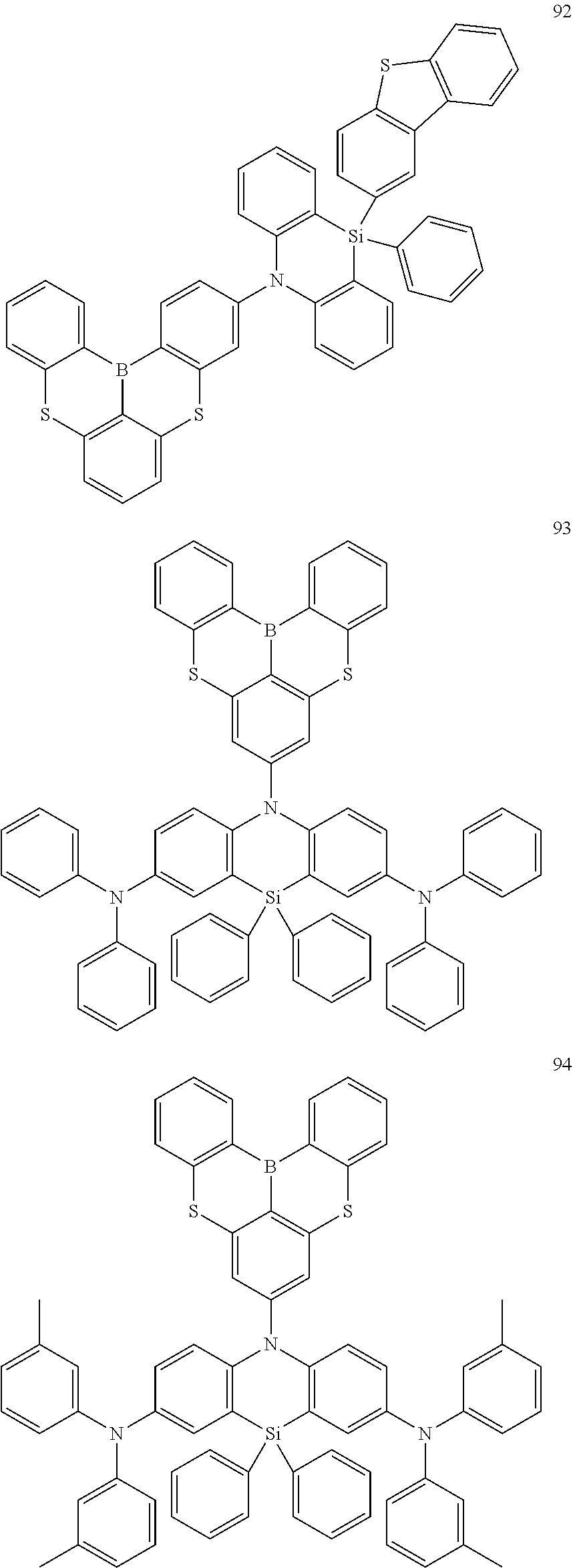
- the compound of an embodiment may be selected from one of the compounds represented by Compound Group 1, which includes Compounds 1 to 234.
- the electroluminescence device 10 of an embodiment may include at least one compound represented by Compound Group 1 in the emission layer EML.
- “ph” represents a phenyl group.
- At least one of the hydrogen atoms in the compound of an embodiment may be substituted with a deuterium atom.
- any hydrogen atom in a compound according to an embodiment may be substituted with a deuterium atom.
- the compound of an embodiment may have the same form as Compound 1-d corresponding to that in which a hydrogen atom is substituted with a deuterium atom in Compound 1 of Compound Group 1, and although not listed, the form in which any hydrogen atom is substituted with a deuterium atom may be equally provided for compounds in other embodiments described in Compound Group 1.
- the emission layer EML in the organic electroluminescence device 10 including the compound of an embodiment may emit a delayed fluorescence.
- the emission layer EML may emit a thermally activated delayed fluorescence (TADF).
- TADF thermally activated delayed fluorescence
- the organic electroluminescence device 10 of an embodiment may include multiple emission layers.
- the emission layers may be sequentially stacked and provided.
- the organic electroluminescence device 10 including the emission layers may emit white light.
- the organic electroluminescence device including emission layers may be an organic electroluminescence device having a tandem structure.
- at least one emission layer EML may include the above-described compound of an embodiment.
- the emission layer EML may include a host and a dopant, and may include the above-described compound of an embodiment as a dopant.
- the emission layer EML in the organic electroluminescence device 10 of an embodiment may include host for emitting a delayed fluorescence and a dopant for emitting a delayed fluorescence, and may include the above-described compound of an embodiment as a dopant for emitting a delayed fluorescence.
- the emission layer EML may include at least one of the compounds represented by Compound Group 1 as described above as a thermally activated delayed fluorescence dopant.
- the emission layer EML may be a delayed fluorescence emission layer, and the emission layer EML may include a known host material and the above-described compound.
- the compound of an embodiment may be used as a TADF dopant.
- the emission layer may include known host materials.
- the emission layer EML may include, as a host material, tris(8-hydroxyquinolino)aluminum (Alq 3 ), 4,4′-bis(N-carbazolyl)-1,1′-biphenyl (CBP), poly(N-vinylcabazole) (PVK), 9,10-di(naphthalene-2-yl)anthracene (ADN), 4,4′,4′′-tris(carbazol-9-yl)-triphenylamine (TCTA), 1,3,5-tris(1-phenyl-1H-benzo[d]imidazol-2-yl)benzene (TPBi), 3-tert-butyl-9,10-di(naphth-2-yl)anthracene (TBADN), distyrylarylene (DSA), 4,4′-bis(9-carbazolyl)-2,2′-di
- the emission layer EML in the organic electroluminescence device 10 of an embodiment may further include known dopant materials.
- the emission layer EML may further include, as dopant materials, styryl derivatives (e.g., 1,4-bis[2-(3-N-ethylcarbazolyl)vinyl]benzene (BCzVB), 4-(di-p-tolylamino)-4′-[(di-p-tolylamino)styryl]stilbene (DPAVB), and N-(4-((E)-2-(6-((E)-4-(diphenylamino)styryl)naphthalen-2-yl)vinyl)phenyl)-N-phenylbenzena mine (N-BDAVBi), perylene and the derivatives thereof (e.g., 2,5,8,11-tetra-t-butylperylene (TBP)), pyrene and the derivatives thereof (e.g., 1-dipyl
- the electron transport region ETR is provided on the emission layer EML.
- the electron transport region ETR may include at least one of a hole blocking layer HBL, an electron transport layer ETL, or an electron injection layer EIL, but an embodiment is not limited thereto.
- the electron transport region ETR may have a single layer formed of a single material, a single layer formed of different materials, or a multilayer structure including layers formed of different materials.
- the electron transport region ETR may have a single layer structure of an electron injection layer EIL or an electron transport layer ETL, and may have a single layer structure formed of an electron injection material and an electron transport material.
- the electron transport region ETR may have a single layer structure formed of different materials, or may have a structure in which an electron transport layer ETL/electron injection layer EIL and a hole blocking layer HBL/electron transport layer ETL/electron injection layer EIL are stacked in order from the emission layer EML, but is not limited thereto.
- the thickness of the electron transport region ETR may be, for example, in a range of about 1000 ⁇ to about 1,500 ⁇ .
- the electron transport region ETR may be formed using various methods such as a vacuum deposition method, a spin coating method, a cast method, a Langmuir-Blodgett (LB) method, an inkjet printing method, a laser printing method, a laser induced thermal imaging (LITI) method, etc.
- a vacuum deposition method such as a vacuum deposition method, a spin coating method, a cast method, a Langmuir-Blodgett (LB) method, an inkjet printing method, a laser printing method, a laser induced thermal imaging (LITI) method, etc.
- LB Langmuir-Blodgett
- LITI laser induced thermal imaging
- the electron transport region ETR may include an anthracene-based compound.
- the embodiments are not limited thereto, and the electron transport region may include, for example, tris(8-hydroxyquinolinato)aluminum (Alq 3 ), 1,3,5-tri[(3-pyridyl)-phen-3-yl]benzene, 2,4,6-tris(3′-(pyridin-3-yl)biphenyl-3-yl)-1,3,5-triazine, 2-(4-(N-phenylbenzoimidazol-1-yl)phenyl)-9,10-dinaphthylanthracene, 1,3,5-Tri(1-phenyl-1H-benzo[d]imidazol-2-yl)benzene (TPBi), 2,9-dimethyl-4,7-diphenyl-1,10-phenanthroline (BCP), 4,7-diphenyl-1,10-
- the thickness of the electron transport layers ETL may be in a range of about 100 ⁇ to about 1,000 ⁇ .
- the thickness of the electron transport layers ETL may be in a range of about 150 ⁇ to about 500 ⁇ . If the thickness of the electron transport layers ETL satisfies the above-described range, satisfactory electron transport characteristics may be obtained without a substantial increase in driving voltage.
- the electron transport region ETR may be formed using metal halides such as LiF, NaCl, CsF, RbCl, RbI, and CuI, lanthanum metals such as Yb, co-deposition of the metal halides and the lanthanum metals (e.g., KI:Yb or RbI:Yb, etc.), metal oxides such as Li 2 O and BaO, lithium quinolato (LiQ), etc., but the embodiments are not limited thereto.
- the electron injection layer EIL may also be formed of a mixture material of an electron transport material and an insulating organo-metal salt.
- the organo-metal salt may be a material having an energy band gap of greater than or equal to about 4 eV.
- the organo-metal salt may include metal acetates, metal benzoates, metal acetoacetates, metal acetylacetonates or metal stearates.
- the thickness of the electron injection layer EIL may be in a range of about 1 ⁇ to about 100 ⁇ .
- the thickness of the electron injection layer EIL may be in a range of about 3 ⁇ to about 90 ⁇ . If the thickness of the electron injection layers EIL satisfies the above-described range, satisfactory electron injection properties may be obtained without a substantial increase in driving voltage.
- the electron transport region ETR may include a hole blocking layer HBL as described above.
- the hole blocking layer HBL may include, for example, at least one of 2,9-dimethyl-4,7-diphenyl-1,10-phenanthroline (BCP), 4,7-diphenyl-1,10-phenanthroline (Bphen), DPEPO, and PPF, but is not limited thereto.
- the second electrode EL2 is provided on the electron transport region ETR.
- the second electrode EL2 may be a common electrode or cathode.
- the second electrode EL2 may be a transmissive electrode, a transflective electrode, or a reflective electrode.
- the second electrode EL2 may include a transparent metal oxide, for example, ITO, IZO, ZnO, ITZO, etc.
- the second electrode EL2 When the second electrode EL2 is a transflective electrode or a reflective electrode, the second electrode EL2 may include Ag, Mg, Cu, Al, Pt, Pd, Au, Ni, Nd, Ir, Cr, Li, Ca, LiF/Ca, LiF/Al, Mo, Ti, Yb, a compound thereof, or a mixture thereof (e.g., AgMg, AgYb, or MgAg). In other embodiments, the second electrode EL2 may have a multilayer structure including a reflective layer or a transflective layer formed of the above-described materials, and a transparent conductive layer formed of ITO, IZO, ZnO, ITZO, etc.
- the second electrode EL2 may be connected to an auxiliary electrode. If the second electrode EL2 is connected with the auxiliary electrode, the resistance of the second electrode EL2 may decrease.
- a capping layer CPL may be further disposed on the second electrode EL2 of the organic electroluminescence device 10 according to an embodiment.
- the refractive index of the capping layer CPL may be greater than or equal to about 1.6.
- the refractive index of the capping layer CPL may be greater than or equal to about 1.6 at a wavelength of about 589 nm.
- the capping layer CPL may be an organic layer or an inorganic layer.
- the inorganic material may include an alkaline metal compound such as LiF, an alkaline earth metal compound such as MgF 2 , SiON, SiN x , SiOy, etc.
- the organic material when the capping layer CPL includes an organic material, the organic material may include ⁇ -NPD, NPB, TPD, m-MTDATA, Alq 3 , CuPc, N4,N4,N4′,N4′-tetra(biphenyl-4-yl)biphenyl-4,4′-diamine (TPD15), 4,4′,4′′-tris(carbazol-9-yl)triphenylamine (TCTA), etc., or an epoxy resin, or acrylate such as methacrylate.
- the embodiments are not limited thereto, and the organic material may also include Compounds P1 to P5 below.
- a capping layer CPL may include an amine compound.
- the capping layer CPL may include at least one of Compound CPL1 or Compound CPL2 below.
- the organic electroluminescence device 10 may include the above-described compound of an embodiment in the emission layer EML disposed between the first electrode EL1 and the second electrode EL2 to exhibit excellent light emission efficiency.
- the organic electroluminescence device of an embodiment may exhibit high light emission efficiency in an emission wavelength region of blue light.
- the compound according to an embodiment may be a thermally activated delayed fluorescence dopant, and the emission layer EML may include the compound of an embodiment to emit a thermally activated delayed fluorescence, thereby exhibiting good light emission efficiency characteristics.
- the above-described compound of an embodiment may be included as a material for the organic electroluminescence device 10 in a functional layer in addition to the emission layer EML.
- the organic electroluminescence device 10 of an embodiment of the inventive concept may also include the above-described compound in at least one functional layer disposed between the first electrode EL1 and the second electrode EL2, or in the capping layer CPL disposed on the second electrode EL2.
- the organic electroluminescence device When the above-described compound of an embodiment is used as a material of the organic electroluminescence device by including an azasiline unit and a condensed cyclic unit containing an oxaborine or a thiaborine ring essentially containing a boron atom (B), efficiency of the organic electroluminescence device may be more improved. Furthermore, the organic electroluminescence device of an embodiment including the compound of an embodiment in the emission layer may emit deep blue light and exhibit high efficiency characteristics.
- a synthesis method for a compound according to an example will be described in detail by illustrating a synthetic method of Compounds 1, 55, and 60.
- a compound synthesis method is provided as an example, but the synthetic method for a compound according to an embodiment of the inventive concept is not limited to Examples below.
- Compound 1 according to an example may be synthesized by, for example, the steps shown in Reaction Scheme 1 below:
- Compound 55 according to an example may be synthesized by, for example, the steps shown in Reaction Formula 2 below:
- the crude product was purified by a silica gel column chromatography (using eluent having a 2:1 volume ratio of hexane and chloroform) to obtain Compound 55 which is a light yellow solid (0.14 g, yield 14%).
- Compound 55 was identified with NMR analysis.
- Compound 60 according to an example may be synthesized by, for example, the steps shown in Reaction Formula 3 below:
- the crude product was purified by a silica gel column chromatography (using eluent having a 2:1 volume ratio of hexane and chloroform) to obtain Compound 60 which is a light yellow solid (0.12 g, yield 11%).
- Compound 60 was identified with NMR analysis.
- Example Compounds have small ⁇ E ST values and thus may be used as a thermally activated delayed fluorescence dopant. It is believed that Example Compounds have smaller ⁇ E ST values compared to Comparative Example Compounds, and thus Example Compounds exhibit improved light emission emitting efficiency characteristics compared to Comparative Example Compounds.
- Example and Comparative Example Compounds the fluorescence quantum yield and fluorescence lifetime were evaluated.
- Samples for evaluation of fluorescence characteristics were prepared by depositing, on a quartz substrate, a composition including Example and Comparative Example Compounds for evaluation to form an organic film. Evaluation of the prepared samples were performed in an inert gas atmosphere. In the preparation of samples, DPEPO or PPF was used as a host material. In the prepared sample composition, an Example or Comparative Example Compound was contained to be 12 wt % to 50 wt % based on the total weight of the composition.
- the fluorescence emission characteristics were evaluated by measuring fluorescence emission spectra using a V-670 spectrometer from JASCO.
- the fluorescence quantum yield was determined by using a JASCO ILF-835 integrating sphere system using the same samples.
- Example Compounds emit deep blue light having the maximum emission wavelength of less than or equal to about 490 nm. It may be confirmed that Example Compounds exhibit fluorescence efficiency of 80% or greater to exhibit good light emission efficiency characteristics.
- the Example Compounds exhibit smaller delay time (Tau delay) compared to Comparative Example Compounds, and thus it may be predicted that delayed fluorescence efficiency of Example Compounds is more increased compared to Comparative Example Compounds.
- An evaluation of the organic electroluminescence device of an embodiment including the compound of an embodiment in the emission layer was carried out as follows. The method for manufacturing the organic electroluminescence device for the evaluation of the device is described below.
- Comparative Examples 1 and 2 are the organic electroluminescence devices manufactured by using each of Comparative Example Compounds C1 and C2 as a dopant material of the emission layer, respectively.
- the organic electroluminescence devices of Examples and Comparative Examples were manufactured as follows.
- An ITO was patterned on a glass substrate to form a first electrode.
- HAT-CN was deposited to a thickness of about 100 ⁇ to form a hole injection layer
- TAPC was deposited to a thickness of about 500 ⁇ to form a hole transport layer
- a 100 ⁇ -thick electron blocking layer EBL was formed with mDCP.
- an Example Compound and PPF were co-deposited in a ratio of about 20:80 to form a 200 ⁇ -thick layer.
- the emission layer formed by co-depositing was deposited by mixing an Example Compound and PPF.
- a 100 ⁇ -thick layer was formed on the emission layer by using PPF, a 300 ⁇ -thick layer was formed with B3PyPB, and a 10 ⁇ -thick layer was formed with LiF to form an electron transport region.
- a second electrode having a thickness of about 1,000 ⁇ was formed with aluminum (Al).
- the evaluation results of the organic electroluminescence devices of Examples and Comparative Examples are listed in Table 4.
- a maximum emission wavelength ( ⁇ max ) and an external quantum efficiency ( ⁇ ext) of the manufactured organic electroluminescence devices are listed in Table 4 for comparison.
- the maximum emission wavelength ( ⁇ max ) represents the wavelength showing the maximum value in the emission spectrum.
- the organic electroluminescence devices of Examples emit light in a blue wavelength region of less than or equal to about 480 nm to exhibit high light emission efficiency characteristics. It may be confirmed that Examples 1 to 3 exhibit higher external quantum efficiency values compared to Comparative Examples.
- the compound of an example may include at least one condensed cyclic unit containing a boron atom and at least one azasiline unit bonded to the condensed cyclic unit to facilitate the reverse intersystem crossing, thereby exhibiting excellent light emission efficiency.
- the organic electroluminescence device of an example may include the compound of an example in the emission layer to exhibit high light emission efficiency in a deep blue emission wavelength region.
- the organic electroluminescence device of an embodiment may exhibit excellent light emission efficiency.
- the compound of an embodiment may be contained in the emission layer of the organic electroluminescence device to contribute to high efficiency of the organic electroluminescence device.
Landscapes
- Chemical & Material Sciences (AREA)
- Engineering & Computer Science (AREA)
- Materials Engineering (AREA)
- Physics & Mathematics (AREA)
- Spectroscopy & Molecular Physics (AREA)
- Organic Chemistry (AREA)
- Optics & Photonics (AREA)
- Electroluminescent Light Sources (AREA)
- Inorganic Chemistry (AREA)
Abstract

Description


| TABLE 1 | |
| Compound 1 |
 |
| Compound 55 |
 |
| Compound 60 |
 |
| Compound 65 |
 |
| Comparative Example Compound C1 |
 |
| Comparative Example Compound C2 |
 |
| Comparative Example Compound C3 |
 |
| Comparative Example Compound C4 |
 |
| Comparative Example Compound C5 |
 |
| TABLE 2 | |||||
| Compound | S1 (eV) | T1 (eV) | ΔEST (eV) | ||
| 1 | 2.7410 | 2.7351 | 0.0059 | ||
| 55 | 2.6618 | 2.6575 | 0.0043 | ||
| 60 | 2.5296 | 2.5228 | 0.0068 | ||
| 65 | 2.7078 | 2.7022 | 0.0056 | ||
| C1 | 2.7662 | 2.7572 | 0.0090 | ||
| C2 | 2.6278 | 2.6198 | 0.0080 | ||
| C3 | 2.2335 | 2.2265 | 0.0070 | ||
| C4 | 3.0613 | 2.6170 | 0.4443 | ||
| C5 | 2.9278 | 2.9196 | 0.0082 | ||
| TABLE 3 | |||||
| Compound | PLλmax (nm) | PLQY (%) | Tau delay/μsec | ||
| 1 | 451 | 81 | 1.9 | ||
| 55 | 465 | 98 | 2.3 | ||
| 60 | 484 | 99 | 1.6 | ||
| C1 | 439 | 68 | 6.0 | ||
| C2 | 453 | 75 | 4.5 | ||
| C3 | 492 | 92 | 2.6 | ||

(Evaluation of Organic Electroluminescence Device Characteristics)
| TABLE 4 | |||
| Device manufactured | |||
| examples | Dopant Material | λmax (nm) | ηext (%) |
| Example 1 | Example Compound 1 | 457 | 21.2 |
| Example 2 | Example Compound 55 | 464 | 31.7 |
| Example 3 | Example Compound 60 | 478 | 32.0 |
| Comparative | Comparative Example | 445 | 15.7 |
| Example 1 | Compound C1 | ||
| Comparative | Comparative Example | 459 | 20.6 |
| Example 2 | Compound C2 | ||
Claims (19)


Applications Claiming Priority (2)
| Application Number | Priority Date | Filing Date | Title |
|---|---|---|---|
| KR10-2020-0052327 | 2020-04-29 | ||
| KR1020200052327A KR102827472B1 (en) | 2020-04-29 | 2020-04-29 | Organic electroluminescence device and compound for organic electroluminescence device |
Publications (2)
| Publication Number | Publication Date |
|---|---|
| US20210351361A1 US20210351361A1 (en) | 2021-11-11 |
| US12178123B2 true US12178123B2 (en) | 2024-12-24 |
Family
ID=75728746
Family Applications (1)
| Application Number | Title | Priority Date | Filing Date |
|---|---|---|---|
| US17/179,837 Active 2042-08-26 US12178123B2 (en) | 2020-04-29 | 2021-02-19 | Organic electroluminescence device and compound for organic electroluminescence device |
Country Status (5)
| Country | Link |
|---|---|
| US (1) | US12178123B2 (en) |
| EP (1) | EP3905361B1 (en) |
| JP (1) | JP7805713B2 (en) |
| KR (1) | KR102827472B1 (en) |
| CN (1) | CN113563373A (en) |
Citations (12)
| Publication number | Priority date | Publication date | Assignee | Title |
|---|---|---|---|---|
| US20060113907A1 (en) * | 2004-11-26 | 2006-06-01 | Ja-Hyun Im | Organic light emitting display and method for fabricating the same |
| US20150236274A1 (en) * | 2014-02-18 | 2015-08-20 | Kwansei Gakuin Educational Foundation | Polycyclic aromatic compound |
| WO2017018326A1 (en) | 2015-07-24 | 2017-02-02 | コニカミノルタ株式会社 | Organic electroluminescent element, display device, and illumination device |
| US20180019415A1 (en) | 2016-07-13 | 2018-01-18 | Samsung Display Co., Ltd. | Polycyclic compound and organic electroluminescence device including the same |
| KR101876763B1 (en) | 2017-05-22 | 2018-07-11 | 머티어리얼사이언스 주식회사 | Organic compound and organic electroluminescent device comprising the same |
| KR101886773B1 (en) | 2014-02-18 | 2018-08-08 | 가꼬우 호징 관세이 가쿠잉 | Polycyclic aromatic compound |
| CN108774258A (en) | 2018-09-10 | 2018-11-09 | 西安瑞联新材料股份有限公司 | A kind of Heterocyclic Compound Containing Boron and its application in organic electro-optic device |
| US20190312210A1 (en) | 2018-04-05 | 2019-10-10 | Samsung Display Co., Ltd. | Organic electroluminescence device and polycyclic compound for organic electroluminescence device |
| US20200028084A1 (en) * | 2018-07-19 | 2020-01-23 | Lg Display Co., Ltd. | Organic electroluminescent device |
| US20200403158A1 (en) | 2019-06-21 | 2020-12-24 | Samsung Display Co., Ltd. | Organic electroluminescence device and compound for organic electroluminescence device |
| US20210053998A1 (en) * | 2018-07-24 | 2021-02-25 | Material Science Co., Ltd. | Organic electroluminescent element |
| KR20210088445A (en) | 2020-01-06 | 2021-07-14 | 경상국립대학교산학협력단 | Novel compound and organic light-emitting diode using them |
Family Cites Families (3)
| Publication number | Priority date | Publication date | Assignee | Title |
|---|---|---|---|---|
| CA3073055A1 (en) | 2017-09-04 | 2019-03-07 | Agenus Inc. | T cell receptors that bind to mixed lineage leukemia (mll)-specific phosphopeptides and methods of use thereof |
| KR102260883B1 (en) * | 2018-07-19 | 2021-06-07 | 엘지디스플레이 주식회사 | Organic electroluminescent device |
| JP7595304B2 (en) * | 2019-04-26 | 2024-12-06 | 学校法人関西学院 | Compound, material for organic device, composition for forming light-emitting layer, organic field-effect transistor, organic thin-film solar cell, organic electroluminescent device, display device, and lighting device |
-
2020
- 2020-04-29 KR KR1020200052327A patent/KR102827472B1/en active Active
-
2021
- 2021-02-19 US US17/179,837 patent/US12178123B2/en active Active
- 2021-04-19 JP JP2021070640A patent/JP7805713B2/en active Active
- 2021-04-19 CN CN202110418986.4A patent/CN113563373A/en active Pending
- 2021-04-28 EP EP21171002.5A patent/EP3905361B1/en active Active
Patent Citations (20)
| Publication number | Priority date | Publication date | Assignee | Title |
|---|---|---|---|---|
| US20060113907A1 (en) * | 2004-11-26 | 2006-06-01 | Ja-Hyun Im | Organic light emitting display and method for fabricating the same |
| US20150236274A1 (en) * | 2014-02-18 | 2015-08-20 | Kwansei Gakuin Educational Foundation | Polycyclic aromatic compound |
| KR101886773B1 (en) | 2014-02-18 | 2018-08-08 | 가꼬우 호징 관세이 가쿠잉 | Polycyclic aromatic compound |
| US10374166B2 (en) | 2014-02-18 | 2019-08-06 | Kwansei Gakuin Educational Foundation | Polycyclic aromatic compound |
| WO2017018326A1 (en) | 2015-07-24 | 2017-02-02 | コニカミノルタ株式会社 | Organic electroluminescent element, display device, and illumination device |
| US10651395B2 (en) | 2015-07-24 | 2020-05-12 | Konica Minolta, Inc. | Organic electroluminescent element, display device, and illumination device |
| US10333085B2 (en) | 2016-07-13 | 2019-06-25 | Samsung Display Co., Ltd. | Polycyclic compound and organic electroluminescence device including the same |
| US20180019415A1 (en) | 2016-07-13 | 2018-01-18 | Samsung Display Co., Ltd. | Polycyclic compound and organic electroluminescence device including the same |
| KR20180007727A (en) | 2016-07-13 | 2018-01-24 | 삼성디스플레이 주식회사 | Polycyclic compound and organic electroluminescence device including the same |
| KR101876763B1 (en) | 2017-05-22 | 2018-07-11 | 머티어리얼사이언스 주식회사 | Organic compound and organic electroluminescent device comprising the same |
| KR101976556B1 (en) | 2017-05-22 | 2019-05-09 | 머티어리얼사이언스 주식회사 | Organic compound and organic electroluminescent device comprising the same |
| US20200176679A1 (en) | 2017-05-22 | 2020-06-04 | Material Science Co., Ltd. | Organic compound and organic electroluminescent device comprising the same |
| US20190312210A1 (en) | 2018-04-05 | 2019-10-10 | Samsung Display Co., Ltd. | Organic electroluminescence device and polycyclic compound for organic electroluminescence device |
| KR20190117038A (en) | 2018-04-05 | 2019-10-16 | 삼성디스플레이 주식회사 | Organic electroluminescence device and polycyclic compound for organic electroluminescence device |
| US20200028084A1 (en) * | 2018-07-19 | 2020-01-23 | Lg Display Co., Ltd. | Organic electroluminescent device |
| US20210053998A1 (en) * | 2018-07-24 | 2021-02-25 | Material Science Co., Ltd. | Organic electroluminescent element |
| CN108774258A (en) | 2018-09-10 | 2018-11-09 | 西安瑞联新材料股份有限公司 | A kind of Heterocyclic Compound Containing Boron and its application in organic electro-optic device |
| US20200403158A1 (en) | 2019-06-21 | 2020-12-24 | Samsung Display Co., Ltd. | Organic electroluminescence device and compound for organic electroluminescence device |
| KR20200145945A (en) | 2019-06-21 | 2020-12-31 | 삼성디스플레이 주식회사 | Organic electroluminescence device and compound for organic electroluminescence device |
| KR20210088445A (en) | 2020-01-06 | 2021-07-14 | 경상국립대학교산학협력단 | Novel compound and organic light-emitting diode using them |
Non-Patent Citations (4)
| Title |
|---|
| Dongdong Song et al., "Asymmetric thermally activated delayed fluorescence (TADF) emitters with 5,9-dioxa-13b-boranaphtho[3,2,1-de]anthracene (OBA) as the acceptor and highly efficient blue-emitting OLEDs", Journal of Materials Chemistry C, Sep. 3, 2019, pp. 11953-11963, vol. 7. |
| Guoyun Meng et al., "Isomeric Bright Sky-Blue TADF Emitters Based on Bisacridine Decorated DBNA: Impact of Donor Locations on Luminescent and Electroluminescent Properties", Advanced Optical Materials, Mar. 25, 2019, pp. 1-14, vol. 7, No. 1900130. |
| Hiroki Hirai et al., "One-Step Borylation of 1,3-Diaryloxybenzenes Towards Efficient Materials for Organic Light-Emitting Diodes", Angewandte Chemie International Edition, Sep. 18, 2015, pp. 13581-13585, vol. 54. |
| UCAR—Center for Science Education, "Wavelength of Blue and Red Ligh", pp. 1-2. * |
Also Published As
| Publication number | Publication date |
|---|---|
| KR20210134116A (en) | 2021-11-09 |
| JP2021174990A (en) | 2021-11-01 |
| JP7805713B2 (en) | 2026-01-26 |
| EP3905361B1 (en) | 2022-12-21 |
| CN113563373A (en) | 2021-10-29 |
| KR102827472B1 (en) | 2025-07-02 |
| EP3905361A1 (en) | 2021-11-03 |
| US20210351361A1 (en) | 2021-11-11 |
Similar Documents
| Publication | Publication Date | Title |
|---|---|---|
| US11489124B2 (en) | Organic electroluminescence device and fused polycyclic compound for organic electroluminescence device | |
| US20200185626A1 (en) | Organic electroluminescence device and polycyclic compound for organic electroluminescence device | |
| US20190296247A1 (en) | Organic electroluminescence device and polycyclic compound for organic electroluminescence device | |
| US11839150B2 (en) | Organic electroluminescence device and condensed cyclic compound for organic electroluminescence device | |
| US12035617B2 (en) | Organic electroluminescence device and organometallic compound for organic electroluminescence device | |
| US11581493B2 (en) | Organic electroluminescence device and condensed polycyclic compound for organic electroluminescence device | |
| US11393985B2 (en) | Organic electroluminescence device and polycyclic compound for organic electroluminescence device | |
| US11889752B2 (en) | Organic electroluminescence device and polycyclic compound for organic electroluminescence device | |
| US20180205019A1 (en) | Organic electroluminescence device | |
| US11276836B2 (en) | Organic electroluminescence device and polycyclic compound for organic electroluminescence device | |
| US11515486B2 (en) | Organic electroluminescence device and polycyclic compound for organic electroluminescence device | |
| US11502259B2 (en) | Organic electroluminescence device and polycyclic compound for organic electroluminescence device | |
| US12256633B2 (en) | Organic electroluminescence device and fused polycyclic compound for organic electroluminescence device | |
| US20200243769A1 (en) | Organic electroluminescence device and polycyclic compound for organic electroluminescence device | |
| US12108667B2 (en) | Organic electroluminescence device and spiro compound for organic electroluminescence device | |
| US20210399227A1 (en) | Organic electroluminescence device and fused polycyclic compound for organic electroluminescence device | |
| US11832506B2 (en) | Organic electroluminescence device and fused polycyclic compound for organic electroluminescence device | |
| US11800786B2 (en) | Organic electroluminescence device and polycyclic compound for organic electroluminescence device | |
| US12439820B2 (en) | Organic electroluminescence device and amine compound for organic electroluminescence device | |
| US11985893B2 (en) | Organic electroluminescence device and aromatic compound for organic electroluminescence device | |
| US11569457B2 (en) | Organic electroluminescence device and polycyclic compound for organic electroluminescence device | |
| US11335862B2 (en) | Organic electroluminescence device and polycyclic compound for organic electroluminescence device | |
| US20220123227A1 (en) | Organic electroluminescence device and fused polycyclic compound for organic electroluminescence device | |
| US11805695B2 (en) | Organic electroluminescence device and polycyclic compound for organic electroluminescence device | |
| US12178123B2 (en) | Organic electroluminescence device and compound for organic electroluminescence device |
Legal Events
| Date | Code | Title | Description |
|---|---|---|---|
| AS | Assignment |
Owner name: KYUSHU UNIVERSITY, NATIONAL UNIVERSITY CORPORATION, JAPAN Free format text: ASSIGNMENT OF ASSIGNORS INTEREST;ASSIGNORS:MIYAZAKI, YUUKI;SUZAKI, YUJI;PARK, IN SEOB;AND OTHERS;SIGNING DATES FROM 20201023 TO 20201110;REEL/FRAME:055338/0386 Owner name: SAMSUNG DISPLAY CO., LTD., KOREA, REPUBLIC OF Free format text: ASSIGNMENT OF ASSIGNORS INTEREST;ASSIGNORS:MIYAZAKI, YUUKI;SUZAKI, YUJI;PARK, IN SEOB;AND OTHERS;SIGNING DATES FROM 20201023 TO 20201110;REEL/FRAME:055338/0386 |
|
| FEPP | Fee payment procedure |
Free format text: ENTITY STATUS SET TO UNDISCOUNTED (ORIGINAL EVENT CODE: BIG.); ENTITY STATUS OF PATENT OWNER: LARGE ENTITY |
|
| STPP | Information on status: patent application and granting procedure in general |
Free format text: DOCKETED NEW CASE - READY FOR EXAMINATION |
|
| STPP | Information on status: patent application and granting procedure in general |
Free format text: NON FINAL ACTION MAILED |
|
| STPP | Information on status: patent application and granting procedure in general |
Free format text: RESPONSE TO NON-FINAL OFFICE ACTION ENTERED AND FORWARDED TO EXAMINER |
|
| STPP | Information on status: patent application and granting procedure in general |
Free format text: FINAL REJECTION MAILED |
|
| STPP | Information on status: patent application and granting procedure in general |
Free format text: ADVISORY ACTION MAILED |
|
| STPP | Information on status: patent application and granting procedure in general |
Free format text: DOCKETED NEW CASE - READY FOR EXAMINATION |
|
| STPP | Information on status: patent application and granting procedure in general |
Free format text: NON FINAL ACTION MAILED |
|
| STPP | Information on status: patent application and granting procedure in general |
Free format text: RESPONSE TO NON-FINAL OFFICE ACTION ENTERED AND FORWARDED TO EXAMINER |
|
| STPP | Information on status: patent application and granting procedure in general |
Free format text: NOTICE OF ALLOWANCE MAILED -- APPLICATION RECEIVED IN OFFICE OF PUBLICATIONS |
|
| ZAAB | Notice of allowance mailed |
Free format text: ORIGINAL CODE: MN/=. |
|
| STPP | Information on status: patent application and granting procedure in general |
Free format text: AWAITING TC RESP., ISSUE FEE NOT PAID |
|
| STPP | Information on status: patent application and granting procedure in general |
Free format text: NOTICE OF ALLOWANCE MAILED -- APPLICATION RECEIVED IN OFFICE OF PUBLICATIONS |
|
| STPP | Information on status: patent application and granting procedure in general |
Free format text: PUBLICATIONS -- ISSUE FEE PAYMENT RECEIVED |
|
| STPP | Information on status: patent application and granting procedure in general |
Free format text: PUBLICATIONS -- ISSUE FEE PAYMENT VERIFIED |
|
| STPP | Information on status: patent application and granting procedure in general |
Free format text: PUBLICATIONS -- ISSUE FEE PAYMENT VERIFIED |
|
| STCF | Information on status: patent grant |
Free format text: PATENTED CASE |