US12127361B2 - Modular memory devices - Google Patents
Modular memory devices Download PDFInfo
- Publication number
- US12127361B2 US12127361B2 US17/577,393 US202217577393A US12127361B2 US 12127361 B2 US12127361 B2 US 12127361B2 US 202217577393 A US202217577393 A US 202217577393A US 12127361 B2 US12127361 B2 US 12127361B2
- Authority
- US
- United States
- Prior art keywords
- plate
- memory
- connector
- memory module
- module
- Prior art date
- Legal status (The legal status is an assumption and is not a legal conclusion. Google has not performed a legal analysis and makes no representation as to the accuracy of the status listed.)
- Active, expires
Links
Images


Classifications
-
- G—PHYSICS
- G06—COMPUTING OR CALCULATING; COUNTING
- G06F—ELECTRIC DIGITAL DATA PROCESSING
- G06F3/00—Input arrangements for transferring data to be processed into a form capable of being handled by the computer; Output arrangements for transferring data from processing unit to output unit, e.g. interface arrangements
- G06F3/06—Digital input from, or digital output to, record carriers, e.g. RAID, emulated record carriers or networked record carriers
- G06F3/0601—Interfaces specially adapted for storage systems
- G06F3/0628—Interfaces specially adapted for storage systems making use of a particular technique
- G06F3/0638—Organizing or formatting or addressing of data
- G06F3/064—Management of blocks
-
- H—ELECTRICITY
- H05—ELECTRIC TECHNIQUES NOT OTHERWISE PROVIDED FOR
- H05K—PRINTED CIRCUITS; CASINGS OR CONSTRUCTIONAL DETAILS OF ELECTRIC APPARATUS; MANUFACTURE OF ASSEMBLAGES OF ELECTRICAL COMPONENTS
- H05K5/00—Casings, cabinets or drawers for electric apparatus
- H05K5/02—Details
- H05K5/0256—Details of interchangeable modules or receptacles therefor, e.g. cartridge mechanisms
- H05K5/026—Details of interchangeable modules or receptacles therefor, e.g. cartridge mechanisms having standardized interfaces
-
- G—PHYSICS
- G06—COMPUTING OR CALCULATING; COUNTING
- G06F—ELECTRIC DIGITAL DATA PROCESSING
- G06F3/00—Input arrangements for transferring data to be processed into a form capable of being handled by the computer; Output arrangements for transferring data from processing unit to output unit, e.g. interface arrangements
- G06F3/06—Digital input from, or digital output to, record carriers, e.g. RAID, emulated record carriers or networked record carriers
- G06F3/0601—Interfaces specially adapted for storage systems
- G06F3/0602—Interfaces specially adapted for storage systems specifically adapted to achieve a particular effect
- G06F3/0604—Improving or facilitating administration, e.g. storage management
- G06F3/0607—Improving or facilitating administration, e.g. storage management by facilitating the process of upgrading existing storage systems, e.g. for improving compatibility between host and storage device
-
- G—PHYSICS
- G06—COMPUTING OR CALCULATING; COUNTING
- G06F—ELECTRIC DIGITAL DATA PROCESSING
- G06F3/00—Input arrangements for transferring data to be processed into a form capable of being handled by the computer; Output arrangements for transferring data from processing unit to output unit, e.g. interface arrangements
- G06F3/06—Digital input from, or digital output to, record carriers, e.g. RAID, emulated record carriers or networked record carriers
- G06F3/0601—Interfaces specially adapted for storage systems
- G06F3/0628—Interfaces specially adapted for storage systems making use of a particular technique
- G06F3/0655—Vertical data movement, i.e. input-output transfer; data movement between one or more hosts and one or more storage devices
- G06F3/0658—Controller construction arrangements
-
- G—PHYSICS
- G06—COMPUTING OR CALCULATING; COUNTING
- G06F—ELECTRIC DIGITAL DATA PROCESSING
- G06F3/00—Input arrangements for transferring data to be processed into a form capable of being handled by the computer; Output arrangements for transferring data from processing unit to output unit, e.g. interface arrangements
- G06F3/06—Digital input from, or digital output to, record carriers, e.g. RAID, emulated record carriers or networked record carriers
- G06F3/0601—Interfaces specially adapted for storage systems
- G06F3/0668—Interfaces specially adapted for storage systems adopting a particular infrastructure
- G06F3/0671—In-line storage system
- G06F3/0673—Single storage device
- G06F3/0679—Non-volatile semiconductor memory device, e.g. flash memory, one time programmable memory [OTP]
-
- G—PHYSICS
- G06—COMPUTING OR CALCULATING; COUNTING
- G06F—ELECTRIC DIGITAL DATA PROCESSING
- G06F3/00—Input arrangements for transferring data to be processed into a form capable of being handled by the computer; Output arrangements for transferring data from processing unit to output unit, e.g. interface arrangements
- G06F3/06—Digital input from, or digital output to, record carriers, e.g. RAID, emulated record carriers or networked record carriers
- G06F3/0601—Interfaces specially adapted for storage systems
- G06F3/0668—Interfaces specially adapted for storage systems adopting a particular infrastructure
- G06F3/0671—In-line storage system
- G06F3/0683—Plurality of storage devices
- G06F3/0688—Non-volatile semiconductor memory arrays
-
- G—PHYSICS
- G11—INFORMATION STORAGE
- G11C—STATIC STORES
- G11C5/00—Details of stores covered by group G11C11/00
- G11C5/02—Disposition of storage elements, e.g. in the form of a matrix array
- G11C5/04—Supports for storage elements, e.g. memory modules; Mounting or fixing of storage elements on such supports
-
- H—ELECTRICITY
- H05—ELECTRIC TECHNIQUES NOT OTHERWISE PROVIDED FOR
- H05K—PRINTED CIRCUITS; CASINGS OR CONSTRUCTIONAL DETAILS OF ELECTRIC APPARATUS; MANUFACTURE OF ASSEMBLAGES OF ELECTRICAL COMPONENTS
- H05K5/00—Casings, cabinets or drawers for electric apparatus
- H05K5/0026—Casings, cabinets or drawers for electric apparatus provided with connectors and printed circuit boards [PCB], e.g. automotive electronic control units
-
- H—ELECTRICITY
- H05—ELECTRIC TECHNIQUES NOT OTHERWISE PROVIDED FOR
- H05K—PRINTED CIRCUITS; CASINGS OR CONSTRUCTIONAL DETAILS OF ELECTRIC APPARATUS; MANUFACTURE OF ASSEMBLAGES OF ELECTRICAL COMPONENTS
- H05K7/00—Constructional details common to different types of electric apparatus
- H05K7/14—Mounting supporting structure in casing or on frame or rack
- H05K7/1422—Printed circuit boards receptacles, e.g. stacked structures, electronic circuit modules or box like frames
- H05K7/1427—Housings
-
- H—ELECTRICITY
- H05—ELECTRIC TECHNIQUES NOT OTHERWISE PROVIDED FOR
- H05K—PRINTED CIRCUITS; CASINGS OR CONSTRUCTIONAL DETAILS OF ELECTRIC APPARATUS; MANUFACTURE OF ASSEMBLAGES OF ELECTRICAL COMPONENTS
- H05K7/00—Constructional details common to different types of electric apparatus
- H05K7/20—Modifications to facilitate cooling, ventilating, or heating
- H05K7/2039—Modifications to facilitate cooling, ventilating, or heating characterised by the heat transfer by conduction from the heat generating element to a dissipating body
- H05K7/20436—Inner thermal coupling elements in heat dissipating housings, e.g. protrusions or depressions integrally formed in the housing
- H05K7/20445—Inner thermal coupling elements in heat dissipating housings, e.g. protrusions or depressions integrally formed in the housing the coupling element being an additional piece, e.g. thermal standoff
Definitions
- the application generally relates to memory technology, and particularly to modular memory devices with replaceable memory module(s).
- SSDs Solid-state drives
- EDSFF Enterprise and Data Center Standard Form Factor
- SFF-TA-1002 A card edge connector as defined in SFF-TA-1002 can be used to electrically connect the E3 device to a host system such as a server.
- An objective of the present application is to provide a memory device with a modular design.
- a memory device in an aspect of the present application, there is provided a memory device.
- the memory device includes a connector plate having a front edge and a rear edge opposite to the front edge, wherein the connector plate comprises an edge connector disposed at the rear edge and configured to connect to a host connector of a host device; a controller plate defining a first connection region, a second connection region and a chip region, wherein the controller plate is attached to the connector plate at the first connection region, and the controller plate comprises a memory control module disposed in the chip region and in electrical communication with the edge connector; and at least one memory module detachably connected to the controller plate at the second connection region of the controller plate, wherein each of the at least one memory module is in electrical communication with the memory control module when the memory module is connected to the controller plate, such that the memory module can be accessible by the host device via the memory control module.
- the chip region is between the first connection region and the second connection region.
- the second connection region does not overlay with the connector plate.
- the controller plate comprises a bottom side facing the connector plate and a top side opposite to the bottom side, and the memory control module is disposed on the top side of the controller plate.
- the at least one memory module comprises a first memory module connected to the top side of the controller plate and a second memory module connected to the bottom side of the controller plate.
- the second memory module is at the same layer as the connector plate.
- the memory device further comprising a heat conductive layer disposed between the first memory module and the second memory module.
- the at least one memory module comprises a memory module connected to the top side of the controller plate at the second connection region of the controller plate.
- the memory device further comprising a heatsink disposed on the memory control module.
- the memory device further comprising a chassis for enclosing the connector plate, the controller plate and the at least one memory module.
- the chassis comprises an opening close to the rear edge of the connector plate and through which the edge connector protrudes out of the chassis.
- the memory device further comprising: a first set of retention pins passing through the connector plate and the controller plate at the first connection region of the controller plate, wherein the first set of retention pins are configured to secure the connector plate and the controller plate to the chassis.
- the memory device further comprising: a second set of retention pins passing through at least one of the connector plate and the controller plate and disposed close to the front edge of the controller plate, wherein the second set of retention pins are configured to secure the connector plate with the controller plate.
- the memory device further comprising: a third set of retention pins passing through the controller plate and the at least one memory module at the second connection region of the controller plate, wherein the third set of retention pins are configured to secure the controller plate and the at least one memory module to the chassis.
- the memory device further comprising: a fourth set of retention pins passing through the at least one memory module, wherein the fourth set of retention pins are configured to secure the at least one memory module to the chassis.
- the memory device further comprising a heat conductive layer disposed between one of the at least one memory module and the chassis.
- each of the at least one memory module is a single-sided memory module or a double-sided memory module.
- the edge connector is compatible with the SFF-TA-1002 standard.
- the memory device further comprising: a first flexible cable configured to electrically connect the edge connector with the memory control module; and at least one second flexible cable configured to electrically connect the memory control module with the at least one memory module, respectively.
- the memory device includes a connector plate having a front edge and a rear edge opposite to the front edge, wherein the connector plate includes: an edge connector disposed at the rear edge and configured to connect to a host connector of a host device; and a memory control module disposed on the connector plate and in electrical communication with the edge connector; a bridge plate defining a first connection region and a second connection region, wherein the bridge plate is attached to the connector plate at the first connection region; and at least one memory module detachably connected to the bridge plate at the second connection region of the bridge plate, wherein each of the at least one memory module is in electrical communication with the memory control module when the memory module is connected to the bridge plate, such that the memory module can be accessible by the host device via the memory control module.
- a memory device in another aspect of the present application, there is provided a memory device.
- the memory device includes a connector plate having a front edge and a rear edge opposite to the front edge, and defining a connection region and a chip region between the rear edge and the front edge, wherein the connector plate comprises: an edge connector disposed at the rear edge and configured to connect to a host connector of a host device; a memory control module disposed in the chip region and in electrical communication with the edge connector; and a memory module detachably connected to the connector plate at the connection region of the connector plate, wherein the memory module is in electrical communication with the memory control module when the memory module is connected to the connector plate, such that the memory module can be accessible by the host device via the memory control module.
- connection region does not overlay with the connector plate.
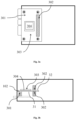
- FIG. 1 a shows an exemplary memory device 10 with a modular design according to an embodiment of the present application
- FIG. 1 b shows a front view thereof.
- FIG. 2 a shows an exemplary connector plate 101 of the memory device 10 shown in FIGS. 1 a and 1 b
- FIG. 2 b shows a front view thereof.
- FIG. 3 a shows an exemplary controller plate 102 of the memory device 10 shown in FIGS. 1 a and 1 b
- FIG. 3 b shows a front view thereof.
- FIG. 4 a shows an exemplary memory device 40 with a modular design according to an embodiment of the present application
- FIG. 4 b shows a front view thereof.
- FIGS. 5 a to 5 d show exemplary memory modules that may be connected to the memory devices according to embodiments of the present application.
- FIG. 6 shows an exemplary connection between a controller plate and a memory module of a memory device according to an embodiment of the present application.
- FIG. 7 shows an exemplary memory device 100 with a modular design according to an embodiment of the present application.
- layer means a spatial level within which the components can be arranged. When some of the components are arranged in one layer, it means that these components are generally at the same height with reference to a base plane, for example, a plate.
- the plate described herein may be implemented as a circuit board, for example, a printed circuit board (PCB).
- PCB printed circuit board
- FIGS. 1 a to 4 b described with the following embodiments are drawn in a planar view in collaboration with a front view thereof. These figures are not drawn in scale, and some parts are exaggerated to illustrate the principles of the present application more clearly.
- FIGS. 1 a and 1 b show a memory device 10 with a modular design according to an embodiment of the present application.
- FIGS. 2 a , 1 b , 3 a and 3 b show a connector plate and a controller plate of the memory device 10 shown in FIGS. 1 a and 1 b.
- the memory device 10 includes a connector plate 101 , which has a front edge 201 and a rear edge 202 opposite to each other.
- the front edge 201 can be disposed within a chassis 104 that encloses the connector plate 101 and various other components of the memory device 10 , while the rear edge 202 can be displaced out of the chassis 104 .
- the connector plate 101 further includes an edge connector 203 , which is disposed at the rear edge 202 .
- the edge connector 203 can connect to a host connector of a host device (not shown for simplicity) to enable electrical communication therebetween.
- the edge connector 203 can be built in various other forms, for example, depending on what standard the host connector is compatible with.
- the edge connector 203 can be in form of single-sided or double-sided “golden fingers” (i.e. contacts) that is known in the industry.
- the edge connector 203 can be compatible with the SFF-TA-1002 standard.
- the SFF-TA-1002 standard defines an unshielded, input/output, card edge connector and mating card interface which is configurable for straight, right angle, straddle mount, and orthogonal applications.
- the SFF-TA-1002 standard and some other relevant SFF standards including the SFF-TA-1006, SFF-TA-1008, SFF-TA-1009 standards can be found at the SNIA official website (www.snia.org/technology-communities/sff/specifications), the entire contents of which are incorporated herein by reference.
- the memory devices according to the embodiments of the present application can be directly connected to existing devices, for example, the host devices that have SFF-TA-1002 connectors or ports.
- the host device described herein may be a computer or a smart device that may need additional memory devices for data storage purposes.
- the memory device 10 further includes a controller plate 102 , which is electrically connected to the connector plate 101 .
- the controller plate 102 defines a first connection region 301 , a second connection region 302 , and a chip region 303 between the first and second connection regions.
- the connection regions described herein may extend across the entire control plate 102 from one side to another.
- the controller plate 102 includes a memory control module 304 that handles control tasks for the memory device 10 .
- the memory control module (chip) 304 is disposed in the chip region 303 and is in electrical communication with the edge connector 203 as shown in FIG.
- the memory control module 304 resides in the chip region 303 and handles control tasks of the memory device 10 , the chip region 303 can be deemed as a “hub” of the memory device 10 in the dimension of information and data. It can be appreciated that although a single memory control module 304 is shown in FIGS. 3 a and 3 b , some other circuit components can be disposed in the controller plate 102 , including other circuit modules or discrete components. Furthermore, although it is shown in FIGS. 3 a and 3 b that the memory control module 304 is mounted on a top side of the controller plate 102 , one or more other circuit components can be mounted on the top side or a bottom side of the controller plate 102 .
- the controller plate 102 is attached to the connector plate 101 at the first connection region 301 .
- the first connection region 301 may be used to bridge the connector plate 101 and the controller plate 102 and thus provide an electrical connection therebetween.
- the controller plate 102 may provide a mezz connector in the form of sockets (or pins) at the first connection region 301 .
- a mezz connector 204 in the form of pins (or sockets) of the connector plate 101 can be inserted into the mezz connector of the controller plate for setting up the connection. Bridging with mezz connectors may save components while raising a strict requirement for alignment between the mezz connectors.
- the controller plate 102 and the connector plate 101 can be bridged by a flexible cable (or flex card), which can reduce or avoid the requirement for alignment of different plates.
- a flexible cable or flex card
- an end of the flexible cable can be connected to the first connection region 301 in the controller plate 102
- another end of the flexible cable can be connected to the connector plate 101 , for example, close to its front edge. Accordingly, the information and data can be transmitted to or out of the memory control module 304 .
- the memory device 10 further includes at least one memory module 103 , which is detachably connected to the controller plate 102 at the second connection region 302 of the controller plate 102 .
- the second connection region 302 provides an electrical connection between the controller plate 102 and the memory module 103 .
- the second connection region 302 can be of a zone or two zones according to the number of the memory modules to be installed. If there is only one zone, it can be on either side of the controller plate 102 . If there are two zones, they can be designed as facing each other on each side.
- the memory module can be accessible and managed by the memory control module 304 .
- the memory module 103 is shown with two modules 103 - 1 and 103 - 2 in FIG. 1 b , in other examples, the number of the memory module 103 can vary. For example, one of the memory modules 103 - 1 and 103 - 2 can be removed.
- the connection between the memory module 903 and the controller plate 902 of the memory device 90 can be realized by a flexible cable (or flex card) 923 .
- a first connector 921 of the flexible cable 923 resides in the second connection region of the controller plate 902
- another corresponding connector 923 of the flexible cable 923 resides in a region of the memory module 903 .
- the flexible cable 923 can be used to bridge the controller plate 902 and the memory module 903 by setting up power and information connection between the connector 921 and the connector 931 .
- memory chips of the memory module 103 - 1 and 103 - 2 be can be compatible with the JEDEC standards such as the JESD79-4 (DDR4) and JESD79-5 (DDR5) standards.
- the memory device of the embodiments of the present application can include at least two layers of such memory modules.
- a DDR5 memory module can be of 74.6325 mm ( ⁇ 102.123 mm) in length, 64.00 mm ( ⁇ 76.00 mm) in width.
- the SNIA E3 chassis can be used to accommodate the DDR5 memory modules.
- each of the memory modules 103 - 1 and 103 - 2 can be in electrical communication with the memory control module 304 when they are connected to the controller plate 102 .
- the memory modules compatible with the JEDEC standards are merely examples of memory module that can be connected to the controller plate, and in practice various other types of memory modules (e.g. flash memory modules) can be connected to the controller plate as long as the spatial requirement within the chassis can be satisfied.
- the memory module 103 can be a single-sided memory module or a double-sided memory module.
- FIGS. 5 a to 5 d Several exemplary memory modules are shown in FIGS. 5 a to 5 d .
- FIG. 5 a shows a traditional unbuffered memory module 50 with two ranks of memory chips 502 and a connector 501 for connecting to the controller plate.
- FIG. 5 b shows a traditional registered memory module 60 with two ranks of memory chips 602 , a connector 601 and a register clock driver (RCD) chip.
- FIG. 5 c shows a buffered memory module 70 with a connector 701 and data buffers that buffer data between memory chips 702 and an RCD chip.
- FIG. 5 a shows a traditional unbuffered memory module 50 with two ranks of memory chips 502 and a connector 501 for connecting to the controller plate.
- FIG. 5 b shows a traditional registered memory module 60 with two ranks of memory chips 602 , a connector 601 and a register clock driver (RC
- FIGS. 5 a to 5 d shows a memory module 80 with two ranks of memory chips 802 , and a clock (CLK) buffer chip. Please note that only one side of the memory modules are shown in FIGS. 5 a to 5 d , and optionally the other side of the memory modules can have similar layouts.
- the chip region 303 can be placed between the first connection region 301 and the second connection region 302 .
- the chip region 303 is the “central region” of the controller plate 102 and hence the memory device 10 , arranging the chip region 303 at a non-periphery position may at least benefit the layout and wiring of the controller plate 102 . Furthermore, it is also a practical approach by avoiding the conflict between the memory control module 304 and the memory modules 103 in space.
- the memory control module 304 can be embedded at the chip region 303 while the memory modules 103 can be coupled at the second connection region 302 , the memory control module 304 and the memory modules 103 can be slightly straggled in space.
- the chip region 303 may not be disposed between the first and the second connection regions.
- the second connection region 302 may not overlay with the connector plate 101 .
- the connector plate 101 and the second connection region 302 can be spatially irrelative with each other, for example, each one may have no projective area onto another. In other words, when viewed vertically, the second connection region 302 does not overlap with the connector plate 101 .
- the controller plate 102 includes a bottom side 31 facing the connector plate 101 and a top side 32 opposite to the bottom side.
- the memory control module 304 may be disposed on the top side 32 of the controller plate 102
- the first connection region 301 may be disposed on the bottom side 31 facing the connector plate 101 , which can facilitate the connection between the connector plate 101 and the controller plate 102 .
- the memory modules 103 - 1 and 103 - 2 may each be connected to a side of the controller plate 102 .
- the first memory module 103 - 1 is connected to the bottom side 31 of the controller plate 102 and the second memory module 103 - 2 is connected to the top side 32 of the controller plate 102 .
- the memory control module 304 and the memory modules 103 - 1 and 103 - 2 can reside in different layers inside the chassis.
- the second memory module 103 - 2 can be generally at the same layer as the connector plate 101 , which may be close to the bottom of the chassis as defined in the EDSFF E3 standard.
- the modular design of the memory device 10 makes it possible to accommodate different numbers of the memory modules to fulfill different requirements. Also, the users can select memory modules with different sizes of storage to connect in practice.
- FIGS. 4 a and 4 b show a memory device 40 with a modular design according to an embodiment of the present application.
- the memory device 40 further includes a heat conductive layer 41 disposed adjacent to the memory module 403 for heat dissipation.
- the heat conductive layer 41 can be formed as a serpentine strip or cable that extends over most or all memory chips of the memory modules towards at least an edge of the chassis to dissipate heat from these memory chips to the chassis.
- the heat conductive layer 41 can be formed as two or more strips each extending over a portion of the memory chips of the memory modules.
- the heat conductive layer 41 may be a heat conductive plate that covers the memory chips of the memory modules. In some embodiments, the heat conductive layer 41 can be disposed between the memory modules if there are more than one module for the thermal dissipation thereof.
- the memory device 40 further includes a heatsink 42 disposed on the memory control module 404 (shown as disposed on the top side of the controller plate 402 ) for heat dissipation.
- the heatsink 42 can be in contact with both the memory control module 404 and the chassis 43 to dissipate heat to the chassis 43 .
- the heatsink 42 can be generally at the same layer as the first memory module 403 to maximize the usage of each layer.
- the memory device may further include a heat conductive layer 44 disposed between the memory module 403 and the chassis 43 for heat dissipation. Although it is shown that the heat conductive layer 44 is applicable for the memory module 403 , the arrangement is also applicable for the approach with two memory modules.
- the connector plate 101 , the controller plate 102 and the memory module 103 each may reside in different layers to realize a compact layout of components therein. This compact approach will in turn make more space for the memory modules, which will further benefit flexibility of the arranging of memory modules.
- the chassis 104 is used for enclosing the connector plate 101 , the controller plate 102 , the memory module(s) 103 , the heat conductive layer 41 and 43 , the heatsink 42 , and other necessary circuits or components, which can make the memory device in a complete form that is commercially available.
- the chassis 104 may also include an opening 141 close to the rear edge 202 of the connector plate 101 , and through the opening 141 the edge connector 203 protrudes out of the chassis 104 for connecting to an outer host device.
- the chassis 104 is not only the housing or case of the memory device 10 , but also a mounting base for other components of the memory device 10 .
- Various retention pins or similar fasteners can be provided attached to the chassis 104 for securing the plates to the chassis 104 .
- the memory device 10 may include a first set of retention pins 105 (pins 105 - 1 and 105 - 2 for illustrative only, other numbers and forms may be also applicable) passing through the connector plate 101 and the controller plate 102 at the first connection region 301 of the controller plate 102 , wherein the first set of retention pins 105 - 1 and 105 - 2 can be used to secure the connector plate 101 and the controller plate 102 to the chassis 104 .
- a first set of retention pins 105 pins 105 - 1 and 105 - 2 for illustrative only, other numbers and forms may be also applicable
- the memory device 10 may include a second set of retention pins 106 - 1 and 106 - 2 (for illustrative only, other numbers and forms may be also applicable) passing through at least one of the connector plate 101 and the controller plate 102 and disposed close to the front edge 201 of the controller plate 102 .
- the second set of retention pins 106 - 1 and 106 - 2 can be used to secure the connector plate 101 with the controller plate 102 .
- the memory device 10 may include a third set of retention pins 107 (pins 107 - 1 and 107 - 2 are for illustrative only, other numbers and forms may be also applicable) passing through the controller plate 102 and the at least one memory module 103 at the second connection region 302 of the controller plate 102 .
- the third set of retention pins 107 - 1 and 107 - 2 can be used to secure the controller plate 102 and the at least one memory module 103 to the chassis 104 .
- the memory device 10 may include a fourth set of retention pins 108 (pins 108 - 1 and 108 - 2 are for illustrative only, other numbers and forms may be also applicable) passing through the at least one memory module 103 .
- the fourth set of retention pins 108 - 1 and 108 - 2 can be used to secure the at least one memory module to the chassis.
- the aforementioned four sets of retention pins can be used to assemble a complete memory device within the chassis.
- the mounting order can be in the following: the connector plate, the second memory module (the lower one if exits), the controller plate, and the first memory module (the upper one if exits).
- the pins described above can be realized by screws with rubber around.
- the memory control module can reside in the connector plate rather than in a separate controller plate, and hence the controller plate shown in FIGS. 1 a to 4 b and 6 may be considered as a bridge plate.
- the memory device 100 includes a connector plate 1001 , a bridge plate 1002 , and memory modules 1003 - 1 and 1003 - 2 , collectively the memory modules 1003 .
- the number of the memory module(s) can be different.
- the connector plate 1001 includes a front edge and a rear edge opposite to the front edge.
- the connector plate 1001 further includes an edge connector disposed at the rear edge and configured to connect to a host connector of a host device.
- the connector plate 1001 includes a memory control module 1004 disposed on the connector plate 1001 and in electrical communication with the edge connector. Although shown as being disposed on the bottom side of the connector plate 1001 , but in other implementations, the memory control module 1004 can alternatively be disposed on the top side of the connector plate 1001 , if applicable.
- the bridge plate 1002 of the memory device 100 defines a first connection region and a second connection region, wherein the bridge plate 1002 can be attached to the connector plate 1001 at the first connection region.
- the memory modules 1003 can be detachably connected to the bridge plate 1002 at the second connection region of the bridge plate 1002 , wherein each of the memory modules 1003 is in electrical communication with the memory control module 1004 when the memory modules 1003 are connected to the bridge plate 1002 , such that the memory modules 1003 can be accessible by the host device via the memory control module 1004 .
- the connector plate and the memory controller plate can be designed as one piece (e.g., collectively referred to as “the connector plate”) in this modification.
- the memory device includes (1) a connector plate having a front edge and a rear edge opposite to the front edge, and defining a connection region and a chip region between the rear edge and the front edge, wherein the connector plate comprises: (a) an edge connector disposed at the rear edge and configured to connect to a host connector of a host device; (b) a memory control module disposed in the chip region and in electrical communication with the edge connector; and (2) a memory module detachably connected to the connector plate at the connection region of the connector plate, wherein the memory module is in electrical communication with the memory control module when the memory module is connected to the connector plate, such that the memory module can be accessible by the host device via the memory control module.
- modules or sub-modules of modular memory devices according to embodiments of the present application are described in the above description, this division is merely exemplary rather than mandatory.
- features and functions of two or more modules described above may be embodied in one module.
- features and functions of one module described above can be further divided into a plurality of modules.
Landscapes
- Engineering & Computer Science (AREA)
- Theoretical Computer Science (AREA)
- Physics & Mathematics (AREA)
- Human Computer Interaction (AREA)
- General Engineering & Computer Science (AREA)
- General Physics & Mathematics (AREA)
- Microelectronics & Electronic Packaging (AREA)
- Thermal Sciences (AREA)
- Coupling Device And Connection With Printed Circuit (AREA)
- Details Of Connecting Devices For Male And Female Coupling (AREA)
Abstract
Description
Claims (19)
Applications Claiming Priority (2)
| Application Number | Priority Date | Filing Date | Title |
|---|---|---|---|
| CN202210009083.5 | 2022-01-06 | ||
| CN202210009083.5A CN115562566B (en) | 2022-01-06 | 2022-01-06 | Modular storage device |
Publications (2)
| Publication Number | Publication Date |
|---|---|
| US20230232557A1 US20230232557A1 (en) | 2023-07-20 |
| US12127361B2 true US12127361B2 (en) | 2024-10-22 |
Family
ID=84736549
Family Applications (1)
| Application Number | Title | Priority Date | Filing Date |
|---|---|---|---|
| US17/577,393 Active 2043-02-18 US12127361B2 (en) | 2022-01-06 | 2022-01-18 | Modular memory devices |
Country Status (2)
| Country | Link |
|---|---|
| US (1) | US12127361B2 (en) |
| CN (1) | CN115562566B (en) |
Citations (9)
| Publication number | Priority date | Publication date | Assignee | Title |
|---|---|---|---|---|
| US5663901A (en) * | 1991-04-11 | 1997-09-02 | Sandisk Corporation | Computer memory cards using flash EEPROM integrated circuit chips and memory-controller systems |
| CN101685671A (en) | 2008-09-24 | 2010-03-31 | 株式会社东芝 | Ssd apparatus |
| US20100296236A1 (en) * | 2009-05-21 | 2010-11-25 | Ocz Technology Group, Inc. | Mass storage device for a computer system and method therefor |
| CN104137184A (en) | 2011-12-23 | 2014-11-05 | 考文森智财管理公司 | Solid state drive memory system |
| US20170071075A1 (en) * | 2015-09-04 | 2017-03-09 | Kabushiki Kaisha Toshiba | Semiconductor storage device |
| US20180249585A1 (en) * | 2017-02-24 | 2018-08-30 | Toshiba Memory Corporation | Electronic apparatus, electronic apparatus manufacturing method, and die |
| US10387064B2 (en) * | 2015-10-13 | 2019-08-20 | Samsung Electronics Co., Ltd. | Storage device, host communicating with the storage device, and electronic device including the storage device |
| US10545901B2 (en) * | 2015-01-29 | 2020-01-28 | Hewlett-Packard Development Company, L.P. | Memory card expansion |
| US20240114638A1 (en) * | 2020-06-09 | 2024-04-04 | Samsung Electronics Co., Ltd. | Memory device and electronic device including the same |
Family Cites Families (8)
| Publication number | Priority date | Publication date | Assignee | Title |
|---|---|---|---|---|
| US7263476B1 (en) * | 2000-06-12 | 2007-08-28 | Quad Research | High speed information processing and mass storage system and method, particularly for information and application servers |
| US8725946B2 (en) * | 2009-03-23 | 2014-05-13 | Ocz Storage Solutions, Inc. | Mass storage system and method of using hard disk, solid-state media, PCIe edge connector, and raid controller |
| US20110211310A1 (en) * | 2010-03-01 | 2011-09-01 | Seagate Technology Llc | Signal path interconnection and assembly |
| CN103809672A (en) * | 2012-11-11 | 2014-05-21 | 北京忆恒创源科技有限公司 | Memory device |
| US10185331B2 (en) * | 2013-03-11 | 2019-01-22 | Ice Computer, Inc. | Modular computer and thermal management |
| US20160357435A1 (en) * | 2015-06-08 | 2016-12-08 | Alibaba Group Holding Limited | High density high throughput low power consumption data storage system with dynamic provisioning |
| KR102381943B1 (en) * | 2016-04-08 | 2022-04-01 | 삼성전자주식회사 | Bridge board with structure for preventing bending solid state drive module and data storage device having the same |
| US20180276171A1 (en) * | 2017-03-23 | 2018-09-27 | Hewlett Packard Enterprise Development Lp | Non-volatile memory drives |
-
2022
- 2022-01-06 CN CN202210009083.5A patent/CN115562566B/en active Active
- 2022-01-18 US US17/577,393 patent/US12127361B2/en active Active
Patent Citations (9)
| Publication number | Priority date | Publication date | Assignee | Title |
|---|---|---|---|---|
| US5663901A (en) * | 1991-04-11 | 1997-09-02 | Sandisk Corporation | Computer memory cards using flash EEPROM integrated circuit chips and memory-controller systems |
| CN101685671A (en) | 2008-09-24 | 2010-03-31 | 株式会社东芝 | Ssd apparatus |
| US20100296236A1 (en) * | 2009-05-21 | 2010-11-25 | Ocz Technology Group, Inc. | Mass storage device for a computer system and method therefor |
| CN104137184A (en) | 2011-12-23 | 2014-11-05 | 考文森智财管理公司 | Solid state drive memory system |
| US10545901B2 (en) * | 2015-01-29 | 2020-01-28 | Hewlett-Packard Development Company, L.P. | Memory card expansion |
| US20170071075A1 (en) * | 2015-09-04 | 2017-03-09 | Kabushiki Kaisha Toshiba | Semiconductor storage device |
| US10387064B2 (en) * | 2015-10-13 | 2019-08-20 | Samsung Electronics Co., Ltd. | Storage device, host communicating with the storage device, and electronic device including the storage device |
| US20180249585A1 (en) * | 2017-02-24 | 2018-08-30 | Toshiba Memory Corporation | Electronic apparatus, electronic apparatus manufacturing method, and die |
| US20240114638A1 (en) * | 2020-06-09 | 2024-04-04 | Samsung Electronics Co., Ltd. | Memory device and electronic device including the same |
Non-Patent Citations (1)
| Title |
|---|
| The first office action of the corresponding Chinese application 202210009083.5, mailed on Mar. 12, 2023. |
Also Published As
| Publication number | Publication date |
|---|---|
| CN115562566A (en) | 2023-01-03 |
| US20230232557A1 (en) | 2023-07-20 |
| CN115562566B (en) | 2024-01-26 |
Similar Documents
| Publication | Publication Date | Title |
|---|---|---|
| US7746654B2 (en) | Adaptable plug-in mezzanine card for blade servers | |
| US8009438B2 (en) | Server infrastructure having independent backplanes to distribute power and to route signals | |
| US7722359B1 (en) | Connection assembly having midplane with enhanced connection and airflow features | |
| US9124025B2 (en) | Connector | |
| US11096306B1 (en) | Server | |
| US20200335432A1 (en) | Chip mounting techniques to reduce circuit board deflection | |
| US8514585B2 (en) | Electronic device | |
| US7952868B2 (en) | Computer enclosure and data storage device bracket of the computer enclosure | |
| US6313984B1 (en) | Low profile hard disk drive assembly mounting to computer motherboard | |
| US10353442B2 (en) | Expansion slot interface | |
| US20250006707A1 (en) | System and method for stacking compression attached memory modules | |
| JP2002229679A (en) | Electronic device with slot for PC card and PCI expansion adapter | |
| US12288595B2 (en) | System and method for providing compression attached memory module compression connectors | |
| US20250209014A1 (en) | System and method for providing compression attached memory module offset stacking | |
| US12127361B2 (en) | Modular memory devices | |
| US12080369B2 (en) | Memory device with modular design and memory system comprising the same | |
| US7719855B2 (en) | Spacing device for modular system | |
| TWI482001B (en) | Server and a server rack system | |
| US12298923B2 (en) | Compression attached memory module for offset stacking | |
| TWI737970B (en) | Server rack | |
| CN201876765U (en) | Double layer adapter board device | |
| US20250251761A1 (en) | Modularized and expandable computer system | |
| JP2021101458A (en) | Substrate device | |
| JP2010061438A (en) | Information processor | |
| CN120659232A (en) | Expansion card module |
Legal Events
| Date | Code | Title | Description |
|---|---|---|---|
| AS | Assignment |
Owner name: MONTAGE TECHNOLOGY CO., LTD., CHINA Free format text: ASSIGNMENT OF ASSIGNORS INTEREST;ASSIGNOR:QIU, ZHENG;REEL/FRAME:058674/0332 Effective date: 20220111 Owner name: MONTAGE TECHNOLOGY, INC., CALIFORNIA Free format text: ASSIGNMENT OF ASSIGNORS INTEREST;ASSIGNORS:COX, CHRISTOPHER;YIU, LEECHUNG;JIN, ROBERT XI;AND OTHERS;SIGNING DATES FROM 20220114 TO 20220117;REEL/FRAME:058674/0313 Owner name: MONTAGE ELECTRONICS (SHANGHAI) CO., LTD., CHINA Free format text: ASSIGNMENT OF ASSIGNORS INTEREST;ASSIGNORS:MONTAGE TECHNOLOGY, INC.;MONTAGE TECHNOLOGY CO., LTD.;REEL/FRAME:058674/0440 Effective date: 20220111 |
|
| FEPP | Fee payment procedure |
Free format text: ENTITY STATUS SET TO UNDISCOUNTED (ORIGINAL EVENT CODE: BIG.); ENTITY STATUS OF PATENT OWNER: LARGE ENTITY |
|
| STPP | Information on status: patent application and granting procedure in general |
Free format text: DOCKETED NEW CASE - READY FOR EXAMINATION |
|
| STPP | Information on status: patent application and granting procedure in general |
Free format text: NON FINAL ACTION MAILED |
|
| STPP | Information on status: patent application and granting procedure in general |
Free format text: RESPONSE TO NON-FINAL OFFICE ACTION ENTERED AND FORWARDED TO EXAMINER |
|
| STPP | Information on status: patent application and granting procedure in general |
Free format text: NOTICE OF ALLOWANCE MAILED -- APPLICATION RECEIVED IN OFFICE OF PUBLICATIONS |
|
| STPP | Information on status: patent application and granting procedure in general |
Free format text: PUBLICATIONS -- ISSUE FEE PAYMENT VERIFIED |
|
| STCF | Information on status: patent grant |
Free format text: PATENTED CASE |