US12123767B2 - Light sensor - Google Patents
Light sensor Download PDFInfo
- Publication number
- US12123767B2 US12123767B2 US17/832,774 US202217832774A US12123767B2 US 12123767 B2 US12123767 B2 US 12123767B2 US 202217832774 A US202217832774 A US 202217832774A US 12123767 B2 US12123767 B2 US 12123767B2
- Authority
- US
- United States
- Prior art keywords
- light
- incident surface
- guide element
- light incident
- light sensor
- Prior art date
- Legal status (The legal status is an assumption and is not a legal conclusion. Google has not performed a legal analysis and makes no representation as to the accuracy of the status listed.)
- Active, expires
Links
Images


Classifications
-
- G—PHYSICS
- G02—OPTICS
- G02B—OPTICAL ELEMENTS, SYSTEMS OR APPARATUS
- G02B6/00—Light guides; Structural details of arrangements comprising light guides and other optical elements, e.g. couplings
- G02B6/0001—Light guides; Structural details of arrangements comprising light guides and other optical elements, e.g. couplings specially adapted for lighting devices or systems
- G02B6/0011—Light guides; Structural details of arrangements comprising light guides and other optical elements, e.g. couplings specially adapted for lighting devices or systems the light guides being planar or of plate-like form
- G02B6/0013—Means for improving the coupling-in of light from the light source into the light guide
- G02B6/0015—Means for improving the coupling-in of light from the light source into the light guide provided on the surface of the light guide or in the bulk of it
- G02B6/002—Means for improving the coupling-in of light from the light source into the light guide provided on the surface of the light guide or in the bulk of it by shaping at least a portion of the light guide, e.g. with collimating, focussing or diverging surfaces
-
- G—PHYSICS
- G01—MEASURING; TESTING
- G01J—MEASUREMENT OF INTENSITY, VELOCITY, SPECTRAL CONTENT, POLARISATION, PHASE OR PULSE CHARACTERISTICS OF INFRARED, VISIBLE OR ULTRAVIOLET LIGHT; COLORIMETRY; RADIATION PYROMETRY
- G01J1/00—Photometry, e.g. photographic exposure meter
- G01J1/02—Details
- G01J1/0266—Field-of-view determination; Aiming or pointing of a photometer; Adjusting alignment; Encoding angular position; Size of the measurement area; Position tracking; Photodetection involving different fields of view for a single detector
-
- G—PHYSICS
- G01—MEASURING; TESTING
- G01J—MEASUREMENT OF INTENSITY, VELOCITY, SPECTRAL CONTENT, POLARISATION, PHASE OR PULSE CHARACTERISTICS OF INFRARED, VISIBLE OR ULTRAVIOLET LIGHT; COLORIMETRY; RADIATION PYROMETRY
- G01J1/00—Photometry, e.g. photographic exposure meter
- G01J1/02—Details
- G01J1/04—Optical or mechanical part supplementary adjustable parts
- G01J1/0407—Optical elements not provided otherwise, e.g. manifolds, windows, holograms, gratings
- G01J1/0422—Optical elements not provided otherwise, e.g. manifolds, windows, holograms, gratings using light concentrators, collectors or condensers
-
- G—PHYSICS
- G01—MEASURING; TESTING
- G01J—MEASUREMENT OF INTENSITY, VELOCITY, SPECTRAL CONTENT, POLARISATION, PHASE OR PULSE CHARACTERISTICS OF INFRARED, VISIBLE OR ULTRAVIOLET LIGHT; COLORIMETRY; RADIATION PYROMETRY
- G01J1/00—Photometry, e.g. photographic exposure meter
- G01J1/02—Details
- G01J1/04—Optical or mechanical part supplementary adjustable parts
- G01J1/0407—Optical elements not provided otherwise, e.g. manifolds, windows, holograms, gratings
- G01J1/0474—Diffusers
-
- G—PHYSICS
- G01—MEASURING; TESTING
- G01J—MEASUREMENT OF INTENSITY, VELOCITY, SPECTRAL CONTENT, POLARISATION, PHASE OR PULSE CHARACTERISTICS OF INFRARED, VISIBLE OR ULTRAVIOLET LIGHT; COLORIMETRY; RADIATION PYROMETRY
- G01J1/00—Photometry, e.g. photographic exposure meter
- G01J1/02—Details
- G01J1/04—Optical or mechanical part supplementary adjustable parts
- G01J1/06—Restricting the angle of incident light
-
- G—PHYSICS
- G01—MEASURING; TESTING
- G01J—MEASUREMENT OF INTENSITY, VELOCITY, SPECTRAL CONTENT, POLARISATION, PHASE OR PULSE CHARACTERISTICS OF INFRARED, VISIBLE OR ULTRAVIOLET LIGHT; COLORIMETRY; RADIATION PYROMETRY
- G01J1/00—Photometry, e.g. photographic exposure meter
- G01J1/42—Photometry, e.g. photographic exposure meter using electric radiation detectors
- G01J1/4204—Photometry, e.g. photographic exposure meter using electric radiation detectors with determination of ambient light
-
- G—PHYSICS
- G02—OPTICS
- G02B—OPTICAL ELEMENTS, SYSTEMS OR APPARATUS
- G02B6/00—Light guides; Structural details of arrangements comprising light guides and other optical elements, e.g. couplings
- G02B6/0001—Light guides; Structural details of arrangements comprising light guides and other optical elements, e.g. couplings specially adapted for lighting devices or systems
- G02B6/0011—Light guides; Structural details of arrangements comprising light guides and other optical elements, e.g. couplings specially adapted for lighting devices or systems the light guides being planar or of plate-like form
- G02B6/0033—Means for improving the coupling-out of light from the light guide
- G02B6/0035—Means for improving the coupling-out of light from the light guide provided on the surface of the light guide or in the bulk of it
- G02B6/0045—Means for improving the coupling-out of light from the light guide provided on the surface of the light guide or in the bulk of it by shaping at least a portion of the light guide
-
- G—PHYSICS
- G02—OPTICS
- G02B—OPTICAL ELEMENTS, SYSTEMS OR APPARATUS
- G02B6/00—Light guides; Structural details of arrangements comprising light guides and other optical elements, e.g. couplings
- G02B6/24—Coupling light guides
- G02B6/42—Coupling light guides with opto-electronic elements
- G02B6/4201—Packages, e.g. shape, construction, internal or external details
- G02B6/4202—Packages, e.g. shape, construction, internal or external details for coupling an active element with fibres without intermediate optical elements, e.g. fibres with plane ends, fibres with shaped ends, bundles
- G02B6/4203—Optical features
-
- H—ELECTRICITY
- H10—SEMICONDUCTOR DEVICES; ELECTRIC SOLID-STATE DEVICES NOT OTHERWISE PROVIDED FOR
- H10F—INORGANIC SEMICONDUCTOR DEVICES SENSITIVE TO INFRARED RADIATION, LIGHT, ELECTROMAGNETIC RADIATION OF SHORTER WAVELENGTH OR CORPUSCULAR RADIATION
- H10F39/00—Integrated devices, or assemblies of multiple devices, comprising at least one element covered by group H10F30/00, e.g. radiation detectors comprising photodiode arrays
- H10F39/80—Constructional details of image sensors
- H10F39/806—Optical elements or arrangements associated with the image sensors
-
- G—PHYSICS
- G02—OPTICS
- G02B—OPTICAL ELEMENTS, SYSTEMS OR APPARATUS
- G02B6/00—Light guides; Structural details of arrangements comprising light guides and other optical elements, e.g. couplings
- G02B6/0001—Light guides; Structural details of arrangements comprising light guides and other optical elements, e.g. couplings specially adapted for lighting devices or systems
- G02B6/0011—Light guides; Structural details of arrangements comprising light guides and other optical elements, e.g. couplings specially adapted for lighting devices or systems the light guides being planar or of plate-like form
- G02B6/0033—Means for improving the coupling-out of light from the light guide
- G02B6/0035—Means for improving the coupling-out of light from the light guide provided on the surface of the light guide or in the bulk of it
- G02B6/004—Scattering dots or dot-like elements, e.g. microbeads, scattering particles, nanoparticles
- G02B6/0041—Scattering dots or dot-like elements, e.g. microbeads, scattering particles, nanoparticles provided in the bulk of the light guide
Definitions
- the invention relates in general to an optoelectronic semiconductor element.
- An ambient light sensor is an optoelectronic semiconductor element used as an element for converting optical/electric signals through the interaction between photons and electrons, such as radiation excitation and absorption, and has been widely used in electronic mobile devices, such as mobile phones, tablets and notebooks or even in vehicles and liquid crystal TVs.
- the ambient light sensor can identify the ambient luminance and then control the light source of the display of the electronic mobile device to adjust the screen brightness, so that the screen is clearer and brighter to the viewer, and better display quality can be achieved.
- the ambient light sensor can turn off the backlight of the display in response to the ambient luminance. Conversely, at the nighttime when the amount of light is small, the ambient light sensor can turn on the backlight of the display.
- the ambient light sensor may easily misjudge the intensity of the ambient light source. Under such circumstance, the display may perform unexpected actions, and the user's operation will be affected.
- the invention is directed to a light sensor, which includes an optoelectronic device and a light guide element.
- the light guide element has a first light incident surface and a light exit surface, so as to allow an incident light to enter the light guide element from the first light incident surface and then exit to the optoelectronic device from the light exit surface; wherein at least one of the light incident surface and the light exit surface has a single curved surface.
- a light sensor includes an optoelectronic device and a light guide element.
- the light guide element has a first light incident surface and a light exit surface, so as to allow an incident light to enter the light guide element from the first light incident surface and then exit to the optoelectronic device from the light exit surface; wherein the light guide element further includes a second light incident surface separated from the first light incident surface; the first light incident surface and the second light incident surface both face a first direction.
- an electronic device with a light sensor includes a light guide element and the optoelectronic device.
- the ambient light enters the light guide element from at least one light incident surface and then exits to the optoelectronic device of the light sensor from the single light surface.
- the electronic device can enhance the light uniformity of the ambient light collected and avoid the light sensor misjudging the ambient light and generating unexpected actions.
- FIG. 1 is a front view of the structure of a smart phone with a light sensor according to an embodiment of the present invention
- FIG. 2 is a cross-sectional view of a partial enlargement of the structure of a light sensor along cross-sectional line S 1 of FIG. 1 ;
- FIG. 3 is a cross-sectional view of a partial enlargement of the structure of a light sensor according to another embodiment of the present invention.
- FIG. 4 is a cross-sectional view of a partial enlargement of the structure of a light sensor according to another embodiment of the present invention.
- FIG. 5 is a cross-sectional view of a partial enlargement of the structure of a light sensor according to another embodiment of the present invention.
- FIG. 6 is a cross-sectional view of a partial enlargement of the structure of a light sensor according to another embodiment of the present invention.
- FIG. 7 is a cross-sectional view of a partial enlargement of the structure of a light sensor according to another embodiment of the present invention.
- FIG. 8 is a cross-sectional view of a partial enlargement of the structure of a light sensor according to another embodiment of the present invention.
- the present invention provides a light sensor capable of enhancing the light reception and light uniformity of the ambient light collected and avoiding the light sensor misjudging the ambient light and generating unexpected actions.
- the light sensor 200 of the present invention can be built in (but is not limited to) an electronic device (such as mobile phone, tablet or notebook).
- the light sensor 200 can be built in a smart phone 10 .
- FIG. 1 is a front view of the structure of a smart phone 10 with a light sensor 200 according to an embodiment of the present invention.
- the smart phone 10 includes a housing 11 , a display panel 12 , a microphone 13 , a speaker 14 , and a light sensor 200 .
- the display panel 12 adopts a touch screen, which provides with both display function and input function.
- the light sensor 200 is disposed in the housing 11 to sense an ambient light entering the electronic device from outside. In the present embodiment, the light sensor 200 is not exposed outside the housing 11 of the smart phone 10 ; the light sensor 200 is separated from the outside by a transparent top panel 15 .
- the external ambient light L can penetrate the top panel 15 to enter the light sensor 200 .
- FIG. 2 is a cross-sectional view of a partial enlargement of the structure of a light sensor 200 along cross-sectional line S 1 of FIG. 1 .
- the light sensor 200 includes an optoelectronic device 201 and a light guide element 202 .
- the light guide element 201 has a light incident surface 201 a and a light exit surface 201 b .
- the light incident surface 201 a faces the top panel 15 of the housing 11 and the light exit surface 201 b faces the optoelectronic device 202 , so as to allow the external ambient light L, after penetrating the top panel 15 , to enter the light guide element 201 from the light incident surface 201 a and then exit to the optoelectronic device 202 from the light exit surface 201 b.
- the light exit surface 201 b can directly contact the optoelectronic device 202 , and the external ambient light L, after entering the light guide element 201 , can directly enter the optoelectronic device 202 through a contact interface (not illustrated) between the light exit surface 201 b and the optoelectronic device 20 .
- an air medium 17 can be disposed between the light exit surface 201 b and the optoelectronic device 202 .
- the external ambient light L, after entering the light guide element 201 must exit from the light exit surface 201 b and pass through the air medium 17 so to enter the optoelectronic device 202 .
- the optoelectronic device 202 which can be realized by (but is not limited to) a photodiode element, a charge-coupled device (CCD) or an intensified charge-coupled device (ICCD), is electrically connected to the circuit board 18 of the smart phone 10 to sense an incident light by means of photovoltaic effect and further transmit the generated current signal or voltage signal to the central processing unit (CPU; not illustrated) of the smart phone 10 through the conducting wire of the circuit board 18 .
- CPU central processing unit
- the light guide element 201 can be a light guide structure formed of a translucent material (such as polycarbonate (PC), glass or other translucent material); and at least one of the light incident surface 201 a and the light exit surface 201 b of the light guide element 201 has a single curved surface for collecting the ambient light L, which penetrates the top panel 15 and enters the light sensor 200 .
- the light guide element 201 may further include an opaque reflective layer 206 covering the surface of the light guide element 201 to limit the incident light (such as the external ambient light L) of the light guide element 201 to be propagated between the light incident surface 201 a and the light exit surface 201 b .
- the opaque reflective layer 206 is formed on a surface other than the light incident surface 201 a and the light exit surface 201 b of the light guide element 201 .
- the light is reflected from the wall of the light guide element 201 and lastly exits from the light exit surface 201 b , so that brightness decay caused by light leakage can be avoided.
- the opaque reflective layer 206 formed of a material with high reflectivity, covers the light guide element 201 by way of such as PVD, electroplating, or spraying.
- both the light incident surface 201 a and the light exit surface 201 b of the light guide element 201 have a single curved surface.
- the light incident surface 201 a has a first curved surface 201 c (see the arced profile); the light exit surface 201 b has a second curved surface 201 d (see the arced profile); and the first curved surface 201 c and the second curved surface 201 d can have identical radians.
- the first curved surface 201 c and the second curved surface 201 d can have different radians.
- the projection area of the light exit surface 201 b on the optoelectronic device 202 is greater than the projection area of the light incident surface 201 a on the optoelectronic device 202 , such that more lights propagated within the light guide element 201 can be captured, collected and then projected to the optoelectronic device 202 .
- the edge of the light guide element 201 is further extended towards the direction D 1 , so that the light guide element 201 can be directly covered on the peripheral sides of the optoelectronic device 202 .
- the edge of the light guide element 201 can be further extended outwards in a direction perpendicular to the direction D 1 to be combined with the housing, then the light guide element 201 in combination with the housing can cover on the peripheral outsides of the optoelectronic device 202 .
- the present invention is not limited to the above exemplifications.
- the light guide element 201 can optionally include a plurality of scattering particles 203 scattered in a translucent material (medium).
- the scattering particles 203 have an average particle size less than a wavelength of the ambient light L, which enters the light sensor 200 .
- the ambient light L, which enters the light sensor 200 can be limited to a visible light with a wavelength of 360 to 830 nanometers (nm).
- the average particle size of the scattering particles 203 can be between 50 nm and 300 nm and preferably is between 100 nm and 250 nm.
- the scattering particles 203 When the light is propagated in the medium of the light guide element 201 , the light will be reflected or scattered by the scattering particles 203 , and the scattering particles 203 with a suitable density and a suitable particle size can enable the light propagated in the medium of the light guide element 201 to be fully mixed, so as to make the intensity of the light exiting from the light exit surface 201 b and entering the optoelectronic device 202 more uniformed.
- the brightness of the captured ambient light L can be uniformed, and the optoelectronic device 202 can be effectively prevented from misjudging the ambient light L.
- the projection area of the light exit surface 201 b on the optoelectronic device 202 is greater than the projection area of the light incident surface 201 a on the optoelectronic device 202 , such that more lights propagated within the light guide element 201 can be captured, collected and projected to the optoelectronic device 202 .
- the light sensor 200 may further include an optical filter 204 optionally disposed outside the light incident surface 201 a of the light guide element 201 of the optoelectronic device 200 and between the light incident surface 201 a and the top panel 15 of the housing 11 .
- the optical filter 204 can be a filter layer.
- the optical filter 204 can block the light other than the visible light, such as near infrared light with a wavelength of 830 nm to 2500 nm and/or UV light with a wavelength of 100 nm to 360 nm, from entering the light guide element 201 .
- the light received by the optoelectronic device 202 can be limited to a narrower range, hence preventing the light with other wavelengths from interfering with the conversion of the current signal or voltage signal and avoiding the light sensor 200 misjudging the ambient light L.
- the optical filter 204 can be disposed outside the light incident surface 201 a of the light guide element 201 by means of electroplating and adhesion.
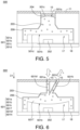
- FIG. 3 is a cross-sectional view of a partial enlargement of the structure of a light sensor 300 according to another embodiment of the present invention.
- the light sensor 300 is similar to the light sensor 200 of FIG. 2 , except that in the light sensor 300 , the light incident surface 301 a of the light guide element 301 substantially is a plane 301 c , and the light exit surface 301 b of the light guide element 301 is a single curved surface 301 d (convex surface). Since the structure of the light sensor 300 identical to that of the light sensor 200 are already disclosed above, thus will not be redundantly described here.
- FIG. 4 is a cross-sectional view of a partial enlargement of the structure of a light sensor 400 according to another embodiment of the present invention.
- the light sensor 400 is similar to the light sensor 300 of FIG. 3 , except that in the light sensor 400 , the light incident surface 401 a of the light guide element 401 further has a micro-structure 405 .
- the micro-structure 405 can be formed of a plurality of protrusions protruded from the light incident surface 401 a .
- the micro-structure 405 can be formed of a plurality of depressions depressed into the light incident surface 401 a .
- the micro-structure 405 is formed of a plurality of prisms protruded from the light incident surface 401 a .
- Each prism includes an inclined plane 405 a , which forms an angle ⁇ with the light incident surface 401 a (plane), wherein the angle ⁇ is substantially less than the incident angle ⁇ of the ambient light L perpendicular to the light incident surface 401 a.
- the micro-structure 405 is disposed on the light incident surface 401 a , which is substantially a plane, and can be neatly arranged as a convex matrix, the position, shape and arrangement of the micro-structure 405 are not limited to above exemplifications.
- the micro-structure 405 can be realized by any protrusions, depressions or a combination thereof arranged on the light incident surface 401 a and/or the light exit surface 401 b of the light guide element 401 (substantially a plane or a curved surface) in any manner.
- FIG. 5 is a cross-sectional view of a partial enlargement of the structure of a light sensor 500 according to another embodiment of the present invention.
- the light sensor 500 is similar to the light sensor 200 of FIG. 2 , except that in the light sensor 500 , the light exit surface 501 a of the light guide element 501 substantially is a single curved surface (convex surface) 501 c , and the light exit surface 501 b of the light guide element 501 is a plane 501 d . Since the structure of the light sensor 500 identical to that of the light sensor 200 are already disclosed above, thus will not be redundantly described here.
- FIG. 6 is a cross-sectional view of a partial enlargement of the structure of a light sensor 600 according to another embodiment of the present invention.
- the light sensor 600 is similar to the light sensor 200 of FIG. 2 , except that the light guide element 601 of the light sensor 600 includes a first light incident surface 601 a and a second light incident surface 601 k , wherein the first light incident surface 601 a and the second light incident surface 601 k are separated from each other and are located on the same side of the light sensor 600 or face to the same direction D 1 .
- the light guide element 601 includes a body 601 T, a first connection portion 601 M and a second connection portion 601 N.
- the light exit surface 601 b of the light guide element 601 is located at an edge under the body 601 T and faces to the optoelectronic device 202 .
- the first connection portion 601 M and the second connection portion 601 N are separated from each other and respectively are extended towards the top panel 15 of the housing 11 from the body 601 T to define a first light incident surface 601 a and a second light incident surface 601 k at the end of extension, wherein the first light incident surface 601 a and the second light incident surface 601 k are parallel to each other, face to a direction (such as direction D 1 ) perpendicular to the top panel 15 and face to the top panel 15 .
- the external ambient light L after penetrating the top panel 15 , enters the first connection portion 601 M and the second connection portion 601 N from the first light incident surface 601 a and the second light incident surface 601 k respectively, propagates to the body 601 T and then exits to the optoelectronic device 202 from the light exit surface 601 b .
- the first light incident surface 601 a and the second light incident surface 601 k a small increase in the light collection area can get an obvious expansion in the scope of light collection, so that actual state of the external ambient light L can be more accurately determined.
- FIG. 7 is a cross-sectional view of a partial enlargement of the structure of a light sensor 700 according to another embodiment of the present invention.
- the light sensor 700 is similar to the light sensor 600 of FIG. 6 with a similar structure: they both include a first light incident surface and a second light incident surface that are separated from each other.
- the light sensor 700 is different from the light sensor 600 in that the first light incident surface 701 a and the second light incident surface 701 k of the light sensor 700 are separated from each other and face towards two different directions D 1 and D 2 , wherein the directions D 1 and D 2 form an angle not equivalent to 180° (such as an angle of 90°).
- the light guide element 701 includes a body 701 T, a connection portion 701 M and a second connection portion 701 N.
- the light exit surface 701 b of the light guide element 701 is located at an edge under the body 701 T and faces to the optoelectronic device 202 .
- the first connection portion 701 M and the second connection portion 701 N are separated from each other.
- the first connection portion 701 M is extended towards the top panel 15 of the housing 11 from the body 701 T and defines a first light incident surface 701 a at the end of extension, wherein the first light incident surface 701 a faces to the direction D 1 perpendicular to the top panel 15 and faces to the top panel 15 .
- the external unidirectional ambient light L after penetrating the top panel 15 , enters the first connection portion 701 M from the first light incident surface 701 a , propagates to the body 701 T and then exits to the optoelectronic device 202 from the light exit surface 701 b.
- the second connection portion 701 N is extended towards the side panel 16 of the housing 11 from another end of the body 701 T and defines a second light incident surface 701 k at the end of extension, wherein the second light incident surface 701 k faces to the direction D 2 perpendicular to side panel 16 and faces to a side panel 16 .
- the external ambient light L after penetrating side panel 16 , enters the second connection portion 701 N from the second light incident surface 701 k , propagates to the body 701 T and then exits to the optoelectronic device 202 from the light exit surface 701 b .
- FIG. 8 is a cross-sectional view of a partial enlargement of the structure of a light sensor 800 according to another embodiment of the present invention.
- the light sensor 800 is similar to the light sensor 700 of FIG. 7 , except that the light guide element 801 of the light sensor 800 includes a first light incident surface 801 a , a second light incident surface 801 k and a third light incident surface 801 g , that are separated from each other.
- the first light incident surface 801 a and the second light incident surface 801 k are parallel with each other and face to the same direction (such as direction D 1 ); the third light incident surface 801 g is perpendicular to the first light incident surface 801 a and the second light incident surface 801 k and faces another direction (such as direction D 2 ).
- the light guide element 801 includes a body 801 T, a first connection portion 801 M, a second connection portion 801 N and a third connection portion 801 O.
- the light exit surface 801 b of the light guide element 801 is located at an edge under the body 801 T and faces to the optoelectronic device 202 .
- the first connection portion 801 M and the second connection portion 801 N are separated from each other and are respectively extended to the top panel 15 of the housing 11 from the body 801 T and respectively define a first light incident surface 801 a and a second light incident surface 801 k at the end of extension, wherein the first light incident surface 801 a and the second light incident surface 801 k are parallel to each other, face a direction D 1 perpendicular to the top panel 15 and face to the top panel 15 of the housing 11 .
- the external ambient light L after penetrating the top panel 15 , enters the first connection portion 801 M and the second connection portion 801 N from the first light incident surface 801 a and the second light incident surface 801 k respectively, propagates to the body 801 T and then exits to the optoelectronic device 202 from the light exit surface 801 b.
- the third connection portion 801 O is extended to the side panel 16 (translucent panel) of the housing 11 from the other end of the body 801 T and defines a third light incident surface 801 g at the end of extension, wherein the third light incident surface 801 g faces to the direction D 2 perpendicular to side panel 16 and is aligned with the side panel 16 .
- the external ambient light L after penetrating side panel 16 , enters the third connection portion 801 O from the third light incident surface 801 g , propagates to the body 801 T and then exits to the optoelectronic device 202 from the light exit surface 801 b .
- the scope of light collection is not limited to the same side and actual state of the external ambient light L can be more accurately determined.
- several light incident surfaces can be disposed on different edges of the body 801 T at different angles to increase the angles and the scope of light collection.
- a light sensor of an electronic device includes a light guide element and an optoelectronic device.
- the ambient light enters the light guide element from at least one light incident surface and then enters the optoelectronic device of the light sensor from single light exit surface.
Landscapes
- Physics & Mathematics (AREA)
- General Physics & Mathematics (AREA)
- Spectroscopy & Molecular Physics (AREA)
- Optics & Photonics (AREA)
- Life Sciences & Earth Sciences (AREA)
- Sustainable Development (AREA)
- Photometry And Measurement Of Optical Pulse Characteristics (AREA)
Abstract
Description
Claims (13)
Applications Claiming Priority (2)
| Application Number | Priority Date | Filing Date | Title |
|---|---|---|---|
| CN202210424314.9 | 2022-04-21 | ||
| CN202210424314.9A CN116973996A (en) | 2022-04-21 | 2022-04-21 | Photo sensor |
Publications (2)
| Publication Number | Publication Date |
|---|---|
| US20230341257A1 US20230341257A1 (en) | 2023-10-26 |
| US12123767B2 true US12123767B2 (en) | 2024-10-22 |
Family
ID=88416135
Family Applications (1)
| Application Number | Title | Priority Date | Filing Date |
|---|---|---|---|
| US17/832,774 Active 2043-01-25 US12123767B2 (en) | 2022-04-21 | 2022-06-06 | Light sensor |
Country Status (2)
| Country | Link |
|---|---|
| US (1) | US12123767B2 (en) |
| CN (1) | CN116973996A (en) |
Families Citing this family (1)
| Publication number | Priority date | Publication date | Assignee | Title |
|---|---|---|---|---|
| JP7811819B2 (en) * | 2022-06-27 | 2026-02-06 | パナソニックオートモーティブシステムズ株式会社 | display device |
Citations (27)
| Publication number | Priority date | Publication date | Assignee | Title |
|---|---|---|---|---|
| US5278929A (en) * | 1991-05-10 | 1994-01-11 | Nec Corporation | Optical module, method for fabricating the same and optical module unit with the same |
| US5495545A (en) * | 1994-10-24 | 1996-02-27 | International Business Machines Corporation | Method for extending bandwidth of large core fiber optic transmission links |
| US5953145A (en) * | 1994-04-27 | 1999-09-14 | Thomson Consumer Electronics S.A. | Multiple light path arrangement |
| US6243508B1 (en) * | 1999-06-01 | 2001-06-05 | Picolight Incorporated | Electro-opto-mechanical assembly for coupling a light source or receiver to an optical waveguide |
| US20020071459A1 (en) * | 2000-09-29 | 2002-06-13 | Kevin Malone | Apparatus and method for VCSEL monitoring using scattering and reflection of emitted light |
| US20030136650A1 (en) * | 2002-01-24 | 2003-07-24 | Che-Yi Lai | Two-stage touch switch |
| US20040109629A1 (en) * | 2002-10-01 | 2004-06-10 | Seiko Epson Corporation | Optical interconnection circuit, manufacturing method thereof, electro-optical device and electronic equipment |
| US20050124224A1 (en) * | 2003-11-03 | 2005-06-09 | Nikolaus Schunk | Adapter for connecting an optoelectronic transducer module to a printed circuit board, transmitting and/or receiving arrangement with such an adapter, optoelectronic transducer module and method for its production |
| US20050168987A1 (en) * | 1999-07-26 | 2005-08-04 | Labosphere Institute | Bulk-shaped lens, light-emitting unit, lighting equipment and optical information system |
| US20060060882A1 (en) * | 2004-09-22 | 2006-03-23 | Sharp Kabushiki Kaisha | Optical semiconductor device, optical communication device, and electronic equipment |
| CN1284011C (en) | 2003-07-18 | 2006-11-08 | 财团法人工业技术研究院 | Composite microstructure sheet for diffusing and concentrating light |
| US7625136B2 (en) * | 2006-12-18 | 2009-12-01 | Seiko Epson Corporation | Optical module and optical communication device |
| US7654750B2 (en) * | 2005-08-10 | 2010-02-02 | Brenner Mary K | Bidirectional optical fiber link systems component couplers |
| US20100239212A1 (en) * | 2009-03-20 | 2010-09-23 | Nec Electronics Corporation | Optical module |
| US20130168537A1 (en) * | 2010-09-20 | 2013-07-04 | Opticis Co., Ltd. | Apparatus for wavelength-division multiplexing and demultiplexing |
| US8809125B2 (en) * | 2005-10-18 | 2014-08-19 | Finisar Corporation | Reducing thermal expansion effects in semiconductor packages |
| US20140346333A1 (en) * | 2013-05-21 | 2014-11-27 | Omron Automotive Electronics Co., Ltd. | Photodetection device |
| US20150244465A1 (en) * | 2014-02-21 | 2015-08-27 | Optomedia Technology Inc. | Optical communication module |
| US20150268425A1 (en) * | 2012-04-20 | 2015-09-24 | Corning Cable Systems Llc | Fiber optic module assemblies and connector assemblies using the same |
| CN106662686A (en) | 2015-07-28 | 2017-05-10 | Jsr株式会社 | Optical filter and environment light sensor provided with optical filter |
| US20180014092A1 (en) * | 2015-09-14 | 2018-01-11 | Russell Tyler Martin | Controlled Signals Using Signal Guides For Sensor Devices |
| US20180330140A1 (en) * | 2014-10-23 | 2018-11-15 | Gingy Technology Inc. | Fingerprint identification apparatus |
| US10147853B2 (en) * | 2011-03-18 | 2018-12-04 | Cree, Inc. | Encapsulant with index matched thixotropic agent |
| US20190086619A1 (en) * | 2017-09-18 | 2019-03-21 | Orangetek Corporation | Optical communication module |
| US20190162389A1 (en) * | 2016-05-18 | 2019-05-30 | SMR Patents S.à.r.l. | Lens and method of producing a lens |
| CN208969540U (en) | 2018-08-29 | 2019-06-11 | 徐智 | Mini-computer |
| US20220163833A1 (en) * | 2019-10-30 | 2022-05-26 | Zte Corporation | Display screen module and terminal |
-
2022
- 2022-04-21 CN CN202210424314.9A patent/CN116973996A/en active Pending
- 2022-06-06 US US17/832,774 patent/US12123767B2/en active Active
Patent Citations (28)
| Publication number | Priority date | Publication date | Assignee | Title |
|---|---|---|---|---|
| US5278929A (en) * | 1991-05-10 | 1994-01-11 | Nec Corporation | Optical module, method for fabricating the same and optical module unit with the same |
| US5953145A (en) * | 1994-04-27 | 1999-09-14 | Thomson Consumer Electronics S.A. | Multiple light path arrangement |
| US5495545A (en) * | 1994-10-24 | 1996-02-27 | International Business Machines Corporation | Method for extending bandwidth of large core fiber optic transmission links |
| US6243508B1 (en) * | 1999-06-01 | 2001-06-05 | Picolight Incorporated | Electro-opto-mechanical assembly for coupling a light source or receiver to an optical waveguide |
| US20050168987A1 (en) * | 1999-07-26 | 2005-08-04 | Labosphere Institute | Bulk-shaped lens, light-emitting unit, lighting equipment and optical information system |
| US20020071459A1 (en) * | 2000-09-29 | 2002-06-13 | Kevin Malone | Apparatus and method for VCSEL monitoring using scattering and reflection of emitted light |
| US20030136650A1 (en) * | 2002-01-24 | 2003-07-24 | Che-Yi Lai | Two-stage touch switch |
| US20040109629A1 (en) * | 2002-10-01 | 2004-06-10 | Seiko Epson Corporation | Optical interconnection circuit, manufacturing method thereof, electro-optical device and electronic equipment |
| CN1284011C (en) | 2003-07-18 | 2006-11-08 | 财团法人工业技术研究院 | Composite microstructure sheet for diffusing and concentrating light |
| US20050124224A1 (en) * | 2003-11-03 | 2005-06-09 | Nikolaus Schunk | Adapter for connecting an optoelectronic transducer module to a printed circuit board, transmitting and/or receiving arrangement with such an adapter, optoelectronic transducer module and method for its production |
| US20060060882A1 (en) * | 2004-09-22 | 2006-03-23 | Sharp Kabushiki Kaisha | Optical semiconductor device, optical communication device, and electronic equipment |
| US7654750B2 (en) * | 2005-08-10 | 2010-02-02 | Brenner Mary K | Bidirectional optical fiber link systems component couplers |
| US8809125B2 (en) * | 2005-10-18 | 2014-08-19 | Finisar Corporation | Reducing thermal expansion effects in semiconductor packages |
| US7625136B2 (en) * | 2006-12-18 | 2009-12-01 | Seiko Epson Corporation | Optical module and optical communication device |
| US20100239212A1 (en) * | 2009-03-20 | 2010-09-23 | Nec Electronics Corporation | Optical module |
| US20130168537A1 (en) * | 2010-09-20 | 2013-07-04 | Opticis Co., Ltd. | Apparatus for wavelength-division multiplexing and demultiplexing |
| US10147853B2 (en) * | 2011-03-18 | 2018-12-04 | Cree, Inc. | Encapsulant with index matched thixotropic agent |
| US20150268425A1 (en) * | 2012-04-20 | 2015-09-24 | Corning Cable Systems Llc | Fiber optic module assemblies and connector assemblies using the same |
| US20140346333A1 (en) * | 2013-05-21 | 2014-11-27 | Omron Automotive Electronics Co., Ltd. | Photodetection device |
| US20150244465A1 (en) * | 2014-02-21 | 2015-08-27 | Optomedia Technology Inc. | Optical communication module |
| US20180330140A1 (en) * | 2014-10-23 | 2018-11-15 | Gingy Technology Inc. | Fingerprint identification apparatus |
| CN106662686A (en) | 2015-07-28 | 2017-05-10 | Jsr株式会社 | Optical filter and environment light sensor provided with optical filter |
| CN106662686B (en) | 2015-07-28 | 2020-06-23 | Jsr株式会社 | Optical filter, ambient light sensor, and electronic device |
| US20180014092A1 (en) * | 2015-09-14 | 2018-01-11 | Russell Tyler Martin | Controlled Signals Using Signal Guides For Sensor Devices |
| US20190162389A1 (en) * | 2016-05-18 | 2019-05-30 | SMR Patents S.à.r.l. | Lens and method of producing a lens |
| US20190086619A1 (en) * | 2017-09-18 | 2019-03-21 | Orangetek Corporation | Optical communication module |
| CN208969540U (en) | 2018-08-29 | 2019-06-11 | 徐智 | Mini-computer |
| US20220163833A1 (en) * | 2019-10-30 | 2022-05-26 | Zte Corporation | Display screen module and terminal |
Also Published As
| Publication number | Publication date |
|---|---|
| US20230341257A1 (en) | 2023-10-26 |
| CN116973996A (en) | 2023-10-31 |
Similar Documents
| Publication | Publication Date | Title |
|---|---|---|
| CN210573827U (en) | LCD fingerprint identification system, under-screen optical fingerprint identification device and electronic device | |
| CN208654763U (en) | Display components and electronic equipment | |
| US11294152B2 (en) | Optical device for fingerprint collection | |
| WO2019114276A1 (en) | Fingerprint recognition device, fingerprint recognition method, and display device | |
| JP4513918B2 (en) | Illumination device and electro-optical device | |
| CN109447046A (en) | Display panel and display device | |
| CN110989229B (en) | Display panel and display device | |
| US11798313B2 (en) | Fingerprint identification module and electronic device | |
| CN108875662B (en) | A display panel and display device | |
| WO2021108968A1 (en) | Under-screen optical fingerprint recognition apparatus and system, and liquid crystal display screen | |
| WO2021103888A1 (en) | Liquid crystal display apparatus | |
| TWI654916B (en) | Portable electronic device | |
| CN104141896A (en) | Light source module | |
| WO2020020125A1 (en) | Mobile terminal | |
| JP7460659B2 (en) | Display module and display device | |
| US12123767B2 (en) | Light sensor | |
| EP3979125A1 (en) | Screen fingerprint assembly and terminal device | |
| CN112689840A (en) | Electronic device | |
| WO2016192362A1 (en) | Optical touch device and operation method thereof | |
| CN211087263U (en) | Optical fingerprint identification device under screen, system and liquid crystal display screen | |
| US11493796B2 (en) | Display screen module and terminal | |
| CN213210660U (en) | Backlight module, passive light-emitting display device, under-screen biological characteristic detection system and electronic equipment | |
| CN211087267U (en) | Fingerprint identification device, backlight module, display screen and electronic equipment | |
| WO2021213005A1 (en) | Electronic device | |
| KR102199100B1 (en) | Image sensor package for finger-print and electronic device capable of detecting finger-print |
Legal Events
| Date | Code | Title | Description |
|---|---|---|---|
| AS | Assignment |
Owner name: QISDA CORPORATION, TAIWAN Free format text: ASSIGNMENT OF ASSIGNORS INTEREST;ASSIGNORS:LAI, CHE-YI;SHEN, CHUN-MING;LEE, CHIN-KUEI;AND OTHERS;REEL/FRAME:060105/0678 Effective date: 20220530 |
|
| FEPP | Fee payment procedure |
Free format text: ENTITY STATUS SET TO UNDISCOUNTED (ORIGINAL EVENT CODE: BIG.); ENTITY STATUS OF PATENT OWNER: LARGE ENTITY |
|
| STPP | Information on status: patent application and granting procedure in general |
Free format text: DOCKETED NEW CASE - READY FOR EXAMINATION |
|
| STPP | Information on status: patent application and granting procedure in general |
Free format text: NON FINAL ACTION MAILED |
|
| STPP | Information on status: patent application and granting procedure in general |
Free format text: RESPONSE TO NON-FINAL OFFICE ACTION ENTERED AND FORWARDED TO EXAMINER |
|
| STPP | Information on status: patent application and granting procedure in general |
Free format text: NOTICE OF ALLOWANCE MAILED -- APPLICATION RECEIVED IN OFFICE OF PUBLICATIONS |
|
| STPP | Information on status: patent application and granting procedure in general |
Free format text: PUBLICATIONS -- ISSUE FEE PAYMENT RECEIVED |
|
| STCF | Information on status: patent grant |
Free format text: PATENTED CASE |
|
| AS | Assignment |
Owner name: KD KNIT CORP., NEW YORK Free format text: NUNC PRO TUNC ASSIGNMENT;ASSIGNOR:KD DANCE RETAIL LLC;REEL/FRAME:070324/0712 Effective date: 20250207 |