US12123744B2 - Distance measuring device - Google Patents
Distance measuring device Download PDFInfo
- Publication number
- US12123744B2 US12123744B2 US17/436,171 US202017436171A US12123744B2 US 12123744 B2 US12123744 B2 US 12123744B2 US 202017436171 A US202017436171 A US 202017436171A US 12123744 B2 US12123744 B2 US 12123744B2
- Authority
- US
- United States
- Prior art keywords
- light
- receiving
- pixel
- shielded
- receiving pixel
- Prior art date
- Legal status (The legal status is an assumption and is not a legal conclusion. Google has not performed a legal analysis and makes no representation as to the accuracy of the status listed.)
- Active, expires
Links
Images


Classifications
-
- G—PHYSICS
- G01—MEASURING; TESTING
- G01C—MEASURING DISTANCES, LEVELS OR BEARINGS; SURVEYING; NAVIGATION; GYROSCOPIC INSTRUMENTS; PHOTOGRAMMETRY OR VIDEOGRAMMETRY
- G01C3/00—Measuring distances in line of sight; Optical rangefinders
- G01C3/02—Details
- G01C3/06—Use of electric means to obtain final indication
-
- G—PHYSICS
- G01—MEASURING; TESTING
- G01S—RADIO DIRECTION-FINDING; RADIO NAVIGATION; DETERMINING DISTANCE OR VELOCITY BY USE OF RADIO WAVES; LOCATING OR PRESENCE-DETECTING BY USE OF THE REFLECTION OR RERADIATION OF RADIO WAVES; ANALOGOUS ARRANGEMENTS USING OTHER WAVES
- G01S17/00—Systems using the reflection or reradiation of electromagnetic waves other than radio waves, e.g. lidar systems
- G01S17/88—Lidar systems specially adapted for specific applications
- G01S17/89—Lidar systems specially adapted for specific applications for mapping or imaging
- G01S17/894—3D imaging with simultaneous measurement of time-of-flight at a 2D array of receiver pixels, e.g. time-of-flight cameras or flash lidar
-
- G—PHYSICS
- G01—MEASURING; TESTING
- G01S—RADIO DIRECTION-FINDING; RADIO NAVIGATION; DETERMINING DISTANCE OR VELOCITY BY USE OF RADIO WAVES; LOCATING OR PRESENCE-DETECTING BY USE OF THE REFLECTION OR RERADIATION OF RADIO WAVES; ANALOGOUS ARRANGEMENTS USING OTHER WAVES
- G01S17/00—Systems using the reflection or reradiation of electromagnetic waves other than radio waves, e.g. lidar systems
- G01S17/88—Lidar systems specially adapted for specific applications
- G01S17/93—Lidar systems specially adapted for specific applications for anti-collision purposes
- G01S17/931—Lidar systems specially adapted for specific applications for anti-collision purposes of land vehicles
-
- G—PHYSICS
- G01—MEASURING; TESTING
- G01S—RADIO DIRECTION-FINDING; RADIO NAVIGATION; DETERMINING DISTANCE OR VELOCITY BY USE OF RADIO WAVES; LOCATING OR PRESENCE-DETECTING BY USE OF THE REFLECTION OR RERADIATION OF RADIO WAVES; ANALOGOUS ARRANGEMENTS USING OTHER WAVES
- G01S7/00—Details of systems according to groups G01S13/00, G01S15/00, G01S17/00
- G01S7/48—Details of systems according to groups G01S13/00, G01S15/00, G01S17/00 of systems according to group G01S17/00
- G01S7/491—Details of non-pulse systems
- G01S7/4912—Receivers
- G01S7/4913—Circuits for detection, sampling, integration or read-out
- G01S7/4914—Circuits for detection, sampling, integration or read-out of detector arrays, e.g. charge-transfer gates
-
- G—PHYSICS
- G01—MEASURING; TESTING
- G01S—RADIO DIRECTION-FINDING; RADIO NAVIGATION; DETERMINING DISTANCE OR VELOCITY BY USE OF RADIO WAVES; LOCATING OR PRESENCE-DETECTING BY USE OF THE REFLECTION OR RERADIATION OF RADIO WAVES; ANALOGOUS ARRANGEMENTS USING OTHER WAVES
- G01S7/00—Details of systems according to groups G01S13/00, G01S15/00, G01S17/00
- G01S7/48—Details of systems according to groups G01S13/00, G01S15/00, G01S17/00 of systems according to group G01S17/00
- G01S7/491—Details of non-pulse systems
- G01S7/4912—Receivers
- G01S7/4915—Time delay measurement, e.g. operational details for pixel components; Phase measurement
-
- H01L31/0203—
-
- H01L31/02164—
-
- H01L31/0232—
-
- H01L31/107—
-
- H—ELECTRICITY
- H10—SEMICONDUCTOR DEVICES; ELECTRIC SOLID-STATE DEVICES NOT OTHERWISE PROVIDED FOR
- H10F—INORGANIC SEMICONDUCTOR DEVICES SENSITIVE TO INFRARED RADIATION, LIGHT, ELECTROMAGNETIC RADIATION OF SHORTER WAVELENGTH OR CORPUSCULAR RADIATION
- H10F30/00—Individual radiation-sensitive semiconductor devices in which radiation controls the flow of current through the devices, e.g. photodetectors
- H10F30/20—Individual radiation-sensitive semiconductor devices in which radiation controls the flow of current through the devices, e.g. photodetectors the devices having potential barriers, e.g. phototransistors
- H10F30/21—Individual radiation-sensitive semiconductor devices in which radiation controls the flow of current through the devices, e.g. photodetectors the devices having potential barriers, e.g. phototransistors the devices being sensitive to infrared, visible or ultraviolet radiation
- H10F30/22—Individual radiation-sensitive semiconductor devices in which radiation controls the flow of current through the devices, e.g. photodetectors the devices having potential barriers, e.g. phototransistors the devices being sensitive to infrared, visible or ultraviolet radiation the devices having only one potential barrier, e.g. photodiodes
- H10F30/225—Individual radiation-sensitive semiconductor devices in which radiation controls the flow of current through the devices, e.g. photodetectors the devices having potential barriers, e.g. phototransistors the devices being sensitive to infrared, visible or ultraviolet radiation the devices having only one potential barrier, e.g. photodiodes the potential barrier working in avalanche mode, e.g. avalanche photodiodes
-
- H—ELECTRICITY
- H10—SEMICONDUCTOR DEVICES; ELECTRIC SOLID-STATE DEVICES NOT OTHERWISE PROVIDED FOR
- H10F—INORGANIC SEMICONDUCTOR DEVICES SENSITIVE TO INFRARED RADIATION, LIGHT, ELECTROMAGNETIC RADIATION OF SHORTER WAVELENGTH OR CORPUSCULAR RADIATION
- H10F77/00—Constructional details of devices covered by this subclass
- H10F77/30—Coatings
- H10F77/306—Coatings for devices having potential barriers
- H10F77/331—Coatings for devices having potential barriers for filtering or shielding light, e.g. multicolour filters for photodetectors
- H10F77/334—Coatings for devices having potential barriers for filtering or shielding light, e.g. multicolour filters for photodetectors for shielding light, e.g. light blocking layers or cold shields for infrared detectors
-
- H—ELECTRICITY
- H10—SEMICONDUCTOR DEVICES; ELECTRIC SOLID-STATE DEVICES NOT OTHERWISE PROVIDED FOR
- H10F—INORGANIC SEMICONDUCTOR DEVICES SENSITIVE TO INFRARED RADIATION, LIGHT, ELECTROMAGNETIC RADIATION OF SHORTER WAVELENGTH OR CORPUSCULAR RADIATION
- H10F77/00—Constructional details of devices covered by this subclass
- H10F77/40—Optical elements or arrangements
-
- H—ELECTRICITY
- H10—SEMICONDUCTOR DEVICES; ELECTRIC SOLID-STATE DEVICES NOT OTHERWISE PROVIDED FOR
- H10F—INORGANIC SEMICONDUCTOR DEVICES SENSITIVE TO INFRARED RADIATION, LIGHT, ELECTROMAGNETIC RADIATION OF SHORTER WAVELENGTH OR CORPUSCULAR RADIATION
- H10F77/00—Constructional details of devices covered by this subclass
- H10F77/50—Encapsulations or containers
-
- G—PHYSICS
- G01—MEASURING; TESTING
- G01C—MEASURING DISTANCES, LEVELS OR BEARINGS; SURVEYING; NAVIGATION; GYROSCOPIC INSTRUMENTS; PHOTOGRAMMETRY OR VIDEOGRAMMETRY
- G01C3/00—Measuring distances in line of sight; Optical rangefinders
- G01C3/02—Details
- G01C3/06—Use of electric means to obtain final indication
- G01C3/08—Use of electric radiation detectors
Definitions
- the present disclosure relates to a distance measuring device that measures a distance to a measurement object.
- a TOF (Time OF Flight) method is frequently used to measure a distance to a measurement object.
- this TOF method light is emitted, and reflected light reflected by the measurement object is detected. Then, in the TOF method, the distance to the measurement object is measured by measuring a time difference between a timing at which the light is emitted and a timing at which the reflected light is detected.
- PTLs 1 and 2 disclose a technology for providing a light-receiving element that detects reflected light reflected inside a module in addition to a light-receiving element that detects reflected light reflected by a measurement object (see PTLs 1 and 2, for example).
- a distance measuring device includes a light-receiving section and a processor.
- the light-receiving section includes a first light-receiving pixel and a second light-receiving pixel that are configured to detect light, and a light-shielded pixel that is light-shielded, and the first light-receiving pixel, the light-shielded pixel, and the second light-receiving pixel are disposed in this order in a first direction.
- the processor is configured to measure a distance to a measurement object on the basis of a detection result in the first light-receiving pixel and a detection result in the second light-receiving pixel.
- the first light-receiving pixel, the light-shielded pixel, and the second light-receiving pixel are disposed in this order in the first direction. Then, the distance to the measurement object is measured on the basis of the detection result in the first light-receiving pixel and the detection result in the second light-receiving pixel.
- FIG. 1 is a block diagram illustrating a configuration example of a distance measuring device according to an embodiment of the present disclosure.
- FIGS. 2 A and 2 B are explanatory diagrams illustrating a configuration example of a light-emitting section and a light-receiving section illustrated in FIG. 1 .
- FIG. 3 is a cross-sectional view of a configuration example of the light-receiving section illustrated in FIGS. 2 A and 2 B .
- FIGS. 4 A and 4 B are timing waveform diagrams illustrating an operation example of the distance measuring device illustrated in FIG. 1 .
- FIG. 5 is an explanatory diagram illustrating an operation example of the light-receiving section illustrated in FIG. 3 .
- FIG. 6 is a block diagram illustrating a configuration example of a distance measuring device according to a modification example.
- FIGS. 7 A and 7 B are explanatory diagrams illustrating a configuration example of a light-receiving section according to another modification example.
- FIG. 8 is a block diagram illustrating a configuration example of a distance measuring device according to another modification example.
- FIGS. 9 A and 9 B are explanatory diagram illustrating a configuration example of a light-emitting section and a light-receiving section illustrated in FIG. 8 .
- FIG. 10 is a cross-sectional view of a configuration example of a light-receiving section according to another modification example.
- FIG. 11 is a cross-sectional view of a configuration example of a light-receiving section according to another modification example.
- FIG. 12 is a cross-sectional view of a configuration example of a light-receiving section according to another modification example.
- FIG. 13 is an explanatory diagram illustrating an operation example of the light-receiving section illustrated in FIG. 12 .
- FIGS. 14 A and 14 B are timing waveform diagrams illustrating an operation example of a distance measuring device according to another modification example.
- FIG. 15 is a block diagram depicting an example of schematic configuration of a vehicle control system.
- FIG. 16 is a diagram of assistance in explaining an example of installation positions of an outside-vehicle information detecting section and an imaging section.
- FIG. 1 illustrates a configuration example of a distance measuring device (a distance measuring device 1 ) according to an embodiment.
- the distance measuring device 1 is configured to measure a distance to a measurement object 100 by emitting light toward the measurement object 100 , detecting light L 2 reflected by the measurement object 100 , and measuring a flight time of light on the basis of a thus-obtained detection result.
- the distance measuring device 1 is configured to measure the distance to the measurement object 100 by a direct method.
- the distance measuring device 1 includes a light-emitting section 11 , a reflecting body 12 , a light-receiving section 13 , and a processor 15 .
- the light-emitting section 11 is configured to emit light L 0 that is pulsed light from a light-emitting surface S 0 on the basis of an instruction from the processor 15 .
- the light-emitting section 11 includes, for example, a light source that emits infrared light.
- the light source is configured with use of a laser light source, an LED (Light Emitting Diode), or the like.
- the reflecting body 12 is configured to allow a portion of the light L 0 emitted from the light-emitting section 11 to pass therethrough, as well as to reflect a portion of the light L 0 .
- the reflecting body 12 is configured with use of a half mirror, for example.
- Light (light L 1 ) having passed through the reflecting body 12 travels toward the measurement object 100 , and is reflected by the measurement object 100 .
- light (light L 1 R) reflected by the reflecting body 12 travels toward the light-receiving section 13 .
- the light-receiving section 13 is configured to detect the light L 1 R reflected by the reflecting body 12 and light L 2 reflected by the measurement object 100 .
- FIGS. 2 A and 2 B illustrate a configuration example of the light-emitting section 11 and the light-receiving section 13 .
- the light-emitting section 11 and the light-receiving section 13 are disposed in an XY plane, and is provided side by side in an X direction.
- the light-emitting surface SO of the light-emitting section 11 and a light-receiving surface S 2 of the light-receiving section 13 are disposed to be directed in a Z direction.
- the light-receiving section 13 includes a pixel array A.
- the pixel array A includes a plurality of pixels P arranged in a matrix.
- Each of the plurality of pixels P includes a light-receiving element PD.
- a photodiode such as an avalanche photodiode (APD; Avalanche Photodiode) or a single photon avalanche diode (SPAD; Single Photon Avalanche Diode) for the light-receiving element PD.
- APD avalanche photodiode
- SPAD Single Photon Avalanche Diode
- the pixel P (a light-receiving pixel P 1 ) that is able to detect light is disposed in the region A 1 .
- the light-receiving pixel P 1 detects the light L 1 R reflected by the reflecting body 12 .
- one column of the light-receiving pixels P 1 provided side by side in a Y direction is disposed in the region A 1 . It is to be noted that this is not limitative, and a plurality of columns of the light-receiving pixels P 1 may be disposed.
- the pixel P (a light-shielded pixel P 2 ) that is light-shielded to prevent light from being incident thereon is disposed in the region A 2 (A 21 and A 22 ). Providing such a light-shielded pixel P 2 makes it possible for the distance measuring device 1 to measure, for example, a so-called dark current passing through the light-receiving element PD. In this example, three columns of the light-shielded pixels P 2 are disposed in each of the regions A 21 and A 22 . It is to be noted that this is not limitative, and two or less columns of the light-shielded pixels P 2 may be disposed, or four or more columns of the light-shielded pixels P 2 may be disposed.
- the pixel P (a light-receiving pixel P 3 ) that is able to detect light is disposed in the region A 3 .
- the light-receiving pixel P 3 detects the light L 2 reflected by the measurement object 100 .
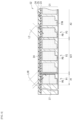
- FIG. 3 illustrates a schematic cross-sectional configuration of the light-receiving section 13 illustrated in FIGS. 2 A and 2 B as viewed from the direction of a ⁇ - ⁇ arrow.
- the light-receiving section 13 includes a semiconductor substrate 21 , a multilayer wiring layer 22 , an insulating film 23 , a light-shielding film 24 , an insulating film 25 , and a lens 26 .
- the semiconductor substrate 21 is a substrate in which an element and a circuit in the light-receiving section 13 are formed, and is a P-type semiconductor substrate in this example.
- the semiconductor substrate 21 is provided with a plurality of N-type semiconductor regions 21 N.
- the N-type semiconductor regions 21 N are formed widely in the Z direction in the semiconductor substrate 21 .
- the N-type semiconductor region 21 N and a portion of the semiconductor substrate 21 on side of the light-receiving surface S 2 as viewed from the N-type semiconductor regions 21 N are included in the light-receiving element PD.
- a plurality of MOS transistors TR is provided on a surface, on side opposite to the light receiving surface S 2 , of the semiconductor substrate 21 .
- the multilayer wiring layer 22 is provided on a surface, on side opposite to the light-receiving surface S 2 , of the semiconductor substrate 21 .
- the multilayer wiring layer 22 includes a plurality of wiring lines 22 A, and an interlayer insulating film that insulates the plurality of wiring lines 22 A from each other.
- the insulating film 23 is a film serving as an antireflective film, and is provided on side of the light-receiving surface S 2 of the semiconductor substrate 21 . It is possible to configure the insulating film 23 with use of, for example, a material such as silicon nitride (Si 3 N 4 ), hafnium oxide (HfO 2 ), aluminum oxide (Al 2 O 3 ), zirconium oxide (ZrO 2 ), tantalum oxide (Ta 2 O 5 ), titanium oxide (TiO 2 ), lanthanum oxide (La 2 O 3 ), praseodymium oxide (Pr 2 O 3 ), cerium oxide (CeO 2 ), neodymium oxide (Nd 2 O 3 ), promethium oxide (Pm 2 O 3 ), samarium oxide (Sm 2 O 3 ), europium oxide (Eu 2 O 3 ), gadolinium oxide (Gd 2 O 3 ), terbium oxide (Tb 2 O 3 ), dyspros
- the light-shielding film 24 is a film that shields light to prevent light from entering the semiconductor substrate 21 , and is provided on the insulating film 23 . Specifically, the light-shielding film 24 is provided in the region A 2 (A 21 and A 22 ), between a plurality of pixels P (the light-receiving pixels P 1 ) in the region A 1 , and between a plurality of pixels P (the light-receiving pixels P 3 ) in the region A 3 . It is possible to configure the light-shielding film 24 with use of various materials that are able to shield light.
- the light-shielding film 24 with use of, for example, metal such as tungsten (W), aluminum (Al), or copper (Cu), a resin including a coloring agent such as a pigment or a dye used for a block color filter.
- metal such as tungsten (W), aluminum (Al), or copper (Cu)
- a resin including a coloring agent such as a pigment or a dye used for a block color filter.
- the insulating film 25 is a film serving as a planarization film, and is provided on the light-shielding film 24 and the insulating film 23 .
- the lens 26 is provided on the insulating film 25 .
- the lens 26 is formed with use of, for example, an organic material such as a resin.
- the pixels P each include the light-receiving element PD, the MOS transistor TR, and the lens 26 .
- the light-receiving element PD of the light-receiving pixel P 1 , the light-receiving element PD of the light-shielded pixel P 2 , and the light-receiving element PD of the light-receiving pixel P 3 have configurations similar to each other.
- the pixel P including one MOS transistor TR is illustrated, but this is not limitative.
- the pixel P may include a plurality of MOS transistors TR.
- the light-shielding film 24 is provided in the region A 21 . This prevents light from entering the light-shielded pixel P 2 .
- a trench may be provided between adjacent light-receiving pixels P 3 in the region A 3 . This makes it possible to suppress color mixture.
- a trench may be provided between adjacent light-shielded pixels P 2 in the region A 2 . This makes it possible to determine the reference of a black level more accurately.
- the insulating film 23 may be provided inside these trenches.
- a light-shielding wall 27 is provided between the region A 1 and the region A 21 .
- the light-shielding wall 27 is configured to be provided in a standing manner in the Z direction.
- the light-shielding wall 27 may be configured to reflect light, or may be configured to absorb light.
- the light-shielding wall 27 is formed to penetrate both surfaces of the semiconductor substrate 21 . In a case where a trench is provided between adjacent light-receiving pixels P 3 or between adjacent light-shielded pixels P 2 , it is desirable that the light-shielding wall 27 have a depth equal to or larger than a depth of the trench.
- the light-shielding wall 27 is formed over a plurality of pixels P provided side by side in the Y direction along a boundary between the region A 1 and the region A 2 .
- the light-shielding wall 27 is configured to reflect light
- metal such as tungsten (W), aluminum (Al), or copper (Cu).
- W tungsten
- Al aluminum
- Cu copper
- various configurations may be used that makes it possible to totally reflect light at an interface between the semiconductor substrate 21 and the trench.
- no metal may be evaporated.
- the light-shielding wall 27 is configured to absorb light
- the processor 15 ( FIG. 1 ) is configured to perform control to cause the light-emitting section 11 to emit the light L 0 , as well as to measure a distance to the measurement object 100 in units of the light-receiving pixels P 3 by measuring a flight time of light on the basis of detection results in the light-receiving pixels P 1 in the region A 1 and the light-receiving pixels P 3 in the region A 3 in the light-receiving section 13 .
- the processor 15 measures a time from a timing at which the light-receiving pixel P 1 receives the light L 1 R to a timing at which the light-receiving pixel P 3 receives the light L 2 to measure the distance to the measurement object 100 in units of the light-receiving pixels P 3 .
- the processor 15 may measure a time from an instruction timing at which the light-emitting section 11 is instructed to emit the light L 0 to a timing at which the light-receiving pixel P 1 receives the light L 1 R and measure a time from the instruction timing to a timing at which the light-receiving pixel P 3 receives the light L 2 to measure the distance to the measurement object 100 in units of the light-receiving pixels P 3 on the basis of a difference between these times.
- a light diffusion member, n optical filter such as a bandpass filter, a lens, or any other optical member may be appropriately provided in an optical path until light emitted from the light-emitting section 11 is reflected by the measurement object 100 and the reflected light is detected by the light-receiving section 13 .
- a light diffusion member, an optical filter such as a bandpass filter, a lens, or any other optical member may be appropriately provided in an optical path until light emitted from the light-emitting section 11 is reflected by the reflecting body 12 and the reflected light is detected by the light-receiving section 13 .
- the light-receiving pixel P 1 corresponds to a specific example of a “first light-receiving pixel” in the present disclosure.
- the light-receiving pixel P 3 corresponds to a specific example of a “second light-receiving pixel” in the present disclosure.
- the light-shielded pixel P 2 corresponds to a specific example of a “light-shielded pixel” in the present disclosure.
- the light-shielding wall 27 corresponds to a specific example of a “light-shielding wall” in the present disclosure.
- the light-shielding film 24 corresponds to a specific example of a “light-shielding film” and an “inter-pixel light-shielding film” in the present disclosure.
- the reflecting body 12 corresponds to a specific example of a “light guide member” in the present disclosure.
- the light-emitting section 11 emits the light L 0 on the basis of an instruction from the processor 15 .
- the reflecting body 12 allows a portion of the light L 0 emitted from the light-emitting section 11 to pass therethrough, and reflects a portion of the light L 0 .
- the light L 1 having passed through the reflecting body 12 travels toward the measurement object 100 , and is reflected by the measurement object 100 .
- the light L 1 R reflected by the reflecting body 12 travels toward each of the light-receiving pixels P 1 in the region A 1 of the light-receiving section 13 .
- the light L 2 reflected by the measurement object 100 travels toward each of the light-receiving pixels P 3 in the region A 3 of the light-receiving section 13 .
- Each of the light-receiving pixels P 1 in the region A 1 of the light-receiving section 13 detects the light L 1 R, and each of the light-receiving pixels P 3 in the region A 3 of the light-receiving section 13 detects the light L 2 .
- the processor 15 measures a flight time of light on the basis of the detection results in the light-receiving pixels P 1 and the light-receiving pixels P 3 in the light-receiving section 13 to measure a distance to the measurement object 100 in units of the light-receiving pixels P 3 .
- FIGS. 4 A and 4 B illustrate an example of a distance measurement operation in the distance measuring device 1 .
- the distance measuring device 1 measures a distance to the measurement object 100 by a so-called direct method.
- FIG. 4 A indicates a waveform of the light L 0 emitted from the light-emitting section 11
- FIG. 4 B indicates a waveform of the light L 2 detected by the light-receiving section 13 .
- the light-emitting section 11 emits the light L 0 having a pulse waveform on the basis of an instruction from the processor 15 of FIG. 4 A ).
- the light L 0 enters the reflecting body 12 , and the light L 1 having passed through the reflecting body 12 travels toward the measurement object 100 .
- the light L 1 is reflected by the measurement object 100 , and the reflected light L 2 travels toward the light-receiving section 13 .
- the light-receiving pixel P 3 in the region A 3 of the light-receiving section 13 detects the light L 2 of FIG. 4 B ).
- the light L 2 detected by the light-receiving pixel P 3 has a waveform delayed by a delay time DL with respect to the waveform of the light L 0 illustrated in of FIG. 4 A .
- the delay time DL is a time in which light travels in order of the light-emitting section 11 , the reflecting body 12 , the measurement object 100 , and the light-receiving section 13 , and corresponds to a flight time of light.
- the flight time of light corresponds to a distance between the distance measuring device 1 and the measurement object 100 .
- the light-receiving pixel P 1 in the region A 1 of the light-receiving section 13 detects the light L 1 R of FIG. 4 B ).
- the waveform of the light L 1 R detected by the light-receiving pixel P 1 is substantially similar to the waveform of the light L 0 illustrated in of FIG. 4 A , for example.
- the processor 15 measures a time from a timing at which the light-receiving pixel P 1 receives the light L 1 R to a timing at which the light-receiving pixel P 3 receives the light L 2 .
- the distance measuring device 1 makes it possible for the distance measuring device 1 to remove an influence of circuit delay in the light-emitting section 11 , the light-receiving section 13 , and the processor 15 and to measure the flight time of light more accurately. This makes it possible for the distance measuring device 1 to measure the distance to the measurement object 100 .
- FIG. 5 illustrates an example of a light detection operation in the light-receiving section 13 . It is to be noted that FIG. 5 simply illustrates the light-receiving section 13 for convenience of description. In this example, the light L 1 R reflected by the reflecting body 12 and the light L 2 reflected by the measurement object 100 enter the light-receiving section 13 . It is to be noted that FIG. 5 illustrates the light L 1 R and the light L 2 , but the light L 1 R and the light L 2 generally enter the light-receiving section 13 at timings different from each other.
- light having entered the light-receiving element PD of the light-receiving pixel P 1 is reflected or absorbed by the light-shielding wall 27 , thereby hindering leakage of the light L 1 R from the light-receiving pixel P 1 .
- the light-shielding wall 27 is configured to reflect light, it is possible to gain an optical path length, which makes it possible to detect the light L 1 R more effectively.
- the light-receiving element PD of the light-shielded pixel P 2 in the region A 21 is light-shielded by the light-shielding wall 27 and the light-shielding film 24 , which prevents the light L 1 R from entering the light-receiving element PD of the light-shielded pixel P 2 .
- the light-receiving pixel P 1 that detects the light L 1 R and the light-receiving pixel P 3 that detects the light L 2 are separated from each other, which makes it possible to reduce a possibility that the light L 1 R enters the light-receiving element PD of the light-receiving pixel P 3 .
- the light-receiving element PD of the light-receiving pixel P 3 in the region A 3 of the light-receiving section 13 detects the light L 2 .
- the light-receiving element PD of the light-shielded pixel P 2 in the region A 21 is light-shielded by the light-shielding film 24 , which makes it possible to reduce a possibility that the light L 2 enters the light-receiving element PD of the light-shielded pixel P 2 .
- the light-receiving pixel P 1 that detects the light L 1 R and the light-receiving pixel P 3 that detects the light L 2 are separated from each other, which makes it possible to reduce a possibility that the light L 2 enters the light-receiving element PD of the light-receiving pixel P 1 .
- the light-shielded pixel P 2 is provided between the light-receiving pixel P 1 that detects the light L 1 R and the light-receiving pixel P 3 that detects the light L 2 to separate the position of the light-receiving pixel P 1 in the region A 1 and the position of the light-receiving pixel P 3 in the region A 3 from each other.
- the distance measuring device 1 it is possible to more accurately detect a timing at which the light-receiving pixel P 1 receives the light L 1 R and a timing at which the light-receiving pixel P 3 receives the light L 2 , thus making it possible to enhance measurement accuracy.
- the light-shielded pixel P 2 is provided between the light-receiving pixel P 1 that detects the light L 1 R and the light-receiving pixel P 3 that detects the light L 2 , which makes it possible to provide the light-shielded pixel P 2 while effectively using a limited area.
- the light-shielding wall 27 is provided between the light-receiving pixel P 1 in the region A 1 and the light-shielded pixel P 2 in the region A 21 . Accordingly, light, which has entered the light-receiving element PD of the light-receiving pixel P 1 , of the light L 1 R is reflected by the light-shielding wall 27 , thereby hindering leakage of the light L 1 R from the light-receiving pixel P 1 , which makes it possible for the light-receiving element PD of the light-receiving pixel P 1 to effectively detect the light L 1 R. This makes it possible for the distance measuring device 1 to more accurately detect a timing at which the light-receiving pixel P 1 receives the light L 1 R, thus making it possible to enhance measurement accuracy.
- the light-shielded pixel P 2 is provided between the light-receiving pixel P 1 that detects the light L 1 R and the light-receiving pixel P 3 that detects the light L 2 , which makes it possible to enhance measurement accuracy.
- the light-shielding wall 27 is provided between the light-receiving pixel P 1 in the region A 1 and the light-shielded pixel P 2 in the region A 21 , which makes it possible to enhance measurement accuracy.
- a reflecting body 12 A is configured with use of a half mirror, but this is not limitative, and a mirror, an optical fiber, a lens, or the like may be used.
- a reflecting body may be configured with use of glass, plastic, or the like provided between the light-emitting section and the light-receiving section.
- FIGS. 7 A and 7 B illustrate a configuration example of a distance measuring device 1 A in a case where a reflecting body is configured with use of a mirror.
- the distance measuring device 1 A includes a light-emitting section 11 A and the reflecting body 12 A.
- the light-emitting section 11 A is configured to emit the light L 0 that is pulsed light from the light-emitting surface SO on the basis of an instruction from the processor 15 .
- the light-emitting section 11 A includes, for example, a plurality of light sources.
- the reflecting body 12 A is configured to reflect the light L 0 emitted from some light sources of the plurality of light sources of the light-emitting section 11 A.
- the reflecting body 12 A is configured with use of a reflector, for example.
- the reflecting body 12 A corresponds to a specific example of a “light guide member” in the present disclosure.
- the light L 1 R reflected by the reflecting body 12 A travels toward the light-receiving section 13 . Of the light L 0 emitted from the light-emitting section 11 A, light that does not enter the reflecting body 12 A travels as the light L 1 toward the measurement object 100 .
- one column of the pixels P (the light-receiving pixels P 1 ) is provided in the region A 1 , but this is not limitative. Instead of this, for example, a plurality of columns of the pixels P may be provided in the region A 1 .
- a smaller number of the pixels P than the number of the pixels P in one column may be provided. In this example, four light-receiving pixels P 1 are provided.
- each light-receiving pixels P 1 are collectively disposed around an end in a direction opposite to the Y direction (bottom side in FIGS. 7 A and 7 B ), but this is not limitative.
- the light-receiving pixels P 1 may be disposed around the middle in the Y direction, or may be collectively disposed around an end in the Y direction (top side in FIGS. 7 A and 7 B ).
- one light-emitting section 11 is provided, but this is not limitative. Instead of this, a plurality of light-emitting sections 11 may be provided. An example in which two light-emitting sections are provided is described in detail below.
- FIG. 8 illustrates a configuration example of a distance measuring device 1 C according to the present modification example.
- the distance measuring device 1 C includes light-emitting sections 41 A and 41 B, reflecting bodies 42 A and 42 B, a light-receiving section 43 , and a processor 45 .
- the reflecting body 42 A is configured to allow a portion of the light L 0 A emitted from the light-emitting section 41 to pass therethrough, as well as to reflect a portion of the light L 0 A.
- Light (light L 1 A) having passed through the reflecting body 42 A travels toward the measurement object 100 , and is reflected by the measurement object 100 .
- light (light L 1 RA) reflected by the reflecting body 42 A travels toward the light-receiving section 43 .
- the reflecting body 42 B is configured to allow a portion of the light L 0 B emitted from the light-emitting section 41 to pass therethrough, as well as to reflect a portion of the light L 0 B.
- Light (light L 1 B) having passed through the reflecting body 42 B travels toward the measurement object 100 , and is reflected by the measurement object 100 .
- light (light L 1 RB) reflected by the reflecting body 42 B travels toward the light-receiving section 43 .
- the light-receiving section 43 is configured to detect the light L 1 RA reflected by the reflecting body 42 A, the light L 1 RB reflected by the reflecting body 42 B, and the light L 2 reflected by the measurement object 100 .
- FIGS. 9 A and 9 B illustrate a configuration example of the light-emitting sections 41 A and 41 B and the light-receiving section 43 .
- the light-emitting section 41 A, the light-receiving section 43 , and the light-emitting section 41 B are disposed in an XY plane, and is provided side by side in the X direction in this order.
- the light-emitting surface S 0 A of the light-emitting section 41 A, the light-emitting surface SOB of the light-emitting section 41 B, and the light-receiving surface S 2 of the light-receiving section 43 are disposed to be directed in the Z direction.
- the pixel array A is divided into a plurality of regions A 1 (A 11 and A 12 ), A 2 (A 21 and A 22 ), and A 3 .
- the plurality of regions A 11 , A 21 , A 3 , A 22 , and A 12 is disposed in the X direction in this order.
- the light-receiving pixel P 1 is disposed in the region A 1 (A 11 and A 12 ).
- the light-receiving pixel P 1 disposed in the region A 11 detects the light L 1 RA reflected by the reflecting body 42 A
- the light-receiving pixel P 1 disposed in the region A 12 detects the light L 1 RB reflected by the reflecting body 42 B.
- one column of the pixels P (the light-receiving pixels P 1 ) is provided in each of the regions A 11 and A 12 , but this is not limitative.
- a smaller number of the pixels P than the number of the pixels P in one column may be provided in the region A 11 .
- a smaller number of the pixels P than the number of the pixels P in one column may be provided in the region A 12 .
- a smaller number of the pixels P than the number of the pixels P in one column may be provided in each of the region A 11 and A 12 .
- the processor 45 ( FIG. 1 ) performs control to cause the light-emitting section 41 A to emit the light L 0 A, and performs control to cause the light-emitting section 41 B to emit the light L 0 B.
- the processor 45 measures a flight time of light on the basis of a detection result in the light-receiving pixel P 3 of the light-receiving section 43 to measure a distance to the measurement object 100 in units of the light-receiving pixels P 3 .
- the light-receiving element PD of the light-receiving pixel P 1 has a configuration similar to those of the light-receiving element PD of the light-receiving pixel P 3 and the light-receiving element PD of the light-shielded pixel P 2 , but this is not limitative.
- the present modification example is described below with reference to some examples.
- the light-receiving element PD of the light-receiving pixel P 1 may have a width in the X direction that is different from a width in the X direction of the light-receiving element PD of the light-receiving pixel P 3 and a width in the X direction of the light-receiving element PD of the light-shielded pixel P 2 .
- the width in the X direction of the light-receiving element PD of the light-receiving pixel P 1 is narrower than the width in the X direction of the light-receiving element PD of the light-receiving pixel P 3 and the width in the X direction of the light-receiving element PD of the light-shielded pixel P 2 , but this is not limitative.
- the width in the X direction of the light-receiving element PD of the light-receiving pixel P 1 may be wider than the width in the X direction of the light-receiving element PD of the light-receiving pixel P 3 and the width in the X direction of the light-receiving element PD of the light-shielded pixel P 2 .
- the light-receiving element PD of the light-receiving pixel P 1 may have a thickness in the Z direction that is different from a thickness in the Z direction of the light-receiving element PD of the light-receiving pixel P 3 and a thickness in the Z direction of the light-receiving element PD of the light-shielded pixel P 2 .
- the thickness in the Z direction of the light-receiving element PD of the light-receiving pixel P 1 is thinner than the thickness in the Z direction of the light-receiving element PD of the light-receiving pixel P 3 and the thickness in the Z direction of the light-receiving element PD of the light-shielded pixel P 2 .
- the light-shielding film 24 provided in the region A 21 has a thickness equal to a thickness of the light-shielding film 24 provided between the plurality of pixels P (the light-receiving pixels P 1 ) in the region A 1 and a thickness of the light-shielding film 24 provided between the plurality of pixels P (the light-receiving pixels P 3 ) in the region A 3 , but this is not limitative.
- a distance measuring device 1 F according to the present modification example is described in detail below.
- the light-shielding film 24 F is provided in the region A 2 (A 21 and A 22 ).
- the light-shielding film 24 is provided between the plurality of pixels P (the light-receiving pixels P 1 ) in the region A 1 , and between the plurality of pixels P (the light-receiving pixels P 3 ) in the region A 3 .
- the light-shielding film 24 F is formed to have a larger thickness than the light-shielding film 24 .
- the light-shielding film 24 F corresponds to a specific example of a “light-shielding film” in the present disclosure.
- the light-shielding film 24 corresponds to a specific example of an “inter-pixel light-shielding film” in the present disclosure.
- FIG. 13 illustrates an example of a light detection operation in the light-receiving section 13 F. It is to be noted that FIG. 13 simply illustrates the light-receiving section 13 F for convenience of description.
- the light L 1 R reflected by the reflecting body 12 enters the light-receiving section 13 F.
- light having entered the light-receiving element PD of the light-receiving pixel P 1 is reflected by the light-shielding wall 27 , thereby hindering leakage of the light L 1 R from the light-receiving pixel P 1 .
- the light-shielding film 24 F includes metal
- the light-shielding film 24 F is thick; therefore, partial light of the light L 1 R is reflected by a side surface of the light-shielding film 24 F and enters the light-receiving element PD of the light-receiving pixel P 1 in the region A 1 .
- the light-receiving element PD of the light-shielded pixel P 2 in the region A 21 is light-shielded by the light-shielding wall 27 and the light-shielding film 24 F; therefore, the light L 1 R does not enter the light-receiving element PD of the light-shielded pixel P 2 .
- the light-receiving pixel P 1 that detects the light L 1 R and the light-receiving pixel P 3 that detects the light L 2 are separated from each other, which makes it possible to reduce a possibility that the light L 1 R enters the light-receiving element PD of the light-receiving pixel P 3 . This makes it possible for the distance measuring device 1 F to reduce a possibility that the light-receiving pixel P 3 in the region A 3 detects the light L 1 R, thus making it possible to enhance measurement accuracy.
- the light-receiving element PD of the light-receiving pixel P 3 detects the light L 2 .
- the light-receiving element PD of the light-shielded pixel P 2 in the region A 21 is light-shielded by the light-shielding film 24 F, which makes it possible to reduce a possibility that the light L 2 enters the light-receiving element PD of the light-shielded pixel P 2 .
- the light-shielding film 24 F is thick; therefore, a portion of the light L 2 is blocked by the side surface of the light-shielding film 24 F, which makes it possible to reduce a possibility that the light L 2 enters the light-receiving element PD of the light-receiving pixel P 1 .
- the distance to the measurement object 100 is measured by the direct method, but this is not limitative. Instead of this, for example, the distance to the measurement object 100 may be measured by an indirect method, for example.
- a distance measuring device 1 H according to the present modification example includes the light-emitting section 11 , the reflecting body 12 , a light-receiving section 13 H, and a processor 15 H, as with the distance measuring device 1 ( FIG. 1 ) according to the embodiment described above.
- FIGS. 14 A and 14 B illustrate an example of a distance measurement operation in the distance measuring device 1 H according to the present modification example, where FIG. 14 A indicates the waveform of the light L 0 emitted from the light-emitting section 11 , and FIG. 14 B indicates the waveform of the light L 2 detected by the light-receiving section 13 H.
- the light-emitting section 11 emits the light L 0 having a pulse waveform with a duty ratio of 50% on the basis of an instruction from the processor 15 H FIG. 14 A ).
- the light L 0 enters the reflecting body 12 , and the light L 1 having passed through the reflecting body 12 travels toward the measurement object 100 .
- the light L 1 is reflected by the measurement object 100 , and the reflected light L 2 travels toward the light-receiving section 13 H.
- the light-receiving pixel P 3 in the region A 3 of the light-receiving section 13 H detects the light L 2 FIG. 14 B ).
- the light L 2 detected by the light-receiving pixel P 3 has a waveform delayed by a delay time DL with respect to the waveform of the light L 0 illustrated in FIG. 14 A .
- the delay time DL is a time in which light travels in order of the light-emitting section 11 , the reflecting body 12 , the measurement object 100 , and the light-receiving section 13 H, and corresponds to a flight time of light.
- the flight time of light corresponds to a distance between the distance measuring device 1 H and the measurement object 100 .
- the light-receiving pixel P 1 in the region A 1 of the light-receiving section 13 detects the light L 1 R.
- the waveform of the light L 1 R detected by the light-receiving pixel P 1 is substantially similar to the waveform of the light L 0 illustrated in FIG. 14 A , for example.
- the light-receiving pixel P 3 accumulates signal electric charges Q 1 corresponding to an amount of light received by the light-receiving element PD in a period T 1 in which the light-receiving pixel P 1 detects light, and accumulates signal electric charges Q 2 corresponding to the amount of light received by the light-receiving element PD in a period T 2 in which the light-receiving pixel P 1 does not detect light.
- the processor 15 H determines an electric charge ratio between the signal electric charges Q 1 and the signal electric charges Q 2 .
- the light-receiving element PD receives the light L 2 in the periods TA and TB; therefore, the electric charge amount of the signal electric charges Q 1 is proportional to the length of the period TA, and the electric charge amount of the signal electric charges Q 2 is proportional to the length of the period TB.
- the delay time DL is short, the signal electric charges Q 1 are increased and the signal electric charges Q 2 are decreased.
- the delay time DL is long, the signal electric charges Q 1 are decreased, and the signal electric charges Q 2 are increased.
- the electric charge ratio between the signal electric charges Q 1 and the signal electric charges Q 2 is changed depending on the delay time DL.
- determining the electric charge ratio makes it possible to determine the delay time DL with high accuracy, for example. As a result, it is possible to measure the distance to the measurement object 100 with high accuracy.
- the technology (the present technology) according to the present disclosure is applicable to various products.
- the technology according to the present disclosure may be achieved as a device mounted on any type of mobile body such as an automobile, an electric vehicle, a hybrid electric vehicle, a motorcycle, a bicycle, a personal mobility, an airplane, a drone, a vessel, and a robot.
- FIG. 15 is a block diagram depicting an example of schematic configuration of a vehicle control system as an example of a mobile body control system to which the technology according to an embodiment of the present disclosure can be applied.
- the vehicle control system 12000 includes a plurality of electronic control units connected to each other via a communication network 12001 .
- the vehicle control system 12000 includes a driving system control unit 12010 , a body system control unit 12020 , an outside-vehicle information detecting unit 12030 , an in-vehicle information detecting unit 12040 , and an integrated control unit 12050 .
- a microcomputer 12051 , a sound/image output section 12052 , and a vehicle-mounted network interface (I/F) 12053 are illustrated as a functional configuration of the integrated control unit 12050 .
- the driving system control unit 12010 controls the operation of devices related to the driving system of the vehicle in accordance with various kinds of programs.
- the driving system control unit 12010 functions as a control device for a driving force generating device for generating the driving force of the vehicle, such as an internal combustion engine, a driving motor, or the like, a driving force transmitting mechanism for transmitting the driving force to wheels, a steering mechanism for adjusting the steering angle of the vehicle, a braking device for generating the braking force of the vehicle, and the like.
- the body system control unit 12020 controls the operation of various kinds of devices provided to a vehicle body in accordance with various kinds of programs.
- the body system control unit 12020 functions as a control device for a keyless entry system, a smart key system, a power window device, or various kinds of lamps such as a headlamp, a backup lamp, a brake lamp, a turn signal, a fog lamp, or the like.
- radio waves transmitted from a mobile device as an alternative to a key or signals of various kinds of switches can be input to the body system control unit 12020 .
- the body system control unit 12020 receives these input radio waves or signals, and controls a door lock device, the power window device, the lamps, or the like of the vehicle.
- the outside-vehicle information detecting unit 12030 detects information about the outside of the vehicle including the vehicle control system 12000 .
- the outside-vehicle information detecting unit 12030 is connected with an imaging section 12031 .
- the outside-vehicle information detecting unit 12030 makes the imaging section 12031 image an image of the outside of the vehicle, and receives the imaged image.
- the outside-vehicle information detecting unit 12030 may perform processing of detecting an object such as a human, a vehicle, an obstacle, a sign, a character on a road surface, or the like, or processing of detecting a distance thereto.
- the imaging section 12031 is an optical sensor that receives light, and which outputs an electric signal corresponding to a received light amount of the light.
- the imaging section 12031 can output the electric signal as an image, or can output the electric signal as information about a measured distance.
- the light received by the imaging section 12031 may be visible light, or may be invisible light such as infrared rays or the like.
- the in-vehicle information detecting unit 12040 detects information about the inside of the vehicle.
- the in-vehicle information detecting unit 12040 is, for example, connected with a driver state detecting section 12041 that detects the state of a driver.
- the driver state detecting section 12041 for example, includes a camera that images the driver.
- the in-vehicle information detecting unit 12040 may calculate a degree of fatigue of the driver or a degree of concentration of the driver, or may determine whether the driver is dozing.
- the microcomputer 12051 can calculate a control target value for the driving force generating device, the steering mechanism, or the braking device on the basis of the information about the inside or outside of the vehicle which information is obtained by the outside-vehicle information detecting unit 12030 or the in-vehicle information detecting unit 12040 , and output a control command to the driving system control unit 12010 .
- the microcomputer 12051 can perform cooperative control intended to implement functions of an advanced driver assistance system (ADAS) which functions include collision avoidance or shock mitigation for the vehicle, following driving based on a following distance, vehicle speed maintaining driving, a warning of collision of the vehicle, a warning of deviation of the vehicle from a lane, or the like.
- ADAS advanced driver assistance system
- the microcomputer 12051 can perform cooperative control intended for automatic driving, which makes the vehicle to travel autonomously without depending on the operation of the driver, or the like, by controlling the driving force generating device, the steering mechanism, the braking device, or the like on the basis of the information about the outside or inside of the vehicle which information is obtained by the outside-vehicle information detecting unit 12030 or the in-vehicle information detecting unit 12040 .
- the microcomputer 12051 can output a control command to the body system control unit 12020 on the basis of the information about the outside of the vehicle which information is obtained by the outside-vehicle information detecting unit 12030 .
- the microcomputer 12051 can perform cooperative control intended to prevent a glare by controlling the headlamp so as to change from a high beam to a low beam, for example, in accordance with the position of a preceding vehicle or an oncoming vehicle detected by the outside-vehicle information detecting unit 12030 .
- the sound/image output section 12052 transmits an output signal of at least one of a sound and an image to an output device capable of visually or auditorily notifying information to an occupant of the vehicle or the outside of the vehicle.
- an audio speaker 12061 a display section 12062 , and an instrument panel 12063 are illustrated as the output device.
- the display section 12062 may, for example, include at least one of an on-board display and a head-up display.
- FIG. 16 is a diagram depicting an example of the installation position of the imaging section 12031 .
- the imaging section 12031 includes imaging sections 12101 , 12102 , 12103 , 12104 , and 12105 .
- the imaging sections 12101 , 12102 , 12103 , 12104 , and 12105 are, for example, disposed at positions on a front nose, sideview mirrors, a rear bumper, and a back door of the vehicle 12100 as well as a position on an upper portion of a windshield within the interior of the vehicle.
- the imaging section 12101 provided to the front nose and the imaging section 12105 provided to the upper portion of the windshield within the interior of the vehicle obtain mainly an image of the front of the vehicle 12100 .
- the imaging sections 12102 and 12103 provided to the sideview mirrors obtain mainly an image of the sides of the vehicle 12100 .
- the imaging section 12104 provided to the rear bumper or the back door obtains mainly an image of the rear of the vehicle 12100 .
- the imaging section 12105 provided to the upper portion of the windshield within the interior of the vehicle is used mainly to detect a preceding vehicle, a pedestrian, an obstacle, a signal, a traffic sign, a lane, or the like.
- FIG. 16 depicts an example of photographing ranges of the imaging sections 12101 to 12104 .
- An imaging range 12111 represents the imaging range of the imaging section 12101 provided to the front nose.
- Imaging ranges 12112 and 12113 respectively represent the imaging ranges of the imaging sections 12102 and 12103 provided to the sideview mirrors.
- An imaging range 12114 represents the imaging range of the imaging section 12104 provided to the rear bumper or the back door.
- a bird's-eye image of the vehicle 12100 as viewed from above is obtained by superimposing image data imaged by the imaging sections 12101 to 12104 , for example.
- At least one of the imaging sections 12101 to 12104 may have a function of obtaining distance information.
- at least one of the imaging sections 12101 to 12104 may be a stereo camera constituted of a plurality of imaging elements, or may be an imaging element having pixels for phase difference detection.
- the microcomputer 12051 can determine a distance to each three-dimensional object within the imaging ranges 12111 to 12114 and a temporal change in the distance (relative speed with respect to the vehicle 12100 ) on the basis of the distance information obtained from the imaging sections 12101 to 12104 , and thereby extract, as a preceding vehicle, a nearest three-dimensional object in particular that is present on a traveling path of the vehicle 12100 and which travels in substantially the same direction as the vehicle 12100 at a predetermined speed (for example, equal to or more than 0 km/hour). Further, the microcomputer 12051 can set a following distance to be maintained in front of a preceding vehicle in advance, and perform automatic brake control (including following stop control), automatic acceleration control (including following start control), or the like. It is thus possible to perform cooperative control intended for automatic driving that makes the vehicle travel autonomously without depending on the operation of the driver or the like.
- automatic brake control including following stop control
- automatic acceleration control including following start control
- the microcomputer 12051 can classify three-dimensional object data on three-dimensional objects into three-dimensional object data of a two-wheeled vehicle, a standard-sized vehicle, a large-sized vehicle, a pedestrian, a utility pole, and other three-dimensional objects on the basis of the distance information obtained from the imaging sections 12101 to 12104 , extract the classified three-dimensional object data, and use the extracted three-dimensional object data for automatic avoidance of an obstacle.
- the microcomputer 12051 identifies obstacles around the vehicle 12100 as obstacles that the driver of the vehicle 12100 can recognize visually and obstacles that are difficult for the driver of the vehicle 12100 to recognize visually. Then, the microcomputer 12051 determines a collision risk indicating a risk of collision with each obstacle.
- the microcomputer 12051 In a situation in which the collision risk is equal to or higher than a set value and there is thus a possibility of collision, the microcomputer 12051 outputs a warning to the driver via the audio speaker 12061 or the display section 12062 , and performs forced deceleration or avoidance steering via the driving system control unit 12010 .
- the microcomputer 12051 can thereby assist in driving to avoid collision.
- At least one of the imaging sections 12101 to 12104 may be an infrared camera that detects infrared rays.
- the microcomputer 12051 can, for example, recognize a pedestrian by determining whether or not there is a pedestrian in imaged images of the imaging sections 12101 to 12104 .
- recognition of a pedestrian is, for example, performed by a procedure of extracting characteristic points in the imaged images of the imaging sections 12101 to 12104 as infrared cameras and a procedure of determining whether or not it is the pedestrian by performing pattern matching processing on a series of characteristic points representing the contour of the object.
- the sound/image output section 12052 controls the display section 12062 so that a square contour line for emphasis is displayed so as to be superimposed on the recognized pedestrian.
- the sound/image output section 12052 may also control the display section 12062 so that an icon or the like representing the pedestrian is displayed at a desired position.
- the technology according to the present disclosure may be applied to the imaging section 12031 among the components described above. This makes it possible for the vehicle control system 12000 to enhance measurement accuracy in distance measurement, which makes it possible to enhance the accuracy of collision avoidance or shock mitigation for vehicles, a following driving function based on a following distance, a vehicle speed maintaining driving function, a warning function of collision of the vehicle, a warning function of deviation of the vehicle from a lane, and the like.
- the present technology is applied to the distance measuring device that measures the distance to the measurement object 100 , but this is not limitative. Instead of this, for example, the present technology may be applied to a time measuring device that measures a flight time of light from emission of the light L 0 by the light-emitting section to detection of the light L 2 by the light-receiving section.
- the present technology may have the following configurations. According to the present technology having the following configurations, it is possible to enhance image quality.
- a distance measuring device including:
- the distance measuring device in which a width of the light-receiving element of the first light-receiving pixel in the first direction is larger than a width of the light-receiving element of the second light-receiving pixel.
- the distance measuring device according to any one of (2) to (4), in which a width of the light-receiving element of the first light-receiving pixel in the first direction is different from a width of the light-receiving element of the second light-receiving pixel.
- the distance measuring device further including: a light-emitting section that is configured to emit light, and has a light-emitting surface directed in a second direction intersecting with the first direction; and
Landscapes
- Engineering & Computer Science (AREA)
- Physics & Mathematics (AREA)
- General Physics & Mathematics (AREA)
- Radar, Positioning & Navigation (AREA)
- Remote Sensing (AREA)
- Computer Networks & Wireless Communication (AREA)
- Electromagnetism (AREA)
- Optical Radar Systems And Details Thereof (AREA)
- Measurement Of Optical Distance (AREA)
- Microelectronics & Electronic Packaging (AREA)
- Light Receiving Elements (AREA)
Abstract
Description
-
- PTL 1: International Publication No. WO 2015/136099
- PTL 2: International Publication No. WO 2015/136100
-
- 1. Embodiment
- 2. Application Example to Mobile Body
-
- a light-receiving section including a first light-receiving pixel and a second light-receiving pixel that are configured to detect light, and a light-shielded pixel that is light-shielded, the first light-receiving pixel, the light-shielded pixel, and the second light-receiving pixel being disposed in a first direction in this order; and
- a processor that is configured to measure a distance to a measurement object on the basis of a detection result in the first light-receiving pixel and a detection result in the second light-receiving pixel.
(2)
-
- the first light-receiving pixel, the light-shielded pixel, and the second light-receiving pixel each include a light-receiving element provided in a semiconductor substrate, and
- the light-receiving section includes, in the semiconductor substrate, a light-shielding wall provided between the light-receiving element of the first light-receiving pixel and the light-receiving element of the light-shielded pixel.
(3)
-
- a light-receiving surface of the light-receiving section is directed in a second direction intersecting with the first direction, and
- the light-shielded pixel includes a light-shielding film provided in the second direction as compared with the semiconductor substrate.
(4)
-
- the light-receiving section further includes a third light-receiving pixel that is configured to detect light,
- the first light-receiving pixel, the light-shielded pixel, the second light-receiving pixel, and the third light-receiving pixel are disposed in the first direction in this order,
- the light-receiving section includes, between the second light-receiving pixel and the third light-receiving pixel, an inter-pixel light-shielding film provided in the second direction as compared with the semiconductor substrate, and
- the light-shielding film is thicker than the inter-pixel light-shielding film.
(5)
-
- a light-receiving surface of the light-receiving section is directed in a second direction intersecting with the first direction, and
- a height of the light-receiving element of the first light-receiving pixel in the second direction is smaller than a height of the light-receiving element of the second light-receiving pixel.
(6)
-
- a light-receiving surface of the light-receiving section is directed in a second direction intersecting with the first direction, and
- an impurity concentration gradient in the light-receiving element of the first light-receiving pixel in the second direction is different from an impurity concentration gradient in the light-receiving element of the second light-receiving pixel.
(9)
-
- a light guide member that guides a portion of the light emitted from the light-emitting section toward the first light-receiving pixel, in which
- a distance between the first light-receiving pixel and the light-emitting section is shorter than a distance between the second light-receiving pixel and the light-emitting section, and
- a light-receiving surface of the light-receiving section is directed in the second direction.
Claims (12)
Applications Claiming Priority (3)
| Application Number | Priority Date | Filing Date | Title |
|---|---|---|---|
| JP2019050071A JP2020153701A (en) | 2019-03-18 | 2019-03-18 | Distance measuring device |
| JP2019-050071 | 2019-03-18 | ||
| PCT/JP2020/005311 WO2020189101A1 (en) | 2019-03-18 | 2020-02-12 | Distance measurement device |
Publications (2)
| Publication Number | Publication Date |
|---|---|
| US20220136826A1 US20220136826A1 (en) | 2022-05-05 |
| US12123744B2 true US12123744B2 (en) | 2024-10-22 |
Family
ID=72519870
Family Applications (1)
| Application Number | Title | Priority Date | Filing Date |
|---|---|---|---|
| US17/436,171 Active 2041-02-12 US12123744B2 (en) | 2019-03-18 | 2020-02-12 | Distance measuring device |
Country Status (3)
| Country | Link |
|---|---|
| US (1) | US12123744B2 (en) |
| JP (1) | JP2020153701A (en) |
| WO (1) | WO2020189101A1 (en) |
Families Citing this family (1)
| Publication number | Priority date | Publication date | Assignee | Title |
|---|---|---|---|---|
| US20240103134A1 (en) | 2020-12-11 | 2024-03-28 | Sony Semiconductor Solutions Corporation | Distance measuring device |
Citations (7)
| Publication number | Priority date | Publication date | Assignee | Title |
|---|---|---|---|---|
| JP2005109370A (en) * | 2003-10-02 | 2005-04-21 | Canon Inc | Solid-state imaging device |
| US20150008554A1 (en) * | 2013-07-03 | 2015-01-08 | Sony Corporation | Solid-state imaging apparatus and electronic apparatus |
| WO2015136100A2 (en) | 2014-03-14 | 2015-09-17 | Mesa Imaging Ag | Optoelectronic modules operable to recognize spurious reflections and to compensate for errors caused by spurious reflections |
| WO2015136099A2 (en) | 2014-03-14 | 2015-09-17 | Mesa Imaging Ag | Optical imaging modules and optical detection modules including a time-of-flight sensor |
| WO2016194501A1 (en) * | 2015-06-03 | 2016-12-08 | ソニー株式会社 | Solid-state image-capture element, image-capture element, and method for manufacturing solid-state image-capture element |
| WO2018163838A1 (en) | 2017-03-08 | 2018-09-13 | Sony Semiconductor Solutions Corporation | Solid-state imaging apparatus and electronic apparatus |
| WO2019026393A1 (en) | 2017-08-03 | 2019-02-07 | ソニーセミコンダクタソリューションズ株式会社 | Solid-state imaging device and electronic machine |
-
2019
- 2019-03-18 JP JP2019050071A patent/JP2020153701A/en active Pending
-
2020
- 2020-02-12 WO PCT/JP2020/005311 patent/WO2020189101A1/en not_active Ceased
- 2020-02-12 US US17/436,171 patent/US12123744B2/en active Active
Patent Citations (22)
| Publication number | Priority date | Publication date | Assignee | Title |
|---|---|---|---|---|
| JP2005109370A (en) * | 2003-10-02 | 2005-04-21 | Canon Inc | Solid-state imaging device |
| US20150008554A1 (en) * | 2013-07-03 | 2015-01-08 | Sony Corporation | Solid-state imaging apparatus and electronic apparatus |
| CN104282703A (en) | 2013-07-03 | 2015-01-14 | 索尼公司 | Solid-state imaging apparatus and electronic apparatus |
| JP2015015296A (en) | 2013-07-03 | 2015-01-22 | ソニー株式会社 | Solid-state imaging device and electronic equipment |
| US20170038459A1 (en) | 2014-03-14 | 2017-02-09 | Heptogaon Micro Optics Pte Ltd. | Optoelectronic modules operable to recognize spurious reflections and to compensate for errors caused by spurious reflections |
| WO2015136099A2 (en) | 2014-03-14 | 2015-09-17 | Mesa Imaging Ag | Optical imaging modules and optical detection modules including a time-of-flight sensor |
| CN106104296A (en) | 2014-03-14 | 2016-11-09 | 赫普塔冈微光有限公司 | Including the optical imagery module of time-of-flight sensor and optical detecting module |
| KR20160132962A (en) | 2014-03-14 | 2016-11-21 | 헵타곤 마이크로 옵틱스 피티이. 리미티드 | Optical imaging modules and optical detection modules including a time-of-flight sensor |
| EP3117238A2 (en) | 2014-03-14 | 2017-01-18 | Heptagon Micro Optics Pte. Ltd. | Optical imaging modules and optical detection modules including a time-of-flight sensor |
| WO2015136100A2 (en) | 2014-03-14 | 2015-09-17 | Mesa Imaging Ag | Optoelectronic modules operable to recognize spurious reflections and to compensate for errors caused by spurious reflections |
| US20170090018A1 (en) * | 2014-03-14 | 2017-03-30 | Heptagon Micro Optics Pte. Ltd. | Optical imaging modules and optical detection modules including a time-of-flight sensor |
| WO2016194501A1 (en) * | 2015-06-03 | 2016-12-08 | ソニー株式会社 | Solid-state image-capture element, image-capture element, and method for manufacturing solid-state image-capture element |
| US20180166487A1 (en) * | 2015-06-03 | 2018-06-14 | Sony Corporation | Solid-state imaging device, imaging apparatus, and manufacturing method of solid-state imaging device |
| WO2018163838A1 (en) | 2017-03-08 | 2018-09-13 | Sony Semiconductor Solutions Corporation | Solid-state imaging apparatus and electronic apparatus |
| JP2018148116A (en) | 2017-03-08 | 2018-09-20 | ソニーセミコンダクタソリューションズ株式会社 | Solid-state imaging device and electronic device |
| TW201843825A (en) | 2017-03-08 | 2018-12-16 | 日商索尼半導體解決方案公司 | Solid-state imaging device and electronic device |
| CN110100312A (en) | 2017-03-08 | 2019-08-06 | 索尼半导体解决方案公司 | Solid-state imaging device and electronic apparatus |
| KR20190119029A (en) | 2017-03-08 | 2019-10-21 | 소니 세미컨덕터 솔루션즈 가부시키가이샤 | Solid-state imaging devices, and electronic devices |
| US20210143196A1 (en) * | 2017-03-08 | 2021-05-13 | Sony Semiconductor Solutions Corporation | Solid-state imaging apparatus and electronic apparatus |
| WO2019026393A1 (en) | 2017-08-03 | 2019-02-07 | ソニーセミコンダクタソリューションズ株式会社 | Solid-state imaging device and electronic machine |
| JP2019029601A (en) | 2017-08-03 | 2019-02-21 | ソニーセミコンダクタソリューションズ株式会社 | Solid-state imaging device and electronic apparatus |
| US20200235142A1 (en) * | 2017-08-03 | 2020-07-23 | Sony Semiconductor Solutions Corporation | Solid-state imaging device and electronic device |
Non-Patent Citations (2)
| Title |
|---|
| English machine translation of JP-2005109370-A (Year: 2005). * |
| International Search Report and Written Opinion of PCT Application No. PCT/JP2020/005311, issued on Mar. 17, 2020, 09 pages of ISRWO. |
Also Published As
| Publication number | Publication date |
|---|---|
| JP2020153701A (en) | 2020-09-24 |
| WO2020189101A1 (en) | 2020-09-24 |
| US20220136826A1 (en) | 2022-05-05 |
Similar Documents
| Publication | Publication Date | Title |
|---|---|---|
| US12046618B2 (en) | Photodetector | |
| US12272706B2 (en) | Imaging element and electronic apparatus | |
| US20240186351A1 (en) | Sensor chip and electronic apparatus | |
| US12072416B2 (en) | Back-illuminated current assisted photonic demodulator (CAPD) light-receiving element and distance-measuring module | |
| JP7445397B2 (en) | Photodetector and electronic equipment | |
| EP3545559B1 (en) | Avalanche photodiode sensor | |
| US12527096B2 (en) | Optical detection device | |
| EP3721483B1 (en) | Avalanche photodiode sensor, and electronic device | |
| US12123744B2 (en) | Distance measuring device | |
| US20250324804A1 (en) | Photodetector and distance measurement apparatus | |
| US20220003866A1 (en) | Optical module and distance-measuring device | |
| WO2024048267A1 (en) | Photodetector and ranging device | |
| US20250056908A1 (en) | Solid-state imaging device | |
| US20250040269A1 (en) | Photodetection device and distance measuring system | |
| US20250370131A1 (en) | Ranging module | |
| US20240072080A1 (en) | Light detection device and distance measurement apparatus | |
| WO2025258234A1 (en) | Light detection device and distance measurement device | |
| JP2025024456A (en) | Light emitting device and distance measuring device | |
| WO2020189091A1 (en) | Optical module and distance measurement device | |
| CN121443969A (en) | Optical detection device and ranging system |
Legal Events
| Date | Code | Title | Description |
|---|---|---|---|
| AS | Assignment |
Owner name: SONY GROUP CORPORATION, JAPAN Free format text: ASSIGNMENT OF ASSIGNORS INTEREST;ASSIGNORS:NISHIDA, SHO;ENDO, KENTA;NAKAGAWA, KEI;AND OTHERS;SIGNING DATES FROM 20210810 TO 20210812;REEL/FRAME:057380/0322 |
|
| FEPP | Fee payment procedure |
Free format text: ENTITY STATUS SET TO UNDISCOUNTED (ORIGINAL EVENT CODE: BIG.); ENTITY STATUS OF PATENT OWNER: LARGE ENTITY |
|
| STPP | Information on status: patent application and granting procedure in general |
Free format text: DOCKETED NEW CASE - READY FOR EXAMINATION |
|
| STPP | Information on status: patent application and granting procedure in general |
Free format text: NON FINAL ACTION MAILED |
|
| STPP | Information on status: patent application and granting procedure in general |
Free format text: RESPONSE TO NON-FINAL OFFICE ACTION ENTERED AND FORWARDED TO EXAMINER |
|
| STPP | Information on status: patent application and granting procedure in general |
Free format text: FINAL REJECTION MAILED |
|
| STPP | Information on status: patent application and granting procedure in general |
Free format text: RESPONSE AFTER FINAL ACTION FORWARDED TO EXAMINER |
|
| STPP | Information on status: patent application and granting procedure in general |
Free format text: NOTICE OF ALLOWANCE MAILED -- APPLICATION RECEIVED IN OFFICE OF PUBLICATIONS |
|
| ZAAB | Notice of allowance mailed |
Free format text: ORIGINAL CODE: MN/=. |
|
| STPP | Information on status: patent application and granting procedure in general |
Free format text: PUBLICATIONS -- ISSUE FEE PAYMENT RECEIVED |
|
| STPP | Information on status: patent application and granting procedure in general |
Free format text: PUBLICATIONS -- ISSUE FEE PAYMENT VERIFIED |
|
| STCF | Information on status: patent grant |
Free format text: PATENTED CASE |