US12113050B2 - Semiconductor package with increased thermal radiation efficiency - Google Patents
Semiconductor package with increased thermal radiation efficiency Download PDFInfo
- Publication number
- US12113050B2 US12113050B2 US17/552,614 US202117552614A US12113050B2 US 12113050 B2 US12113050 B2 US 12113050B2 US 202117552614 A US202117552614 A US 202117552614A US 12113050 B2 US12113050 B2 US 12113050B2
- Authority
- US
- United States
- Prior art keywords
- die
- pads
- vias
- disposed
- dummy
- Prior art date
- Legal status (The legal status is an assumption and is not a legal conclusion. Google has not performed a legal analysis and makes no representation as to the accuracy of the status listed.)
- Active, expires
Links
Images


Classifications
-
- H10W74/012—
-
- H—ELECTRICITY
- H01—ELECTRIC ELEMENTS
- H01L—SEMICONDUCTOR DEVICES NOT COVERED BY CLASS H10
- H01L25/00—Assemblies consisting of a plurality of semiconductor or other solid state devices
- H01L25/03—Assemblies consisting of a plurality of semiconductor or other solid state devices all the devices being of a type provided for in a single subclass of subclasses H10B, H10D, H10F, H10H, H10K or H10N, e.g. assemblies of rectifier diodes
- H01L25/04—Assemblies consisting of a plurality of semiconductor or other solid state devices all the devices being of a type provided for in a single subclass of subclasses H10B, H10D, H10F, H10H, H10K or H10N, e.g. assemblies of rectifier diodes the devices not having separate containers
- H01L25/065—Assemblies consisting of a plurality of semiconductor or other solid state devices all the devices being of a type provided for in a single subclass of subclasses H10B, H10D, H10F, H10H, H10K or H10N, e.g. assemblies of rectifier diodes the devices not having separate containers the devices being of a type provided for in group H10D89/00
- H01L25/0657—Stacked arrangements of devices
-
- H10W74/117—
-
- H—ELECTRICITY
- H01—ELECTRIC ELEMENTS
- H01L—SEMICONDUCTOR DEVICES NOT COVERED BY CLASS H10
- H01L24/00—Arrangements for connecting or disconnecting semiconductor or solid-state bodies; Methods or apparatus related thereto
- H01L24/01—Means for bonding being attached to, or being formed on, the surface to be connected, e.g. chip-to-package, die-attach, "first-level" interconnects; Manufacturing methods related thereto
- H01L24/02—Bonding areas ; Manufacturing methods related thereto
- H01L24/04—Structure, shape, material or disposition of the bonding areas prior to the connecting process
- H01L24/05—Structure, shape, material or disposition of the bonding areas prior to the connecting process of an individual bonding area
-
- H—ELECTRICITY
- H01—ELECTRIC ELEMENTS
- H01L—SEMICONDUCTOR DEVICES NOT COVERED BY CLASS H10
- H01L24/00—Arrangements for connecting or disconnecting semiconductor or solid-state bodies; Methods or apparatus related thereto
- H01L24/01—Means for bonding being attached to, or being formed on, the surface to be connected, e.g. chip-to-package, die-attach, "first-level" interconnects; Manufacturing methods related thereto
- H01L24/02—Bonding areas ; Manufacturing methods related thereto
- H01L24/04—Structure, shape, material or disposition of the bonding areas prior to the connecting process
- H01L24/06—Structure, shape, material or disposition of the bonding areas prior to the connecting process of a plurality of bonding areas
-
- H—ELECTRICITY
- H01—ELECTRIC ELEMENTS
- H01L—SEMICONDUCTOR DEVICES NOT COVERED BY CLASS H10
- H01L24/00—Arrangements for connecting or disconnecting semiconductor or solid-state bodies; Methods or apparatus related thereto
- H01L24/01—Means for bonding being attached to, or being formed on, the surface to be connected, e.g. chip-to-package, die-attach, "first-level" interconnects; Manufacturing methods related thereto
- H01L24/10—Bump connectors ; Manufacturing methods related thereto
- H01L24/15—Structure, shape, material or disposition of the bump connectors after the connecting process
- H01L24/16—Structure, shape, material or disposition of the bump connectors after the connecting process of an individual bump connector
-
- H—ELECTRICITY
- H01—ELECTRIC ELEMENTS
- H01L—SEMICONDUCTOR DEVICES NOT COVERED BY CLASS H10
- H01L24/00—Arrangements for connecting or disconnecting semiconductor or solid-state bodies; Methods or apparatus related thereto
- H01L24/01—Means for bonding being attached to, or being formed on, the surface to be connected, e.g. chip-to-package, die-attach, "first-level" interconnects; Manufacturing methods related thereto
- H01L24/26—Layer connectors, e.g. plate connectors, solder or adhesive layers; Manufacturing methods related thereto
- H01L24/31—Structure, shape, material or disposition of the layer connectors after the connecting process
- H01L24/32—Structure, shape, material or disposition of the layer connectors after the connecting process of an individual layer connector
-
- H—ELECTRICITY
- H01—ELECTRIC ELEMENTS
- H01L—SEMICONDUCTOR DEVICES NOT COVERED BY CLASS H10
- H01L24/00—Arrangements for connecting or disconnecting semiconductor or solid-state bodies; Methods or apparatus related thereto
- H01L24/73—Means for bonding being of different types provided for in two or more of groups H01L24/10, H01L24/18, H01L24/26, H01L24/34, H01L24/42, H01L24/50, H01L24/63, H01L24/71
-
- H10W90/00—
-
- H—ELECTRICITY
- H01—ELECTRIC ELEMENTS
- H01L—SEMICONDUCTOR DEVICES NOT COVERED BY CLASS H10
- H01L2224/00—Indexing scheme for arrangements for connecting or disconnecting semiconductor or solid-state bodies and methods related thereto as covered by H01L24/00
- H01L2224/01—Means for bonding being attached to, or being formed on, the surface to be connected, e.g. chip-to-package, die-attach, "first-level" interconnects; Manufacturing methods related thereto
- H01L2224/02—Bonding areas; Manufacturing methods related thereto
- H01L2224/04—Structure, shape, material or disposition of the bonding areas prior to the connecting process
- H01L2224/0401—Bonding areas specifically adapted for bump connectors, e.g. under bump metallisation [UBM]
-
- H—ELECTRICITY
- H01—ELECTRIC ELEMENTS
- H01L—SEMICONDUCTOR DEVICES NOT COVERED BY CLASS H10
- H01L2224/00—Indexing scheme for arrangements for connecting or disconnecting semiconductor or solid-state bodies and methods related thereto as covered by H01L24/00
- H01L2224/01—Means for bonding being attached to, or being formed on, the surface to be connected, e.g. chip-to-package, die-attach, "first-level" interconnects; Manufacturing methods related thereto
- H01L2224/02—Bonding areas; Manufacturing methods related thereto
- H01L2224/04—Structure, shape, material or disposition of the bonding areas prior to the connecting process
- H01L2224/05—Structure, shape, material or disposition of the bonding areas prior to the connecting process of an individual bonding area
- H01L2224/0554—External layer
- H01L2224/0555—Shape
- H01L2224/05552—Shape in top view
- H01L2224/05553—Shape in top view being rectangular
-
- H—ELECTRICITY
- H01—ELECTRIC ELEMENTS
- H01L—SEMICONDUCTOR DEVICES NOT COVERED BY CLASS H10
- H01L2224/00—Indexing scheme for arrangements for connecting or disconnecting semiconductor or solid-state bodies and methods related thereto as covered by H01L24/00
- H01L2224/01—Means for bonding being attached to, or being formed on, the surface to be connected, e.g. chip-to-package, die-attach, "first-level" interconnects; Manufacturing methods related thereto
- H01L2224/02—Bonding areas; Manufacturing methods related thereto
- H01L2224/04—Structure, shape, material or disposition of the bonding areas prior to the connecting process
- H01L2224/05—Structure, shape, material or disposition of the bonding areas prior to the connecting process of an individual bonding area
- H01L2224/0554—External layer
- H01L2224/0555—Shape
- H01L2224/05552—Shape in top view
- H01L2224/05555—Shape in top view being circular or elliptic
-
- H—ELECTRICITY
- H01—ELECTRIC ELEMENTS
- H01L—SEMICONDUCTOR DEVICES NOT COVERED BY CLASS H10
- H01L2224/00—Indexing scheme for arrangements for connecting or disconnecting semiconductor or solid-state bodies and methods related thereto as covered by H01L24/00
- H01L2224/01—Means for bonding being attached to, or being formed on, the surface to be connected, e.g. chip-to-package, die-attach, "first-level" interconnects; Manufacturing methods related thereto
- H01L2224/02—Bonding areas; Manufacturing methods related thereto
- H01L2224/04—Structure, shape, material or disposition of the bonding areas prior to the connecting process
- H01L2224/06—Structure, shape, material or disposition of the bonding areas prior to the connecting process of a plurality of bonding areas
- H01L2224/0605—Shape
- H01L2224/06051—Bonding areas having different shapes
-
- H—ELECTRICITY
- H01—ELECTRIC ELEMENTS
- H01L—SEMICONDUCTOR DEVICES NOT COVERED BY CLASS H10
- H01L2224/00—Indexing scheme for arrangements for connecting or disconnecting semiconductor or solid-state bodies and methods related thereto as covered by H01L24/00
- H01L2224/01—Means for bonding being attached to, or being formed on, the surface to be connected, e.g. chip-to-package, die-attach, "first-level" interconnects; Manufacturing methods related thereto
- H01L2224/02—Bonding areas; Manufacturing methods related thereto
- H01L2224/04—Structure, shape, material or disposition of the bonding areas prior to the connecting process
- H01L2224/06—Structure, shape, material or disposition of the bonding areas prior to the connecting process of a plurality of bonding areas
- H01L2224/061—Disposition
-
- H—ELECTRICITY
- H01—ELECTRIC ELEMENTS
- H01L—SEMICONDUCTOR DEVICES NOT COVERED BY CLASS H10
- H01L2224/00—Indexing scheme for arrangements for connecting or disconnecting semiconductor or solid-state bodies and methods related thereto as covered by H01L24/00
- H01L2224/01—Means for bonding being attached to, or being formed on, the surface to be connected, e.g. chip-to-package, die-attach, "first-level" interconnects; Manufacturing methods related thereto
- H01L2224/02—Bonding areas; Manufacturing methods related thereto
- H01L2224/04—Structure, shape, material or disposition of the bonding areas prior to the connecting process
- H01L2224/06—Structure, shape, material or disposition of the bonding areas prior to the connecting process of a plurality of bonding areas
- H01L2224/0651—Function
- H01L2224/06515—Bonding areas having different functions
- H01L2224/06519—Bonding areas having different functions including bonding areas providing primarily thermal dissipation
-
- H—ELECTRICITY
- H01—ELECTRIC ELEMENTS
- H01L—SEMICONDUCTOR DEVICES NOT COVERED BY CLASS H10
- H01L2224/00—Indexing scheme for arrangements for connecting or disconnecting semiconductor or solid-state bodies and methods related thereto as covered by H01L24/00
- H01L2224/01—Means for bonding being attached to, or being formed on, the surface to be connected, e.g. chip-to-package, die-attach, "first-level" interconnects; Manufacturing methods related thereto
- H01L2224/10—Bump connectors; Manufacturing methods related thereto
- H01L2224/15—Structure, shape, material or disposition of the bump connectors after the connecting process
- H01L2224/16—Structure, shape, material or disposition of the bump connectors after the connecting process of an individual bump connector
- H01L2224/161—Disposition
- H01L2224/16135—Disposition the bump connector connecting between different semiconductor or solid-state bodies, i.e. chip-to-chip
- H01L2224/16145—Disposition the bump connector connecting between different semiconductor or solid-state bodies, i.e. chip-to-chip the bodies being stacked
- H01L2224/16147—Disposition the bump connector connecting between different semiconductor or solid-state bodies, i.e. chip-to-chip the bodies being stacked the bump connector connecting to a bonding area disposed in a recess of the surface
-
- H—ELECTRICITY
- H01—ELECTRIC ELEMENTS
- H01L—SEMICONDUCTOR DEVICES NOT COVERED BY CLASS H10
- H01L2224/00—Indexing scheme for arrangements for connecting or disconnecting semiconductor or solid-state bodies and methods related thereto as covered by H01L24/00
- H01L2224/01—Means for bonding being attached to, or being formed on, the surface to be connected, e.g. chip-to-package, die-attach, "first-level" interconnects; Manufacturing methods related thereto
- H01L2224/26—Layer connectors, e.g. plate connectors, solder or adhesive layers; Manufacturing methods related thereto
- H01L2224/31—Structure, shape, material or disposition of the layer connectors after the connecting process
- H01L2224/32—Structure, shape, material or disposition of the layer connectors after the connecting process of an individual layer connector
- H01L2224/321—Disposition
- H01L2224/32135—Disposition the layer connector connecting between different semiconductor or solid-state bodies, i.e. chip-to-chip
- H01L2224/32145—Disposition the layer connector connecting between different semiconductor or solid-state bodies, i.e. chip-to-chip the bodies being stacked
-
- H—ELECTRICITY
- H01—ELECTRIC ELEMENTS
- H01L—SEMICONDUCTOR DEVICES NOT COVERED BY CLASS H10
- H01L2224/00—Indexing scheme for arrangements for connecting or disconnecting semiconductor or solid-state bodies and methods related thereto as covered by H01L24/00
- H01L2224/73—Means for bonding being of different types provided for in two or more of groups H01L2224/10, H01L2224/18, H01L2224/26, H01L2224/34, H01L2224/42, H01L2224/50, H01L2224/63, H01L2224/71
- H01L2224/732—Location after the connecting process
- H01L2224/73201—Location after the connecting process on the same surface
- H01L2224/73203—Bump and layer connectors
- H01L2224/73204—Bump and layer connectors the bump connector being embedded into the layer connector
-
- H—ELECTRICITY
- H01—ELECTRIC ELEMENTS
- H01L—SEMICONDUCTOR DEVICES NOT COVERED BY CLASS H10
- H01L2225/00—Details relating to assemblies covered by the group H01L25/00 but not provided for in its subgroups
- H01L2225/03—All the devices being of a type provided for in the same main group of the same subclass of class H10, e.g. assemblies of rectifier diodes
- H01L2225/04—All the devices being of a type provided for in the same main group of the same subclass of class H10, e.g. assemblies of rectifier diodes the devices not having separate containers
- H01L2225/065—All the devices being of a type provided for in the same main group of the same subclass of class H10
- H01L2225/06503—Stacked arrangements of devices
- H01L2225/06513—Bump or bump-like direct electrical connections between devices, e.g. flip-chip connection, solder bumps
-
- H—ELECTRICITY
- H01—ELECTRIC ELEMENTS
- H01L—SEMICONDUCTOR DEVICES NOT COVERED BY CLASS H10
- H01L2225/00—Details relating to assemblies covered by the group H01L25/00 but not provided for in its subgroups
- H01L2225/03—All the devices being of a type provided for in the same main group of the same subclass of class H10, e.g. assemblies of rectifier diodes
- H01L2225/04—All the devices being of a type provided for in the same main group of the same subclass of class H10, e.g. assemblies of rectifier diodes the devices not having separate containers
- H01L2225/065—All the devices being of a type provided for in the same main group of the same subclass of class H10
- H01L2225/06503—Stacked arrangements of devices
- H01L2225/06541—Conductive via connections through the device, e.g. vertical interconnects, through silicon via [TSV]
-
- H—ELECTRICITY
- H01—ELECTRIC ELEMENTS
- H01L—SEMICONDUCTOR DEVICES NOT COVERED BY CLASS H10
- H01L2924/00—Indexing scheme for arrangements or methods for connecting or disconnecting semiconductor or solid-state bodies as covered by H01L24/00
- H01L2924/30—Technical effects
- H01L2924/38—Effects and problems related to the device integration
- H01L2924/384—Bump effects
- H01L2924/3841—Solder bridging
-
- H10W72/072—
-
- H10W72/07207—
-
- H10W72/07232—
-
- H10W72/07236—
-
- H10W72/07254—
-
- H10W72/073—
-
- H10W72/07307—
-
- H10W72/07332—
-
- H10W72/07354—
-
- H10W72/227—
-
- H10W72/232—
-
- H10W72/237—
-
- H10W72/241—
-
- H10W72/247—
-
- H10W72/248—
-
- H10W72/252—
-
- H10W72/265—
-
- H10W72/267—
-
- H10W72/29—
-
- H10W72/347—
-
- H10W72/932—
-
- H10W72/936—
-
- H10W72/944—
-
- H10W72/9445—
-
- H10W72/965—
-
- H10W72/967—
-
- H10W74/00—
-
- H10W74/15—
-
- H10W80/732—
-
- H10W80/743—
-
- H10W90/26—
-
- H10W90/288—
-
- H10W90/291—
-
- H10W90/297—
-
- H10W90/722—
-
- H10W90/724—
-
- H10W90/732—
-
- H10W90/734—
-
- H10W99/00—
Definitions
- the present inventive concepts relate to a semiconductor package, and more particularly, to a multi-chip semiconductor package with increased thermal radiation efficiency.
- the electronic industry is constantly developing to improve electronic devices.
- Some desired characteristics of electronic devices often include light weight, compact size, high speed, and high performance.
- a semiconductor package is used in many electronic devices and may include a processor and a memory.
- through silicon via (TSV) technology has been suggested to meet high performance requirements needed in the semiconductor package where wire bonding technology is used.
- a stacked multi-chip semiconductor package uses a circuit layer, a through electrode, a solder bump, and/or a gap fill in order to stack chips on each other and provide connectivity between the chips.
- an increase in the number of stacked chips may increase the amount of circuit chips in the package and the gap fill between the chips, and may also induce degradation of the chips.
- a semiconductor package with a relatively high number of stacked chips might not be able to radiate and/or dispose of heat efficiently, thereby causing degradation of the chips.
- an under-fill process for a semiconductor package with a relatively high number of stacked chips may create blockages through inefficient flow, thereby causing process defects in the semiconductor package.
- Some embodiments of the present inventive concepts provide a semiconductor package with increased structural stability.
- Some embodiments of inventive concepts provide a semiconductor package with increased thermal radiation efficiency.
- Some example embodiments of the present inventive concepts provide a method of fabricating a semiconductor package, and the method may reduce the occurrence of defects.
- a semiconductor package may include: a first die having a signal region and a dummy region that surrounds the signal region, where the first die includes a plurality of first vias disposed in the signal region; a second die stacked on the first die, where the second die includes a plurality of second vias disposed in the signal region, and the second vias are positioned to correspond to the first vias; a plurality of first die pads disposed in the signal region on a top surface of the first die, where the first die pads are coupled to the first vias; a plurality of first connection terminals located between the first die and the second die and disposed on the first die pads, the first connection terminals coupling the second vias to the first vias; a plurality of second die pads disposed in the dummy region on the top surface of the first die; and a plurality of second connection terminals disposed between the first die and the second die on the second die pads, the second connection terminals being electrically insulated from both the first via
- a semiconductor package may include: a substrate; a plurality of dies vertically stacked on the substrate; an under-fill that fills a space between the dies; a molding layer disposed on the substrate and at least partially covering the dies; and a plurality of external terminals on a bottom surface of the substrate.
- Each of the dies may include: a plurality of vias that vertically penetrate the dies; a plurality of first pads disposed on a top surface of the dies and coupled to the vias; and a plurality of second pads and a plurality of third pads both disposed on the top surface of the dies and electrically separated from the vias, where each of the second and third pads has a rectangular planar shape.
- the second pads may be disposed adjacent to corners of the dies. A lateral surface of each of the second pads may be directed toward the corners of the dies.
- the third pads may be adjacent to lateral surfaces of the dies. A lateral surface of the third pads may be directed toward the lateral surfaces of the dies.
- a semiconductor package may include: a first die including a plurality of first vias disposed in a first central portion of the first die, a plurality of first pads coupled to the first vias, and a plurality of second pads electrically separated from the first vias; a second die stacked on the first die, the second die including a plurality of second vias disposed in a second central portion of the second die, a plurality of third pads coupled to the second vias, and a plurality of fourth pads electrically separated from the second vias, where the second vias are positioned to correspond to the first vias; a plurality of first connection terminals that connect the first pads to the third pads; and a plurality of second connection terminals that connect the second pads to the fourth pads.
- Each of the second and fourth pads may have a rectangular planar shape.
- the second pads may be arranged radially from the first central portion of the first die.
- the fourth pads may be arranged radially from the second central portion of the second die.
- FIG. 1 is a cross-sectional view that shows a semiconductor package according to some embodiments of the present inventive concepts.
- FIGS. 2 and 3 are plan views that show a semiconductor package according to some embodiments of the present inventive concepts.
- FIG. 4 is an enlarged view that shows section A of FIG. 2 .
- FIG. 5 is a plan view that shows an example where pads on a dummy region have circular shapes.
- FIGS. 6 to 9 are plan views that show a semiconductor package according to some embodiments of the present inventive concepts.
- FIG. 10 is a cross-sectional view that shows a semiconductor module according to some embodiments of the present inventive concepts.
- FIGS. 11 to 17 are cross-sectional and plan views that show a method of fabricating a semiconductor package according to some embodiments of the present inventive concepts.
- FIG. 1 is a cross-sectional view that shows a semiconductor package according to some embodiments of the present inventive concepts.
- FIGS. 2 and 3 are plan views of a top surface of a second die, that show a semiconductor package according to some embodiments of the present inventive concepts.
- FIGS. 2 and 3 depict arrangement and shapes of second upper pads, and the arrangement and shapes of second lower pads may correspond to those of second upper pads, and thus FIGS. 2 and 3 show reference numerals of second upper pads together with reference numerals of second lower pads.
- FIG. 4 is an enlarged view that shows section A of FIG. 2 .
- FIG. 5 is a plan view that shows an example where pads on a dummy region have circular shapes.
- a first direction D 1 and a second direction D 2 are defined to be parallel to a top surface of a base substrate 100 while being orthogonal to each other, and a third direction D 3 is defined to be perpendicular to the top surface of the base substrate 100 .
- a semiconductor package may be a stack package that uses vias.
- second dies 200 of the same type may be stacked on the base substrate 100 , and the second dies 200 may be electrically connected to each other through second vias 210 that penetrate the second dies 200 .
- the second dies 200 may be coupled to each other through bumps 240 that are provided on bottom surfaces of the second dies 200 .
- the second dies 200 may include a micro-ball grid array (MBGA) or a micro-pillar grid array (MPGA).
- MBGA micro-ball grid array
- MPGA micro-pillar grid array
- a base substrate 100 may be provided.
- the base substrate 100 may include an integrated circuit therein.
- the base substrate 100 may be a first die which includes an electronic device such as a transistor.
- the base substrate 100 may be, for example, a wafer-level semiconductor die formed of a semiconductor such as silicon (Si).
- FIG. 1 shows an example where the base substrate 100 is a first die, but the present inventive concepts are not necessarily limited thereto. According to some embodiments of the present inventive concepts, the base substrate 100 might not include an electronic device such as a transistor. The following will discuss an example in which the base substrate 100 and the first die are the same component.
- the first die 100 may include a signal region SR that rests on a central portion of the first die 100 and a dummy region DR that surrounds the signal region SR.
- the signal region SR may extend in the first direction D 1 .
- a long side of the signal region SR may extend in the first direction D 1 .
- the signal region SR may have a first signal region SR 1 and a second signal region SR 2 that are divided from each other.
- the signal region SR may include two second signal regions SR 2 with a first signal region SR 1 disposed therebetween.
- the first signal region SR 1 may be an area where wiring lines for processing signals in the integrated circuit of the first die 100 are provided
- the second region SR 2 may be an area where wiring lines for various signals (e.g., power signal and ground signal) for driving the integrated circuit of the first die 100 are provided.
- the second signal region SR 2 may be disposed in the first direction D 1 adjacent to the first signal region SR 1 .
- the present inventive concepts, however, are not necessarily limited thereto, and the first signal region SR 1 and the second signal region SR 2 may be provided in plural, or may be disposed and positioned in various ways.
- the dummy region DR might not include wiring lines electrically connected to the integrated circuit in the first die 100 .
- the dummy region DR may surround the signal region SR.
- the dummy region DR and the signal region SR may be disposed in various ways.
- the signal region SR may run across the first die 100 in the first direction D 1
- the dummy regions DR may be disposed on opposite sides of the signal region SR in the second direction D 2 .
- the dummy regions DR may extend in the first direction D 1 .
- the signal region SR may extend in the first direction D 1 between (e.g., inside) the dummy regions DR.
- FIG. 2 The following description will focus on the embodiment illustrated in FIG. 2 .
- the first die 100 may include a first circuit layer 102 and first vias 110 .
- the first circuit layer 102 may be provided on a bottom surface of the first die 100 .
- the first circuit layer 102 may include an integrated circuit.
- the first circuit layer 102 may be a memory circuit, a logic circuit, or a combination thereof.
- the bottom surface of the first die 100 may be, for example, an active surface of the first die 100 .
- the first vias 110 may penetrate in the third direction D 3 through the first die 100 .
- the first vias 110 may be electrically connected to the first circuit layer 102 .
- the first vias 110 may include first signal vias 112 provided on the first signal region SR 1 and first power/ground vias 114 provided on the second signal region SR 2 .
- the first signal vias 112 may be electrically connected to the integrated circuit of the first die 100 .
- the first signal vias 112 may be arranged along the first direction D 1 and the second direction D 2 in the first signal region SR 1 .
- the first signal vias 112 may be provided in a grid shape.
- the first signal vias 112 may be arranged in rows, and the rows may be shifted from each other in the first direction D 1 or the second direction D 2 .
- the first signal vias 112 may be disposed in a zigzag pattern along the first direction D 1 or the second direction D 2 .
- the first signal vias 112 may be arranged in a honeycomb pattern.
- the first power/ground vias 114 may be electrically connected to a power or ground circuit of the first die 100 .
- the first power/ground vias 114 may be electrically insulated from the first signal vias 112 .
- the first power/ground vias 114 may be arranged along the first direction D 1 and the second direction D 2 .
- the first power/ground vias 114 may be provided in a grid shape.
- the first power/ground vias 114 may be arranged in rows, and the rows may be shifted from each other in the first direction D 1 or the second direction D 2 .
- the first power/ground vias 114 may be disposed in a zigzag pattern along the first direction D 1 or the second direction D 2 .
- the first power/ground vias 114 may be arranged in a honeycomb pattern.
- the first die 100 might not include separate via(s) on the dummy region DR. For example, there might not be vias disposed in the dummy region DR of the first die 100 .
- the first die 100 may include first upper pads 120 which are disposed on the top surface of the first die 100 .
- the first upper pads 120 may include first upper signal pads 122 provided on the signal region SR and first upper dummy pads 124 provided on the dummy region DR.
- the first upper signal pads 122 may be correspondingly coupled to the first vias 110 .
- the first upper signal pads 122 may be coupled to the first signal vias 112 on the first signal region SR 1 and to the first power/ground vias 114 on the second signal region SR 2 .
- the first upper signal pads 122 may each have a circular shape when viewed in a plan view.
- An arrangement of the first upper signal pads 122 may conform to the arrangement of the first vias 110 .
- the first upper signal pads 122 may be arranged along the first direction D 1 and the second direction D 2 .
- the first upper dummy pads 124 may be provided on the dummy region DR and may be electrically insulated from the first vias 110 . In addition, the first upper dummy pads 124 may be electrically insulated from the first circuit layer 102 .
- the first upper dummy pads 124 may be arranged in a direction leading away from the signal region SR.
- the first upper dummy pads 124 may be arranged along one or more directions which begin from the signal region SR and lead toward lateral surfaces of the first die 100 .
- the first upper dummy pads 124 may each have a tetragonal shape when viewed in a plan view.
- the first upper dummy pads 124 may each have a square or rectangular shape when viewed in a plan view.
- Each of the first upper dummy pads 124 may have a lateral surface directed toward the signal region SR.
- the first upper dummy pads 124 may each have a major axis provided in a direction that is parallel to a line which extends from each first upper dummy pad 124 to the signal region SR.
- the term “major axis” may indicate an axis that extends along a long-width direction of a tetragonal shape, and may be parallel to a long side of the tetragonal shape.
- the major axis of the first upper dummy pad 124 may mean a long-width direction of a planar rectangular shape of the first upper dummy pad 124 .
- a major axis may refer to each of two directions parallel to the lateral surfaces of the first upper dummy pads 124 .
- some lateral (e.g., one or more) surfaces of the first upper dummy pads 124 may be directed toward the signal region SR, and other lateral surfaces of the first upper dummy pads 124 may be directed toward the lateral surfaces of the first die 100 .
- the first upper dummy pads 124 may have tetragonal shapes when viewed in a plan view. In embodiments where the first upper dummy pads 124 are disposed at regular intervals and spacing, the first upper dummy pads 124 may larger areas when the first upper dummy pads 124 are tetragonal than when the first upper dummy pads 124 are circular. Accordingly, it may be possible to increase efficiency of thermal radiation through the first upper dummy pads 124 .
- the first die 100 may include external terminals 104 .
- the external terminals 104 may be provided on the bottom surface of the first die 100 .
- the external terminals 104 may be disposed below the first vias 110 .
- first lower pads may be provided on the bottom surface of the first die 100 , and the external terminals 104 may be disposed on the first lower pads.
- the external terminals 104 may be electrically connected to the first circuit layer 102 and the first vias 110 .
- the first die 100 may further include a passivation layer.
- the passivation layer may be disposed on the bottom surface of the first die 100 , covering the first circuit layer 102 .
- the passivation layer may protect the first circuit layer 102 .
- the passivation layer may include silicon nitride (SiN).
- the passivation layer may expose the external terminals 104 .
- a die stack DS may be disposed on the first die 100 .
- the die stack DS may include second dies 200 stacked on the first die 100 .
- the following will provide description of a single second die 200 in describing configurations of the second dies 200 .
- the second die 200 may be provided.
- the second die 200 may include an electronic device such as a transistor.
- the second die 200 may be a wafer-level semiconductor die formed of a semiconductor such as silicon (Si).
- the second die 200 may have a width less than that of the first die 100 .
- the second die 200 may include a signal region SR that rests on a central portion of the second die 200 and a dummy region DR that surrounds the signal region SR.
- the signal and dummy regions SR and DR of the second die 200 may correspond to the signal and dummy regions SR and DR of the first die 100 .
- the signal and dummy regions SR and DR of the second die 200 may have shapes substantially the same as those of the signal and dummy regions SR and DR of the first die 100 , and may respectively vertically overlap the signal and dummy regions SR and DR of the first die 100 .
- sections of the second die 200 that are designated by the same terms used for corresponding sections of the first die 100 will indicate the same sections to which the corresponding sections of the first die 100 are projected.
- the second die 200 may include a second circuit layer 202 and second vias 210 .
- An uppermost second die 200 of the die stack DS might not include second vias 210 .
- the second circuit layer 202 may be provided on a bottom surface 200 b of the second die 200 .
- the second circuit layer 202 may include an integrated circuit.
- the second circuit layer 202 may include a memory circuit, a logic circuit, or a combination thereof.
- the bottom surface 200 b of the second die 200 may be an active surface of the second die 200 .
- the second vias 210 may penetrate through the second die 200 in the third direction D 3 .
- the second vias 210 may be electrically connected to the second circuit layer 202 .
- the second vias 210 may have substantially the same configuration and arrangement the first vias 110 .
- the second vias 210 may include second signal vias 212 provided on the first signal region SR 1 and second power/ground vias 214 provided on the second signal region SR 2 .
- an arrangement of the second signal vias 212 and the second power/ground vias 214 may be substantially the same as that of the first signal vias 112 and the first power/ground vias 114 .
- the second signal vias 212 may be electrically connected to the integrated circuit of the second die 200 .
- the second signal vias 212 may be arranged along the first direction D 1 and the second direction D 2 in the first signal region SR 1 .
- the second signal vias 212 may be provided in a grid shape.
- the second signal vias 212 may be arranged in rows, and the rows may be shifted from each other in the first direction D 1 or the second direction D 2 .
- the second signal vias 212 may be disposed in a zigzag pattern along the first direction D 1 or the second direction D 2 .
- the second signal vias 212 may be arranged in a honeycomb pattern.
- the second power/ground vias 214 may be electrically connected to a power or ground circuit of the second die 200 .
- the second power/ground vias 214 may be electrically insulated from the second signal vias 212 .
- the second power/ground vias 214 may be arranged along the first direction D 1 and the second direction D 2 .
- the second power/ground vias 214 may be provided in a grid shape.
- the second power/ground vias 214 may be arranged in rows, and the rows may be shifted from each other in the first direction D 1 or the second direction D 2 .
- the second power/ground vias 214 may be disposed in a zigzag pattern along the first direction D 1 or the second direction D 2 .
- the second power/ground vias 214 may be arranged in a honeycomb pattern.
- the second die 200 might not include separate via(s) on the dummy region DR. For example, there might not be vias disposed in the dummy region DR of the second die 200 .
- the second die 200 may include second upper pads 220 disposed on a top surface 200 a of the second die 200 .
- the second upper pads 220 may include second upper signal pads 222 provided on the signal region SR and second upper dummy pads 224 provided on the dummy region DR.
- the uppermost second die 200 of the die stack DS might not include second upper pads 220 .
- the second upper signal pads 222 may be correspondingly coupled to the second vias 210 .
- the second upper signal pads 222 may be coupled to the second signal vias 212 on the first signal region SR 1 and to the second power/ground vias 214 on the second signal region SR 2 .
- the second upper signal pads 222 may each have a circular shape when viewed in a plan view.
- An arrangement of the second upper signal pads 222 may conform to the arrangement of the second vias 210 .
- the second upper signal pads 222 may be arranged along the first direction D 1 and the second direction D 2 , and may be arranged at the same interval and with the same spacing.
- the second upper dummy pads 224 may be provided on the dummy region DR and may be electrically insulated from the second vias 210 .
- the second upper dummy pads 224 may be electrically insulated from the second circuit layer 202 .
- the second upper dummy pads 224 may be arranged in a direction leading away from the signal region SR.
- the second upper dummy pads 224 may be arranged along one or more directions which begin from the signal region SR and lead toward lateral surfaces SS of the second die 200 .
- FIG. 1 shows that top surfaces of the second upper pads 220 are coplanar with the top surface 200 a of the second die 200 , but the present inventive concepts are not necessarily limited thereto.
- the second upper pads 220 may protrude off the top surface 200 a of the second die 200 . In this case, the spaces between the second upper dummy pads 224 may provide a flow path along which an under-fill 300 migrates during fabrication of a semiconductor package.
- the flow path may have a straight shape and the under-fill 300 may flow favorably.
- “favorable” flow of the under-fill 300 may refer to flow that prevents process defects, such as: flow at a consistent rate, flow that doesn't fill too excessively or insufficiently in areas, and/or flow that prevents obstruction. This will be further discussed below in detail in describing a method of fabricating a semiconductor package.
- the second upper dummy pads 224 may each have a tetragonal shape when viewed in a plan view.
- the second upper dummy pads 224 may each have a square or rectangular shape when viewed in a plan view.
- the second upper dummy pads 224 may have lateral surfaces directed toward the signal region SR.
- the second upper dummy pads 224 may have major axes along a direction that leads away from the signal region SR. As the dummy region DR is disposed to surround the signal region SR, some lateral surfaces of the second upper dummy pads 224 may be directed toward the signal region SR, and other lateral surfaces of the second upper dummy pads 224 may be directed toward the lateral surfaces SS of the second die 200 .
- the second die 200 may include second lower pads 230 disposed on the bottom surface 200 b of the second die 200 .
- the second lower pads 230 may include second lower signal pads 232 provided on the signal region SR and second lower dummy pads 234 provided on the dummy region DR.
- the second lower signal pads 232 may be coupled to the second circuit layer 202 or corresponding second vias 210 .
- the second lower signal pads 232 may each have a circular shape when viewed in a plan view.
- An arrangement of the second lower signal pads 232 may conform to the arrangement of the second upper signal pads 222 of the second die 200 disposed below the second lower signal pads 232 .
- the second lower signal pads 232 may be arranged along the first direction D 1 and the second direction D 2 .
- the second lower dummy pads 234 may be provided in the dummy region DR and may be electrically insulated from the second vias 210 . In addition, the second lower dummy pads 234 may be electrically insulated from the second circuit layer 202 .
- An arrangement of the second lower dummy pads 234 may conform to the arrangement of the second upper dummy pads 224 of the second die 200 disposed below the second lower dummy pads 234 .
- the second lower dummy pads 234 may be arranged in a direction away from the signal region SR.
- the second lower dummy pads 234 may be arranged along a direction from the signal region SR toward the lateral surfaces SS of the second die 200 .
- FIG. 1 shows that bottom surfaces of the second lower pads 230 are coplanar with the bottom surface 200 b of the second die 200 , but the present inventive concepts are not necessarily limited thereto.
- the second lower pads 230 may be provided to protrude on the bottom surface 200 b of the second die 200 .
- spaces between the second lower dummy pads 234 may provide a flow path along which the under-fill 300 migrates during fabrication of a semiconductor package.
- the flow path may have a straight shape and the under-fill 300 may flow favorably. This will be further discussed below in detail in describing a method of fabricating a semiconductor package.
- a planar shape of the second lower dummy pads 234 may conform to that of the second upper dummy pads 224 of the second die 200 disposed below the second lower dummy pads 234 .
- the second lower dummy pads 234 may each have a tetragonal shape when viewed in a plan view.
- the second lower dummy pads 234 may each have a square or rectangular shape when viewed in a plan view.
- the second lower dummy pads 234 may have lateral surfaces directed toward the signal region SR.
- the second lower dummy pads 234 may have major axes provided along a direction that leads away from the signal region SR.
- some lateral surfaces of the second lower dummy pads 234 may be directed toward the signal region SR, and other lateral surfaces of the second lower dummy pads 234 may be directed toward the lateral surfaces SS of the second die 200 .
- Neighboring second dies 200 may be connected to each other through the bumps 240 .
- first bumps 242 may connect the second upper signal pads 222 and the second lower signal pads 232 that face each other in the signal region SR.
- Second bumps 244 may connect the second upper dummy pads 224 and the second lower dummy pads 234 that face each other in the dummy region DR.
- the second dies 200 may be electrically connected to each other through the second upper signal pads 222 , the first bumps 242 , and the second lower signal pads 232 .
- the second dies 200 may transfer heat to each other through the second upper dummy pads 224 , the second bumps 244 , and the second lower dummy pads 234 .
- the first bumps 242 may have planar shapes that conform to those of the second upper signal pads 222 and those of the second lower signal pads 232 .
- the first bumps 242 may have circular shapes when viewed in a plan view.
- the second bumps 244 may have planar shapes that conform to those of the second upper dummy pads 224 and those of the second lower dummy pads 234 .
- the second bumps 244 may each have a tetragonal shape when viewed in a plan view.
- the second bumps 244 may have lateral surfaces that are directed toward the signal region SR and other lateral surfaces that are directed toward the lateral surfaces SS of the second die 200 .
- Spaces between the second bumps 244 may provide a flow path along which the under-fill 300 migrates during fabrication of a semiconductor package. As the second bumps 244 are arranged toward the lateral surfaces SS of the second die 200 , the flow path may have a straight shape and the under-fill 300 may flow favorably. This will be further discussed below in detail in describing a method of fabricating a semiconductor package.
- FIG. 5 is a plan view that shows an example where pads on a dummy region have circular shapes.
- second upper dummy pads 224 ′ and second lower dummy pads 234 ′ have circular shapes when viewed in a plan view, and the dummy pads 224 ′ and 234 ′ may each have a second width, and may be arranged at a second interval IN 2 .
- the flow path for the under-fill 300 may have a width that depends on the size of the second interval IN 2
- thermal radiation efficiency of the second die 200 may depend on areas of the dummy pads 224 ′ and 234 ′.
- the thermal radiation efficiency of the second die 200 may depend on the cross-sectional areas of the dummy pads 224 ′ and 234 ′, where the cross-section is taken along a horizontal plane that is parallel to the first and second directions D 1 and D 2 .
- the second upper dummy pads 224 and the second lower dummy pads 234 may each have a tetragonal shape when viewed in a plan view.
- the dummy pads 224 and 234 may each have a first width, and may be arranged at a first interval IN 1 .
- the flow path for the under-fill 300 may have a width that depends on the size of the first interval IN 1
- thermal radiation efficiency of the second die 200 may depend on areas of the dummy pads 224 and 234 .
- the thermal radiation efficiency of the second die 200 may depend on the cross-sectional areas (along the above described horizontal plane) of the dummy pads 224 and 234 .
- each of the tetragonal dummy pads 224 and 234 depicted in FIG. 4 may have a larger area than the area of each of the circular dummy pads 224 ′ and 234 ′ depicted in FIG. 5 . Therefore, in embodiments according to the present inventive concepts such as the embodiment illustrated in FIG. 4 , as the dummy pads 224 and 234 are provided with tetragonal shapes, the second die 200 may have increased thermal radiation efficiency while avoiding a reduction in width of the flow path for the under-fill 300 .
- the die stack DS and the first die 100 may constitute a chip-on-wafer (COW) structure.
- the bumps 240 may be attached to the bottom surface 200 b of a lowermost second die 200 , and the die stack DS may face down to allow the bottom surface 200 b of the lowermost second die 200 to face the top surface of the first die 100 .
- the bumps 240 provided on the second lower pads 230 may be used to mount the lowermost second die 200 on the first die 100 .
- the bumps 240 may connect the first upper pads 120 of the first die 100 to the second lower pads 230 of the second die 200 .
- the under-fill 300 may be provided between the second dies 200 and/or between the die stack DS and the first die 100 .
- the under-fill 300 may include a fluidic adhesive member or a non-conductive film (NCF).
- the under-fill 300 may be a polymer tape including a dielectric material.
- the under-fill 300 may be interposed between the bumps 240 , and thus electrical shorts may be prevented between the bumps 240 .
- the under-fill 300 may partially protrude onto the lateral surfaces SS of the second dies 200 .
- the present inventive concepts are not necessarily limited thereto.
- a molding layer 400 may be disposed on the first die 100 .
- the molding layer 400 may cover the top surface of the first die 100 .
- the molding layer 400 may surround the die stack DS.
- the molding layer 400 may include a dielectric polymer material.
- the molding layer 400 may include an epoxy molding compound (EMC).
- FIG. 6 is a plan view that shows a semiconductor package according to some embodiments of the present inventive concepts.
- the dummy region DR may include first dummy regions DR 1 and second dummy regions DR 2 .
- the first dummy regions DR 1 may correspond to areas positioned between the signal region SR and the lateral surfaces SS of the second die 200
- the second dummy regions DR 2 may correspond to areas positioned between the signal region SR and corners ED of the second die 200 .
- the first dummy regions DR 1 may be adjacent to the lateral surfaces SS of the second die 200
- the second dummy regions DR 2 may be adjacent to the corners ED of the second die 200 .
- the second upper dummy pads 224 may include third upper dummy pads 226 and fourth upper dummy pads 228 .
- the third upper dummy pads 226 may be provided in the first dummy regions DR 1 .
- the third upper dummy pads 226 may be arranged in a direction that leads away from the signal region SR.
- the third upper dummy pads 226 may be arranged along a direction from the signal region SR toward the lateral surfaces SS of the second die 200 .
- the third upper dummy pads 226 may be arranged along the first direction D 1 and the second direction D 2 .
- the third upper dummy pads 226 may each have a tetragonal shape when viewed in a plan view.
- the third upper dummy pads 226 may each have a square or rectangular shape when viewed in a plan view.
- the third upper dummy pads 226 may have major axes that are provided in a direction that leads away from the signal region SR and are directed toward the lateral surfaces SS of the second die 200 .
- some (e.g., one or more) lateral surfaces of the third upper dummy pads 226 may be directed toward the signal region SR, and other lateral surfaces of the third upper dummy pads 226 may be directed toward the lateral surfaces SS of the second die 200 .
- the fourth upper dummy pads 228 may be provided in the second dummy regions DR 2 .
- the fourth upper dummy pads 228 may be arranged identically to the third upper dummy pads 226 ; for example, in an identical pattern.
- the fourth upper dummy pads 228 may be arranged along the first direction D 1 and the second direction D 2 .
- the fourth upper dummy pads 228 may be arranged to face the corners ED of the second die 200 .
- the fourth upper dummy pads 228 may each have a tetragonal shape when viewed in a plan view.
- the fourth upper dummy pads 228 may each have a square or rectangular shape when viewed in a plan view.
- the fourth upper dummy pads 228 may have major axes that are provided in a direction that leads away from the signal region SR and are directed toward the corners ED of the second die 200 .
- some (e.g., one or more) lateral surfaces of the fourth upper dummy pads 228 may be directed toward the signal region SR, and other lateral surfaces of the fourth upper dummy pads 228 may be directed toward the corners ED of the second die 200 .
- the major axis of the fourth upper dummy pad 228 may have an angle of about 45 degrees relative to the major axis of the third upper dummy pad 226 .
- the fourth upper dummy pads 228 may have planar shapes that are rotated at an angle of about 45 degrees from a major axis of the planar shapes of the third upper dummy pads 226 .
- the second lower dummy pads 234 may include third lower dummy pads 236 and fourth lower dummy pads 238 .
- the third lower dummy pads 236 may be provided in the first dummy regions DR 1 .
- the third lower dummy pads 236 may be arranged in a direction that leads away from the signal region SR.
- the third lower dummy pads 236 may be arranged along a direction from the signal region SR toward the lateral surfaces SS of the second die 200 . In this sense, the third lower dummy pads 236 may be arranged along the first direction D 1 and the second direction D 2 .
- the third lower dummy pads 236 may each have a tetragonal shape when viewed in a plan view.
- the third lower dummy pads 236 may each have a square or rectangular shape when viewed in a plan view.
- the third lower dummy pads 236 may have major axes that are provided in a direction that leads away from the signal region SR and are directed toward the lateral surfaces SS of the second die 200 .
- some (e.g., one or more) lateral surfaces of the third lower dummy pads 236 may be directed toward the signal region SR, and other lateral surfaces of the third lower dummy pads 236 may be directed toward the lateral surfaces SS of the second die 200 .
- the fourth lower dummy pads 238 may be provided in the second dummy regions DR 2 .
- the fourth lower dummy pads 238 may be arranged identically to the third lower dummy pads 236 .
- the fourth lower dummy pads 238 may be arranged along the first direction D 1 and the second direction D 2 .
- the fourth lower dummy pads 238 may be arranged to face the corners ED of the second die 200 .
- the fourth lower dummy pads 238 may each have a tetragonal shape when viewed in a plan view.
- the fourth lower dummy pads 238 may each have a square or rectangular shape when viewed in a plan view.
- the fourth lower dummy pads 238 may have major axes that are provided in a direction that leads away from the signal region SR and are directed toward the corners ED of the second die 200 .
- the dummy region DR is disposed to surround the signal region SR, some lateral surfaces of the fourth lower dummy pads 238 may be directed toward the signal region SR, and other lateral surfaces of the fourth lower dummy pads 238 may be directed toward the corners ED of the second die 200 .
- the major axis of the fourth lower dummy pad 238 may have an angle of about 45 degrees relative to the major axis of the third lower dummy pad 236 .
- the fourth lower dummy pads 238 may have planar shapes that are rotated at an angle of about 45 degrees away from a major axis of the planar shapes of the third lower dummy pads 236 .
- the second bumps 244 may connect the second upper dummy pads 224 and the second lower dummy pads 234 that face each other in the dummy region DR.
- the second bumps 244 may have planar shapes that conform to those of the second upper dummy pads 224 and those of the second lower dummy pads 234 .
- the second bumps 244 may each have a tetragonal shape when viewed in a plan view.
- the second bumps 244 may have lateral surfaces that are directed toward the signal region SR and other lateral surfaces that are directed toward the lateral surfaces SS of the second die 200 .
- the second bumps 244 may have lateral surfaces that are directed toward the signal region SR and other lateral surfaces that are directed toward the corners ED of the second die 200 .
- Spaces between the second bumps 244 may provide a flow path along which the under-fill 300 migrates during fabrication of a semiconductor package.
- the flow path may have a straight shape and the under-fill 300 may flow favorably.
- the flow path may have a straight shape and the under-fill 300 may flow favorably. This will be further discussed below in detail in describing a method of fabricating a semiconductor package.
- FIG. 7 is a plan view that shows a semiconductor package according to some embodiments of the present inventive concepts.
- the third upper dummy pads 226 may each have a tetragonal shape when viewed in a plan view.
- the third upper dummy pads 226 may each have a square or rectangular shape when viewed in a plan view.
- the third upper dummy pads 226 may have major axes that are provided in a direction that leads away from the signal region SR and are directed toward the lateral surfaces SS of the second die 200 .
- some lateral surfaces of the third upper dummy pads 226 may be directed toward the signal region SR, and other lateral surfaces of the third upper dummy pads 226 may be directed toward the lateral surfaces SS of the second die 200 .
- Fourth upper dummy pads 228 - 1 may each have a circular shape when viewed in a plan view.
- the third lower dummy pads 236 may each have a tetragonal shape when viewed in a plan view.
- the third lower dummy pads 236 may each have a square or rectangular shape when viewed in a plan view.
- the third lower dummy pads 236 may have major axes that are provided in a direction that leads away from the signal region SR and are directed toward the lateral surfaces SS of the second die 200 .
- some lateral surfaces of the third lower dummy pads 236 may be directed toward the signal region SR, and other lateral surfaces of the third lower dummy pads 236 may be directed toward the lateral surfaces SS of the second die 200 .
- Fourth lower dummy pads 238 - 1 may each have a circular shape when viewed in a plan view.
- the second bumps 244 may connect the second upper dummy pads 224 and the second lower dummy pads 234 that face each other in the dummy region DR.
- the second bumps 244 may have planar shapes that conform to those of the second upper dummy pads 224 and those of the second lower dummy pads 234 .
- the second bumps 244 may have tetragonal shapes in the first dummy region DR 1 and circular shapes in the second dummy region DR 2 .
- the under-fill 300 may flow with relatively less obstruction from corners of the second bumps 244 , and may flow more freely.
- FIG. 8 is a plan view that shows a semiconductor package according to some embodiments of the present inventive concepts.
- the second upper dummy pads 224 and the second lower dummy pads 234 may be arranged in a radial direction from the signal region SR.
- the third upper dummy pads 226 may be arranged in a direction that leads away from the signal region SR in the first dummy regions DR 1 .
- the third upper dummy pads 226 may be arranged along a direction from the signal region SR toward the lateral surfaces SS of the second die 200 .
- the upper dummy pads 228 - 2 may be arranged in a direction that leads away from the signal region SR in the second dummy regions DR 2 .
- the fourth upper dummy pads 228 - 2 may be arranged along a direction that leads away from the signal region SR toward the corners ED of the second die 200 .
- an arrangement direction of the fourth upper dummy pads 228 - 2 may be changed depending on position of the fourth upper dummy pads 228 - 2 .
- the fourth upper dummy pads 228 - 2 may be arranged in a radial direction from the signal region SR.
- the third lower dummy pads 236 may be arranged in a direction that leads away from the signal region SR.
- the third lower dummy pads 236 may be arranged along a direction from the signal region SR toward the lateral surfaces SS of the second die 200 .
- fourth lower dummy pads 238 - 2 may be arranged in a direction that leads away from the signal region SR.
- the fourth upper dummy pads 228 - 2 may be arranged along a direction that leads away from the signal region SR toward the corners ED of the second die 200 .
- an arrangement direction of the fourth lower dummy pads 238 - 2 may be changed depending on position of the fourth lower dummy pads 238 - 2 .
- the fourth lower dummy pads 238 - 2 may be arranged in a radial direction from the signal region SR.
- the second bumps 244 may connect the second upper dummy pads 224 and the second lower dummy pads 234 that face each other in the dummy region DR.
- An arrangement of the second bumps 244 may conform to the arrangement of the second upper dummy pads 224 and that of the second lower dummy pads 234 .
- the second bumps 244 may be arranged along a direction that originates from the signal region SR and leads toward the lateral surfaces SS of the second die 200
- the second bumps 244 in the second dummy region DR 2 , the second bumps 244 may be arranged along a direction that originates from the signal region SR and leads toward the corners ED of the second die 200 .
- the under-fill 300 may flow divergently in direction(s) that originate from the central portion of the second die 200 , and the flow of the under-fill 300 may be favorable between the second bumps 244 arranged radially. This will be further discussed below in detail in describing a method of fabricating a semiconductor package.
- FIG. 9 is a plan view that shows a semiconductor package according to some example embodiments of the present inventive concepts.
- the second upper dummy pads 224 and the second lower dummy pads 234 may each have a rectangular shape when viewed in a plan view.
- Third upper dummy pads 226 - 1 may each have a rectangular shape when viewed in a plan view.
- the third upper dummy pads 226 - 1 may have major axes that extend from the signal region SR toward adjacent lateral surfaces SS of the second die 200 .
- the third upper dummy pads 226 - 1 may have short lateral surfaces that are directed toward the signal region SR and adjacent lateral surfaces SS of the second die 200 .
- each of the third upper dummy pads 226 - 1 may have a short lateral surface that is directed towards the signal region SR, and an opposite short lateral surface that is directed to an adjacent lateral surface SS.
- Fourth upper dummy pads 228 - 3 may each have a rectangular shape when viewed in a plan view.
- the fourth upper dummy pads 228 - 3 may extend from the signal region SR toward adjacent corners ED of the second die 200 .
- the fourth upper dummy pads 228 - 3 may have short lateral surfaces that are directed toward the signal region SR and adjacent corners ED of the second die 200 .
- Third lower dummy pads 236 - 1 may each have a rectangular shape when viewed in a plan view.
- the third lower dummy pads 236 - 1 may have major axes that extend from the signal region SR toward adjacent lateral surfaces SS of the second die 200 .
- the third lower dummy pads 236 - 1 may have short lateral surfaces that are directed toward the signal region SR and adjacent lateral surfaces SS of the second die 200 .
- Fourth lower dummy pads 238 - 3 may each have a rectangular shape when viewed in a plan view.
- the fourth lower dummy pads 238 - 3 may extend from the signal region SR toward adjacent corners ED of the second die 200 .
- the fourth lower dummy pads 238 - 3 may have short lateral surfaces that are directed toward the signal region SR and adjacent corners ED of the second die 200 .
- the second bumps 244 may connect the second upper dummy pads 224 and the second lower dummy pads 234 that face each other in the dummy region DR.
- the second bumps 244 may have planar shapes that conform to those of the second upper dummy pads 224 and those of the second lower dummy pads 234 .
- the second bumps 244 may each have a rectangular shape when viewed in a plan view.
- the second bumps 244 may extend from the signal region SR toward adjacent lateral surfaces SS of the second die 200 between the signal region SR and the lateral surfaces SS of the second die 200 .
- the second bumps 244 may extend from the signal region SR toward adjacent corners ED of the second die 200 between the signal region SR and the corners ED of the second die 200 .
- the second upper dummy pads 224 , the second lower dummy pads 234 , and the second bumps 244 have rectangular shapes when viewed in a plan view, it may be possible to increase areas of the second upper dummy pads 224 , the second lower dummy pads 234 , and the second bumps 244 and to achieve increased heat transfer between the second dies 200 . Accordingly, a semiconductor package according to the described embodiments may have increased thermal radiation efficiency.
- the second upper dummy pads 224 , the second lower dummy pads 234 , and the second bumps 244 may have extending directions that lead away from the signal regions SR, and the extending directions may be the same as a flow direction of the under-fill 300 . Thus, even when the second upper dummy pads 224 , the second lower dummy pads 234 , and the second bumps 244 have increased areas, the under-fill 300 may flow without obstruction.
- FIG. 10 is a cross-sectional view that shows a semiconductor module according to some embodiments of the present inventive concepts.
- a semiconductor module may be, for example, a memory module that includes a package substrate 1100 such as a printed circuit board having an external terminal 1102 attached thereto, a chip stack 1300 and a graphic processing unit (GPU) 1400 that are mounted on the package substrate 1100 , and a molding layer 1500 that covers the chip stack 1300 and the graphic processing unit 1400 .
- the semiconductor module may further include an interposer 1200 provided on the package substrate 1100 .
- the graphic processing unit 1400 and the chip stack 1300 may be electrically connected to the interposer 1200 through solder balls 1210 disposed on the interposer 1200 .
- the interposer 1200 may include a through electrode 1205 and may be electrically connected to the package substrate 1100 through a solder ball 1104 disposed on the package substrate 1100 .
- the chip stack 1300 may include a plurality of high-bandwidth memory chips 1301 , 1302 , 1303 , and 1304 which are stacked.
- the memory chips 1301 , 1302 , 1303 , and 1304 may be electrically connected to each other through solder balls 1306 .
- At least one of the memory chips 1301 , 1302 , 1303 , and 1304 may include a through electrode 1305 .
- each of first, second, and third memory chips 1301 , 1302 , and 1303 may include at least one through electrode 1305 .
- a fourth memory chip 1304 might not include a through electrode.
- the fourth memory chip 1304 may include a through electrode 1305 .
- the chip stack 1300 may have a structure identical or similar to that of the die stack DS depicted in FIGS. 1 to 9 .
- the interposer 1200 and the chip stack 1300 mounted on the interposer 1200 may each have a structure identical or similar to one of those of the semiconductor packages depicted in FIGS. 1 to 9 .
- the description of the second die 200 of FIGS. 1 to 9 , the pads 220 and 230 of the second die 200 , and the bumps 240 of the second die 200 may be similarly applicable to the first, second, third, and fourth memory chips 1301 , 1302 , 1303 , and 1304 and their pads and solder balls 1306 .
- FIGS. 11 to 17 are cross-sectional and plan views that show a method of fabricating a semiconductor package according to some embodiments of the present inventive concepts.
- FIGS. 11 to 14 are cross-sectional views that show a method of fabricating a semiconductor package according to some embodiments of the present inventive concepts, and
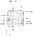
- FIGS. 15 to 17 are enlarged plan views that partially show a top or bottom surface of a second die.
- a base substrate 100 may be formed on a carrier substrate 500 .
- a carrier glue layer 510 may be provided to attach the base substrate 100 to the carrier substrate 500 .
- the base substrate 100 may include an integrated circuit therein.
- the base substrate 100 may be a first die which includes an electronic device such as a transistor.
- the base substrate 100 may be, for example, a wafer-level semiconductor die formed of a semiconductor such as silicon (Si).
- FIG. 11 shows that the base substrate 100 is a first die, but the present inventive concepts are not necessarily limited thereto. According to some embodiments of the present inventive concepts, the base substrate 100 might not include an electronic device such as a transistor. The following will discuss an example in which the base substrate 100 and the first die are the same component.
- the first die 100 may include a signal region SR disposed on a central portion of the first die 100 and a dummy region DR that surrounds the signal region SR.
- the signal region SR may have a first signal region SR 1 and a second signal region SR 2 that are divided from each other.
- the signal region SR may have two second signal regions SR 2 with a first signal region SR 1 disposed therebetween.
- the dummy region DR might not include a wiring line electrically connected to the integrated circuit of the first die 100 .
- the first die 100 may include a first circuit layer 102 and first vias 110 .
- the first circuit layer 102 may be provided on a bottom surface of the first die 100 .
- the first circuit layer 102 may include the integrated circuit.
- the bottom surface of the first die 100 may be an active surface of the first die 100 .
- the first vias 110 may penetrate through the first die 100 in the third direction D 3 .
- the first vias 110 may be electrically connected to the first circuit layer 102 .
- the first vias 110 may include first signal vias 112 provided in the first signal region SR 1 and first power/ground vias 114 provided in the second signal region SR 2 .
- the first die 100 might not include a separate via on the dummy region DR.
- the first die 100 may include first upper pads 120 disposed on the top surface of the first die 100 .
- the first upper pads 120 may include first upper signal pads 122 provided in the signal region SR and first upper dummy pads 124 provided in the dummy region DR.
- the first upper signal pads 122 may be correspondingly coupled to the first vias 110 .
- the first upper signal pads 122 may each have a circular shape when viewed in a plan view.
- An arrangement of the first upper signal pads 122 may conform to the arrangement of the first vias 110 .
- the first upper signal pads 122 may be arranged along the first direction D 1 and the second direction D 2 .
- the first upper dummy pads 124 may be provided in the dummy region DR and may be electrically insulated from the first vias 110 and the first circuit layer 102 .
- the first upper dummy pads 124 may each have a tetragonal shape when viewed in a plan view. For example, some lateral surfaces of the first upper dummy pads 124 may be directed toward the signal region SR, and other lateral surfaces of the first upper dummy pads 124 may be directed toward lateral surfaces of the first die 100 .
- the first upper dummy pads 124 may be arranged in a direction that leads away from the signal region SR. For example, the first upper dummy pads 124 may be arranged along a direction that leads from the signal region SR toward the lateral surfaces of the first die 100 .
- the first die 100 may include external terminals 104 .
- the external terminals 104 may be provided on the bottom surface of the first die 100 .
- the external terminals 104 may be disposed below the first vias 110 .
- the external terminals 104 may be electrically connected to the first circuit layer 102 and the first vias 110 .
- a second die 200 may be provided.
- the second die 200 may include an electronic device such as a transistor.
- the second die 200 may be a wafer-level semiconductor die that includes a semiconductor material such as silicon (Si).
- the second die 200 may have a width less than that of the first die 100 .
- the second die 200 may include a signal region SR that rests on a central portion of the second die 200 and a dummy region DR that surrounds the signal region SR.
- the signal and dummy regions SR and DR of the second die 200 may correspond to the signal and dummy regions SR and DR of the first die 100 .
- the second die 200 may include a second circuit layer 202 and second vias 210 .
- the second circuit layer 202 may be provided on a bottom surface 200 b of the second die 200 .
- the second circuit layer 202 may include an integrated circuit.
- the bottom surface 200 b of the second die 200 may be an active surface of the second die 200 .
- the second vias 210 may penetrate in the third direction D 3 through the second die 200 .
- the second vias 210 may be electrically connected to the second circuit layer 202 .
- the second vias 210 may include second signal vias 212 provided on the first signal region SR 1 and second power/ground vias 214 provided on the second signal region SR 2 .
- the second die 200 may include second upper pads 220 disposed on a top surface 200 a of the second die 200 .
- the second upper pads 220 may include second upper signal pads 222 provided in the signal region SR and second upper dummy pads 224 provided in the dummy region DR.
- the second upper signal pads 222 may be correspondingly coupled to the second vias 210 .
- the second upper signal pads 222 may each have a circular shape when viewed in a plan view.
- An arrangement of the second upper signal pads 222 may conform to the arrangement of the second vias 210 .
- the second upper signal pads 222 may be arranged along the first direction D 1 and the second direction D 2 .
- the second upper dummy pads 224 may be provided in the dummy region DR and may be electrically insulated from the second vias 210 and the second circuit layer 202 .
- the second upper dummy pads 224 may each have a tetragonal shape when viewed in a plan view. For example, some lateral surfaces of the second upper dummy pads 224 may be directed toward the signal region SR, and other lateral surfaces of the second upper dummy pads 224 may be directed toward lateral surfaces SS of the second die 200 .
- the second upper dummy pads 224 may be arranged in a direction that leads away from the signal region SR. For example, the second upper dummy pads 224 may be arranged along a direction that leads from the signal region SR toward the lateral surfaces SS of the second die 200 .
- the second die 200 may include second lower pads 230 disposed on the bottom surface 200 b of the second die 200 .
- the second lower pads 230 may include second lower signal pads 232 provided in the signal region SR and second lower dummy pads 234 provided in the dummy region DR.
- the second lower signal pads 232 may be coupled to the second circuit layer 202 or the second vias 210 .
- the second lower signal pads 232 may each have a circular shape when viewed in a plan view.
- the second lower signal pads 232 may be arranged along the first direction D 1 and the second direction D 2 .
- the second lower dummy pads 234 may be provided in the dummy region DR and may be electrically insulated from the second vias 210 and the second circuit layer 202 .
- the second lower dummy pads 234 may each have a tetragonal shape when viewed in a plan view. For example, some lateral surfaces of the second lower dummy pads 234 may be directed toward the signal region SR, and other lateral surfaces of the second lower dummy pads 234 may be directed toward the lateral surfaces SS of the second die 200 .
- the second lower dummy pads 234 may be arranged in a direction that leads away from the signal region SR. For example, the second lower dummy pads 234 may be arranged along a direction that leads from the signal region SR toward the lateral surfaces SS of the second die 200 .
- the second die 200 may include bumps 240 .
- the bumps 240 may be provided on the bottom surface 200 b of the second die 200 .
- the bumps 240 may be disposed below the second lower pads 230 .
- the bumps 240 may include micro-bumps.
- the bumps 240 may include first bumps 242 disposed below the second lower signal pads 232 and second bumps 244 disposed below the second lower dummy pads 234 .
- the first bumps 242 may be electrically connected to the second circuit layer 202 and the second vias 210 .
- the second bumps 244 may be provided in the dummy region DR and may serve as dummy bumps. In this case, the second bumps 244 may be electrically insulated from the second vias 210 .
- the second bumps 244 may serve to support an outer portion of the second die 200 on the first die 100 , to attach the second die 200 to the first die 100 , and to outwardly transfer heat generated from the first die 100 and the second die 200 .
- An under-fill 300 may be provided below the second die 200 .
- an under-fill material may be coated on the bottom surface 200 b of the second die 200 .
- the under-fill material may surround the bumps 240 .
- a second die 200 may be mounted on the first die 100 .
- the second die 200 and the first die 100 may constitute a chip-on-wafer (COW) structure.
- COW chip-on-wafer
- the second die 200 which has a bottom surface 200 b and the bumps 240 attached thereto, may face down to allow the bottom surface 200 b to face the top surface of the first die 100 .
- the second die 200 may be aligned with the first die 100 so as to place the bumps 240 between the first upper pads 120 and the second lower pads 230 .
- a reflow process may be performed on the bumps 240 . Therefore, the bumps 240 may connect the first upper pads 120 to the second lower pads 230 .
- the first bumps 242 may connect the first upper signal pads 122 to the second lower signal pads 232
- the second bumps 244 may connect the first upper dummy pads 124 to the second lower dummy pads 234 .
- Heat and pressure provided in the reflow process may cause the under-fill 300 to flow between the first die 100 and the second die 200 .
- the under-fill 300 may flow outwardly from a central portion of the second die 200 .
- the under-fill 300 may fill spaces between the first die 100 and the second die 200 .
- a plurality of second dies 200 may be stacked on the second die 200 .
- An uppermost second die 200 might not include a second via 210 .
- a process for mounting the second dies 200 may be substantially the same as the process for mounting the second die 200 on the first die 100 .
- Other second dies 200 may be mounted on one second die 200 .
- the bumps 240 may be attached to the bottom surface 200 b of an overlying second die 200 , and the overlying second die 200 may face down to allow its bottom surface 200 b to face the top surface 200 a of an underlying second die 200 .
- the second dies 200 may be aligned with each other to place the bumps 240 between the second upper pads 220 and the second lower pads 230 .
- a reflow process may be performed on the bumps 240 . Therefore, the bumps 240 may connect the second upper pads 220 to the second lower pads 230 .
- the first bumps 242 may connect the second upper signal pads 222 to the second lower signal pads 232
- the second bumps 244 may connect the second upper dummy pads 224 to the second lower dummy pads 234 .
- melted bumps 240 may be adhered to the second upper pads 220 and the second lower pads 230 .
- surface tension may force the bumps 240 to have their planar shapes conform to those of corresponding second upper pads 220 and those of corresponding second lower pads 230 .
- the first bumps 242 may be formed to have their circular shapes
- the second bumps 244 may be formed to have their tetragonal shapes.
- Heat and pressure provided in the reflow process may cause the under-fill 300 to flow between the first die 100 and the second die 200 .
- the under-fill 300 may flow outwardly from a central portion of the second die 200 .
- the under-fill 300 may flow from the signal region SR positioned on the central portion of the second die 200 toward the lateral surfaces SS of the second die 200 .
- a flow path for the under-fill 300 may have a straight shape between the bumps 240 and the dummy pads 224 and 234 , and the under-fill 300 may flow favorably.
- the under-fill 300 may flow favorably, and thus it may be possible to decrease the occurrence of process defects and to increase structural stability of semiconductor packages.
- the under-fill 300 may fill spaces between the first die 100 and the second die 200 .
- the second upper dummy pads 224 may include third upper dummy pads 226 in first dummy regions DR 1 and fourth upper dummy pads 228 in second dummy regions DR 2 .
- the second lower dummy pads 234 may include third lower dummy pads 236 in the first dummy regions DR 1 and fourth lower dummy pads 238 in the second dummy regions DR 2 .
- the fourth upper dummy pads 228 and the fourth lower dummy pads 238 may have lateral surfaces that are directed toward corners ED of the second die 200 .
- Heat and pressure provided in the reflow process may cause the under-fill 300 to flow between the first die 100 and the second die 200 .
- the under-fill 300 may flow outwardly from a central portion of the second die 200 .
- the under-fill 300 may flow from the signal region SR toward the lateral surface SS of the second die 200
- the second dummy region DR 2 adjacent to the corner (see ED of FIG. 6 ) of the second die 200 the under-fill 300 may flow from the signal region SR toward the corner ED of the second die 200 .
- the dummy pads 224 and 234 and the bumps 240 may be aligned such that their lateral surfaces face the corner ED of the second die 200 , and the under-fill 300 may flow favorably.
- the second upper dummy pads 224 may include third upper dummy pads 226 in first dummy regions DR 1 and fourth upper dummy pads 228 in second dummy regions DR 2 .
- the second lower dummy pads 234 may include third lower dummy pads 236 in the first dummy regions DR 1 and fourth lower dummy pads 238 in the second dummy regions DR 2 .
- the fourth upper dummy pads 228 and the fourth lower dummy pads 238 may be arranged in radial direction(s) that lead from the signal region SR.
- Heat and pressure provided in the reflow process may cause the under-fill 300 to flow between the first die 100 and the second die 200 .
- the under-fill 300 may flow outwardly from a central portion of the second die 200 .
- the under-fill 300 may flow from the signal region SR toward the lateral surface SS of the second die 200 , and in the second dummy region DR 2 adjacent to the corner (see ED of FIG. 8 ) of the second die 200 , the under-fill 300 may flow divergently in direction(s) from the signal region SR.
- the dummy pads 224 and 234 and the bumps 240 may be arranged radially, and the under-fill 300 may flow more favorably.
- the plurality of second dies 200 may be electrically connected to each other through the bumps 240 provided on the bottom surfaces 200 b thereof.
- the bumps 240 may connect the second upper pads 220 to the second lower pads 230 that are adjacent in the third direction D 3 to the second upper pads 220 .
- a molding layer 400 may be formed on the top surface of the first die 100 .
- the molding layer 400 may cover the top surface of the first die 100 .
- the molding layer 400 may surround the second dies 200 .
- the molding layer 400 may include a dielectric polymer material.
- the molding layer 400 may include an epoxy molding compound (EMC).
- the carrier substrate 500 and the carrier glue layer 510 may be removed.
- the carrier substrate 500 and the carrier glue layer 510 may be removed to expose the external terminals 104 and a passivation layer of the first die 100 .
- a semiconductor package according to some embodiments of the present inventive concepts may increase thermal radiation efficiency of dies therein without causing an under-fill to have a reduced width between the dies.
- the under-fill may not be obstructed during a flow process in a fabrication process of the semiconductor package.
- an under-fill may have a straight flow path between dummy pads and bumps, and the under-fill may flow favorably, and accordingly process defects may be prevented.
Landscapes
- Engineering & Computer Science (AREA)
- Microelectronics & Electronic Packaging (AREA)
- Power Engineering (AREA)
- Computer Hardware Design (AREA)
- Physics & Mathematics (AREA)
- Condensed Matter Physics & Semiconductors (AREA)
- General Physics & Mathematics (AREA)
- Semiconductor Integrated Circuits (AREA)
- Control And Other Processes For Unpacking Of Materials (AREA)
- Internal Circuitry In Semiconductor Integrated Circuit Devices (AREA)
Abstract
Description
Claims (17)
Priority Applications (1)
| Application Number | Priority Date | Filing Date | Title |
|---|---|---|---|
| US18/826,592 US20240429205A1 (en) | 2021-03-11 | 2024-09-06 | Semiconductor package with increased thermal radiation efficiency |
Applications Claiming Priority (2)
| Application Number | Priority Date | Filing Date | Title |
|---|---|---|---|
| KR1020210032273A KR102900182B1 (en) | 2021-03-11 | 2021-03-11 | Semiconductor package |
| KR10-2021-0032273 | 2021-03-11 |
Related Child Applications (1)
| Application Number | Title | Priority Date | Filing Date |
|---|---|---|---|
| US18/826,592 Continuation US20240429205A1 (en) | 2021-03-11 | 2024-09-06 | Semiconductor package with increased thermal radiation efficiency |
Publications (2)
| Publication Number | Publication Date |
|---|---|
| US20220293566A1 US20220293566A1 (en) | 2022-09-15 |
| US12113050B2 true US12113050B2 (en) | 2024-10-08 |
Family
ID=83195060
Family Applications (2)
| Application Number | Title | Priority Date | Filing Date |
|---|---|---|---|
| US17/552,614 Active 2042-09-02 US12113050B2 (en) | 2021-03-11 | 2021-12-16 | Semiconductor package with increased thermal radiation efficiency |
| US18/826,592 Pending US20240429205A1 (en) | 2021-03-11 | 2024-09-06 | Semiconductor package with increased thermal radiation efficiency |
Family Applications After (1)
| Application Number | Title | Priority Date | Filing Date |
|---|---|---|---|
| US18/826,592 Pending US20240429205A1 (en) | 2021-03-11 | 2024-09-06 | Semiconductor package with increased thermal radiation efficiency |
Country Status (2)
| Country | Link |
|---|---|
| US (2) | US12113050B2 (en) |
| KR (1) | KR102900182B1 (en) |
Families Citing this family (3)
| Publication number | Priority date | Publication date | Assignee | Title |
|---|---|---|---|---|
| KR20220169043A (en) * | 2021-06-17 | 2022-12-27 | 삼성전자주식회사 | Semiconductor package and method of fabricating the same |
| KR20240108934A (en) * | 2023-01-02 | 2024-07-10 | 삼성전자주식회사 | Semiconductor and method of manufacturing the same |
| US20250105083A1 (en) * | 2023-09-27 | 2025-03-27 | Analog Power Conversion LLC | Electronic module configured for thermal management |
Citations (14)
| Publication number | Priority date | Publication date | Assignee | Title |
|---|---|---|---|---|
| JP3416040B2 (en) | 1997-11-11 | 2003-06-16 | 富士通株式会社 | Semiconductor device |
| JP2009218233A (en) | 2008-03-06 | 2009-09-24 | Nec Corp | Semiconductor device and method of manufacturing the same |
| US20120098120A1 (en) | 2010-10-21 | 2012-04-26 | Taiwan Semiconductor Manufacturing Company, Ltd. | Centripetal layout for low stress chip package |
| US8283781B2 (en) | 2010-09-10 | 2012-10-09 | Taiwan Semiconductor Manufacturing Company, Ltd. | Semiconductor device having pad structure with stress buffer layer |
| US20160013144A1 (en) * | 2014-06-12 | 2016-01-14 | Taiwan Semiconductor Manufacturing Company, Ltd. | Pad Design For Reliability Enhancement in Packages |
| US20160079208A1 (en) * | 2014-09-11 | 2016-03-17 | Junyeong HEO | Semiconductor package and method of fabricating the same |
| US9559071B2 (en) | 2013-06-26 | 2017-01-31 | Taiwan Semiconductor Manufacturing Company, Ltd. | Mechanisms for forming hybrid bonding structures with elongated bumps |
| US9564412B2 (en) | 2011-12-06 | 2017-02-07 | Intel Corporation | Shaped and oriented solder joints |
| US9589921B2 (en) | 2013-03-13 | 2017-03-07 | Ps4 Luxco S.A.R.L. | Semiconductor device |
| US20190363068A1 (en) | 2017-03-21 | 2019-11-28 | Fujifilm Corporation | Stacked device, stacked structure, and method of manufacturing stacked device |
| US10546844B2 (en) | 2015-11-26 | 2020-01-28 | Samsung Electronics Co., Ltd. | Stack package and method of manufacturing the stack package |
| US20200091075A1 (en) | 2014-01-16 | 2020-03-19 | Taiwan Semiconductor Manufacturing Company, Ltd. | Pad Structure Design in Fan-Out Package |
| US10784219B2 (en) | 2017-11-30 | 2020-09-22 | Taiwan Semiconductor Manufacturing Company, Ltd. | Semiconductor device and method of manufacturing |
| US20210305184A1 (en) * | 2020-03-26 | 2021-09-30 | Beijing Xiaomi Mobile Software Co., Ltd. | Chip, circuit board and electronic device |
-
2021
- 2021-03-11 KR KR1020210032273A patent/KR102900182B1/en active Active
- 2021-12-16 US US17/552,614 patent/US12113050B2/en active Active
-
2024
- 2024-09-06 US US18/826,592 patent/US20240429205A1/en active Pending
Patent Citations (14)
| Publication number | Priority date | Publication date | Assignee | Title |
|---|---|---|---|---|
| JP3416040B2 (en) | 1997-11-11 | 2003-06-16 | 富士通株式会社 | Semiconductor device |
| JP2009218233A (en) | 2008-03-06 | 2009-09-24 | Nec Corp | Semiconductor device and method of manufacturing the same |
| US8283781B2 (en) | 2010-09-10 | 2012-10-09 | Taiwan Semiconductor Manufacturing Company, Ltd. | Semiconductor device having pad structure with stress buffer layer |
| US20120098120A1 (en) | 2010-10-21 | 2012-04-26 | Taiwan Semiconductor Manufacturing Company, Ltd. | Centripetal layout for low stress chip package |
| US9564412B2 (en) | 2011-12-06 | 2017-02-07 | Intel Corporation | Shaped and oriented solder joints |
| US9589921B2 (en) | 2013-03-13 | 2017-03-07 | Ps4 Luxco S.A.R.L. | Semiconductor device |
| US9559071B2 (en) | 2013-06-26 | 2017-01-31 | Taiwan Semiconductor Manufacturing Company, Ltd. | Mechanisms for forming hybrid bonding structures with elongated bumps |
| US20200091075A1 (en) | 2014-01-16 | 2020-03-19 | Taiwan Semiconductor Manufacturing Company, Ltd. | Pad Structure Design in Fan-Out Package |
| US20160013144A1 (en) * | 2014-06-12 | 2016-01-14 | Taiwan Semiconductor Manufacturing Company, Ltd. | Pad Design For Reliability Enhancement in Packages |
| US20160079208A1 (en) * | 2014-09-11 | 2016-03-17 | Junyeong HEO | Semiconductor package and method of fabricating the same |
| US10546844B2 (en) | 2015-11-26 | 2020-01-28 | Samsung Electronics Co., Ltd. | Stack package and method of manufacturing the stack package |
| US20190363068A1 (en) | 2017-03-21 | 2019-11-28 | Fujifilm Corporation | Stacked device, stacked structure, and method of manufacturing stacked device |
| US10784219B2 (en) | 2017-11-30 | 2020-09-22 | Taiwan Semiconductor Manufacturing Company, Ltd. | Semiconductor device and method of manufacturing |
| US20210305184A1 (en) * | 2020-03-26 | 2021-09-30 | Beijing Xiaomi Mobile Software Co., Ltd. | Chip, circuit board and electronic device |
Also Published As
| Publication number | Publication date |
|---|---|
| US20220293566A1 (en) | 2022-09-15 |
| KR20220127671A (en) | 2022-09-20 |
| US20240429205A1 (en) | 2024-12-26 |
| KR102900182B1 (en) | 2025-12-15 |
Similar Documents
| Publication | Publication Date | Title |
|---|---|---|
| US10784244B2 (en) | Semiconductor package including multiple semiconductor chips and method of manufacturing the semiconductor package | |
| US20240429205A1 (en) | Semiconductor package with increased thermal radiation efficiency | |
| US7402911B2 (en) | Multi-chip device and method for producing a multi-chip device | |
| KR101736984B1 (en) | Print circuit board having hexagonal bump pad for substrate of semiconductor package and semiconductor package having the same | |
| US12237302B2 (en) | Semiconductor package | |
| US11862570B2 (en) | Semiconductor package | |
| KR102517464B1 (en) | Semiconductor package include bridge die spaced apart semiconductor die | |
| JP2009044110A (en) | Semiconductor device and manufacturing method thereof | |
| US6072700A (en) | Ball grid array package | |
| TW201737446A (en) | Semiconductor package with multiple coplanar interposers | |
| US20240371835A1 (en) | Semiconductor package and method of fabricating the same | |
| US20220149010A1 (en) | Semiconductor packages | |
| US20240063129A1 (en) | Semiconductor package | |
| US12368136B2 (en) | Semiconductor package and a method of manufacturing the semiconductor package | |
| CN118352323A (en) | Semiconductor package | |
| US20250192094A1 (en) | Semiconductor package | |
| TWI911402B (en) | Semiconductor package | |
| US20240404970A1 (en) | Semiconductor package | |
| US20250006720A1 (en) | Semiconductor package and method of manufacturing the semiconductor package | |
| US20260018475A1 (en) | Semiconductor package | |
| TWI841184B (en) | Semiconductor package and manufacturing method thereof | |
| US20240379481A1 (en) | Semiconductor package including a plurality of chips sequentially stacked on a package substrate by an adhesive film and method of manufacturing the semiconductor package | |
| KR20240137931A (en) | Semiconductor package and method of fabricating of the same | |
| KR20230068244A (en) | Redistribution substrate, and semiconductor package including the same | |
| KR20260013007A (en) | Semiconductor package |
Legal Events
| Date | Code | Title | Description |
|---|---|---|---|
| AS | Assignment |
Owner name: SAMSUNG ELECTRONICS CO., LTD., KOREA, REPUBLIC OF Free format text: ASSIGNMENT OF ASSIGNORS INTEREST;ASSIGNORS:PARK, SANG-SICK;KANG, UN-BYOUNG;LEE, JONGHO;AND OTHERS;REEL/FRAME:058522/0456 Effective date: 20211130 |
|
| FEPP | Fee payment procedure |
Free format text: ENTITY STATUS SET TO UNDISCOUNTED (ORIGINAL EVENT CODE: BIG.); ENTITY STATUS OF PATENT OWNER: LARGE ENTITY |
|
| STPP | Information on status: patent application and granting procedure in general |
Free format text: DOCKETED NEW CASE - READY FOR EXAMINATION |
|
| STPP | Information on status: patent application and granting procedure in general |
Free format text: NON FINAL ACTION MAILED |
|
| STPP | Information on status: patent application and granting procedure in general |
Free format text: RESPONSE TO NON-FINAL OFFICE ACTION ENTERED AND FORWARDED TO EXAMINER |
|
| STPP | Information on status: patent application and granting procedure in general |
Free format text: FINAL REJECTION MAILED |
|
| STPP | Information on status: patent application and granting procedure in general |
Free format text: RESPONSE AFTER FINAL ACTION FORWARDED TO EXAMINER |
|
| STPP | Information on status: patent application and granting procedure in general |
Free format text: NOTICE OF ALLOWANCE MAILED -- APPLICATION RECEIVED IN OFFICE OF PUBLICATIONS |
|
| ZAAA | Notice of allowance and fees due |
Free format text: ORIGINAL CODE: NOA |
|
| ZAAB | Notice of allowance mailed |
Free format text: ORIGINAL CODE: MN/=. |
|
| STPP | Information on status: patent application and granting procedure in general |
Free format text: PUBLICATIONS -- ISSUE FEE PAYMENT VERIFIED |
|
| STCF | Information on status: patent grant |
Free format text: PATENTED CASE |