US12111427B2 - Ultrasonic detection device - Google Patents
Ultrasonic detection device Download PDFInfo
- Publication number
- US12111427B2 US12111427B2 US17/406,119 US202117406119A US12111427B2 US 12111427 B2 US12111427 B2 US 12111427B2 US 202117406119 A US202117406119 A US 202117406119A US 12111427 B2 US12111427 B2 US 12111427B2
- Authority
- US
- United States
- Prior art keywords
- elements
- test
- dummy
- sensing
- detection device
- Prior art date
- Legal status (The legal status is an assumption and is not a legal conclusion. Google has not performed a legal analysis and makes no representation as to the accuracy of the status listed.)
- Active, expires
Links
Images


Classifications
-
- G—PHYSICS
- G01—MEASURING; TESTING
- G01S—RADIO DIRECTION-FINDING; RADIO NAVIGATION; DETERMINING DISTANCE OR VELOCITY BY USE OF RADIO WAVES; LOCATING OR PRESENCE-DETECTING BY USE OF THE REFLECTION OR RERADIATION OF RADIO WAVES; ANALOGOUS ARRANGEMENTS USING OTHER WAVES
- G01S15/00—Systems using the reflection or reradiation of acoustic waves, e.g. sonar systems
- G01S15/88—Sonar systems specially adapted for specific applications
- G01S15/89—Sonar systems specially adapted for specific applications for mapping or imaging
-
- A—HUMAN NECESSITIES
- A61—MEDICAL OR VETERINARY SCIENCE; HYGIENE
- A61B—DIAGNOSIS; SURGERY; IDENTIFICATION
- A61B8/00—Diagnosis using ultrasonic, sonic or infrasonic waves
- A61B8/44—Constructional features of the ultrasonic, sonic or infrasonic diagnostic device
-
- B—PERFORMING OPERATIONS; TRANSPORTING
- B06—GENERATING OR TRANSMITTING MECHANICAL VIBRATIONS IN GENERAL
- B06B—METHODS OR APPARATUS FOR GENERATING OR TRANSMITTING MECHANICAL VIBRATIONS OF INFRASONIC, SONIC, OR ULTRASONIC FREQUENCY, e.g. FOR PERFORMING MECHANICAL WORK IN GENERAL
- B06B1/00—Methods or apparatus for generating mechanical vibrations of infrasonic, sonic, or ultrasonic frequency
- B06B1/02—Methods or apparatus for generating mechanical vibrations of infrasonic, sonic, or ultrasonic frequency making use of electrical energy
- B06B1/0292—Electrostatic transducers, e.g. electret-type
-
- G—PHYSICS
- G01—MEASURING; TESTING
- G01S—RADIO DIRECTION-FINDING; RADIO NAVIGATION; DETERMINING DISTANCE OR VELOCITY BY USE OF RADIO WAVES; LOCATING OR PRESENCE-DETECTING BY USE OF THE REFLECTION OR RERADIATION OF RADIO WAVES; ANALOGOUS ARRANGEMENTS USING OTHER WAVES
- G01S15/00—Systems using the reflection or reradiation of acoustic waves, e.g. sonar systems
- G01S15/02—Systems using the reflection or reradiation of acoustic waves, e.g. sonar systems using reflection of acoustic waves
-
- G—PHYSICS
- G01—MEASURING; TESTING
- G01S—RADIO DIRECTION-FINDING; RADIO NAVIGATION; DETERMINING DISTANCE OR VELOCITY BY USE OF RADIO WAVES; LOCATING OR PRESENCE-DETECTING BY USE OF THE REFLECTION OR RERADIATION OF RADIO WAVES; ANALOGOUS ARRANGEMENTS USING OTHER WAVES
- G01S15/00—Systems using the reflection or reradiation of acoustic waves, e.g. sonar systems
- G01S15/88—Sonar systems specially adapted for specific applications
- G01S15/89—Sonar systems specially adapted for specific applications for mapping or imaging
- G01S15/8906—Short-range imaging systems; Acoustic microscope systems using pulse-echo techniques
- G01S15/8909—Short-range imaging systems; Acoustic microscope systems using pulse-echo techniques using a static transducer configuration
- G01S15/8915—Short-range imaging systems; Acoustic microscope systems using pulse-echo techniques using a static transducer configuration using a transducer array
- G01S15/8925—Short-range imaging systems; Acoustic microscope systems using pulse-echo techniques using a static transducer configuration using a transducer array the array being a two-dimensional transducer configuration, i.e. matrix or orthogonal linear arrays
-
- G—PHYSICS
- G01—MEASURING; TESTING
- G01S—RADIO DIRECTION-FINDING; RADIO NAVIGATION; DETERMINING DISTANCE OR VELOCITY BY USE OF RADIO WAVES; LOCATING OR PRESENCE-DETECTING BY USE OF THE REFLECTION OR RERADIATION OF RADIO WAVES; ANALOGOUS ARRANGEMENTS USING OTHER WAVES
- G01S15/00—Systems using the reflection or reradiation of acoustic waves, e.g. sonar systems
- G01S15/88—Sonar systems specially adapted for specific applications
- G01S15/89—Sonar systems specially adapted for specific applications for mapping or imaging
- G01S15/8906—Short-range imaging systems; Acoustic microscope systems using pulse-echo techniques
- G01S15/8909—Short-range imaging systems; Acoustic microscope systems using pulse-echo techniques using a static transducer configuration
- G01S15/8915—Short-range imaging systems; Acoustic microscope systems using pulse-echo techniques using a static transducer configuration using a transducer array
- G01S15/8927—Short-range imaging systems; Acoustic microscope systems using pulse-echo techniques using a static transducer configuration using a transducer array using simultaneously or sequentially two or more subarrays or subapertures
-
- G—PHYSICS
- G01—MEASURING; TESTING
- G01S—RADIO DIRECTION-FINDING; RADIO NAVIGATION; DETERMINING DISTANCE OR VELOCITY BY USE OF RADIO WAVES; LOCATING OR PRESENCE-DETECTING BY USE OF THE REFLECTION OR RERADIATION OF RADIO WAVES; ANALOGOUS ARRANGEMENTS USING OTHER WAVES
- G01S7/00—Details of systems according to groups G01S13/00, G01S15/00, G01S17/00
- G01S7/52—Details of systems according to groups G01S13/00, G01S15/00, G01S17/00 of systems according to group G01S15/00
- G01S7/52004—Means for monitoring or calibrating
-
- G—PHYSICS
- G01—MEASURING; TESTING
- G01S—RADIO DIRECTION-FINDING; RADIO NAVIGATION; DETERMINING DISTANCE OR VELOCITY BY USE OF RADIO WAVES; LOCATING OR PRESENCE-DETECTING BY USE OF THE REFLECTION OR RERADIATION OF RADIO WAVES; ANALOGOUS ARRANGEMENTS USING OTHER WAVES
- G01S7/00—Details of systems according to groups G01S13/00, G01S15/00, G01S17/00
- G01S7/52—Details of systems according to groups G01S13/00, G01S15/00, G01S17/00 of systems according to group G01S15/00
- G01S7/52017—Details of systems according to groups G01S13/00, G01S15/00, G01S17/00 of systems according to group G01S15/00 particularly adapted to short-range imaging
- G01S7/5205—Means for monitoring or calibrating
-
- G—PHYSICS
- G01—MEASURING; TESTING
- G01S—RADIO DIRECTION-FINDING; RADIO NAVIGATION; DETERMINING DISTANCE OR VELOCITY BY USE OF RADIO WAVES; LOCATING OR PRESENCE-DETECTING BY USE OF THE REFLECTION OR RERADIATION OF RADIO WAVES; ANALOGOUS ARRANGEMENTS USING OTHER WAVES
- G01S7/00—Details of systems according to groups G01S13/00, G01S15/00, G01S17/00
- G01S7/52—Details of systems according to groups G01S13/00, G01S15/00, G01S17/00 of systems according to group G01S15/00
- G01S7/521—Constructional features
Definitions
- the disclosure relates to an ultrasonic detection device, and more particularly to an ultrasonic detection device including a first test element.
- the ultrasonic detection device adopts a technology that obtains images through emitting and receiving ultrasonic waves.
- many apparatuses use ultrasonic detection technology.
- a car or a drone uses an ultrasonic detection device to measure a distance; and a doctor uses an apparatus with an ultrasonic detection device to check the physical condition of a patient.
- common ultrasonic detection devices include a capacitive micromachined ultrasonic transducer (CMUT) and a piezoelectric micromachined ultrasonic transducer (PMUT).
- CMUT capacitive micromachined ultrasonic transducer
- PMUT piezoelectric micromachined ultrasonic transducer
- the CMUT contains two electrodes, and there is an insulating film between the two electrodes. By controlling the voltage of the electrodes, the insulating film vibrates and emits ultrasonic waves.
- the disclosure provides an ultrasonic detection device, which can improve the issue of poor image quality due to the test process of the ultrasonic detection device.
- the ultrasonic detection device includes a substrate, multiple sensing elements, a first test element, a first dummy element, at least one first common signal line, multiple sensing signal lines, and a test signal line.
- the sensing elements, the first test element, and the first dummy element are located on the substrate.
- the first test element is located between the sensing elements and the first dummy element.
- Each of the sensing elements, the first test element, and the first dummy element includes an array of multiple capacitive microelectromechanical ultrasonic transducers.
- the first common signal line is electrically connected to the sensing elements and the first test element.
- the sensing signal lines are electrically connected to the sensing elements.
- the test signal line is electrically connected to the first test element.
- FIG. 1 A is a schematic top view of an ultrasonic detection device according to an embodiment of the disclosure.
- FIG. 1 B is a partial enlarged view of the ultrasonic detection device of FIG. 1 A .
- FIG. 1 C is a partial enlarged view of the ultrasonic detection device of FIG. 1 B .
- FIG. 2 is a schematic cross-sectional view corresponding to lines A-A′, B-B′, and C-C′ in FIG. 1 C .
- FIG. 3 is a schematic top view of an ultrasonic detection device according to an embodiment of the disclosure.
- FIG. 4 is a schematic side view of an ultrasonic detection apparatus according to an embodiment of the disclosure.
- FIG. 5 is a schematic side view of an ultrasonic detection apparatus according to an embodiment of the disclosure.
- FIG. 6 A is a schematic top view of an ultrasonic detection device according to an embodiment of the disclosure.
- FIG. 6 B is a partial enlarged view of the ultrasonic detection device of FIG. 6 A .
- FIG. 7 is a schematic side view of an ultrasonic detection apparatus according to an embodiment of the disclosure.
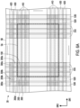
- FIG. 1 A is a schematic top view of an ultrasonic detection device 10 according to an embodiment of the disclosure.
- FIG. 1 B is a partial enlarged view of the ultrasonic detection device 10 of FIG. 1 A , wherein FIG. 1 B corresponds to a position of a region R 1 of FIG. 1 A .
- FIG. 1 C is a partial enlarged view of the ultrasonic detection device 10 of FIG. 1 B , wherein FIG. 1 C corresponds to positions of regions R 2 , R 3 , and R 4 of FIG. 1 B .
- FIG. 2 is a schematic cross-sectional view corresponding to a line A-A′ in FIG. 1 C .
- the ultrasonic detection device 10 includes a substrate SB, multiple sensing elements 100 , one or more first test elements 200 , one or more first dummy elements 300 , a first common signal line 410 , multiple sensing signal lines 510 , and one or more test signal lines 520 .
- the ultrasonic detection device 10 has a sensing area SA, wherein the sensing elements 100 are disposed in the sensing area SA, and the first test elements 200 and the first dummy elements 300 are disposed outside the sensing area SA.
- the ultrasonic detection device 10 further includes an alignment mark M.
- the alignment mark M is disposed on the substrate SB and is suitable for improving the accuracy of various manufacturing processes of the ultrasonic detection device 10 .
- the sensing elements 100 , the first test elements 200 , and the first dummy elements 300 are located on the substrate SB.
- the first test elements 200 are located between the sensing elements 100 and the first dummy elements 300 .
- the sensing elements 100 , the first test elements 200 , and the first dummy elements 300 are arranged in a first direction DR 1 .
- the ultrasonic detection device 10 includes two first test elements 200 and two first dummy elements 300 , the sensing element 100 is located between the two first test elements 200 , and the sensing elements 100 and the first test elements 200 are located between the two first dummy elements 300 .
- the ultrasonic detection device 10 includes 64 to 256 sensing elements 100 .
- Each of the sensing elements 100 , the first test elements 200 , and the first dummy elements 300 includes an array of multiple capacitive microelectromechanical ultrasonic transducers 110 , 210 , and 310 .
- the sensing element 100 includes the capacitive microelectromechanical ultrasonic transducers 110 arranged along the first direction DR 1 and a second direction DR 2
- the first test element 200 includes the capacitive microelectromechanical ultrasonic transducers 210 arranged along the first direction DR 1 and the second direction DR 2
- the first dummy element 300 includes an array of capacitive microelectromechanical ultrasonic transducers 310 arranged along the first direction DR 1 and the second direction DR 2 .
- the first direction DR 1 is substantially perpendicular to the second direction DR 2 .
- the number of capacitive microelectromechanical ultrasonic transducers 110 , 210 , and 310 of each of the sensing elements 100 , the first test elements 200 , and the first dummy elements 300 are the same as one another.
- the arrangement manner and the number of capacitive microelectromechanical ultrasonic transducers 110 in one sensing element 100 are equal to the arrangement manner and the number of capacitive microelectromechanical ultrasonic transducers 210 in one first test element 200
- the arrangement manner and the number of capacitive microelectromechanical ultrasonic transducers 210 in one first test element 200 are equal to the arrangement manner and the number of capacitive microelectromechanical ultrasonic transducers 310 in one first dummy element 300 .
- the sensing element 100 , the first test element 200 , and the first dummy element 300 have structures similar to one another.
- the first common signal line 410 is electrically connected to the capacitive microelectromechanical ultrasonic transducer 110 of the sensing element 100 and the capacitive microelectromechanical ultrasonic transducer 210 of the first test element 200 .
- the first common signal line 410 includes a main portion 412 , multiple first branch portions 414 overlapping with the first test element 200 , and multiple second branch portions 416 overlapping with the sensing element 100 .
- the first branch portions 414 and the second branch portions 416 are connected to one side of the main portion 412 .
- the first branch portions 414 are electrically connected to the first test element 200
- the second branch portions 416 are electrically connected to the sensing element 100 .
- the sensing signal line 510 is electrically connected to the capacitive microelectromechanical ultrasonic transducer 110 of the sensing element 100 .
- the test signal line 520 is electrically connected to the capacitive microelectromechanical ultrasonic transducer 210 of the first test element 200 .
- the sensing signal line 510 and the test signal line 520 may be used as bonding pads for connecting chips (not shown).
- the chips are disposed on the sensing signal line 510 and the test signal line 520 and are electrically connected to the sensing signal line 510 and the test signal line 520 .
- the sensing signal line 510 and the test signal line 520 are electrically connected to the same or different chips.
- the ultrasonic detection device 10 further includes multiple dummy common signal lines 420 and multiple dummy sensing signal lines 530 .
- the dummy common signal line 420 overlaps with the dummy sensing signal line 530 .
- the dummy common signal line 420 and the dummy sensing signal line 530 are electrically connected to the capacitive microelectromechanical ultrasonic transducer 310 of the first dummy element 300 .
- the dummy common signal line 420 , the first branch portion 414 , and the second branch portion 416 are substantially parallel to one another.
- the dummy common signal line 420 , the first branch portion 414 , and the second branch portion 416 are substantially parallel to the second direction DR 2 .
- the capacitive microelectromechanical ultrasonic transducers 110 , 210 , and 310 have similar structures.
- Each of the capacitive microelectromechanical ultrasonic transducers 110 , 210 , and 310 includes a first electrode and a second electrode separated from the first electrode.
- a first electrode 112 of the capacitive microelectromechanical ultrasonic transducer 110 of the sensing element 100 , a first electrode 212 of the capacitive microelectromechanical ultrasonic transducer 210 of the first test element 200 , a first electrode 312 of the capacitive microelectromechanical ultrasonic transducer 310 of the first dummy element 300 , the first common signal line 410 , and the dummy common signal line 420 are disposed on the substrate SB.
- the first electrode 112 , the first electrode 212 , and the first electrode 312 are connected to the first common signal line 410 , and the first electrode 312 is connected to the dummy common signal line 420 .
- the chips or other driving circuits are electrically connected to the first common signal line 410 and provide voltage to the first common signal line 410 .
- the dummy common signal line 420 does not directly receive signals provided by the chips or other driving circuits. Therefore, the first electrode 312 is a floating electrode.
- the first electrode 112 , the first electrode 212 , the first electrode 312 , the first common signal line 410 , and the dummy common signal line 420 belong to the same conductive film layer.
- the first electrode 112 , the first electrode 212 , the first electrode 312 , the first common signal line 410 , and the dummy common signal line 420 are formed by patterning the same layer of conductive material.
- the first electrode 112 , the first electrode 212 , the first electrode 312 , the first common signal line 410 , and the dummy common signal line 420 have a single-layer or multi-layer (for example, a titanium layer, an aluminum layer, and a stacked layer of titanium layers) structure, and the materials of the first electrode 112 , the first electrode 212 , the first electrode 312 , the first common signal line 410 , and the dummy common signal line 420 include metals, nitrides of metallic materials, oxides of metallic materials, oxynitrides of metallic materials, other suitable materials, or stacked layers of metallic materials and other conductive materials.
- the first electrode 112 of the capacitive microelectromechanical ultrasonic transducer 110 of the sensing element 100 , the first electrode 212 of the capacitive microelectromechanical ultrasonic transducer 210 of the first test element 200 , and the first common signal line 410 are connected as one.
- the first electrode 312 of the capacitive microelectromechanical ultrasonic transducer 310 of the first dummy element 300 and the dummy common signal line 420 are connected as one.
- An insulating layer IL is located on the first electrodes 112 , 212 , and 312 , the first common signal line 410 , and the dummy common signal line 420 .
- the insulating layer IL has multiple grooves C, and each groove C overlaps with multiple corresponding capacitive microelectromechanical ultrasonic transducers 110 , 210 , and 310 .
- the grooves C extend along the first direction DR 1 .
- a part of the insulating layer IL is located on top of the grooves C and constitutes a thin film F. Multiple through holes TH pass through the thin film F.
- a filling material FL is located on the insulating layer IL and is filled into the through holes TH, thereby sealing the grooves C.
- the filling material FL includes, for example, cured photoresist, silicon-containing nitride, silicon-containing oxide, or other insulating materials.
- a second electrode 114 of the capacitive microelectromechanical ultrasonic transducer 110 of the sensing element 100 , a second electrode 214 of the capacitive microelectromechanical ultrasonic transducer 210 of the first test element 200 , a second electrode 314 of the capacitive microelectromechanical ultrasonic transducer 310 of the first dummy element 300 , the sensing signal line 510 , the test signal line 520 , and the dummy sensing signal line 530 are disposed on the insulating layer IL.
- the second electrode 114 is electrically connected to the sensing signal line 510
- the second electrode 214 is electrically connected to the test signal line 520
- the second electrode 314 is connected to the dummy sensing signal line 530 .
- the chips or other driving circuits (not shown) are electrically connected to the sensing signal line 510 and the test signal line 520 , and provide voltage to the sensing signal line 510 and the test signal line 520 .
- the dummy sensing signal line 530 does not directly receive signals provided by the chips or other driving circuits. Therefore, the second electrode 314 is a floating electrode.
- the second electrode 114 , the second electrode 214 , the second electrode 314 , the sensing signal line 510 , the test signal line 520 , and the dummy sensing signal line 530 belong to the same conductive film layer.
- the second electrode 114 , the second electrode 214 , the second electrode 314 , the sensing signal line 510 , the test signal line 520 , and the dummy sensing signal line 530 are formed by patterning the same layer of conductive material.
- the second electrode 114 , the second electrode 214 , the second electrode 314 , the sensing signal line 510 , the test signal line 520 , and the dummy sensing signal line 530 have a single-layer or multi-layer (such as a molybdenum layer, an aluminum layer, and a stacked layer of molybdenum layers) structure, and the materials of the second electrode 114 , the second electrode 214 , the second electrode 314 , the sensing signal line 510 , the test signal line 520 , and the dummy sensing signal line 530 include metals, nitrides of metallic materials, oxides of metallic materials, oxynitrides of metallic materials, other suitable materials, or stacked layers of metallic materials and other conductive materials.
- the second electrodes 114 of the capacitive microelectromechanical ultrasonic transducer 110 of the sensing element 100 are respectively connected as one with the corresponding sensing signal lines 510
- the second electrodes 214 of the capacitive microelectromechanical ultrasonic transducer 210 of the first test element 200 are respectively connected as one with the corresponding test signal lines 520
- the second electrodes 314 of the capacitive microelectromechanical ultrasonic transducer 310 of the first dummy element 300 are respectively connected as one with the corresponding dummy sensing signal lines 530 .
- the ultrasonic detection device 10 further includes a shock-absorbing material SM.
- the shock-absorbing material SM is disposed on a back surface of the substrate SB, and the sensing element 100 , the first test element 200 and the first dummy element 300 are disposed on a front surface of the substrate SB.
- the first test element 200 is suitable for testing the breakdown voltage of the ultrasonic detection device 10 .
- a test process is executed on the ultrasonic detection device 10 , wherein the test process is, for example, an impedance test or an acoustic test.
- the test process is, for example, an impedance test or an acoustic test.
- voltage is repeatedly applied to the first test element 200 until the first test element 200 collapses.
- the sensing elements 100 in the sensing area SA affect one another.
- the performance of each sensing element 100 is affected by the adjacent sensing element 100 or the first test element 200 . Therefore, in order for the first test element 200 to have the performance similar to the sensing elements 100 , the first dummy element 300 is disposed such that the first test element 200 is located between the first dummy element 300 and the sensing elements 100 . In other words, by the configuration of the first dummy element 300 , the performance of the first test element 200 may be closer to the performance of the sensing elements 100 in the sensing area SA, thereby improving the reliability of the test process.
- a part or all of the capacitive microelectromechanical ultrasonic transducers 210 in the first test element 200 collapse after repeatedly applying voltage. Since the first test element 200 is disposed outside the sensing area SA, even if the first test element 200 collapses, an image generated by the sensing elements 100 in the sensing area SA will not be greatly affected. In other words, the quality of the image displayed by the ultrasonic detection device 10 may be maintained by sacrificing the first test element 200 .
- a pitch P 1 between the first test element 200 and the adjacent sensing element 100 is approximately equal to a pitch P 2 between the first test element 200 and the first dummy element 300
- the pitch P 1 between the first test element 200 and the adjacent sensing element 100 is equal to a pitch P 3 between two adjacent sensing elements 100 .
- the pitch P 1 , the pitch P 2 , and the pitch P 3 are, for example, 0.1 mm to 1 mm.
- a width W 1 of the sensing element 100 , a width W 2 of the first test element 200 , and a width W 3 of the first dummy element 300 are the same as one another.
- a center frequency of an ultrasonic wave emitted by the ultrasonic detection device 10 is 0.2 MHz to 20 MHz.
- a width W 4 of the ultrasonic detection device 10 is 2 mm to 200 mm.
- FIG. 3 is a schematic top view of an ultrasonic detection device 20 according to an embodiment of the disclosure. It must be noted here that the embodiment of FIG. 3 continues to use the reference numerals and some content of the embodiment of FIG. 1 A to FIG. 2 , wherein the same or similar reference numerals are adopted to represent the same or similar elements, and the description of the same technical content is omitted. For the description of the omitted parts, please refer to the foregoing embodiment, which will not be repeated here.
- the difference between the ultrasonic detection device 20 of FIG. 3 and the ultrasonic detection device 10 of FIG. 1 A is that: in the ultrasonic detection device 20 , a part of the first common signal line 410 is disposed between the sensing element 100 and the first test element 200 .
- the pitch P 1 between the first test element 200 and the adjacent sensing element 100 is greater than the pitch P 2 between the first test element 200 and the first dummy element 300
- the pitch P 1 between the first test element 200 and the adjacent sensing element 100 is greater than the pitch P 3 between two adjacent sensing elements 100 .
- FIG. 4 is a schematic side view of an ultrasonic detection apparatus 1 according to an embodiment of the disclosure. It must be noted here that the embodiment of FIG. 4 continues to use the reference numerals and some content of the embodiment of FIG. 1 A to FIG. 2 , wherein the same or similar reference numerals are adopted to represent the same or similar elements, and the description of the same technical content is omitted. For the description of the omitted parts, please refer to the foregoing embodiment, which will not be repeated here.
- an ultrasonic detection device (such as the ultrasonic detection device 10 of FIG. 1 A ) is disposed on a front surface FS of the ultrasonic detection apparatus 1 .
- the front surface FS of the ultrasonic detection apparatus 1 is a flat surface. Therefore, a substrate of the ultrasonic detection device is a flat substrate.
- FIG. 5 is a schematic side view of an ultrasonic detection apparatus 2 according to an embodiment of the disclosure. It must be noted here that the embodiment of FIG. 5 continues to use the reference numerals and some content of the embodiment of FIG. 1 A to FIG. 2 , wherein the same or similar reference numerals are adopted to represent the same or similar elements, and the description of the same technical content is omitted. For the description of the omitted parts, please refer to the foregoing embodiment, which will not be repeated here.
- an ultrasonic detection device (such as the ultrasonic detection device 10 of FIG. 1 A ) is disposed on the front surface FS of the ultrasonic detection apparatus 2 .
- the front surface FS of the ultrasonic detection apparatus 2 is a curved surface. Therefore, a substrate of the ultrasonic detection device includes a curved surface, and the sensing element, the first test element, and the first dummy element are located on the curved surface.
- the substrate of the ultrasonic detection device is, for example, a soft substrate.
- FIG. 6 A is a schematic top view of an ultrasonic detection device 30 according to an embodiment of the disclosure.
- FIG. 6 B is a partial enlarged view of the ultrasonic detection device 30 of FIG. 6 A , wherein FIG. 6 B corresponds to the positions of the sensing element 100 , the first test element 200 , and the first dummy element 300 of FIG. 6 A .
- FIG. 6 A and FIG. 6 B continues to use the reference numerals and some content of the embodiment of FIG. 1 A to FIG. 2 , wherein the same or similar reference numerals are adopted to represent the same or similar elements, and the description of the same technical content is omitted.
- the description of the omitted parts please refer to the foregoing embodiment, which will not be repeated here.
- the ultrasonic detection device 30 includes a substrate SB, multiple sensing elements 100 , multiple first test elements 200 , multiple first dummy elements 300 , multiple first common signal lines 410 , multiple sensing signal lines 510 , and multiple test signal lines 520 .
- the ultrasonic detection device 30 has a sensing area SA, wherein the sensing elements 100 are disposed in the sensing area SA, and the first test elements 200 and the first dummy elements 300 are disposed outside the sensing area SA.
- the sensing elements 100 , the first test elements 200 , and the first dummy elements 300 are located on the substrate SB.
- the first test elements 200 are located between the sensing elements 100 and the first dummy elements 300 .
- the first common signal lines 410 extend along a first direction DR 1 .
- the first common signal lines 410 are electrically connected to the sensing elements 100 , the first test elements 200 , and the first dummy elements 300 .
- Each of the first common signal lines 410 is electrically connected to two corresponding first test elements 200 , two corresponding first dummy elements 300 , and multiple sensing elements 100 located between the two corresponding first test elements 200 in the first direction DR 1 .
- the sensing signal lines 510 extend along a second direction DR 2 .
- the sensing signal lines 510 are electrically connected to the sensing elements 100 .
- the ultrasonic detection device 30 further includes multiple second test elements 200 a and multiple second dummy elements 300 a .
- Each of the sensing signal lines 510 is electrically connected to two corresponding second test elements 200 a , two corresponding second dummy elements 300 a , and multiple sensing elements 100 located between the two corresponding second test elements 200 a in the second direction DR 2 .
- the test signal lines 520 extend along the second direction DR 2 .
- the test signal lines 520 are electrically connected to the first test elements 200 .
- the ultrasonic detection device 30 further includes multiple third test elements 200 b and multiple third dummy elements 300 b .
- Each of the test signal lines 520 is electrically connected to two corresponding third test elements 200 b , two corresponding third dummy elements 300 b , and multiple first test elements 200 located between the two corresponding third test elements 200 b in the second direction DR 2 .
- the dummy sensing signal lines 530 extend along the second direction DR 2 .
- the dummy sensing signal lines 530 are electrically connected to the first dummy elements 300 .
- the ultrasonic detection device 30 further includes multiple fourth dummy elements 300 c and multiple fifth dummy elements 300 d .
- Each of the dummy sensing signal lines 530 is electrically connected to two corresponding fourth dummy elements 300 c , two corresponding fifth dummy elements 300 d , and multiple first dummy elements 300 located between the two corresponding fifth dummy elements 300 d in the second direction DR 2 .
- the test signal lines 520 are located between the sensing signal lines 510 and the dummy sensing signal lines 530 .
- the ultrasonic detection device 30 further includes multiple dummy common signal lines 420 and multiple test common signal lines 430 .
- the dummy common signal lines 420 and the test common signal lines 430 extend along the first direction DR 1 .
- the dummy common signal lines 420 are electrically connected to the second dummy elements 300 a , the third dummy elements 300 b , and the fourth dummy elements 300 c .
- Each of the dummy common signal lines 420 is electrically connected to two corresponding third dummy elements 300 b , two corresponding fourth dummy elements 300 c , and multiple second dummy elements 300 a located between the two corresponding third dummy elements 300 b in the first direction DR 1 .
- the test common signal lines 430 are electrically connected to the second test elements 200 a , the third test elements 200 b , and the fifth dummy elements 300 d .
- Each of the test common signal lines 430 is electrically connected to two corresponding third test elements 200 b , two corresponding fifth dummy elements 300 d , and multiple second test elements 200 a located between the two corresponding third test elements 200 b in the first direction DR 1 .
- the sensing element 100 , the first test element 200 , the second test element 200 a , the third test element 200 b , the first dummy element 300 , the second dummy element 300 a , the third dummy element 300 b , the fourth dummy element 300 c , and the fifth dummy element 300 d have structures similar to one another.
- FIG. 6 B the structures of the sensing element 100 , the first test element 200 , and the first dummy element 300 are exemplified for description.
- each of the sensing elements 100 , the first test elements 200 , the second test elements 200 a , the third test elements 200 b , the first dummy elements 300 , the second dummy elements 300 a , the third dummy elements 300 b , the fourth dummy elements 300 c , and the fifth dummy elements 300 d includes an array of capacitive microelectromechanical ultrasonic transducers, wherein 6 B shows the capacitive microelectromechanical ultrasonic transducers 110 of the sensing element 100 , the capacitive microelectromechanical ultrasonic transducers 210 of the first test element 200 , and the capacitive microelectromechanical ultrasonic transducers 310 of the first dummy element 300 .
- the dummy common signal line 420 and the dummy sensing signal line 530 do not directly receive signals provided by the chips or other driving circuits. Therefore, first electrodes and second electrodes of the capacitive microelectromechanical ultrasonic transducers of the first dummy element 300 , the second dummy element 300 a , the third dummy element 300 b , the fourth dummy element 300 c , and the fifth dummy element 300 d are floating electrodes.
- the performance of the first test element 200 , the second test element 200 a , and the third test element 200 b may be closer to the performance of the sensing element 100 , thereby improving the reliability of the test process.
- a part or all of the capacitive microelectromechanical ultrasonic transducers in the first test element 200 , the second test element 200 a , and the third test element 200 b collapse after repeatedly applying voltage.
- the first test element 200 , the second test element 200 a , and the third test element 200 b are disposed outside the sensing area SA, even if the first test element 200 , the second test element 200 a , and the third test element 200 b collapse, an image generated by the sensing elements 100 in the sensing area SA will not be greatly affected. In other words, the quality of the image displayed by the ultrasonic detection device 30 may be maintained by sacrificing the first test element 200 , the second test element 200 a , and the third test element 200 b.
- FIG. 7 is a schematic side view of an ultrasonic detection apparatus 3 according to an embodiment of the disclosure. It must be noted here that the embodiment of FIG. 7 continues to use the reference numerals and some content of the embodiment of FIG. 6 A and FIG. 6 B , wherein the same or similar reference numerals are adopted to represent the same or similar elements, and the description of the same technical content is omitted. For the description of the omitted parts, please refer to the foregoing embodiment, which will not be repeated here.
- an ultrasonic detection device (such as the ultrasonic detection device 30 of FIG. 6 A ) is disposed on the front surface FS of the ultrasonic detection apparatus 3 .
- the front surface FS of the ultrasonic detection apparatus 3 is a surface close to a square.
Landscapes
- Engineering & Computer Science (AREA)
- Physics & Mathematics (AREA)
- Radar, Positioning & Navigation (AREA)
- Remote Sensing (AREA)
- Computer Networks & Wireless Communication (AREA)
- General Physics & Mathematics (AREA)
- Acoustics & Sound (AREA)
- Health & Medical Sciences (AREA)
- Life Sciences & Earth Sciences (AREA)
- Mechanical Engineering (AREA)
- Pathology (AREA)
- Animal Behavior & Ethology (AREA)
- Biophysics (AREA)
- Radiology & Medical Imaging (AREA)
- Biomedical Technology (AREA)
- Heart & Thoracic Surgery (AREA)
- Medical Informatics (AREA)
- Molecular Biology (AREA)
- Surgery (AREA)
- Nuclear Medicine, Radiotherapy & Molecular Imaging (AREA)
- General Health & Medical Sciences (AREA)
- Public Health (AREA)
- Veterinary Medicine (AREA)
- Investigating Or Analyzing Materials By The Use Of Ultrasonic Waves (AREA)
- Ultra Sonic Daignosis Equipment (AREA)
- Geophysics And Detection Of Objects (AREA)
- Transducers For Ultrasonic Waves (AREA)
Abstract
Description
Claims (18)
Applications Claiming Priority (2)
| Application Number | Priority Date | Filing Date | Title |
|---|---|---|---|
| TW110118442A TWI783491B (en) | 2021-05-21 | 2021-05-21 | Ultrasonic detection device |
| TW110118442 | 2021-05-21 |
Publications (2)
| Publication Number | Publication Date |
|---|---|
| US20220373664A1 US20220373664A1 (en) | 2022-11-24 |
| US12111427B2 true US12111427B2 (en) | 2024-10-08 |
Family
ID=80274105
Family Applications (1)
| Application Number | Title | Priority Date | Filing Date |
|---|---|---|---|
| US17/406,119 Active 2043-05-14 US12111427B2 (en) | 2021-05-21 | 2021-08-19 | Ultrasonic detection device |
Country Status (3)
| Country | Link |
|---|---|
| US (1) | US12111427B2 (en) |
| CN (1) | CN114063085B (en) |
| TW (1) | TWI783491B (en) |
Families Citing this family (2)
| Publication number | Priority date | Publication date | Assignee | Title |
|---|---|---|---|---|
| TWI783491B (en) * | 2021-05-21 | 2022-11-11 | 友達光電股份有限公司 | Ultrasonic detection device |
| CN118023097A (en) * | 2022-11-14 | 2024-05-14 | 苏州佳世达电通有限公司 | Ultrasonic transducer device |
Citations (3)
| Publication number | Priority date | Publication date | Assignee | Title |
|---|---|---|---|---|
| US20130128702A1 (en) * | 2011-05-12 | 2013-05-23 | Georgia Tech Research Corporation | Compact, energy-efficient ultrasound imaging probes using cmut arrays with integrated electronics |
| WO2018115283A1 (en) | 2016-12-22 | 2018-06-28 | Koninklijke Philips N.V. | Systems and methods of operation of capacitive radio frequency micro-electromechanical switches |
| CN114063085A (en) * | 2021-05-21 | 2022-02-18 | 友达光电股份有限公司 | Ultrasonic detection device |
Family Cites Families (14)
| Publication number | Priority date | Publication date | Assignee | Title |
|---|---|---|---|---|
| JP4911630B2 (en) * | 2008-03-04 | 2012-04-04 | 独立行政法人日本原子力研究開発機構 | Ultrasonic sensor for measuring the state of an object in a high temperature environment |
| US7856883B2 (en) * | 2008-03-24 | 2010-12-28 | Industrial Technology Research Institute | Capacitive ultrasonic sensors and display devices using the same |
| TWI372284B (en) * | 2008-11-25 | 2012-09-11 | Au Optronics Corp | Touch sensing substrate and touch sensing liquid crystal display |
| EP2430435B1 (en) * | 2009-05-14 | 2019-09-25 | GE Sensing & Inspection Technologies GmbH | Method of manufacturing a test probe and a test device for the non-destructive testing of a workpiece by means of ultrasonic sound |
| JP2014083281A (en) * | 2012-10-25 | 2014-05-12 | Seiko Epson Corp | Ultrasonic measuring device, head unit, probe, and diagnostic system |
| JP2014190793A (en) * | 2013-03-27 | 2014-10-06 | Seiko Epson Corp | Ultrasonic measurement device and ultrasonic image device |
| DE102014107819A1 (en) * | 2014-06-03 | 2016-01-14 | Ge Sensing & Inspection Technologies Gmbh | Method for non-destructive testing of a test specimen by means of ultrasound and device for this purpose |
| KR102381850B1 (en) * | 2015-07-30 | 2022-04-01 | 엘지디스플레이 주식회사 | Display device |
| JP2017035335A (en) * | 2015-08-11 | 2017-02-16 | プレキシオン株式会社 | Photoacoustic detection unit and photoacoustic imaging device |
| CN108062188B (en) * | 2016-11-08 | 2021-04-06 | 鸿富锦精密工业(深圳)有限公司 | TFT substrate and touch display panel using the same |
| KR101862048B1 (en) * | 2016-12-29 | 2018-05-30 | 엘지디스플레이 주식회사 | Display panel with a built-in touch screen and touch display device |
| KR102549000B1 (en) * | 2018-11-08 | 2023-06-29 | 삼성디스플레이 주식회사 | Testing device of electronic panel and testing method of the same |
| EP3881065B1 (en) * | 2018-11-15 | 2023-07-19 | BFLY Operations, Inc. | Anti-stiction bottom cavity surface for micromachined ultrasonic transducer devices |
| CN111722208B (en) * | 2020-06-05 | 2021-07-20 | 中国水产科学研究院渔业机械仪器研究所 | Underwater fish simulation equalizer and equalization method |
-
2021
- 2021-05-21 TW TW110118442A patent/TWI783491B/en active
- 2021-08-19 US US17/406,119 patent/US12111427B2/en active Active
- 2021-11-05 CN CN202111305333.1A patent/CN114063085B/en active Active
Patent Citations (6)
| Publication number | Priority date | Publication date | Assignee | Title |
|---|---|---|---|---|
| US20130128702A1 (en) * | 2011-05-12 | 2013-05-23 | Georgia Tech Research Corporation | Compact, energy-efficient ultrasound imaging probes using cmut arrays with integrated electronics |
| US9310485B2 (en) * | 2011-05-12 | 2016-04-12 | Georgia Tech Research Corporation | Compact, energy-efficient ultrasound imaging probes using CMUT arrays with integrated electronics |
| WO2018115283A1 (en) | 2016-12-22 | 2018-06-28 | Koninklijke Philips N.V. | Systems and methods of operation of capacitive radio frequency micro-electromechanical switches |
| CN114063085A (en) * | 2021-05-21 | 2022-02-18 | 友达光电股份有限公司 | Ultrasonic detection device |
| US20220373664A1 (en) * | 2021-05-21 | 2022-11-24 | Au Optronics Corporation | Ultrasonic detection device |
| CN114063085B (en) * | 2021-05-21 | 2024-04-30 | 友达光电股份有限公司 | Ultrasonic detection device |
Also Published As
| Publication number | Publication date |
|---|---|
| US20220373664A1 (en) | 2022-11-24 |
| CN114063085A (en) | 2022-02-18 |
| CN114063085B (en) | 2024-04-30 |
| TWI783491B (en) | 2022-11-11 |
| TW202246771A (en) | 2022-12-01 |
Similar Documents
| Publication | Publication Date | Title |
|---|---|---|
| JP5009301B2 (en) | Ultrasonic probe and ultrasonic diagnostic apparatus using the same | |
| JP5623084B2 (en) | Ultrasonic probe and ultrasonic diagnostic apparatus using the same | |
| CN105073013B (en) | Ultrasonic probe | |
| US12111427B2 (en) | Ultrasonic detection device | |
| JPWO2010044312A1 (en) | Array type ultrasonic transducer | |
| US11331693B2 (en) | Ultrasonic transducer array and ultrasonic probe | |
| KR20200095583A (en) | High frequency ultrasonic transducer | |
| US20180192995A1 (en) | Ultrasonic device, ultrasonic probe, and ultrasonic apparatus | |
| CN110448331A (en) | A kind of ultrasonic transducer of air filling | |
| CN108212724B (en) | Ultrasonic device and ultrasonic device | |
| JP5026770B2 (en) | Ultrasonic probe and ultrasonic diagnostic apparatus | |
| US20240326093A1 (en) | Ultrasound probe | |
| US11642695B2 (en) | Ultrasonic probe and ultrasonic measurement apparatus using the same | |
| US20170156696A1 (en) | Ultrasound probe, performance evaluation method therefor, and ultrasound diagnostic equipment | |
| JP6543584B2 (en) | Method of manufacturing ultrasonic probe and ultrasonic diagnostic apparatus | |
| JP2010219774A (en) | Ultrasound transducer, ultrasound probe, and ultrasound diagnostic apparatus | |
| JP5349141B2 (en) | Ultrasonic probe | |
| JP5269307B2 (en) | Ultrasonic probe and ultrasonic diagnostic apparatus | |
| KR101786010B1 (en) | An acoustic transducer | |
| CN107854137A (en) | Attachment structure and electronic equipment | |
| JP2025142477A (en) | ultrasonic probe | |
| US20180132826A1 (en) | Ultrasonic probe | |
| KR20180056979A (en) | Ultrasound transducer having convex-concave surface by using non-stackable flexible printed circuit board and manufacturing method therefor |
Legal Events
| Date | Code | Title | Description |
|---|---|---|---|
| FEPP | Fee payment procedure |
Free format text: ENTITY STATUS SET TO UNDISCOUNTED (ORIGINAL EVENT CODE: BIG.); ENTITY STATUS OF PATENT OWNER: LARGE ENTITY |
|
| AS | Assignment |
Owner name: AU OPTRONICS CORPORATION, TAIWAN Free format text: ASSIGNMENT OF ASSIGNORS INTEREST;ASSIGNORS:KUO, SHYH-BIN;HUANG, TAI-HSIANG;REEL/FRAME:057348/0472 Effective date: 20210813 |
|
| STPP | Information on status: patent application and granting procedure in general |
Free format text: DOCKETED NEW CASE - READY FOR EXAMINATION |
|
| STPP | Information on status: patent application and granting procedure in general |
Free format text: NON FINAL ACTION MAILED |
|
| STPP | Information on status: patent application and granting procedure in general |
Free format text: RESPONSE TO NON-FINAL OFFICE ACTION ENTERED AND FORWARDED TO EXAMINER |
|
| STPP | Information on status: patent application and granting procedure in general |
Free format text: NOTICE OF ALLOWANCE MAILED -- APPLICATION RECEIVED IN OFFICE OF PUBLICATIONS |
|
| ZAAB | Notice of allowance mailed |
Free format text: ORIGINAL CODE: MN/=. |
|
| STPP | Information on status: patent application and granting procedure in general |
Free format text: PUBLICATIONS -- ISSUE FEE PAYMENT VERIFIED |
|
| STCF | Information on status: patent grant |
Free format text: PATENTED CASE |