US12109641B2 - Optical device having structural and refractive index gradation, and method of fabricating the same - Google Patents
Optical device having structural and refractive index gradation, and method of fabricating the same Download PDFInfo
- Publication number
- US12109641B2 US12109641B2 US17/455,288 US202117455288A US12109641B2 US 12109641 B2 US12109641 B2 US 12109641B2 US 202117455288 A US202117455288 A US 202117455288A US 12109641 B2 US12109641 B2 US 12109641B2
- Authority
- US
- United States
- Prior art keywords
- substrate
- head
- plasma
- applicator
- layer
- Prior art date
- Legal status (The legal status is an assumption and is not a legal conclusion. Google has not performed a legal analysis and makes no representation as to the accuracy of the status listed.)
- Active, expires
Links
- 230000003287 optical effect Effects 0.000 title description 25
- 238000004519 manufacturing process Methods 0.000 title description 2
- 239000000758 substrate Substances 0.000 claims abstract description 98
- 238000000034 method Methods 0.000 claims abstract description 71
- 239000000463 material Substances 0.000 claims abstract description 36
- 238000000151 deposition Methods 0.000 claims description 19
- 238000005530 etching Methods 0.000 claims description 15
- VNWKTOKETHGBQD-UHFFFAOYSA-N methane Chemical compound C VNWKTOKETHGBQD-UHFFFAOYSA-N 0.000 claims description 15
- 239000007789 gas Substances 0.000 claims description 13
- CURLTUGMZLYLDI-UHFFFAOYSA-N Carbon dioxide Chemical compound O=C=O CURLTUGMZLYLDI-UHFFFAOYSA-N 0.000 claims description 12
- XKRFYHLGVUSROY-UHFFFAOYSA-N Argon Chemical compound [Ar] XKRFYHLGVUSROY-UHFFFAOYSA-N 0.000 claims description 10
- 230000008859 change Effects 0.000 claims description 9
- 239000002243 precursor Substances 0.000 claims description 9
- MGWGWNFMUOTEHG-UHFFFAOYSA-N 4-(3,5-dimethylphenyl)-1,3-thiazol-2-amine Chemical compound CC1=CC(C)=CC(C=2N=C(N)SC=2)=C1 MGWGWNFMUOTEHG-UHFFFAOYSA-N 0.000 claims description 8
- UGFAIRIUMAVXCW-UHFFFAOYSA-N Carbon monoxide Chemical compound [O+]#[C-] UGFAIRIUMAVXCW-UHFFFAOYSA-N 0.000 claims description 8
- 229910002092 carbon dioxide Inorganic materials 0.000 claims description 8
- 239000001569 carbon dioxide Substances 0.000 claims description 8
- 229910002091 carbon monoxide Inorganic materials 0.000 claims description 8
- 230000008021 deposition Effects 0.000 claims description 8
- JCXJVPUVTGWSNB-UHFFFAOYSA-N nitrogen dioxide Inorganic materials O=[N]=O JCXJVPUVTGWSNB-UHFFFAOYSA-N 0.000 claims description 8
- 229920002120 photoresistant polymer Polymers 0.000 claims description 8
- YCKRFDGAMUMZLT-UHFFFAOYSA-N Fluorine atom Chemical compound [F] YCKRFDGAMUMZLT-UHFFFAOYSA-N 0.000 claims description 5
- 229910052786 argon Inorganic materials 0.000 claims description 5
- 229910052731 fluorine Inorganic materials 0.000 claims description 5
- 239000011737 fluorine Substances 0.000 claims description 5
- 239000001307 helium Substances 0.000 claims description 5
- 229910052734 helium Inorganic materials 0.000 claims description 5
- SWQJXJOGLNCZEY-UHFFFAOYSA-N helium atom Chemical compound [He] SWQJXJOGLNCZEY-UHFFFAOYSA-N 0.000 claims description 5
- 230000008016 vaporization Effects 0.000 claims description 5
- MYMOFIZGZYHOMD-UHFFFAOYSA-N Dioxygen Chemical compound O=O MYMOFIZGZYHOMD-UHFFFAOYSA-N 0.000 claims description 4
- UFHFLCQGNIYNRP-UHFFFAOYSA-N Hydrogen Chemical compound [H][H] UFHFLCQGNIYNRP-UHFFFAOYSA-N 0.000 claims description 4
- 229910001882 dioxygen Inorganic materials 0.000 claims description 4
- 230000008878 coupling Effects 0.000 description 34
- 238000010168 coupling process Methods 0.000 description 34
- 238000005859 coupling reaction Methods 0.000 description 34
- VYPSYNLAJGMNEJ-UHFFFAOYSA-N Silicium dioxide Chemical compound O=[Si]=O VYPSYNLAJGMNEJ-UHFFFAOYSA-N 0.000 description 31
- 239000000377 silicon dioxide Substances 0.000 description 15
- GWEVSGVZZGPLCZ-UHFFFAOYSA-N Titan oxide Chemical compound O=[Ti]=O GWEVSGVZZGPLCZ-UHFFFAOYSA-N 0.000 description 13
- 238000005538 encapsulation Methods 0.000 description 9
- MCMNRKCIXSYSNV-UHFFFAOYSA-N ZrO2 Inorganic materials O=[Zr]=O MCMNRKCIXSYSNV-UHFFFAOYSA-N 0.000 description 8
- RVTZCBVAJQQJTK-UHFFFAOYSA-N oxygen(2-);zirconium(4+) Chemical compound [O-2].[O-2].[Zr+4] RVTZCBVAJQQJTK-UHFFFAOYSA-N 0.000 description 8
- 238000013459 approach Methods 0.000 description 7
- -1 phosphide Chemical compound 0.000 description 7
- 238000012545 processing Methods 0.000 description 7
- 239000011521 glass Substances 0.000 description 6
- 238000001459 lithography Methods 0.000 description 6
- 239000004408 titanium dioxide Substances 0.000 description 6
- 239000003989 dielectric material Substances 0.000 description 5
- 238000003860 storage Methods 0.000 description 5
- 230000003190 augmentative effect Effects 0.000 description 4
- 230000007423 decrease Effects 0.000 description 4
- 229910052751 metal Inorganic materials 0.000 description 4
- 239000002184 metal Substances 0.000 description 4
- 230000008569 process Effects 0.000 description 4
- 235000012239 silicon dioxide Nutrition 0.000 description 4
- 239000004642 Polyimide Substances 0.000 description 3
- XUIMIQQOPSSXEZ-UHFFFAOYSA-N Silicon Chemical compound [Si] XUIMIQQOPSSXEZ-UHFFFAOYSA-N 0.000 description 3
- 238000003491 array Methods 0.000 description 3
- 150000002500 ions Chemical class 0.000 description 3
- 239000000203 mixture Substances 0.000 description 3
- 239000002105 nanoparticle Substances 0.000 description 3
- 229920001721 polyimide Polymers 0.000 description 3
- 229910052710 silicon Inorganic materials 0.000 description 3
- 239000010703 silicon Substances 0.000 description 3
- IJGRMHOSHXDMSA-UHFFFAOYSA-N Atomic nitrogen Chemical compound N#N IJGRMHOSHXDMSA-UHFFFAOYSA-N 0.000 description 2
- 229910000577 Silicon-germanium Inorganic materials 0.000 description 2
- BOTDANWDWHJENH-UHFFFAOYSA-N Tetraethyl orthosilicate Chemical compound CCO[Si](OCC)(OCC)OCC BOTDANWDWHJENH-UHFFFAOYSA-N 0.000 description 2
- 239000006117 anti-reflective coating Substances 0.000 description 2
- 230000005540 biological transmission Effects 0.000 description 2
- 238000010586 diagram Methods 0.000 description 2
- 230000004313 glare Effects 0.000 description 2
- 150000002739 metals Chemical class 0.000 description 2
- BFXIKLCIZHOAAZ-UHFFFAOYSA-N methyltrimethoxysilane Chemical compound CO[Si](C)(OC)OC BFXIKLCIZHOAAZ-UHFFFAOYSA-N 0.000 description 2
- 238000000206 photolithography Methods 0.000 description 2
- 229920000642 polymer Polymers 0.000 description 2
- 230000001902 propagating effect Effects 0.000 description 2
- 239000010980 sapphire Substances 0.000 description 2
- 229910052594 sapphire Inorganic materials 0.000 description 2
- 239000004065 semiconductor Substances 0.000 description 2
- 229910052814 silicon oxide Inorganic materials 0.000 description 2
- 238000004528 spin coating Methods 0.000 description 2
- LFQCEHFDDXELDD-UHFFFAOYSA-N tetramethyl orthosilicate Chemical compound CO[Si](OC)(OC)OC LFQCEHFDDXELDD-UHFFFAOYSA-N 0.000 description 2
- 239000012780 transparent material Substances 0.000 description 2
- 230000000007 visual effect Effects 0.000 description 2
- 229910017083 AlN Inorganic materials 0.000 description 1
- OKTJSMMVPCPJKN-UHFFFAOYSA-N Carbon Chemical compound [C] OKTJSMMVPCPJKN-UHFFFAOYSA-N 0.000 description 1
- 229910004541 SiN Inorganic materials 0.000 description 1
- UCKMPCXJQFINFW-UHFFFAOYSA-N Sulphide Chemical compound [S-2] UCKMPCXJQFINFW-UHFFFAOYSA-N 0.000 description 1
- 229910004158 TaO Inorganic materials 0.000 description 1
- ATJFFYVFTNAWJD-UHFFFAOYSA-N Tin Chemical compound [Sn] ATJFFYVFTNAWJD-UHFFFAOYSA-N 0.000 description 1
- LEVVHYCKPQWKOP-UHFFFAOYSA-N [Si].[Ge] Chemical compound [Si].[Ge] LEVVHYCKPQWKOP-UHFFFAOYSA-N 0.000 description 1
- PNEYBMLMFCGWSK-UHFFFAOYSA-N aluminium oxide Inorganic materials [O-2].[O-2].[O-2].[Al+3].[Al+3] PNEYBMLMFCGWSK-UHFFFAOYSA-N 0.000 description 1
- QVGXLLKOCUKJST-UHFFFAOYSA-N atomic oxygen Chemical compound [O] QVGXLLKOCUKJST-UHFFFAOYSA-N 0.000 description 1
- 230000008901 benefit Effects 0.000 description 1
- 229910052799 carbon Inorganic materials 0.000 description 1
- 238000006243 chemical reaction Methods 0.000 description 1
- 229910052593 corundum Inorganic materials 0.000 description 1
- 230000007547 defect Effects 0.000 description 1
- 238000013461 design Methods 0.000 description 1
- 229910001873 dinitrogen Inorganic materials 0.000 description 1
- 239000002019 doping agent Substances 0.000 description 1
- 239000008393 encapsulating agent Substances 0.000 description 1
- 238000005516 engineering process Methods 0.000 description 1
- 230000009975 flexible effect Effects 0.000 description 1
- 230000006870 function Effects 0.000 description 1
- 229910052732 germanium Inorganic materials 0.000 description 1
- GNPVGFCGXDBREM-UHFFFAOYSA-N germanium atom Chemical compound [Ge] GNPVGFCGXDBREM-UHFFFAOYSA-N 0.000 description 1
- 239000001257 hydrogen Substances 0.000 description 1
- 229910052739 hydrogen Inorganic materials 0.000 description 1
- 150000002431 hydrogen Chemical class 0.000 description 1
- 230000002209 hydrophobic effect Effects 0.000 description 1
- 229910052746 lanthanum Inorganic materials 0.000 description 1
- FZLIPJUXYLNCLC-UHFFFAOYSA-N lanthanum atom Chemical compound [La] FZLIPJUXYLNCLC-UHFFFAOYSA-N 0.000 description 1
- 229910044991 metal oxide Inorganic materials 0.000 description 1
- 150000004706 metal oxides Chemical class 0.000 description 1
- 239000002086 nanomaterial Substances 0.000 description 1
- 150000004767 nitrides Chemical class 0.000 description 1
- 229920000620 organic polymer Polymers 0.000 description 1
- 239000001301 oxygen Substances 0.000 description 1
- 229910052760 oxygen Inorganic materials 0.000 description 1
- 239000004033 plastic Substances 0.000 description 1
- 239000004417 polycarbonate Substances 0.000 description 1
- 229920000515 polycarbonate Polymers 0.000 description 1
- 239000002861 polymer material Substances 0.000 description 1
- 230000000644 propagated effect Effects 0.000 description 1
- 239000000376 reactant Substances 0.000 description 1
- VSZWPYCFIRKVQL-UHFFFAOYSA-N selanylidenegallium;selenium Chemical compound [Se].[Se]=[Ga].[Se]=[Ga] VSZWPYCFIRKVQL-UHFFFAOYSA-N 0.000 description 1
- 239000012703 sol-gel precursor Substances 0.000 description 1
- JBQYATWDVHIOAR-UHFFFAOYSA-N tellanylidenegermanium Chemical compound [Te]=[Ge] JBQYATWDVHIOAR-UHFFFAOYSA-N 0.000 description 1
- XSOKHXFFCGXDJZ-UHFFFAOYSA-N telluride(2-) Chemical compound [Te-2] XSOKHXFFCGXDJZ-UHFFFAOYSA-N 0.000 description 1
- OGIDPMRJRNCKJF-UHFFFAOYSA-N titanium oxide Inorganic materials [Ti]=O OGIDPMRJRNCKJF-UHFFFAOYSA-N 0.000 description 1
- 238000012546 transfer Methods 0.000 description 1
- 229910001845 yogo sapphire Inorganic materials 0.000 description 1
Images


Classifications
-
- B—PERFORMING OPERATIONS; TRANSPORTING
- B23—MACHINE TOOLS; METAL-WORKING NOT OTHERWISE PROVIDED FOR
- B23K—SOLDERING OR UNSOLDERING; WELDING; CLADDING OR PLATING BY SOLDERING OR WELDING; CUTTING BY APPLYING HEAT LOCALLY, e.g. FLAME CUTTING; WORKING BY LASER BEAM
- B23K10/00—Welding or cutting by means of a plasma
-
- G—PHYSICS
- G02—OPTICS
- G02B—OPTICAL ELEMENTS, SYSTEMS OR APPARATUS
- G02B27/00—Optical systems or apparatus not provided for by any of the groups G02B1/00 - G02B26/00, G02B30/00
- G02B27/01—Head-up displays
- G02B27/017—Head mounted
- G02B27/0172—Head mounted characterised by optical features
-
- G—PHYSICS
- G02—OPTICS
- G02B—OPTICAL ELEMENTS, SYSTEMS OR APPARATUS
- G02B6/00—Light guides; Structural details of arrangements comprising light guides and other optical elements, e.g. couplings
- G02B6/0001—Light guides; Structural details of arrangements comprising light guides and other optical elements, e.g. couplings specially adapted for lighting devices or systems
- G02B6/0011—Light guides; Structural details of arrangements comprising light guides and other optical elements, e.g. couplings specially adapted for lighting devices or systems the light guides being planar or of plate-like form
- G02B6/0013—Means for improving the coupling-in of light from the light source into the light guide
- G02B6/0015—Means for improving the coupling-in of light from the light source into the light guide provided on the surface of the light guide or in the bulk of it
- G02B6/0016—Grooves, prisms, gratings, scattering particles or rough surfaces
-
- G—PHYSICS
- G02—OPTICS
- G02B—OPTICAL ELEMENTS, SYSTEMS OR APPARATUS
- G02B6/00—Light guides; Structural details of arrangements comprising light guides and other optical elements, e.g. couplings
- G02B6/0001—Light guides; Structural details of arrangements comprising light guides and other optical elements, e.g. couplings specially adapted for lighting devices or systems
- G02B6/0011—Light guides; Structural details of arrangements comprising light guides and other optical elements, e.g. couplings specially adapted for lighting devices or systems the light guides being planar or of plate-like form
- G02B6/0033—Means for improving the coupling-out of light from the light guide
- G02B6/0035—Means for improving the coupling-out of light from the light guide provided on the surface of the light guide or in the bulk of it
- G02B6/0036—2-D arrangement of prisms, protrusions, indentations or roughened surfaces
-
- G—PHYSICS
- G02—OPTICS
- G02B—OPTICAL ELEMENTS, SYSTEMS OR APPARATUS
- G02B6/00—Light guides; Structural details of arrangements comprising light guides and other optical elements, e.g. couplings
- G02B6/0001—Light guides; Structural details of arrangements comprising light guides and other optical elements, e.g. couplings specially adapted for lighting devices or systems
- G02B6/0011—Light guides; Structural details of arrangements comprising light guides and other optical elements, e.g. couplings specially adapted for lighting devices or systems the light guides being planar or of plate-like form
- G02B6/0065—Manufacturing aspects; Material aspects
Definitions
- Embodiments of the present disclosure generally relate to a method and apparatus for forming a substrate having a graduated refractive index.
- Virtual reality is generally considered to be a computer generated simulated environment in which a user has an apparent physical presence.
- a virtual reality experience can be generated in 3D and viewed with a head-mounted display (HMD), such as glasses or other wearable display devices that have near-eye display panel, such as lenses, to display a virtual reality environment that replaces an actual environment.
- HMD head-mounted display
- glasses or other wearable display devices that have near-eye display panel, such as lenses
- Augmented reality enables an experience in which a user can still see through the display lenses of the glasses or other HMD device to view the surrounding environment, yet also see images of virtual objects that are generated for display and appear as part of the environment.
- Augmented reality can include any type of input, such as audio and haptic inputs, as well as virtual images, graphics, and video that enhances or augments the environment that the user experiences.
- input such as audio and haptic inputs
- Optical devices are used to assist in overlaying images. Generated light is propagated through a waveguide until the light exits the waveguide and is overlayed on the ambient environment.
- the waveguide includes multiple device structures, e.g., gratings.
- gratings e.g., gratings.
- Conventional approaches to addressing this challenge include altering a thickness of the gratings or an encapsulation layer to tune the optical characteristics of the output signal.
- conventional approaches require multiple process steps requiring multiple process chambers in order to obtain the desired optical performance for the waveguide (display), which increase production and decrease yield.
- a method of forming a waveguide structure includes forming a plurality of channels in a grating layer over a substrate. Each channel partially defines a portion of a plurality of grating structures.
- the method includes expelling plasma from an applicator having a head toward the plurality of grating structures. The plasma is formed in the head at atmospheric pressure.
- the method includes changing a depth of the plurality of grating structures with the plasma by removing grating material from the plurality of grating structures. A change in depth corresponds to a change in a refractive index of the plurality of grating structures.
- an optical processing system in another example, includes an applicator having a head.
- the head is configured to form a plasma therein.
- a non-transitory computer readable medium stores instructions. The instructions, when executed by a processor, cause a method to be performed in the applicator.
- the method includes forming a plurality of channels in a grating layer over the substrate. Each channel partially defines a portion of a plurality of grating structures.
- the method additionally includes expelling a plasma from an applicator having a head toward the plurality of grating structures.
- the plasma is formed in the head at atmospheric pressure.
- the method includes changing a depth of the plurality of grating structures with the plasma by removing grating material from the plurality of grating structures. A change in depth corresponds to a change in a refractive index of the plurality of grating structures.
- an optical processing system includes an applicator configured to form a plasma.
- a non-transitory computer readable medium stores instructions. The instructions, when executed by a processor, cause a method to be performed in the applicator.
- the method includes forming the plasma in the applicator at atmospheric pressure.
- the method further includes forming a plurality of channels in a grating layer over a substrate. Each channel is partially defined by a portion of a plurality of grating structures.
- the method includes changing a refractive index of the plurality of grating structures by removing grating material from the plurality of grating structures.
- the refractive index corresponds to a change in depth of the plurality of grating structures.
- the grating material is removed by the plasma.
- FIG. 1 is schematic top view of an optical device having a plurality of device structures.
- FIG. 2 is a flow diagram of one example of the different stages of deposition and etching of the substrate in FIG. 1 .
- FIG. 3 is a schematic side view of a measuring instrument configured to determine a profile of light entering and exiting the substrate shown in FIG. 1 , as shown along line A-A.
- FIG. 4 shows an applicator disposed within an environment suitable for processing the substrate, shown in FIG. 1 .
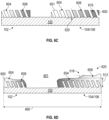
- FIGS. 5 A- 5 B are schematic sectional views of an overlayer during different stages of deposition and etching of the overlayer.
- FIG. 6 A- 6 D are schematic sectional views of a refractive body having various refractive indices during different stages of deposition and etching of the refractive body.
- FIGS. 7 A- 7 C are alternative examples of a head of the applicator shown in FIG. 4 .
- a measuring system is used to determine the amount of light entering an optical device.
- the optical device has an input coupling region, an intermediate region, and an output coupling region for exiting the amount of light, as in a waveguide combiner.
- the measuring system determines the amount of light entering a flat optical device, such as a waveguide having a metasurface with plural optical structures.
- the measuring system determines a profile of the light entering the optical device and the light exiting the optical device. Each of the input light and output light form a profile, which includes non-uniform light intensities.
- the apparatus and method disclosed herein includes expelling plasma from an applicator having a head toward a plurality of grating structures disposed on a substrate.
- the plasma is formed in the head at atmospheric pressure.
- a material layer overlays the substrate.
- the plasma has a reactant therein capable of reacting with, and thus removing, portions of a material layer, or a portion of the plurality of grating structures.
- the method includes changing a depth of the plurality of grating structures with the plasma by removing material therefrom.
- the applicator is movable with respect to the substrate, such that the plasma head is capable of being positioned over different discrete areas of the surface of the substrate, including over the material layer, or over the plurality of grating structures. Discrete portions of the material layer are etched by the plasma, in order to remove a portion of the material, and thereby form a three dimensional recess inwardly of the surface of the material.
- generating the two-dimensional surface profile can include etching gratings to change a height of the gratings of the waveguide combiner.
- generating the two-dimensional surface profile includes depositing an overlayer, such as an encapsulation layer.
- etching and deposition are used to create the two-dimensional surface profile.
- Conventional approaches to depositing an encapsulation layer or etching gratings include the use of one or more processing chambers to perform etching, deposition, and or photolithography. By utilizing an atmospheric pressure plasma jet (APPJ), precise control of grating depth, grating refractive index, and encapsulation thickness across the optical device are obtained in a manner not achievable by conventional approaches.
- APPJ atmospheric pressure plasma jet
- a diffraction efficiency of the optical device is increased by modifying a two-dimensional surface profile of an overlayer or a two-dimensional surface profile of gratings of the optical device, as disclosed herein.
- the two dimensional surface profile can be achieved at high throughput and at atmospheric pressure by etching and depositing with the APPJ.
- FIG. 1 is a schematic top view of an optical device 101 having a plurality of device structures.
- the substrate 100 described herein is a waveguide, in one example.
- the optical device 101 is a flat optical device, such as a metasurface that has a plurality of device structures.
- the optical device 101 is a waveguide combiner, such as an augmented reality waveguide combiner having a plurality of device structures.
- the device structures are nanostructures having sub-micron dimensions, e.g., nano-sized dimensions, such as critical dimensions less than 1 ⁇ m.
- the substrate 100 includes an input coupling region 102 defined by a plurality of gratings 108 , an intermediate region 104 defined by a plurality of gratings 110 , and an output coupling region 106 defined by a plurality of gratings 112 .
- the input coupling region 102 receives incident beams of light (a virtual image) having an intensity from a microdisplay.
- Each grating of the plurality of gratings 108 splits the incident beams into a plurality of modes, each beam having a mode.
- T0 beams are refracted back or lost in the substrate 100 (i.e., waveguide combiner), positive first-order mode (T1) beams are coupled though the substrate 100 to the intermediate region 104 , and negative first-order mode (T ⁇ 1) beams propagate in the substrate 100 at a direction opposite to the T1 beams.
- the incident beams are split into T1 beams that have all of the intensity of the incident beams in order to direct the virtual image to the intermediate region 104 .
- One approach to split the incident beam into T1 beams that have all of the intensity of the incident beams is to optimize the slant angle of each grating of the plurality of gratings 108 to suppress the T ⁇ 1 beams and the T0 beams.
- the T1 beams undergo total-internal-reflection (TIR) through the substrate 100 until the T1 beams come in contact with the plurality of gratings 110 in the intermediate region 104 .
- a portion of the input coupling region 102 may have gratings 108 with a slant angle different than the slant angle of gratings 108 from an adjacent portion of the input coupling region 102 .
- the T1 beams contact a grating of the plurality of gratings 110 .
- the T1 beams are split into T0 beams refracted back or lost in the substrate 100 , T1 beams that undergo TIR in the intermediate region 104 until the T1 beams contact another grating of the plurality of gratings 110 , and T ⁇ 1 beams that are coupled through the substrate 100 to the output coupling region 106 .
- the T1 beams that undergo TIR in the intermediate region 104 continue to contact gratings of the plurality of gratings 110 until either the intensity of the T1 beams coupled through the substrate 100 to the intermediate region 104 is depleted, or remaining T1 beams propagating through the intermediate region 104 reach the end of the intermediate region 104 .
- the plurality of gratings 110 must be tuned to control the T1 beams coupled through the substrate 100 to the intermediate region 104 in order to control the intensity of the T ⁇ 1 beams coupled to the output coupling region 106 to modulate a field of view of the virtual image produced from the microdisplay from a user's perspective and increase a viewing angle from which a user can view the virtual image.
- One approach to control the T1 beams coupled through the substrate 100 to the intermediate region 104 is to optimize the slant angle of each grating of the plurality of gratings 110 to control the intensity of the T ⁇ 1 beams coupled to the output coupling region 106 .
- a portion of the intermediate region 104 may have gratings 110 with a slant angle different than the slant angle of gratings 110 from an adjacent portion of the intermediate region 104 . Furthermore, the gratings 110 may have slant angles different than the slant angles of the gratings 108 .
- the T ⁇ 1 beams coupled through the substrate 100 to the output coupling region 106 undergo TIR in the substrate 100 until the T ⁇ 1 beams contact a grating of the plurality of gratings 112 where the T ⁇ 1 beams are split into T0 beams refracted back or lost in the substrate 100 , T1 beams that undergo TIR in the output coupling region 106 until the T1 beams contact another grating of the plurality of gratings 112 , and T ⁇ 1 beams coupled out of the substrate 100 .
- the applicator 404 includes a head 408 and a body 412 .
- the body 412 is electrically coupled to a power source 420 through one or more transmission lines 452 .
- the power source 420 is grounded.
- a gas source 416 is fluidly coupled to the body 412 , and is configured to provide a gas to an internal space of the body 412 .
- the gas provided to the internal space of the body 412 is one or more of argon (Ar), helium (He), nitrogen (N 2 ), oxygen (O 2 ), or hydrogen (H 2 ).
- a DC power of the applicator is between about 5 kV and about 15 kV, such as about 10 kV or 12 KV.
- the DC power of the applicator 404 is between about 10 kHz to about 100 kHz.
- An RF power is applied between about 300 watts and about 5 GHz, such as about 1 GHz, or about 2 GHz.
- the relative speed between the head 408 relative to the substrate 100 is between about 1 mm/s to about 30 mm/s, such as about 2.5 mm/s, or about 3.25 mm/s. In another example of the disclosure herein, the relative speed is about 5 mm/s to about 25 mm/s, such as about 17 mm/s or about 20.5 mm/s. In yet another example, the relative speed is between about 7.5 mm/s and about 15 mm/s, such as about 10 mm/s or about 12.5 mm/s.
- the plasma 424 is formed in the environment 401 when gas is introduced into the body 412 of the applicator 404 . Ions are created when the gas is disassociated within the plasma 424 by application of the power source 420 . The ions are expelled toward the substrate 100 , and upon impact with the gratings 308 , the ions remove molecules from the gratings 308 . A distance 456 from the head 408 of the applicator 404 to the substrate 100 is controlled by parameters of the target profile. The distance 456 to the substrate 100 is controlled to remove portions of the gratings 308 , until the target profile is achieved.
- the target profile can include each or both of an input profile 444 and an output profile 448 .
- the applicator 404 is an atmospheric pressure plasma jet (APPJ).
- the output profile 448 enables a light profile 454 to be uniform across the gratings 308 , thus reducing blur or other visual defects near the periphery of the gratings 308 .
- the output profile 448 increases the diffraction efficiency of the intermediate region 104 and the output coupling region 106 .
- the controller 428 signals to at least one or more electrodes (not shown) coupled to the body 412 of the applicator 404 , the gas source 416 , or the power source 420 .
- the controller 428 includes a processor 432 , a memory 436 , and support circuits 440 that are coupled to one another.
- the processor 432 may be one of any form of general purpose microprocessor, or a general purpose central processing unit (CPU), each of which can be used in an industrial setting, such as a programmable logic controller (PLC), supervisory control and data acquisition (SCADA) systems, or other suitable industrial controller.
- PLC programmable logic controller
- SCADA supervisory control and data acquisition
- the memory 436 is non-transitory and may be one or more of readily available memory such as random access memory (RAM), read only memory (ROM), or any other form of digital storage, local or remote.
- RAM random access memory
- ROM read only memory
- the memory 436 contains instructions, that when executed by the processor 432 , facilitates execution of the method 200 .
- the instructions in the memory 436 are in the form of a program product such as a program that implements the method of the present disclosure.
- the program code of the program product may conform to any one of a number of different programming languages.
- Illustrative computer-readable storage media include, but are not limited to: (i) non-writable storage media (e.g., read-only memory devices within a computer such as CD-ROM disks readable by a CD-ROM drive, flash memory, ROM chips, or any type of solid-state non-volatile semiconductor memory) on which information is permanently stored; and (ii) writable storage media (e.g., hard-disk drive or any type of solid-state random-access semiconductor memory) on which alterable information is stored.
- Such computer-readable storage media when carrying computer-readable instructions that direct the functions of the methods described herein, are examples of the present disclosure.
- Operation 212 can proceeded directly to Operation 216 , disclosed in detail below, as shown in FIG. 3 .
- the method 200 proceeds from Operation 208 to Operation 216 .
- an overlayer 500 is deposited over the substrate 100 at atmospheric pressure, as shown in FIG. 5 A .
- the overlayer 500 having a substantially planar surface 504 is deposited to a desired thickness over the substrate 100 .
- the overlayer 500 is an encapsulation layer.
- the encapsulation layer includes materials such as metals and dielectrics of varying dielectric constants and refractive indices. The encapsulation layer reduces glare or reflection on the substrate 100 .
- the overlayer 500 can be deposited to a depth 512 and a specified length 460 .
- the overlayer 500 is applied to gratings 308 with one of an FCVD, PVD or spin coating methods, in one example.
- plasma 424 is formed in the environment 401 by the applicator 404 in order to deposit the overlayer 500 .
- the overlayer 500 is formed by vaporizing a precursor with the plasma 424 .
- Exemplary materials for the overlayer 500 includes at least one of polyimides, polyimide blends, metal-organic polyimide blends, metal oxides, metal nitrides, Al 2 O 3 , SiO 2 , TiO, TaO, AlN, SiN, SiO x N x , TiN, TaN, any of the materials forming the substrate 100 or any one of the gratings 308 .
- the overlayer 500 herein enables control over diffraction efficiency along the gratings 308 .
- the low refractive index contrast of the overlayer 500 decreases the diffraction efficiency compared to un-encapsulated gratings (i.e., gratings without the overlayer 500 ).
- Device structures not having the overlayer 500 may be surrounded by air (i.e., refractive index of 1) contacting the surface or may include a global encapsulant having a low refractive index (e.g., refractive index contrast greater than about 0.2).
- the diffraction efficiency of the gratings 308 may be about 2.5% or less, alternatively from about 1% to about 50% such as from about 1% to about 40%, such as from about 1% to about 30%, such as from about 1% to about 20%, such as from about 1% to about 10%, such as from about 1% to about 5%, such as from about 1% to about 2.5%, alternatively from about 2.5% to about 5%, alternatively from about 5% to about 10%, alternatively from about 10% to about 20%, alternatively from about 20% to about 30%, alternatively from about 30% to about 40%, or alternatively from about 40% to about 50%.
- the overlayer 500 has a refractive index of from about 1.6 to about 2.4, such as from about 1.7 to about 2.3, such as from about 1.8 to about 2.2, such as from about 1.8 to about 2, such as from about 1.9 to about 2, or such as from about 1.95 to about 2.
- the overlayer 500 has a refractive index from about 2 to about 2.2, such as from about 2 to about 2.1, such as from about 2 to about 2.05, such as about 2, or alternatively from about 1.8 to about 1.85.
- the overlayer 500 has a refractive index from about 1.85 to about 1.9, alternatively from about 1.9 to about 1.95, alternatively from about 1.95 to about 1.96, alternatively from about 1.96 to about 1.97, or alternatively from about 1.97 to about 1.98.
- the overlayer 500 has a refractive index from about 1.98 to about 1.99, alternatively from about 1.99 to about 2, alternatively from about 2 to about 2.01, alternatively from about 2.01 to about 2.02, or alternatively from about 2.02 to about 2.03.
- Another exemplary refractive index of the overlayer 500 is from about 2.03 to about 2.04, alternatively from about 2.04 to about 2.05, alternatively from about 2.05 to about 2.1, alternatively from about 2.1 to about 2.2, or alternatively from about 1.95 to about 2.05.
- the overlayer 500 is a mask layer.
- the mask may be formed from a photoresist, a hard mask material or other suitable material.
- the photoresist may be a positive-tone photoresist and/or a negative-tone photoresist, each being capable of undergoing a chemically amplified reaction.
- the mask layer is an organic polymer material, in one example. Other suitable materials may be used for the mask, including other fluorine containing polymers.
- the mask can be at least one of a positive or negative tone photoresist, a metal-containing hardmask, a carbon-containing hardmask, an organic planarization layer (OPL), and other suitable hardmask materials.
- OPL organic planarization layer
- the overlayer 500 is a grayscale resist, or grayscale mask.
- the grayscale resist can be deposited in any pattern to produce the desired depth and shape of the substrate 100 .
- Gratings 308 of varying depth can be created using gray-tone lithography, also known as grayscale lithography.
- Grayscale lithography is a one-step process used to create three-dimensional microstructures in a photoresist layer using an optical gray-tone (or grayscale) mask. Grayscale masks let varying amounts of light pass through to create depth-modulated gratings 308 .
- Using grayscale lithography to create depth-modulated gratings 308 allows for fewer processing operations and increases wedge resolution of a surface profile 508 .
- the surface profile 508 can have a concave or convex pattern.
- a one-dimensional or two-dimensional grayscale mask pattern may be used to shape the grating height of the gratings 308 .
- each of the gratings 308 can have an angle 520 measured relative to the planar surface 504 .
- the angle 520 is, for example, about 0 degrees to about 70 degrees.
- portions of the overlayer 500 are removed by etching with plasma 424 from the applicator, at Operation 220 .
- the surface profile 508 corresponds to a refractive index of the overlayer 500 or substrate 100 .
- the surface profile 508 includes the depth 512 , surface angle 516 , and length 460 parameters. Additional parameters such as the distance 456 from the head 408 of the applicator 404 to the substrate 100 (as shown in FIG. 4 ) are controlled to etch the overlayer 500 until the surface profile 508 is achieved.
- adjusting parameters such as plasma power and speed of the applicator 404 relative to the length 460 of the substrate 100 , can also be adjusted to create the surface profile 508 .
- the surface profile 508 can include portions having linear or non-linear slopes (i.e., a non-linear gradation) with respect to the substrate 100 . Additionally, the surface profile 508 can include several portions that oscillate with respect to the substrate 100 .
- a refractive body 600 is deposited on the substrate 100 at atmospheric pressure.
- the refractive body 600 has a planar surface 601 and includes a first refractive layer 604 and a second refractive layer 608 .
- the second refractive layer 608 is shown as a single feature, the second refractive layer 608 can include additional refractive layers. As such, the second refractive layer 608 can include additional individual layers having different refractive indices. Accordingly, the change in the composition of refractive body 600 from first refractive layer 604 to the second refractive layer 608 is gradual.
- the refractive body 600 is deposited such that no distinct or visible layers are observed between the first refractive layer 604 and the second refractive layer 608 .
- the refractive index of the refractive body 600 gradually modulates independently of the thickness of the refractive body 600 .
- the refractive indices of the refractive body 600 modulate along the length 460 of the substrate 100 .
- the refractive indices of the refractive body 600 modulate in a direction perpendicular to the length 460 .
- the diffraction efficiency of the refractive body 600 is modified by applying different materials during deposition of the refractive layers 604 , 608 .
- FIGS. 6 A- 6 D are schematic sectional views of the substrate 100 during deposition and removal of an overlayer having different refractive indices.
- One or more gases from the gas source 416 are flowed into the environment 401 to deposit the refractive body 600 (i.e., the first refractive layer 604 and the second refractive layer 608 ) onto the substrate 100 using the applicator 404 .
- Exemplary precursor gases include nitrogen gas (N 2 ), nitrogen dioxide (NO 2 ), fluorine gas (F 2 ), oxygen gas (O 2 ), hydrogen gas (H2), H 2 O in vapor form, methane (CH4), carbon monoxide (CO), methane (CH 4 ), and carbon dioxide (CO 2 ), argon (Ar), and helium (He).
- the first refractive layer 604 may be a sol-gel solution or a nanoparticle solution.
- the first solution may include silicon dioxide (SiO 2 ), silicon oxycarbide (SiOC), zirconium dioxide (ZrO 2 ), and/or titanium dioxide (TiO 2 ). Proportions of SiO 2 , SiOC, ZrO 2 , and/or TiO 2 in the first solution are controlled to result in a first refractive index.
- the first solution may contain a first ratio of TiO 2 to SiO 2 , SiOC, and/or ZrO 2 .
- sol-gel precursors for SiO 2 may include tetramethyl orthosilicate (TMOS), methyl-tri-methoxy-silane (MTMS), and tetraethyl orthosilicate (TEOS).
- the second refractive layer 608 may include a second solution.
- the second solution may be a sol-gel solution or a nanoparticle solution.
- the second solution may include SiO 2 , SiOC, ZrO 2 , and/or TiO 2 . Proportions of SiO 2 , SiOC, ZrO 2 , and/or TiO 2 in the second solution are controlled to result in a second refractive index.
- the second refractive index may be different than the first refractive index.
- the second solution may contain a second ratio having a higher ratio of TiO 2 to SiO 2 , SiOC, and/or ZrO 2 than the first ratio to result in the second refractive index having a higher refractive index than the first refractive index or the second ratio may have a lower ratio of TiO 2 to SiO 2 , SiOC, and/or ZrO 2 than the first ratio to result in the second refractive index having a lower refractive index than the first refractive index.
- a first refractive layer may include a first material, and a subsequent refractive layer may include a second material different from the first material.
- the refractive index of the encapsulation layer can be tuned from over about 2.0 to about 1.47. Exemplary ranges for the refractive index of the refractive body 600 can be between about 1.5 and about 2.0, for example about 1.75. In yet other example, the refractive index of the refractive body 600 can between about 1.0 and about 1.5, for example about 1.47. In yet another example, the refractive index of the refractive body 600 can be between about 1.0 and about 1.5, for example about 1.48 or about 1.49; or between about 1.0 and about 1.5, for example about 1.47.
- Each of the first refractive layer and subsequent refractive layer(s), such as the second refractive layer, can have a refractive index of from about 1.6 to about 2.4, such as from about 1.7 to about 2.3, such as from about 1.8 to about 2.2, such as from about 1.8 to about 2, such as from about 1.9 to about 2, such as from about 1.95 to about 2.
- the overlayer 500 has a refractive index from about 2 to about 2.2, such as from about 2 to about 2.1, such as from about 2 to about 2.05, such as about 2, alternatively from about 1.8 to about 1.85.
- the overlayer 500 has a refractive index from about 1.85 to about 1.9, alternatively from about 1.9 to about 1.95, alternatively from about 1.95 to about 1.96, alternatively from about 1.96 to about 1.97, alternatively from about 1.97 to about 1.98.
- the overlayer 500 has a refractive index from about 1.98 to about 1.99, alternatively from about 1.99 to about 2, alternatively from about 2 to about 2.01, alternatively from about 2.01 to about 2.02, alternatively from about 2.02 to about 2.03.
- Another exemplary refractive index of the overlayer 500 is from about 2.03 to about 2.04, alternatively from about 2.04 to about 2.05, alternatively from about 2.05 to about 2.1, alternatively from about 2.1 to about 2.2, alternatively from about 1.95 to about 2.05.
- an overlayer 500 is formed over and in contact with the refractive body 600 .
- the overlayer 500 can be a mask layer deposited in contact with and over the refractive body 600 using the applicator 404 .
- the refractive index pattern is programed into to the controller 428 in order to match the target profile. Openings 612 are made through the overlayer 500 , exposing a portion of the planar surface 601 of the refractive body 600 .
- the overlayer 500 can be deposited by FCVD, PVD, spin coating, or deposited by ignited plasma 424 from the applicator 404 in the environment 401 .
- lithography is performed to transfer a pattern into the refractive body 600 .
- a material of the mask layer includes any hard mask material, such as photoresist, SiO 2 , Cr.
- the refractive body 600 is etched using the applicator 404 .
- An etch process can be performed, as described above at Operation 212 or at Operation 220 , in order to remove portions of the refractive body 600 thus forming graduated refractive gratings 616 of varying refractive indices, as shown in FIG. 6 C .
- the gratings 308 include portions of the first refractive layer 604 and the second refractive layer 608 .
- the second refractive layer 608 can include additional individual layers of varying refractive indices.
- each of the gratings 308 can have an angle 520 measured relative to the planar surface 601 .
- the angle 520 can be, for example, about 0 degrees to about 80 degrees, such as about 70 degrees. In another example, the angle 520 is between about 5 degrees and about 65 degrees, such as about 45 degrees, or about 55 degrees.
- a surface profile 620 having a modulating refractive index is formed in the refractive body 600 .
- the surface profile 620 is based upon the target profile described above.
- Plasma 424 is utilized to etch the surface profile 620 into the planar surface 601 of the refractive body 600 .
- the refractive body 600 includes the first refractive layer 604 and the second refractive layer 608 .
- the surface profile 620 includes a depth 512 , surface angle 516 , and the length 460 parameters.
- the distance 456 from the head 408 of the applicator 404 to the substrate 100 , plasma power, and a speed of the applicator 404 relative to the length 460 of the substrate 100 can also be adjusted to create the surface profile 620 .
- the surface profile 620 can include portions having linear or non-linear slopes, and can include several portions that oscillate with respect to the substrate 100 . In one example, the surface profile 620 includes a portion this is hydrophobic and another portion that is hydrophilic.
- the refractive body 600 is deposited at Operation 224 and an overlayer 500 is deposited at Operation 216 . The method 200 can then proceed to Operation 220 where the overlayer 500 is etched.
- the openings 612 are formed in the overlayer 500 through photolithography.
- the method then proceeds to Operation 228 where the refractive body 600 is etched.
- the graduated refractive gratings 616 are formed as shown in FIG. 6 C .
- the surface profile 620 is formed as shown in FIG. 6 D .
- the refractive body 600 is deposited with the surface profile 620 , in substantially the same manner as the refractive body 600 is deposited, as shown in FIG. 6 A , or the overlayer 500 , as shown in FIG. 5 A-B .
- the method 200 returns to Operation 212 .
- the gratings 308 are etched, and in another example, the graduated refractive gratings 616 are etched.
- the method 200 is repeated until the gratings 308 reach the target profile thus producing uniform light profile 454 .
- the method 200 is repeated until the target profile is achieved and uniform light profile 454 exits the graduated refractive gratings 616 .
- Operation 216 or Operation 224 can proceed to Operation 232 .
- the method 200 at Operation 232 returns directly to Operation 224 , and a subsequent layer of the second refractive layer 608 is deposited. The method 200 is repeated until the refractive body 600 has a desired refractive index. In yet another example, the method 200 at Operation 232 returns to Operation 220 where another portion of the overlayer 500 is etched having the surface profile 508 . The method 200 is repeated until the overlayer 508 has the desired surface profile 508 . The method 200 can also be repeated until the refractive body 600 has the desired surface profile 620 , in yet another example.
- FIGS. 7 A- 7 C are alternative examples of the head 408 of the applicator 404 shown in FIG. 4 .
- the head 408 is a nozzle 704 having an opening 716 through which the jet of the plasma 424 is expelled, as shown in FIG. 7 A .
- the head 408 is a quadrilateral head 708 having a rectangular opening 720 .
- the quadrilateral head 708 has a substantially rectangular perimeter, but is not limited to this arrangement.
- quadrilateral head 708 is substantially square.
- the head 408 is an array 712 , the array 712 having n x m openings 716 .
- a 4 ⁇ 5 array 712 of openings 716 is shown, in a non-limiting example.
- the disclosure herein is not limited to that arrangement and includes arrays where a value of n is not equal to a value of m, such as a 5 ⁇ 4, 2 ⁇ 3, or 5 ⁇ 9 array of openings 716 .
- Exemplary arrays 712 also include square arrays where a value of n is equal to a value of m, such as a 3 ⁇ 3, 5 ⁇ 5, or a 10 ⁇ 10 array of openings 716 .
- Each of the nozzle 704 , the quadrilateral head 708 , and the array 712 can be utilized with the method 200 to achieve the target profile, as disclosed herein.
Landscapes
- Physics & Mathematics (AREA)
- General Physics & Mathematics (AREA)
- Optics & Photonics (AREA)
- Engineering & Computer Science (AREA)
- Plasma & Fusion (AREA)
- Mechanical Engineering (AREA)
- Manufacturing & Machinery (AREA)
- Diffracting Gratings Or Hologram Optical Elements (AREA)
- Optical Integrated Circuits (AREA)
Priority Applications (1)
| Application Number | Priority Date | Filing Date | Title |
|---|---|---|---|
| US17/455,288 US12109641B2 (en) | 2020-11-17 | 2021-11-17 | Optical device having structural and refractive index gradation, and method of fabricating the same |
Applications Claiming Priority (2)
| Application Number | Priority Date | Filing Date | Title |
|---|---|---|---|
| US202063114919P | 2020-11-17 | 2020-11-17 | |
| US17/455,288 US12109641B2 (en) | 2020-11-17 | 2021-11-17 | Optical device having structural and refractive index gradation, and method of fabricating the same |
Publications (2)
| Publication Number | Publication Date |
|---|---|
| US20220152724A1 US20220152724A1 (en) | 2022-05-19 |
| US12109641B2 true US12109641B2 (en) | 2024-10-08 |
Family
ID=81588122
Family Applications (1)
| Application Number | Title | Priority Date | Filing Date |
|---|---|---|---|
| US17/455,288 Active 2043-01-24 US12109641B2 (en) | 2020-11-17 | 2021-11-17 | Optical device having structural and refractive index gradation, and method of fabricating the same |
Country Status (6)
| Country | Link |
|---|---|
| US (1) | US12109641B2 (de) |
| EP (1) | EP4248262A4 (de) |
| KR (1) | KR102856854B1 (de) |
| CN (1) | CN117063104A (de) |
| TW (1) | TWI876108B (de) |
| WO (1) | WO2022108986A1 (de) |
Families Citing this family (6)
| Publication number | Priority date | Publication date | Assignee | Title |
|---|---|---|---|---|
| US12140802B2 (en) * | 2021-05-28 | 2024-11-12 | Taiwan Semiconductor Manufacturing Co., Ltd. | 1D apodized grating devices and methods for suppressing optical noise |
| CN114994918A (zh) * | 2022-06-17 | 2022-09-02 | 京东方科技集团股份有限公司 | 一种光波导镜片及其封装方法 |
| WO2024064196A1 (en) * | 2022-09-20 | 2024-03-28 | Applied Materials, Inc. | Method for integration of optical device fabrication with substrate thickness engineering |
| US12416755B2 (en) | 2023-03-14 | 2025-09-16 | Adeia Guides Inc. | Refractive index modulation in diffractive gratings for optical elements of augmented reality and virtual reality displays |
| US20250123489A1 (en) * | 2023-10-16 | 2025-04-17 | Microsoft Technology Licensing, Llc | Mixed-reality waveguide combiner with gradient refractive index gratings |
| WO2026064274A1 (en) * | 2024-09-18 | 2026-03-26 | Applied Materials, Inc. | Improved image contrast of waveguide combiners by engineering internal loss |
Citations (30)
| Publication number | Priority date | Publication date | Assignee | Title |
|---|---|---|---|---|
| US5734143A (en) * | 1994-10-26 | 1998-03-31 | Matsushita Electric Industrial Co., Ltd. | Microwave plasma torch having discretely positioned gas injection holes and method for generating plasma |
| US20030210880A1 (en) * | 2001-07-12 | 2003-11-13 | Johnson Frederick G. | Use of deuterated gases for the vapor deposition of thin films for low-loss optical devices and waveguides |
| JP2005246667A (ja) * | 2004-03-02 | 2005-09-15 | Matsushita Electric Ind Co Ltd | 金型のクリーニング方法及び装置、成型方法及び装置 |
| US20100078320A1 (en) | 2008-09-26 | 2010-04-01 | Applied Materials, Inc. | Microwave plasma containment shield shaping |
| US20110151270A1 (en) * | 2009-12-18 | 2011-06-23 | Todd Jay Rockstroh | Methods of laser assisted plasma coating at atmospheric pressure and superalloy substrates comprising coatings made using the same |
| US20120009724A1 (en) | 2010-07-08 | 2012-01-12 | Seung-Yeop Myong | Method for handling a flexible substrate of solar cell |
| US20120261391A1 (en) * | 2009-10-06 | 2012-10-18 | Fraunhofer-Gesellschaft zur Förderung der angewandten Forschung e.V. | Atmospheric pressure plasma method for producing surface-modified particles and coatings |
| DE102013220841A1 (de) * | 2013-10-15 | 2015-04-16 | Plasmatreat Gmbh | Verfahren zur Vorbehandlung einer Substratoberfläche und Verfahren zur Beschichtung der Substratoberfläche |
| US9329325B2 (en) * | 2009-04-20 | 2016-05-03 | Bae Systems Plc | Optical waveguides |
| US20170315346A1 (en) * | 2016-04-29 | 2017-11-02 | Jani Kari Tapio Tervo | Robust Architecture for Large Field of View Components |
| US20180081265A1 (en) * | 2016-09-21 | 2018-03-22 | Molecular Imprints, Inc. | Microlithographic fabrication of structures |
| US20180149796A1 (en) * | 2016-11-30 | 2018-05-31 | Molecular Imprints, Inc. | Multi-waveguide light field display |
| KR20180100044A (ko) * | 2015-08-17 | 2018-09-06 | 온토스 이큅먼트 시스템즈 | 상압 플라즈마 처리 단계들을 이용한 에피택셜 성장 |
| WO2019180841A1 (ja) * | 2018-03-20 | 2019-09-26 | 株式会社Fuji | プラズマ装置、プラズマヘッド用ダミーノズル |
| US10442727B2 (en) * | 2017-01-05 | 2019-10-15 | Magic Leap, Inc. | Patterning of high refractive index glasses by plasma etching |
| US20200110278A1 (en) * | 2017-11-06 | 2020-04-09 | Magic Leap, Inc. | Method and system for tunable gradient patterning using a shadow mask |
| US20200124865A1 (en) | 2018-10-23 | 2020-04-23 | Applied Materials, Inc. | Optical component having depth modulated angled gratings and method of formation |
| US20200142120A1 (en) | 2018-11-07 | 2020-05-07 | Applied Materials, Inc. | Depth-modulated slanted gratings using gray-tone lithography and slant etch |
| US20200194218A1 (en) | 2018-12-17 | 2020-06-18 | Applied Materials, Inc. | Methods of optical device fabrication using an electron beam apparatus |
| US20200258717A1 (en) * | 2017-10-01 | 2020-08-13 | Space Foundry Inc. | Modular print head assembly for plasma jet printing |
| US20200301062A1 (en) | 2017-11-29 | 2020-09-24 | Applied Materials, Inc. | Method of direct etching fabrication of waveguide combiners |
| WO2020210425A1 (en) | 2019-04-11 | 2020-10-15 | Applied Materials, Inc. | Patterning of multi-depth optical devices |
| US20200332414A1 (en) | 2019-04-16 | 2020-10-22 | Applied Materials, Inc. | Mehtod of thin film deposition in trenches |
| US20200363719A1 (en) | 2019-05-15 | 2020-11-19 | Applied Materials, Inc. | Methods of forming variable-depth device structures |
| US10935730B1 (en) * | 2019-11-25 | 2021-03-02 | Shanghai North Ocean Photonics Co., Ltd. | Waveguide display device |
| US10955606B2 (en) | 2018-05-30 | 2021-03-23 | Applied Materials, Inc. | Method of imprinting tilt angle light gratings |
| US20210157148A1 (en) * | 2019-11-25 | 2021-05-27 | Shanghai North Ocean Photonics Co., Ltd. | Waveguide Display Device |
| WO2021150311A1 (en) | 2020-01-22 | 2021-07-29 | Applied Materials, Inc. | High refractive index imprint compositions and materials and processes for making the same |
| US20210325777A1 (en) | 2020-04-20 | 2021-10-21 | Applied Materials, Inc. | Methods for increasing the refractive index of high-index nanoimprint lithography films |
| US20220026603A1 (en) | 2020-07-22 | 2022-01-27 | Applied Materials, Inc. | Method for deposition of depth-varying refractive index films |
Family Cites Families (5)
| Publication number | Priority date | Publication date | Assignee | Title |
|---|---|---|---|---|
| JP6972121B2 (ja) * | 2016-10-05 | 2021-11-24 | マジック リープ, インコーポレイテッドMagic Leap, Inc. | 不均一回折格子の加工 |
| CN108873350A (zh) * | 2018-07-24 | 2018-11-23 | 上海鲲游光电科技有限公司 | 一种波导显示装置 |
| JP7579247B2 (ja) | 2018-11-16 | 2024-11-07 | マジック リープ, インコーポレイテッド | 接眼レンズのための重畳された回折格子 |
| EP3938824A4 (de) * | 2019-03-12 | 2022-11-23 | Magic Leap, Inc. | Wellenleiter mit materialien mit hohem brechungsindex und verfahren zu deren herstellung |
| US12117630B2 (en) * | 2019-03-12 | 2024-10-15 | Magic Leap, Inc. | Method of fabricating display device having patterned lithium-based transition metal oxide |
-
2021
- 2021-11-17 WO PCT/US2021/059654 patent/WO2022108986A1/en not_active Ceased
- 2021-11-17 CN CN202180081225.2A patent/CN117063104A/zh active Pending
- 2021-11-17 TW TW110142792A patent/TWI876108B/zh active
- 2021-11-17 KR KR1020237020206A patent/KR102856854B1/ko active Active
- 2021-11-17 US US17/455,288 patent/US12109641B2/en active Active
- 2021-11-17 EP EP21895485.7A patent/EP4248262A4/de active Pending
Patent Citations (33)
| Publication number | Priority date | Publication date | Assignee | Title |
|---|---|---|---|---|
| US5734143A (en) * | 1994-10-26 | 1998-03-31 | Matsushita Electric Industrial Co., Ltd. | Microwave plasma torch having discretely positioned gas injection holes and method for generating plasma |
| US20030210880A1 (en) * | 2001-07-12 | 2003-11-13 | Johnson Frederick G. | Use of deuterated gases for the vapor deposition of thin films for low-loss optical devices and waveguides |
| JP2005246667A (ja) * | 2004-03-02 | 2005-09-15 | Matsushita Electric Ind Co Ltd | 金型のクリーニング方法及び装置、成型方法及び装置 |
| US20100078320A1 (en) | 2008-09-26 | 2010-04-01 | Applied Materials, Inc. | Microwave plasma containment shield shaping |
| US9329325B2 (en) * | 2009-04-20 | 2016-05-03 | Bae Systems Plc | Optical waveguides |
| US20120261391A1 (en) * | 2009-10-06 | 2012-10-18 | Fraunhofer-Gesellschaft zur Förderung der angewandten Forschung e.V. | Atmospheric pressure plasma method for producing surface-modified particles and coatings |
| US20110151270A1 (en) * | 2009-12-18 | 2011-06-23 | Todd Jay Rockstroh | Methods of laser assisted plasma coating at atmospheric pressure and superalloy substrates comprising coatings made using the same |
| US20120009724A1 (en) | 2010-07-08 | 2012-01-12 | Seung-Yeop Myong | Method for handling a flexible substrate of solar cell |
| DE102013220841A1 (de) * | 2013-10-15 | 2015-04-16 | Plasmatreat Gmbh | Verfahren zur Vorbehandlung einer Substratoberfläche und Verfahren zur Beschichtung der Substratoberfläche |
| KR20180100044A (ko) * | 2015-08-17 | 2018-09-06 | 온토스 이큅먼트 시스템즈 | 상압 플라즈마 처리 단계들을 이용한 에피택셜 성장 |
| US20170315346A1 (en) * | 2016-04-29 | 2017-11-02 | Jani Kari Tapio Tervo | Robust Architecture for Large Field of View Components |
| US20180081265A1 (en) * | 2016-09-21 | 2018-03-22 | Molecular Imprints, Inc. | Microlithographic fabrication of structures |
| US20200124782A1 (en) * | 2016-11-30 | 2020-04-23 | Molecular Imprints, Inc. | Multi-waveguide light field display |
| US20180149796A1 (en) * | 2016-11-30 | 2018-05-31 | Molecular Imprints, Inc. | Multi-waveguide light field display |
| US20220035091A1 (en) * | 2016-11-30 | 2022-02-03 | Molecular Imprints, Inc. | Multi-waveguide light field display |
| US10442727B2 (en) * | 2017-01-05 | 2019-10-15 | Magic Leap, Inc. | Patterning of high refractive index glasses by plasma etching |
| US20200258717A1 (en) * | 2017-10-01 | 2020-08-13 | Space Foundry Inc. | Modular print head assembly for plasma jet printing |
| US20200110278A1 (en) * | 2017-11-06 | 2020-04-09 | Magic Leap, Inc. | Method and system for tunable gradient patterning using a shadow mask |
| US20200301062A1 (en) | 2017-11-29 | 2020-09-24 | Applied Materials, Inc. | Method of direct etching fabrication of waveguide combiners |
| WO2019180841A1 (ja) * | 2018-03-20 | 2019-09-26 | 株式会社Fuji | プラズマ装置、プラズマヘッド用ダミーノズル |
| US10955606B2 (en) | 2018-05-30 | 2021-03-23 | Applied Materials, Inc. | Method of imprinting tilt angle light gratings |
| US20200124865A1 (en) | 2018-10-23 | 2020-04-23 | Applied Materials, Inc. | Optical component having depth modulated angled gratings and method of formation |
| US20200142120A1 (en) | 2018-11-07 | 2020-05-07 | Applied Materials, Inc. | Depth-modulated slanted gratings using gray-tone lithography and slant etch |
| US20200194218A1 (en) | 2018-12-17 | 2020-06-18 | Applied Materials, Inc. | Methods of optical device fabrication using an electron beam apparatus |
| WO2020210425A1 (en) | 2019-04-11 | 2020-10-15 | Applied Materials, Inc. | Patterning of multi-depth optical devices |
| US20200332414A1 (en) | 2019-04-16 | 2020-10-22 | Applied Materials, Inc. | Mehtod of thin film deposition in trenches |
| US20200363719A1 (en) | 2019-05-15 | 2020-11-19 | Applied Materials, Inc. | Methods of forming variable-depth device structures |
| US10935730B1 (en) * | 2019-11-25 | 2021-03-02 | Shanghai North Ocean Photonics Co., Ltd. | Waveguide display device |
| US20210157148A1 (en) * | 2019-11-25 | 2021-05-27 | Shanghai North Ocean Photonics Co., Ltd. | Waveguide Display Device |
| WO2021150311A1 (en) | 2020-01-22 | 2021-07-29 | Applied Materials, Inc. | High refractive index imprint compositions and materials and processes for making the same |
| US20210325777A1 (en) | 2020-04-20 | 2021-10-21 | Applied Materials, Inc. | Methods for increasing the refractive index of high-index nanoimprint lithography films |
| US20220026603A1 (en) | 2020-07-22 | 2022-01-27 | Applied Materials, Inc. | Method for deposition of depth-varying refractive index films |
| WO2022020101A1 (en) | 2020-07-22 | 2022-01-27 | Applied Materials, Inc. | Method for deposition of depth-varying refractive index films |
Non-Patent Citations (2)
| Title |
|---|
| International Search Report and Written Opinion dated Mar. 14, 2022 for Application No. PCT/US2021/059654. |
| Jeong et. al., "Etching materials with an atmospheric-pressure plasma jet" Plasma Sources Sci. Technol. 7, 1998, pp. 282-285 (Year: 1998). * |
Also Published As
| Publication number | Publication date |
|---|---|
| TW202235931A (zh) | 2022-09-16 |
| US20220152724A1 (en) | 2022-05-19 |
| KR20230104728A (ko) | 2023-07-10 |
| KR102856854B1 (ko) | 2025-09-05 |
| TWI876108B (zh) | 2025-03-11 |
| CN117063104A (zh) | 2023-11-14 |
| EP4248262A4 (de) | 2024-11-13 |
| WO2022108986A1 (en) | 2022-05-27 |
| EP4248262A1 (de) | 2023-09-27 |
Similar Documents
| Publication | Publication Date | Title |
|---|---|---|
| US12109641B2 (en) | Optical device having structural and refractive index gradation, and method of fabricating the same | |
| US12130465B2 (en) | Variable height slanted grating method | |
| US11372149B2 (en) | Depth-modulated slanted gratings using gray-tone lithography and slant etch | |
| US11231540B2 (en) | Anisotropically formed diffraction grating device | |
| US11391950B2 (en) | Techniques for controlling effective refractive index of gratings | |
| US11137536B2 (en) | Bragg-like gratings on high refractive index material | |
| EP3878007B1 (de) | Bildung von winkelgittern | |
| US20200192009A1 (en) | Methods of producing slanted gratings | |
| KR102779144B1 (ko) | 플라즈마 에칭에 의한 고굴절률 유리들의 패터닝 | |
| JP7693646B2 (ja) | 回折格子を加工する方法 | |
| EP3743754A1 (de) | Steuerung der gitterauskopplungsstärke für ar-wellenleiter-kombinierer | |
| TW202349064A (zh) | 用於超高解析度相位延遲和波前塑形的多層平坦透鏡 | |
| US20220397708A1 (en) | Method of etching surface-relief structures | |
| US11581189B2 (en) | Controlled hardmask shaping to create tapered slanted fins | |
| KR102606558B1 (ko) | 광학적 격자 컴포넌트를 생성하는 방법 | |
| US20230057283A1 (en) | Surface relief grating and method of making the same | |
| US20250067927A1 (en) | Optical phased array fiber coupler | |
| US20230384596A1 (en) | Method to improve display efficiency and uniformity of ar waveguide | |
| WO2025111375A1 (en) | Waveguide designs with low eye-glow and high efficiency | |
| WO2022261374A1 (en) | Method of etching surface-relief structures |
Legal Events
| Date | Code | Title | Description |
|---|---|---|---|
| FEPP | Fee payment procedure |
Free format text: ENTITY STATUS SET TO UNDISCOUNTED (ORIGINAL EVENT CODE: BIG.); ENTITY STATUS OF PATENT OWNER: LARGE ENTITY |
|
| STPP | Information on status: patent application and granting procedure in general |
Free format text: DOCKETED NEW CASE - READY FOR EXAMINATION |
|
| AS | Assignment |
Owner name: APPLIED MATERIALS, INC., CALIFORNIA Free format text: ASSIGNMENT OF ASSIGNORS INTEREST;ASSIGNORS:LUO, KANG;GODET, LUDOVIC;ZHANG, DAIHUA;AND OTHERS;SIGNING DATES FROM 20201119 TO 20201123;REEL/FRAME:059942/0543 |
|
| STPP | Information on status: patent application and granting procedure in general |
Free format text: NON FINAL ACTION MAILED |
|
| STPP | Information on status: patent application and granting procedure in general |
Free format text: RESPONSE TO NON-FINAL OFFICE ACTION ENTERED AND FORWARDED TO EXAMINER |
|
| STPP | Information on status: patent application and granting procedure in general |
Free format text: FINAL REJECTION MAILED |
|
| STPP | Information on status: patent application and granting procedure in general |
Free format text: RESPONSE AFTER FINAL ACTION FORWARDED TO EXAMINER |
|
| STPP | Information on status: patent application and granting procedure in general |
Free format text: NOTICE OF ALLOWANCE MAILED -- APPLICATION RECEIVED IN OFFICE OF PUBLICATIONS |
|
| ZAAB | Notice of allowance mailed |
Free format text: ORIGINAL CODE: MN/=. |
|
| STPP | Information on status: patent application and granting procedure in general |
Free format text: PUBLICATIONS -- ISSUE FEE PAYMENT VERIFIED |
|
| STCF | Information on status: patent grant |
Free format text: PATENTED CASE |