US12094409B2 - Pixel circuitry and driving method thereof, array substrate and display panel - Google Patents
Pixel circuitry and driving method thereof, array substrate and display panel Download PDFInfo
- Publication number
- US12094409B2 US12094409B2 US18/044,114 US202118044114A US12094409B2 US 12094409 B2 US12094409 B2 US 12094409B2 US 202118044114 A US202118044114 A US 202118044114A US 12094409 B2 US12094409 B2 US 12094409B2
- Authority
- US
- United States
- Prior art keywords
- circuit
- node
- signal
- transistor
- light emission
- Prior art date
- Legal status (The legal status is an assumption and is not a legal conclusion. Google has not performed a legal analysis and makes no representation as to the accuracy of the status listed.)
- Active
Links
Images


Classifications
-
- G—PHYSICS
- G09—EDUCATION; CRYPTOGRAPHY; DISPLAY; ADVERTISING; SEALS
- G09G—ARRANGEMENTS OR CIRCUITS FOR CONTROL OF INDICATING DEVICES USING STATIC MEANS TO PRESENT VARIABLE INFORMATION
- G09G3/00—Control arrangements or circuits, of interest only in connection with visual indicators other than cathode-ray tubes
- G09G3/20—Control arrangements or circuits, of interest only in connection with visual indicators other than cathode-ray tubes for presentation of an assembly of a number of characters, e.g. a page, by composing the assembly by combination of individual elements arranged in a matrix no fixed position being assigned to or needed to be assigned to the individual characters or partial characters
- G09G3/22—Control arrangements or circuits, of interest only in connection with visual indicators other than cathode-ray tubes for presentation of an assembly of a number of characters, e.g. a page, by composing the assembly by combination of individual elements arranged in a matrix no fixed position being assigned to or needed to be assigned to the individual characters or partial characters using controlled light sources
- G09G3/30—Control arrangements or circuits, of interest only in connection with visual indicators other than cathode-ray tubes for presentation of an assembly of a number of characters, e.g. a page, by composing the assembly by combination of individual elements arranged in a matrix no fixed position being assigned to or needed to be assigned to the individual characters or partial characters using controlled light sources using electroluminescent panels
- G09G3/32—Control arrangements or circuits, of interest only in connection with visual indicators other than cathode-ray tubes for presentation of an assembly of a number of characters, e.g. a page, by composing the assembly by combination of individual elements arranged in a matrix no fixed position being assigned to or needed to be assigned to the individual characters or partial characters using controlled light sources using electroluminescent panels semiconductive, e.g. using light-emitting diodes [LED]
- G09G3/3208—Control arrangements or circuits, of interest only in connection with visual indicators other than cathode-ray tubes for presentation of an assembly of a number of characters, e.g. a page, by composing the assembly by combination of individual elements arranged in a matrix no fixed position being assigned to or needed to be assigned to the individual characters or partial characters using controlled light sources using electroluminescent panels semiconductive, e.g. using light-emitting diodes [LED] organic, e.g. using organic light-emitting diodes [OLED]
- G09G3/3225—Control arrangements or circuits, of interest only in connection with visual indicators other than cathode-ray tubes for presentation of an assembly of a number of characters, e.g. a page, by composing the assembly by combination of individual elements arranged in a matrix no fixed position being assigned to or needed to be assigned to the individual characters or partial characters using controlled light sources using electroluminescent panels semiconductive, e.g. using light-emitting diodes [LED] organic, e.g. using organic light-emitting diodes [OLED] using an active matrix
- G09G3/3233—Control arrangements or circuits, of interest only in connection with visual indicators other than cathode-ray tubes for presentation of an assembly of a number of characters, e.g. a page, by composing the assembly by combination of individual elements arranged in a matrix no fixed position being assigned to or needed to be assigned to the individual characters or partial characters using controlled light sources using electroluminescent panels semiconductive, e.g. using light-emitting diodes [LED] organic, e.g. using organic light-emitting diodes [OLED] using an active matrix with pixel circuitry controlling the current through the light-emitting element
-
- G—PHYSICS
- G09—EDUCATION; CRYPTOGRAPHY; DISPLAY; ADVERTISING; SEALS
- G09G—ARRANGEMENTS OR CIRCUITS FOR CONTROL OF INDICATING DEVICES USING STATIC MEANS TO PRESENT VARIABLE INFORMATION
- G09G2300/00—Aspects of the constitution of display devices
- G09G2300/08—Active matrix structure, i.e. with use of active elements, inclusive of non-linear two terminal elements, in the pixels together with light emitting or modulating elements
- G09G2300/0809—Several active elements per pixel in active matrix panels
- G09G2300/0819—Several active elements per pixel in active matrix panels used for counteracting undesired variations, e.g. feedback or autozeroing
-
- G—PHYSICS
- G09—EDUCATION; CRYPTOGRAPHY; DISPLAY; ADVERTISING; SEALS
- G09G—ARRANGEMENTS OR CIRCUITS FOR CONTROL OF INDICATING DEVICES USING STATIC MEANS TO PRESENT VARIABLE INFORMATION
- G09G2300/00—Aspects of the constitution of display devices
- G09G2300/08—Active matrix structure, i.e. with use of active elements, inclusive of non-linear two terminal elements, in the pixels together with light emitting or modulating elements
- G09G2300/0809—Several active elements per pixel in active matrix panels
- G09G2300/0842—Several active elements per pixel in active matrix panels forming a memory circuit, e.g. a dynamic memory with one capacitor
- G09G2300/0852—Several active elements per pixel in active matrix panels forming a memory circuit, e.g. a dynamic memory with one capacitor being a dynamic memory with more than one capacitor
-
- G—PHYSICS
- G09—EDUCATION; CRYPTOGRAPHY; DISPLAY; ADVERTISING; SEALS
- G09G—ARRANGEMENTS OR CIRCUITS FOR CONTROL OF INDICATING DEVICES USING STATIC MEANS TO PRESENT VARIABLE INFORMATION
- G09G2300/00—Aspects of the constitution of display devices
- G09G2300/08—Active matrix structure, i.e. with use of active elements, inclusive of non-linear two terminal elements, in the pixels together with light emitting or modulating elements
- G09G2300/0809—Several active elements per pixel in active matrix panels
- G09G2300/0842—Several active elements per pixel in active matrix panels forming a memory circuit, e.g. a dynamic memory with one capacitor
- G09G2300/0861—Several active elements per pixel in active matrix panels forming a memory circuit, e.g. a dynamic memory with one capacitor with additional control of the display period without amending the charge stored in a pixel memory, e.g. by means of additional select electrodes
-
- G—PHYSICS
- G09—EDUCATION; CRYPTOGRAPHY; DISPLAY; ADVERTISING; SEALS
- G09G—ARRANGEMENTS OR CIRCUITS FOR CONTROL OF INDICATING DEVICES USING STATIC MEANS TO PRESENT VARIABLE INFORMATION
- G09G2310/00—Command of the display device
- G09G2310/08—Details of timing specific for flat panels, other than clock recovery
-
- G—PHYSICS
- G09—EDUCATION; CRYPTOGRAPHY; DISPLAY; ADVERTISING; SEALS
- G09G—ARRANGEMENTS OR CIRCUITS FOR CONTROL OF INDICATING DEVICES USING STATIC MEANS TO PRESENT VARIABLE INFORMATION
- G09G2320/00—Control of display operating conditions
- G09G2320/02—Improving the quality of display appearance
- G09G2320/0223—Compensation for problems related to R-C delay and attenuation in electrodes of matrix panels, e.g. in gate electrodes or on-substrate video signal electrodes
-
- G—PHYSICS
- G09—EDUCATION; CRYPTOGRAPHY; DISPLAY; ADVERTISING; SEALS
- G09G—ARRANGEMENTS OR CIRCUITS FOR CONTROL OF INDICATING DEVICES USING STATIC MEANS TO PRESENT VARIABLE INFORMATION
- G09G2320/00—Control of display operating conditions
- G09G2320/02—Improving the quality of display appearance
- G09G2320/0233—Improving the luminance or brightness uniformity across the screen
-
- G—PHYSICS
- G09—EDUCATION; CRYPTOGRAPHY; DISPLAY; ADVERTISING; SEALS
- G09G—ARRANGEMENTS OR CIRCUITS FOR CONTROL OF INDICATING DEVICES USING STATIC MEANS TO PRESENT VARIABLE INFORMATION
- G09G2320/00—Control of display operating conditions
- G09G2320/04—Maintaining the quality of display appearance
- G09G2320/043—Preventing or counteracting the effects of ageing
- G09G2320/045—Compensation of drifts in the characteristics of light emitting or modulating elements
Definitions
- Embodiments of the present disclosure relate to the field of display technologies, and particularly, to a pixel circuitry and a driving method thereof, an array substrate and a display panel.
- OLED organic light emitting diode
- LCD liquid crystal display
- Embodiments of the present disclosure provide a pixel circuitry, a driving method thereof, an array substrate and a display panel.
- a first aspect of the present disclosure provides a pixel circuitry.
- the pixel circuitry may include a drive circuit, a data write circuit, an initialization circuit, a first light emission control circuit, a first storage circuit, a second storage circuit, and a second light emission control circuit.
- the drive circuit may be coupled to a first node, a second node and a third node, and may provide a drive current to a light emitting device.
- the data write circuit may be coupled to the first node, and may provide a data signal from a data signal terminal to the drive circuit according to a drive signal from a drive signal terminal.
- the initialization circuit may provide an initialization signal from an initialization signal terminal to the second node according to a reset signal from a reset signal terminal.
- the first light emission control circuit may provide a first voltage signal from a first voltage signal terminal to the third node according to a first light emission control signal from a first light emission control signal terminal.
- the first storage circuit can may a voltage difference between the first voltage signal terminal and the second node.
- the second storage circuit may store a voltage difference between the first node and the second node.
- the second light emission control circuit may control to provide the drive current to the light emitting device according to a second light emission control signal from a second light emission control signal terminal.
- the first storage circuit may include a first capacitor.
- the first capacitor can be coupled between the first voltage signal terminal and the second node.
- the second storage circuit may include a second capacitor.
- the second capacitor may be coupled between the first node and the second node.
- the data write circuit may include a first transistor.
- a control electrode of the first transistor is coupled to the drive signal terminal, a first electrode of the first transistor is coupled to the data signal terminal, and a second electrode of the first transistor is coupled to the first node.
- the initialization circuit may include a second transistor.
- a control electrode of the second transistor is coupled to the reset signal terminal, a first electrode of the second transistor is coupled to the initialization signal terminal, and a second electrode of the second transistor is coupled to the second node.
- the first light emission control circuit may include a third transistor.
- a control electrode of the third transistor is coupled to the first light emission control signal terminal, a first electrode of the third transistor is coupled to the first voltage signal terminal, and a second electrode of the third transistor is coupled to the third node.
- the second light emission control circuit may include a fourth transistor.
- a control electrode of the fourth transistor is coupled to the second light emission control signal terminal, a first electrode of the fourth transistor is coupled to the second node, and a second electrode of the fourth transistor is coupled to the light emitting device.
- the drive circuit may include a drive transistor.
- a control electrode of the drive transistor is coupled to the first node, a first electrode of the drive transistor is coupled to the second node, and a second electrode of the drive transistor is coupled to the third node.
- the data write circuit can further provide a reference signal from the data signal terminal to the drive circuit according to the drive signal.
- the pixel circuitry may also include a third storage circuit, a first reference circuit and a second reference circuit. An end of the third storage circuit is coupled to the first node, and another end of the third storage circuit is coupled to the data write circuit via a fourth node, and wherein the third storage circuit is configured to store a voltage difference between the fourth node and the first node.
- the first reference circuit may provide a first reference signal from a first reference signal terminal to the first node according to the reset signal.
- the second reference circuit may provide a second reference signal from a second reference signal terminal to the fourth node according to the reset signal.
- the third storage circuit may include a third capacitor.
- the third capacitor may be coupled between the fourth node and the first node.
- the first reference circuit may include a fifth transistor.
- a control electrode of the fifth transistor is coupled to the reset signal terminal, a first electrode of the fifth transistor is coupled to the first reference signal terminal, and a second electrode of the fifth transistor is coupled to the first node.
- the second reference circuit may include a sixth transistor.
- a control electrode of the sixth transistor is coupled to the reset signal terminal, a first electrode of the sixth transistor is coupled to the second reference signal terminal, and a second electrode of the sixth transistor is coupled to the fourth node.
- the first reference signal and the second reference signal are the same.
- a second aspect of the present disclosure provides a method for driving a pixel circuitry according to embodiments of the present disclosure.
- the drive signal and the reset signal may be provided to turn on the data write circuit and the initialization circuit.
- a reference signal from the data signal terminal may be provided to the first node via the data write circuit.
- the initialization signal may be provided to the second node via the initialization circuit.
- the drive signal and the first light emission control signal may be provided to turn on the data write circuit and the first light emission control circuit.
- the first voltage signal may be provided to the third node via the first light emission control circuit.
- the first storage circuit and the second storage circuit may be charged to compensate the drive circuit.
- the drive signal may be provided to turn on the data write circuit, to provide a data signal from the data signal terminal to the first node.
- the first light emission control signal and the second light emission control signal may be provided to turn on the first light emission control circuit and the second light emission control circuit.
- a drive current of the drive circuit may be provided to the light emitting device such that the light emitting device emits light.
- a third aspect of the present disclosure provides a method for driving a pixel circuitry according to embodiments of the present disclosure.
- the reset signal may be provided to turn on the initialization circuit, the first reference circuit and the second reference circuit.
- the initialization signal may be provided to the second node via the initialization circuit.
- the first reference signal may be provided to the first node via the first reference circuit.
- the second reference signal may be provided to the fourth node via the second reference circuit.
- the first light emission control signal may be provided to turn on the first light emission control circuit.
- the first voltage signal may be provided to the third node via the first light emission control circuit.
- the first storage circuit, the second storage circuit and the third storage circuit may be charged to compensate the drive circuit.
- the drive signal may be provided turn on the data write circuit, to provide a data signal from the data signal terminal to the fourth node.
- the first light emission control signal and the second light emission control signal may be provided to turn on the first light emission control circuit and the second light emission control circuit.
- a drive current of the drive circuit may be provided to the light emitting device such that the light emitting device emits light.
- a fourth aspect of the present disclosure provide an array substrate.
- the array substrate may include a plurality of pixel circuitries according to the first aspect of the present disclosure.
- a fifth aspect of the present disclosure provides a display panel.
- the display panel may include the array substrate according to the fourth aspect of the present disclosure.
- FIG. 1 shows a schematic block diagram of a pixel circuitry according to an embodiment of the present disclosure:
- FIG. 2 shows an exemplary circuit diagram of a pixel circuitry according to an embodiment of the present disclosure:
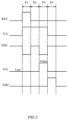
- FIG. 3 shows a schematic block diagram of a pixel circuitry according to another embodiment of the present disclosure
- FIG. 4 shows an exemplary circuit diagram of a pixel circuitry according to another embodiment of the present disclosure:
- FIG. 5 shows a timing chart of signals in a pixel circuitry according to an embodiment of the present disclosure:
- FIG. 6 A is an equivalent circuit diagram of the pixel circuitry shown in FIG. 2 in an initialization phase:
- FIG. 6 B is an equivalent circuit diagram of the pixel circuitry shown in FIG. 2 in a compensation phase:
- FIG. 6 C is an equivalent circuit diagram of the pixel circuitry shown in FIG. 2 in a data write phase:
- FIG. 6 D is an equivalent circuit diagram of the pixel circuitry shown in FIG. 2 in a light emission phase:
- FIG. 7 shows a timing chart of signals in a pixel circuitry according to another embodiment of the present disclosure:
- FIG. 8 A is an equivalent circuit diagram of the pixel circuitry shown in FIG. 4 in an initialization phase:
- FIG. 8 B is an equivalent circuit diagram of the pixel circuitry shown in FIG. 4 in a compensation phase:
- FIG. 8 C is an equivalent circuit diagram of the pixel circuitry shown in FIG. 4 in a data write phase:
- FIG. 8 D is an equivalent circuit diagram of the pixel circuitry shown in FIG. 4 in a light emission phase:
- FIG. 9 shows a flowchart of a method for driving a pixel circuitry according to an embodiment of the present disclosure:
- FIG. 10 shows a flowchart of a method for driving a pixel circuitry according to another embodiment of the present disclosure:
- connection or “coupling” are not limited to physical or mechanical connection, but can include electrical connection, direct connection or indirect connection.
- the terms “above”, “below”, “left”, “right”, or the like are only used to represent the relative position relationship. When the absolute position of the described object changes, the relative position relationship may also change accordingly.
- An OLED display device usually includes a plurality of pixel units arranged in an array. Each pixel unit can realize basic functions of driving OLED to emit light via a pixel circuitry.
- current between a source and a drain of a drive transistor can be controlled by changing a voltage of a gate of the drive transistor that directly drives the OLED to emit light, thereby achieving the change of brightness of the light emitted.
- threshold voltages of different drive transistors may be different due to process deviation. The threshold voltage of the drive transistor may drift with elapse of working time and change of working environment.
- each pixel unit may also lead to different voltage drops (I-R Drop) of the power supply, which may affect the currents driving the OLEDs.
- I-R Drop voltage drops
- the drive currents may be affected.
- Embodiments of the present disclosure provides a pixel circuitry, a driving method thereof, an array substrate and a display panel.
- deviation and drift of threshold voltage of drive transistor can be compensated.
- Brightness difference between OLEDs at a far position and a near position to a power supply caused by IR Drop can be compensated.
- Influence of capacitance of the OLED itself can be avoided. Wrong light emission of OLED can be prevented.
- display quality of the display panel comprising the pixel circuitry can be improved.
- FIG. 1 shows a schematic block diagram of a pixel circuitry according to an embodiment of the present disclosure.
- the pixel circuitry 100 may include a drive circuit 110 , a data write circuit 120 , an initialization circuit 130 , a first light emission control circuit 140 , a first storage circuit 150 , a second storage circuit 160 , and a second light emission control circuit 170 .
- the pixel circuitry 100 may be used to drive a light emitting device 200 in a corresponding pixel unit to emit light.
- a control end of the drive circuit 110 may be coupled to a first node N 1 , a first end of the drive circuit 110 may be coupled to a second node N 2 , and a second end of the drive circuit 110 may be coupled to a third node N 3 .
- the drive circuit 110 may provide a drive current I DS to the light emitting device 200 .
- the drive circuit 110 may provide a drive current I DS for driving the light emitting device 200 to emit light according to a voltage difference between the control end and the first end (that is, the voltage difference between the first node N 1 and the second node N 2 ).
- the data write circuit 120 can receive a drive signal via a drive signal terminal GA, and receive a data signal or a reference signal via a data signal terminal DA.
- the data write circuit 120 can also be coupled to the first node N 1 , and then to the control end of the drive circuit 110 .
- the data write circuit 120 can provide the data signal or reference signal from the data signal terminal DA to the first node N 1 , that is, the control end of the drive circuit 110 , according to the drive signal from the drive signal terminal GA.
- the drive signal terminal GA can be connected with a gate line corresponding to the pixel unit, such that the drive signal can be a scanning signal for the pixel unit.
- the data signal terminal DA can be connected with a data line corresponding to the pixel unit. The data line can provide a data signal or a reference signal in different time periods accordingly.
- the data write circuit 120 can be directly connected with the first node N 1 to directly provide the required signal to the N 1 node, as shown in FIG. 1 .
- the data write circuit 120 can also be indirectly connected with the first node N 1 to indirectly provide the required signal to the N 1 node, as will be described in detail below in connection with FIG. 3 .
- the initialization circuit 130 may receive a reset signal via a reset signal terminal RST and an initialization signal via an initialization signal terminal VIN 1 .
- the initialization circuit 130 may also be coupled to the second node N 2 , and thus to the first end of the drive circuit 110 .
- the initialization circuit 130 can provide the initialization signal from the initialization signal terminal VIN 1 to the second node N 2 , that is, the first end of the drive circuit 110 , according to the reset signal from the reset signal terminal RST.
- the first light emission control circuit 140 may receive a first light emission control signal via a first light emission control signal terminal EM 1 , and receive a first voltage signal via a first voltage signal terminal VDD.
- the first light emission control circuit 140 can also be coupled to the third node N 3 , and then to the second end of the drive circuit 110 .
- the first light emission control circuit 140 can provide the first voltage signal from the first voltage signal terminal VDD to the third node N 3 , that is, the second terminal of the drive circuit 110 , according to the first light emission control signal from the first light emission control signal terminal EM 1 .
- the first storage circuit 150 can be coupled with the first voltage signal terminal VDD and the second node N 2 to store a voltage difference between the first voltage signal terminal VDD and the second node N 2 .
- the second storage circuit 160 may be coupled with the first node N 1 and the second node N 2 to store a voltage difference between the first node N 1 and the second node N 2 .
- the second light emission control circuit 170 may receive a second light emission control signal via a second light emission control signal terminal EM 2 .
- the second light emission control circuit 170 can also be coupled to the second node N 2 , thereby coupling with the first end of the drive circuit 110 .
- the second light emission control circuit 170 may be coupled to the light emitting device 200 .
- the second light emission control circuit 170 can control to provide the drive current I DS to the light emitting device 200 according to the second light emission control signal from the second light emission control signal terminal EM 2 .
- the second light emission control circuit 170 can control the connection/disconnection between the drive circuit 110 and the light emitting device 200 according to the second light emission control signal, thereby preventing the light emitting device 200 from emitting light by mistake, and effectively isolating effect of capacitance of the light emitting device 200 itself on the drive current I DS .
- an end of the light emitting device 200 can be coupled with the second light emission control circuit 170 , and the other end can be coupled with a second voltage signal terminal VSS to receive a second voltage signal.
- the light emitting device 200 can emit light according to the drive current I DS provided by the drive circuit 110 under the control of the first light emission control circuit 140 and the second light emission control circuit 170 .
- the drive current I DS in the drive circuit 110 is only related to the data signal and reference signal from the data signal terminal DA. Specific analysis will be described below. As the drive current I DS is independent from characteristics of elements in the drive circuit 110 and a power supply voltage (for example, the first voltage signal, the second voltage signal), brightness uniformity of the display can be improved. Moreover, the second light emission control circuit 170 can separate the drive circuit 110 from the light emitting device 200 in a non-luminous (non-light emission) phase, thereby preventing the light emitting device 200 from emitting light by mistake, and avoiding the effect of the capacitance of the light emitting device 200 itself on the drive current I DS .
- a power supply voltage for example, the first voltage signal, the second voltage signal
- the first voltage signal terminal VDD maintains to provide a direct-current (DC) high voltage level signal, which is referred to a first voltage.
- the second voltage signal terminal VSS maintains to provide a DC low voltage level signal.
- the DC low voltage level can be referred to as the second voltage, which is lower than the first voltage.
- the initialization signal terminal VIN 1 maintains to provide a DC low voltage level signal. Similar configuration can be implemented in the following embodiments, thus repeated descriptions will be omitted.
- the first node N 1 , the second node N 2 , the third node N 3 and a fourth node N 4 may not represent actual components, but represent junction points of the related circuits in the circuit diagram. Similar configuration can be implemented in the following embodiments, thus repeated descriptions will be omitted.
- FIG. 2 shows an exemplary circuit diagram of a pixel circuitry according to an embodiment of the present disclosure, in which the pixel circuitry may be, for example, the pixel circuitry 100 of FIG. 1 .
- the pixel circuitry may include a drive transistor DT, a first transistor T 1 , a second transistor T 2 , a third transistor T 3 , a fourth transistor T 4 (for example, T 1 -T 4 may be switching transistors), a first capacitor C 1 , and a second capacitor C 2 .
- the transistors may be described as N-type field effect transistors (NMOS) as an example.
- NMOS N-type field effect transistors
- the N-type transistor can be turned on in response to a high voltage level signal of the control electrode.
- the drive circuit 110 may include a drive transistor DT.
- a control electrode of the drive transistor DT can be used as the control terminal of the drive circuit 110 and can be coupled to the first node N 1 .
- a first electrode of the drive transistor DT, as the first end of the drive circuit 110 can be coupled to the second node N 2 .
- a second electrode of the drive transistor DT, as the second end of the drive circuit 110 can be coupled to the third node N 3 .
- the drive transistor DT may be an N-type transistor.
- the data write circuit 120 may include a first transistor T 1 .
- a control electrode of the first transistor T 1 may be coupled to the drive signal terminal GA to receive the drive signal.
- a first electrode of the first transistor T 1 may be coupled to the data signal terminal DA to receive the data signal or reference signal.
- a second electrode of the first transistor T 1 may be coupled to the first node N 1 (the control electrode of the drive transistor DT).
- the first transistor T 1 may be an N-type transistor.
- the initialization circuit 130 may include a second transistor T 2 .
- a control electrode of the second transistor T 2 may be coupled to the reset signal terminal RST to receive the reset signal.
- a first electrode of the second transistor T 2 may be coupled to the initialization signal terminal VIN 1 to receive the initialization signal.
- a second electrode of the second transistor T 2 may be coupled to second node N 2 (the first electrode of the drive transistor DT).
- the second transistor T 2 may be an N-type transistor.
- the first light emission control circuit 140 may include a third transistor T 3 .
- a control electrode of the third transistor T 3 may be coupled to the first light emission control signal terminal EM 1 to receive the first light emission control signal.
- a first electrode of the third transistor T 3 may be coupled to the first voltage signal terminal VDD to receive the first voltage signal.
- a second electrode of the third transistor T 3 may be coupled to the third node N 3 (the second electrode of the drive transistor DT).
- the third transistor T 3 may be an N-type transistor.
- the first storage circuit 150 may include a first capacitor C 1 .
- a first end of the first capacitor C 1 may be coupled to the first voltage signal terminal VDD, and a second end of the first capacitor C 1 may be coupled to the second node N 2 .
- the second storage circuit 160 may include a second capacitor C 2 .
- a first end of the second capacitor C 2 may be coupled to the first node N 1
- a second end of the second capacitor C 2 may be coupled to the second node N 2 .
- the second light emission control circuit 170 may include a fourth transistor T 4 .
- a control electrode of the fourth transistor T 4 may be coupled to the second light emission control signal terminal EM 2 to receive the light emission control signal.
- a first electrode of the fourth transistor T 4 may be coupled to the second node N 2 .
- a second electrode of the fourth transistor T 4 may be coupled to the light emitting device 200 .
- the fourth transistor T 4 may be an N-type transistor.
- one or more of the drive circuit 110 , the data write circuit 120 , the initialization circuit 130 , the first light emission control circuit 140 , the first storage circuit 150 , the second storage circuit 160 , and the second light emission control circuit 170 may also be circuits with other elements, and are not limited to the above description.
- the light emitting device 200 may be an OLED, such as in various types, e.g., top emitting, bottom emitting, bilateral emitting, or the like, and can emit red light, green light, blue light, white light, or the like.
- the OLED type are not limited to the above.
- an anode of the OLED may be coupled to the second electrode of the fourth transistor T 4
- a cathode of the OLED may be coupled to the second voltage signal terminal VSS to receive the second voltage signal.
- FIG. 2 also schematically shows a capacitor Coled of the OLED, which may be in parallel with both ends of the OLED.
- the data signal terminal may provide the data signal and the reference signal in different time periods.
- the reference signal can also be provided separately in other ways without transmitting the reference signal via the data signal terminal. Therefore, the data signal terminal can only transmit the data signal, thus simplifying the design of the drive circuit. For details, reference can be made to the description of the following embodiments.
- a third storage circuit 310 may be additionally provided between the drive circuit 110 and the data write circuit 120 .
- an end of the third storage circuit 310 may be coupled to the control end of the drive circuit 110 via the first node N 1 .
- the other end of the third storage circuit 310 may be coupled to the data write circuit 120 via the fourth node N 4 .
- the data write circuit 120 can provide the data signal from the data signal terminal DA to the fourth node N 4 according to the drive signal from the drive signal terminal GA.
- the third storage circuit 310 may store a voltage difference between the fourth node N 4 and the first node N 1 .
- the first reference circuit 320 may receive a reset signal via the reset signal terminal RST, and receive a first reference signal via the first reference signal terminal REF 1 .
- the first reference circuit 320 may also be coupled to the first node N 1 .
- the first reference circuit 320 can provide the first reference signal from the first reference signal terminal REF 1 to the first node N 1 , according to the reset signal from the reset signal terminal RST, to control a voltage of the first node N 1 .
- the second reference circuit 330 may receive a reset signal via the reset signal terminal RST, and receive a second reference signal via the second reference signal terminal REF 2 .
- the second reference circuit 330 may also be coupled to the fourth node N 4 .
- the second reference circuit 330 can provide the second reference signal from the second reference signal terminal REF 2 to the fourth node N 4 , according to the reset signal from the reset signal terminal RST, to control a voltage of the fourth node N 4 .
- first reference signal and the second reference signal may be same signals, such as same low voltage level signal. In another embodiment, the first reference signal and the second reference signal may also be different signals.
- FIG. 4 shows an exemplary circuit diagram of a pixel circuitry according to an embodiment of the present disclosure, in which, for example, the pixel circuitry may be the pixel circuitry in FIG. 3 .
- the pixel circuitry may include a drive transistor DT, a first transistor T 1 , a second transistor T 2 , a third transistor T 3 , a fourth transistor T 4 , a fifth transistor (for example, T 1 -T 5 may be switching transistors), a first capacitor C 1 , a second capacitor C 2 , and a third capacitor C 3 . Except for the third capacitor C 3 , the fifth transistor T 5 and the sixth transistor T 6 , each element in the pixel circuitry in FIG.
- the structure and function of the light emitting device in FIG. 4 may be the same as the structure and function of the light emitting device in FIG. 2 .
- the transistors adopted can be N-type transistor or P-type transistor.
- the transistor can be an N-type or P-type field effect transistor (MOSFET), or an N-type or P-type bipolar transistor (BJT).
- a gate of the transistor can be referred to as a control electrode.
- the source and drain of a transistor are symmetrical, the source and drain may not be distinguished. That is, the source of a transistor can be a first electrode (or a second electrode), and the drain can be the second electrode (or the first electrode).
- the transistors may be described as N-type field effect transistors (NMOS) as an example.
- NMOS N-type field effect transistors
- the N-type transistor may be turned on in response to a high voltage level signal of the control electrode.
- the third storage circuit 310 may include a third capacitor C 3 .
- a first end of the third capacitor C 3 may be coupled to the fourth node N 4
- a second end of the third capacitor C 3 may be coupled to the first node N 1 .
- the first reference circuit 320 may include a fifth transistor T 5 .
- a control electrode of the fifth transistor T 5 may be coupled to the reset signal terminal RST to receive the reset signal.
- a first electrode of the fifth transistor T 5 may be coupled to the first reference signal terminal REF 1 to receive the first reference signal REF 1 .
- a second electrode of the fifth transistor T 5 may be coupled to the first node N 1 .
- the fifth transistor T 5 may be an N-type transistor.
- the second reference circuit 330 may include a sixth transistor T 6 .
- a control electrode of the sixth transistor T 6 may be coupled to the reset signal terminal RST to receive the reset signal.
- a first electrode of the sixth transistor T 6 may be coupled to the second reference signal terminal REF 2 to receive the second reference signal REF 2 .
- a second electrode of the sixth transistor T 6 may be coupled to the fourth node N 4 .
- the sixth transistor T 6 may be an N-type transistor.
- the third storage circuit 310 may also be circuits with other elements, and are not limited to those described above.
- FIG. 5 shows a timing chart of signals for driving a pixel circuitry of an embodiment of the present disclosure.
- the pixel circuitry may be, for example, the pixel circuitry shown in FIG. 2 .
- the working process of the pixel circuitry may include four phases, such as, an initial phase P 1 , a compensation phase P 2 , a data write phase P 3 and a light emission phase P 4 .
- FIG. 6 A is an equivalent circuit diagram of the pixel circuitry shown in FIG. 2 at the initialization phase.
- FIG. 6 B is an equivalent circuit diagram of the pixel circuitry shown in FIG. 2 in the compensation phase.
- FIG. 6 C is an equivalent circuit diagram of the pixel circuitry shown in FIG. 2 in the data write phase.
- FIG. 6 D is an equivalent circuit diagram of the pixel circuitry shown in FIG. 2 in the light emission phase.
- symbols VDD. VSS and VIN 1 may be used to represent both corresponding voltage signal terminal and the corresponding voltage.
- the first voltage signal terminal VDD may provide a high voltage level signal
- the second voltage signal terminal VSS may provide a low voltage level signal
- the initialization signal terminal VIN 1 may provide a low voltage level signal.
- symbols RST, GA, EM 1 and EM 2 may be used to represent both corresponding signal terminals and corresponding signals.
- a symbol Vref may represent both the reference signal at the data signal terminal DA and the corresponding voltage.
- a symbol Vdata may represent both the data signal at the data signal terminal DA and the corresponding voltage.
- the transistor identified with a symbol “x” indicates that the transistor is in a turned-off state in the corresponding phase.
- FIG. 6 A Taking the first transistor T 1 , the second transistor T 2 , the third transistor T 3 , the fourth transistor T 4 and the drive transistor DT being N-type transistors as an example, the following describes a working process of the pixel circuitry in FIG. 2 in combination with FIG. 5 .
- FIG. 6 A FIG. 6 B .
- FIG. 6 C and FIG. 6 D Taking the first transistor T 1 , the second transistor T 2 , the third transistor T 3 , the fourth transistor T 4 and the drive transistor DT being N-type transistors as an example, the following describes a working process of the pixel circuitry in FIG. 2 in combination with FIG. 5 .
- FIG. 6 A FIG. 6 B .
- FIG. 6 C and FIG. 6 D Taking the first transistor T 1 , the second transistor T 2 , the third transistor T 3 , the fourth transistor T 4 and the drive transistor DT being N-type transistors as an example, the following describes a working process of the pixel circuitry in FIG. 2 in combination with FIG.
- the drive signal GA and the reset signal RST may be provided at a high voltage level.
- the first light emission control signal EM 1 and the second light emission control signal EM 2 may be provided at a low voltage level.
- the data signal terminal DA may provide a reference signal Vref, such as at a low voltage level.
- the first transistor T 1 in the initialization phase P 1 , can be turned on, under the control of the drive signal GA at the high voltage level, to provide the reference signal Vref from the data signal terminal DA to the first node N 1 .
- a voltage V N1 of the first node N 1 (that is, the control electrode of the drive transistor) can be initialized to the voltage Vref.
- the second transistor T 2 can be turned on, under the control of the reset signal RST at the high voltage level, to provide the low voltage level initialization signal VIN 1 to the second node N 2 .
- a voltage V N2 of the second node N 2 (that is, the first electrode of the drive transistor) can be initialized to the voltage VIN 1 .
- the third transistor T 3 can be turned off, under the control of the first light emission control signal EM 1 at the low voltage level, to separate the first voltage signal terminal VDD from the drive transistor DT.
- the fourth transistor T 4 can be turned off, under the control of the second light emission control signal EM 2 at the low voltage level, to separate the drive transistor DT from the OLED.
- the drive current I DS of the drive transistor DT could not be transferred to the OLED, avoiding the OLED from emitting light by mistake.
- the drive signal GA and the first light emission control signal EM 1 may be provided at a high voltage level.
- the reset signal RST and the second light emission control signal EM 2 may be provided at a low voltage level.
- the data signal terminal DA may provide the reference signal Vref, such as at a low voltage level.
- the first transistor T 1 in the compensation phase P 2 , can be turned on, under the control of the drive signal GA at the high voltage level, to provide the reference signal Vref from the data signal terminal DA to the first node N 1 . Therefore, the voltage V N1 of the first node N 1 can be maintained as Vref.
- the third transistor T 3 can be turned on, under the control of the first light emission control signal EM 1 at the high voltage level, to provide the first voltage signal VDD to the third node N 3 . In this case, the drive transistor DT can be turned on.
- the drive current I DS of the drive transistor DT can charge the second node N 2 , to increase the voltage V N2 of the second node N 2 until the voltage V N2 reaches Vref-Vth.
- Vth is the threshold voltage of drive transistor DT.
- the first capacitor C 1 can store the voltage difference between the first voltage signal terminal VDD and the second node N 2 .
- the second capacitor C 2 can store the voltage difference between the first node N 1 and the second node N 2 .
- the fourth transistor T 4 can be turned off, under the control of the second light emission control signal EM 2 at low voltage level, to disconnect a path between the drive transistor DT and the OLED.
- the drive current I DS could not be transferred to the OLED, thus avoiding the OLED from emitting light by mistake.
- the second transistor T 2 can be turned off, under the control of the reset signal RST at the low voltage level.
- the drive signal GA may be provided at a high voltage level.
- the reset signal RST, the first light emission control signal EM 1 and the second light emission control signal EM 2 may be provided at a low voltage level.
- the data signal terminal DA may provide a data signal Vdata.
- the first transistor T 1 in the data write phase P 3 , can be turned on, under the control of the drive signal at the high voltage level, to provide the data signal Vdata from the data signal terminal to the first node N 1 .
- the voltage V N1 of the first node N 1 can be Vdata.
- the second transistor T 2 can be turned off, under the control of the reset signal RST at the low voltage level.
- the third transistor T 3 can be turned off, under the control of the first light emission control signal EM 1 at the low voltage level.
- the fourth transistor T 4 can be turned off, under the control of the second light emission control signal EM 2 at the low voltage level.
- the first capacitor C 1 can store the voltage difference between the first voltage signal terminal VDD and the second node N 2 .
- the second capacitor C 2 can store the voltage difference between the first node N 1 and the second node N 2 . Therefore, as the voltage V N1 of the first node N 1 changes, the voltage V N2 of the second node N 2 may also change accordingly.
- the voltage V N2 of the second node N 2 can be calculated as: Vref ⁇ Vth +( C 2/( C 2+ C 1))*(Vdata ⁇ Vref).
- the drive current I DS could not be transferred to the OLED, thereby preventing the OLED from emitting light by mistake. Meanwhile, it can also avoid the effect of the capacitance of OLED itself on the drive current I DS .
- the first light emission control signal and the second light emission control signal may be provided at a high voltage level.
- the drive signal GA and the reset signal RST may be provided at a low voltage level.
- the third transistor T 3 can be turned on, under the control of the first light emission control signal EM 1 at the high voltage level, to connect the first voltage signal terminal VDD with the drive transistor DT.
- the fourth transistor T 4 can be turned on, under the control of the second light emission control signal EM 2 at the high voltage level, to connect the drive transistor DT with the OLED.
- the first transistor T 1 can be turned off, under the control of the drive signal GA at the low voltage level.
- the second transistor T 2 can be turned off, under the control of the reset signal RST at the low voltage level.
- the first capacitor C 1 can maintain the voltage difference between the first voltage signal terminal VDD and the second node N 2 .
- the second capacitor C 2 can maintain the voltage difference between the first node N 1 and the second node N 2 . Therefore, the voltages of the first node N 1 and the second node N 2 can be the same as those in the previous phase.
- the drive current I DS of the drive transistor DT can be provided to the OLED such that the OLED can emit light.
- the drive current I DS can be calculated according to the following equations:
- I D ⁇ S 1 2 ⁇ ⁇ ⁇ C o ⁇ x ⁇ W L ⁇ ( V gs - V th ) 2
- V gs V th + ( V data - V ref ) ⁇ C 1 C 1 + C 2
- ⁇ , C ox , W, and L are constant values related to the drive transistor DT, where ⁇ is an electron mobility of the drive transistor DT, C ox is an oxide capacitance per unit area of the drive transistor DT, W is a channel width of the drive transistor DT, and L is a channel length of the drive transistor DT.
- Vgs may represent a voltage between the gate (or control electrode) and the source (or first electrode) of the drive transistor DT.
- Vth may represent the threshold voltage of the drive transistor DT.
- the drive current flowing through the light emitting device OLED may no longer be related to the threshold voltage of the drive transistor DT, the power supply voltage (for example, the first voltage VDD, the second voltage VSS), or the capacitance Coled of the light emitting device itself.
- the compensation of the pixel circuitry can be realized.
- the problem of the drift of the threshold voltage caused by the manufacturing process and long-time working process of the drive transistor DT can be solved.
- the problem of different power supply voltages provided to each pixel circuitry due to different positions of each pixel unit can be solved.
- the problem of different capacitance Coled of each light emitting device can be solved, thereby eliminating the impact on the drive current. Therefore, the display effect of the display device with the pixel circuitry can be improved.
- FIG. 7 shows a timing chart of signals for driving a pixel circuitry of an embodiment of the present disclosure.
- the pixel circuitry is, for example, the pixel circuitry shown in FIG. 4 .
- the working process of the pixel circuitry may include four phases, such as, an initial phase P 1 , a compensation phase P 2 , a data write phase P 3 and a light emission phase P 4 .
- FIG. 8 A is an equivalent circuit diagram of the pixel circuitry shown in FIG. 4 in the initialization phase.
- FIG. 8 B is an equivalent circuit diagram of the pixel circuitry shown in FIG. 4 in the compensation phase.
- FIG. 8 C is an equivalent circuit diagram of the pixel circuitry shown in FIG. 4 in the data write phase.
- FIG. 8 D is an equivalent circuit diagram of the pixel circuitry shown in FIG. 4 in the light emission phase.
- the symbols VDD. VSS and VIN 1 may be used to represent both the corresponding voltage signal terminal and the corresponding voltage.
- the first voltage signal terminal VDD may provide a high voltage level signal
- the second voltage signal terminal VSS may provide a low voltage level signal
- the initialization signal terminal VIN 1 may provide a low voltage level signal.
- symbols RST, GA, EM 1 and EM 2 may be used to represent both corresponding signal terminals and corresponding signals.
- a symbol Vdata may represent both a data signal at the data signal terminal DA and the corresponding voltage.
- a symbol Vref 1 may represent both a first reference signal at the first reference signal terminal REF 1 and the corresponding voltage.
- a symbol Vref 2 may represent a second reference signal at the second reference signal terminal REF 2 and the corresponding voltage.
- the transistor identified with “x” indicates that the transistor is in a turned-off state in the corresponding phase.
- FIG. 4 Taking the first transistor T 1 , the second transistor T 2 , the third transistor T 3 , the fourth transistor T 4 , the fifth transistor T 5 , the sixth transistor T 6 and the drive transistor DT being N-type transistors as an example, the working process of the pixel circuitry in FIG. 4 can be described in combination with FIG. 7 .
- FIG. 8 C and FIG. 8 D the working process of the pixel circuitry in FIG. 4 can be described in combination with FIG. 7 .
- FIG. 8 C and FIG. 8 D the working process of the pixel circuitry in FIG. 4 can be described in combination with FIG. 7 .
- the reset signal RST may be provided at a high voltage level.
- the drive signal GA, the first light emission control signal EM 1 , and the second light emission control signal EM 2 may be provided at a low voltage level.
- FIG. 7 shows the signal at the data signal terminal DA as an example, it can be understood that the data signal terminal can provide a data signal or any appropriate signal, which is not limited. Embodiments will be described below.
- the first transistor T 1 can be turned off under the control of the drive signal GA at the low voltage level, thus separating the data signal terminal DA from the fourth node N 4 .
- the signal at the data signal terminal DA is not be transmitted to the fourth node N 4 , there is no need to limit the signal at the data signal terminal DA. That is, the data signal terminal DA may not need to transmit a reference signal, which can be a data signal or any other signal.
- the third transistor T 3 can be turned off, under the control of the first light emission control signal EM 1 at the low voltage level to separate the first voltage signal terminal VDD from the drive transistor DT.
- the fourth transistor T 4 can be turned off, under the control of the second light emission control signal EM 2 at the low voltage level, to separate the drive transistor DT from the OLED.
- the drive current I DS of the drive transistor DT could not be transferred to the OLED, avoiding the OLED from emitting light by mistake.
- the first light emission control signal EM 1 may be provided at a high voltage level.
- the drive signal GA, the reset signal RST, and the second light emission control signal EM 2 may be provided at a low voltage level.
- the data signal terminal DA can provide data signal or any signal, which is not limited herein.
- the first transistor T 1 can be turned off, under the control of the drive signal GA at the low voltage level, such that the signal at the data signal terminal DA is not transmitted to the fourth node N 4 .
- the signal at the data signal terminal DA can be the data signal or any signal.
- the fifth transistor T 5 and the sixth transistor T 6 can be turned off, under the control of the reset signal RST at the low voltage level.
- the third capacitor can store the voltage difference between the fourth node N 4 and the first node N 1
- the first node N 1 and the fourth node N 4 can respectively maintain the corresponding voltage in the previous phase. That is, the voltage V N1 of the first node N 1 is Vref 1 , and the voltage V N4 of the fourth node N 4 is Vref 2 .
- the third transistor T 3 can be turned on, under the control of the first light emission control signal EM 1 at the high voltage level, to provide the first voltage signal VDD to the third node N 3 .
- the first capacitor C 1 can store the voltage difference between the first voltage signal terminal VDD and the second node N 2 .
- the second capacitor C 2 can store the voltage difference between the first node N 1 and the second node N 2 .
- the drive transistor DT can be turned on.
- the drive current I DS of the drive transistor DT can charge the second node N 2 to increase the voltage V N2 of the second node N 2 until the voltage V N2 reaches Vref 1 -Vth.
- Vth is the threshold voltage of drive transistor DT.
- the fourth transistor T 4 can be turned off, under the control of the second light emission control signal EM 2 at the low voltage level, to disconnect a path between the drive transistor DT and the light emitting device 200 .
- the drive current I DS may not be transferred to the OLED, avoiding the OLED from emitting light by mistake.
- the second transistor T 2 can be turned off, under the control of the reset signal RST at the low voltage level.
- the drive signal GA may be provided at a high voltage level.
- the reset signal RST, a first light emission control signal EM 1 and a second light emission control signal EM 2 may be provided at a low voltage level.
- the data signal terminal DA may provide a data signal Vdata.
- the first transistor T 1 can be turned on, under the control of the drive signal GA at the high voltage level, to provide the data signal Vdata from the data signal terminal DA to the fourth node N 4 , such that the voltage V N4 of the fourth node N 4 can be Vdata.
- the first capacitor C 1 can store the voltage difference between the first voltage signal terminal VDD and the second node N 2 .
- the second capacitor C 2 can store the voltage difference between the first node N 1 and the second node N 2
- the third capacitor can store the voltage difference between the fourth node N 4 and the first node N 1 . Therefore, as the voltage VN 4 of the fourth node N 4 changes, the voltage VN 1 of the first node N 1 and the voltage VN 2 of the second node N 2 can also change accordingly.
- the voltages of the first node N 1 and the second node N 2 can be calculated as:
- V N ⁇ 1 ( V data - V ref ⁇ 2 ) ⁇ ( C 3 * C 2 + C 3 * C 1 ) ( C 3 * C 2 + C 1 * C 2 + C 3 * C 1 ) + V ref ⁇ 1
- V N ⁇ 2 ( V data - V ref ⁇ 2 ) ⁇ ( C 3 * C 2 ) ( C 3 * C 2 + C 1 * C 2 + C 3 * C 1 ) + V ref ⁇ 1 - V th .
- the drive current I DS may not be transferred to the OLED, preventing the OLED from emitting light by mistake. Meanwhile, it can also avoid the effect of the capacitance of OLED itself on the drive current I DS .
- the first light emission control signal EM 1 and the second light emission control signal EM 2 may be provided at a high voltage level.
- the drive signal GA and a reset signal RST can be provided at a low voltage level.
- the data signal terminal DA can provide data signal or any signal, which is not limited herein.
- the third transistor T 3 can be turned on, under the control of the first light emission control signal EM 1 at the high voltage level, to connect the first voltage signal terminal VDD with the drive transistor DT.
- the fourth transistor T 4 can be turned on, under the control of the second light emission control signal EM 2 at the high voltage level, to connect the drive transistor DT with the OLED.
- the first transistor T 1 can be turned off, under the control of the drive signal GA at the low voltage level.
- the second transistor T 2 , the fifth transistor T 5 , and the sixth transistor T 6 can be turned off, under the control of the reset signal RST at the low voltage level.
- the first capacitor C 1 can maintain the voltage difference between the first voltage signal terminal VDD and the second node N 2 .
- the second capacitor C 2 can maintain the voltage difference between the first node N 1 and the second node N 2 .
- the third capacitor can store the voltage difference between the fourth node N 4 and the first node N 1 . Therefore, the voltage V N1 of the first node N 1 , the voltage V N2 of the second node N 2 , and the voltage V N4 of the fourth node N 4 can be stored via the capacitors, and can be the same as those in the previous phase.
- the drive current I DS of the drive transistor DT can be provided to the OLED, such that the OLED can emit light.
- the drive current I DS can be calculated according to the following equations:
- ⁇ , C ox , W, and L are constant values related to the drive transistor DT, where ⁇ is an electron mobility of the drive transistor DT, C ox is an oxide capacitance per unit area of the drive transistor DT, W is a channel width of the drive transistor DT, and L is a channel length of the drive transistor DT.
- Vgs may represent a voltage between the gate (or control electrode) and the source (or first electrode) of the drive transistor DT.
- Vth may represent the threshold voltage of the drive transistor DT.
- the drive current flowing through the light emitting device OLED may no longer be related to the threshold voltage of the drive transistor DT, the power supply voltage (for example, the first voltage VDD, the second voltage VSS), or the capacitance Coled of the light emitting device itself.
- the compensation of the pixel circuitry can be realized.
- the problem of the drift of the threshold voltage caused by the manufacturing process and long-time working process of the drive transistor DT can be solved.
- the problem of different power supply voltages provided to each pixel circuitry due to different positions of each pixel unit can be solved.
- the problem of different capacitance Coled of each light emitting device can be solved, thereby eliminating the impact on the drive current. Therefore, the display effect of the display device with the pixel circuitry can be improved.
- the data signal terminal can only transmit the data signal but not transmitting other reference signal, thereby simplifying the design of the drive circuit.
- first reference signal Vref 1 and the second reference signal Vref 2 may be the same signal. In other examples, the first reference signal Vref 1 and the second reference signal Vref 2 may also be different signals.
- FIG. 9 shows a schematic flowchart of a method for driving a pixel circuitry according to an embodiment of the present invention.
- the pixel circuitry may be, for example, the pixel circuitry shown in FIG. 1 , and may adopt the circuit structure of the pixel circuitry shown in FIG. 2 , for example.
- step S 910 in the initialization phase, the drive signal and the reset signal can be provided to turn on the data write circuit and the initialization circuit.
- the reference signal from the data signal terminal can be provided to the first node via the data write circuit.
- the initialization signal can be provided to the second node via the initialization circuit.
- step S 920 in the compensation phase, the drive signal and the first light emission control signal can be provided to turn on the data write circuit and the first light emission control circuit.
- the reference signal can be provided to the first node via the data write circuit.
- the first voltage signal can be provided to the third node via the first light emission control circuit.
- the first storage circuit and the second storage circuit can be charged to compensate the drive circuit.
- step S 930 in the data write phase, the drive signal can be provided to turn on the data write circuit, to provide the data signal from the data signal terminal to the first node.
- step S 940 in the light emission phase, the first light emission control signal and the second light emission control signal can be provided, to turn on the first light emission control circuit and the second light emission control circuit.
- the drive current of the drive circuit can be provided to the light emitting device, such that the light emitting device can emit light.
- the driving method shown in FIG. 9 can be implemented with the timing chart of the signals in the pixel circuitry shown in FIG. 5 and the above related description.
- FIG. 10 shows a schematic flowchart of a method for driving a pixel circuitry according to an embodiment of the present invention.
- the pixel circuitry may be, for example, the pixel circuitry shown in FIG. 3 , and may adopt the circuit structure of the pixel circuitry shown in FIG. 4 , for example.
- the reset signal in step S 1010 , in the initialization phase, can be provided to turn on the initialization circuit, the first reference circuit and the second reference circuit.
- the initialization signal can be provided to the second node via the initialization circuit.
- the first reference signal can be provided to the first node via the first reference circuit.
- the second reference signal can be provided to the fourth node via the second reference circuit.
- the first light emission control signal in the compensation phase, can be provided to turn on the first light emission control circuit.
- the first voltage signal can be provided to the third node via the first light emission control circuit.
- the first storage circuit, the second storage circuit, and the third storage circuit can be charged to compensate the drive circuit.
- step S 1030 in the data write phase, the drive signal can be provided to turn on the data write circuit, to provide the data signal from the data signal terminal to the fourth node.
- step S 1040 in the light emission phase, the first light emission control signal and the second light emission control signal can be provided to turn on the first light emission control circuit and the second light emission control circuit.
- the drive current of the drive circuit can be provided to the light emitting device, such that the light emitting device can emit light.
- the driving method shown in FIG. 10 can be implemented with the timing chart of the signals in the pixel circuitry shown in FIG. 7 and the above related description.
- FIG. 11 shows a schematic diagram of an array substrate according to an embodiment of the present disclosure.
- the array substrate 1100 may include a plurality of pixel circuitries, for example, the pixel circuitry according to an embodiment of the present disclosure.
- the plurality of pixel circuitries e, g., pixel circuitries 1011 , 1012 , 1021 , 1022 , etc.
- the plurality of pixel circuitries may be set in a matrix form.
- embodiments of the present disclosure may also provide a display panel including the above array substrate.
- Embodiments of the present disclosure may also provide a display device including the display panel.
- the display device may be, for example, a display screen, a mobile phone, a tablet computer, a camera, a wearable device, and the like.
- the embodiment of the present disclosure can compensate for the deviation and drift of the threshold voltage of the drive transistor in the plurality of pixel circuitries, as well as the brightness difference between the far end and the near end of the power supply caused by IR drop, thereby avoiding the effect of the capacitance of the light emitting device itself Coled on the drive current.
- the brightness uniformity and the display quality of the display can be improved.
- it can also prevent the light emission element from emitting light by mistake in the non-luminous phase.
- the data signal terminal may only transmit the data signal but not transmitting other reference signal, thus simplifying the design of the drive circuit.
Landscapes
- Engineering & Computer Science (AREA)
- Physics & Mathematics (AREA)
- Computer Hardware Design (AREA)
- General Physics & Mathematics (AREA)
- Theoretical Computer Science (AREA)
- Control Of Indicators Other Than Cathode Ray Tubes (AREA)
- Electroluminescent Light Sources (AREA)
Abstract
Description
Vref−Vth+(C2/(C2+C1))*(Vdata−Vref).
Claims (12)
Applications Claiming Priority (1)
| Application Number | Priority Date | Filing Date | Title |
|---|---|---|---|
| PCT/CN2021/075706 WO2022165782A1 (en) | 2021-02-07 | 2021-02-07 | Pixel circuit and driving method therefor, array substrate, and display panel |
Publications (2)
| Publication Number | Publication Date |
|---|---|
| US20230343287A1 US20230343287A1 (en) | 2023-10-26 |
| US12094409B2 true US12094409B2 (en) | 2024-09-17 |
Family
ID=82741899
Family Applications (1)
| Application Number | Title | Priority Date | Filing Date |
|---|---|---|---|
| US18/044,114 Active US12094409B2 (en) | 2021-02-07 | 2021-02-07 | Pixel circuitry and driving method thereof, array substrate and display panel |
Country Status (4)
| Country | Link |
|---|---|
| US (1) | US12094409B2 (en) |
| EP (1) | EP4202898B1 (en) |
| CN (1) | CN115244607A (en) |
| WO (1) | WO2022165782A1 (en) |
Families Citing this family (5)
| Publication number | Priority date | Publication date | Assignee | Title |
|---|---|---|---|---|
| CN115410531B (en) * | 2022-09-09 | 2024-09-10 | 合肥视涯显示科技有限公司 | Pixel circuit, driving method thereof, silicon-based display panel and display device |
| CN116343648B (en) * | 2023-03-22 | 2025-10-31 | 合肥维信诺科技有限公司 | Pixel driving circuit, driving method thereof and display device |
| CN118865857A (en) * | 2023-04-27 | 2024-10-29 | 京东方科技集团股份有限公司 | Pixel circuit, display device and driving method |
| WO2025091173A1 (en) * | 2023-10-30 | 2025-05-08 | 京东方科技集团股份有限公司 | Pixel circuit, pixel driving circuit and display device |
| CN121866613A (en) * | 2024-02-27 | 2026-04-14 | 京东方科技集团股份有限公司 | Pixel circuits, driving methods, and display devices |
Citations (8)
| Publication number | Priority date | Publication date | Assignee | Title |
|---|---|---|---|---|
| US20130057532A1 (en) | 2011-09-05 | 2013-03-07 | Young-Hak Lee | Pixel circuit of organic light emitting diode display device |
| US20140184665A1 (en) | 2012-12-28 | 2014-07-03 | Lg Display Co., Ltd. | Organic light emitting diode display device and method for driving the same |
| CN105825815A (en) | 2016-05-24 | 2016-08-03 | 上海天马有机发光显示技术有限公司 | Organic light-emitting pixel circuit and driving method thereof |
| US20180005576A1 (en) | 2016-06-30 | 2018-01-04 | Lg Display Co., Ltd. | Organic light emitting display device and driving method of the same |
| US20180122301A1 (en) | 2016-10-31 | 2018-05-03 | Lg Display Co., Ltd. | Organic Light Emitting Diode Display Device and Method for Driving the Same |
| CN111179820A (en) * | 2020-03-12 | 2020-05-19 | 武汉华星光电半导体显示技术有限公司 | Pixel circuit and display panel |
| CN111477178A (en) | 2020-05-26 | 2020-07-31 | 京东方科技集团股份有限公司 | A pixel driving circuit, a driving method thereof, and a display device |
| EP3723077A1 (en) | 2017-12-04 | 2020-10-14 | Boe Technology Group Co. Ltd. | Pixel circuit and drive method therefor, and display apparatus |
-
2021
- 2021-02-07 CN CN202180000171.2A patent/CN115244607A/en active Pending
- 2021-02-07 US US18/044,114 patent/US12094409B2/en active Active
- 2021-02-07 EP EP21923795.5A patent/EP4202898B1/en active Active
- 2021-02-07 WO PCT/CN2021/075706 patent/WO2022165782A1/en not_active Ceased
Patent Citations (13)
| Publication number | Priority date | Publication date | Assignee | Title |
|---|---|---|---|---|
| US20130057532A1 (en) | 2011-09-05 | 2013-03-07 | Young-Hak Lee | Pixel circuit of organic light emitting diode display device |
| US20140184665A1 (en) | 2012-12-28 | 2014-07-03 | Lg Display Co., Ltd. | Organic light emitting diode display device and method for driving the same |
| CN103915061A (en) | 2012-12-28 | 2014-07-09 | 乐金显示有限公司 | Organic light emitting diode display device and method for driving the same |
| CN105825815A (en) | 2016-05-24 | 2016-08-03 | 上海天马有机发光显示技术有限公司 | Organic light-emitting pixel circuit and driving method thereof |
| US20180005576A1 (en) | 2016-06-30 | 2018-01-04 | Lg Display Co., Ltd. | Organic light emitting display device and driving method of the same |
| CN107564476A (en) | 2016-06-30 | 2018-01-09 | 乐金显示有限公司 | Organic light-emitting display device |
| US20180122301A1 (en) | 2016-10-31 | 2018-05-03 | Lg Display Co., Ltd. | Organic Light Emitting Diode Display Device and Method for Driving the Same |
| CN108010485A (en) | 2016-10-31 | 2018-05-08 | 乐金显示有限公司 | Organic LED display device and the method for driving it |
| EP3723077A1 (en) | 2017-12-04 | 2020-10-14 | Boe Technology Group Co. Ltd. | Pixel circuit and drive method therefor, and display apparatus |
| CN111179820A (en) * | 2020-03-12 | 2020-05-19 | 武汉华星光电半导体显示技术有限公司 | Pixel circuit and display panel |
| US20220122531A1 (en) * | 2020-03-12 | 2022-04-21 | Wuhan China Star Optoelectronics Semiconductor Display Technology Co., Ltd. | Pixel circuit and display panel |
| CN111477178A (en) | 2020-05-26 | 2020-07-31 | 京东方科技集团股份有限公司 | A pixel driving circuit, a driving method thereof, and a display device |
| US20220343842A1 (en) | 2020-05-26 | 2022-10-27 | Boe Technology Group Co., Ltd. | Pixel driving circuit, method for driving the same and display device |
Non-Patent Citations (3)
| Title |
|---|
| International Search Report issued for International Application No. PCT/CN2021/075706, mailed on Oct. 28, 2021. |
| Search Report issued for European Application No. 21923795.5, mailed on Oct. 5, 2023. 13 pages. |
| Written Opinion of the International Searching Authority issued for International Application No. PCT/CN2021/075706, mailed on Oct. 28, 2021. |
Also Published As
| Publication number | Publication date |
|---|---|
| EP4202898A4 (en) | 2023-11-08 |
| EP4202898B1 (en) | 2025-06-18 |
| EP4202898A1 (en) | 2023-06-28 |
| US20230343287A1 (en) | 2023-10-26 |
| CN115244607A (en) | 2022-10-25 |
| WO2022165782A1 (en) | 2022-08-11 |
Similar Documents
| Publication | Publication Date | Title |
|---|---|---|
| US10769998B2 (en) | Pixel circuit and driving method thereof, array substrate, and display panel | |
| US12094409B2 (en) | Pixel circuitry and driving method thereof, array substrate and display panel | |
| US10991303B2 (en) | Pixel circuit and driving method thereof, display device | |
| US20200273411A1 (en) | Pixel circuit and driving method thereof, and display device | |
| CN110097848B (en) | Display device, driving method for display device, and electronic apparatus | |
| US11915646B2 (en) | Organic light-emitting diode pixel circuit and driving method therefor, and display panel and display apparatus | |
| CN109559686B (en) | Pixel circuit, driving method, electroluminescent display panel and display device | |
| US8937489B2 (en) | Inverter and scan driver using the same | |
| US20160005356A1 (en) | Oled Pixel Circuit, Driving Method of the Same, and Display Device | |
| US20160035276A1 (en) | Oled pixel circuit, driving method of the same, and display device | |
| TWI423220B (en) | Display device, method for laying wires in display device, and electronic device | |
| WO2020001026A1 (en) | Pixel driving circuit and method, and display panel | |
| US11568815B2 (en) | Pixel driving circuit, manufacturing method thereof, and display device | |
| WO2020001027A1 (en) | Pixel drive circuit and method, and display device | |
| CN104933993A (en) | Pixel driving circuit and driving method thereof and display device | |
| CN111105751A (en) | Display device, method for driving display device, and electronic device | |
| US10475385B2 (en) | AMOLED pixel driving circuit and driving method capable of ensuring uniform brightness of the organic light emitting diode and improving the display effect of the pictures | |
| CN113327556A (en) | Pixel circuit, driving method thereof and display panel | |
| US11056063B2 (en) | Pixel circuit and driving method therefor, and display device | |
| US20210210013A1 (en) | Pixel circuit and driving method, display panel, display device | |
| CN114255706A (en) | Pixel circuit with reduced sensitivity to diode-connected switch threshold variations | |
| CN110264953A (en) | Pixel circuit, driving method thereof, pixel structure and display device | |
| US10223967B1 (en) | OLED pixel driving circuit and pixel driving method | |
| WO2019227989A1 (en) | Pixel drive circuit and method, and display apparatus | |
| US10074309B2 (en) | AMOLED pixel driving circuit and AMOLED pixel driving method |
Legal Events
| Date | Code | Title | Description |
|---|---|---|---|
| AS | Assignment |
Owner name: BOE TECHNOLOGY GROUP CO., LTD., CHINA Free format text: ASSIGNMENT OF ASSIGNORS INTEREST;ASSIGNORS:CHENG, HONGFEI;HAO, XUEGUANG;REEL/FRAME:062891/0650 Effective date: 20221114 Owner name: BEIJING BOE TECHNOLOGY DEVELOPMENT CO., LTD., CHINA Free format text: ASSIGNMENT OF ASSIGNORS INTEREST;ASSIGNORS:CHENG, HONGFEI;HAO, XUEGUANG;REEL/FRAME:062891/0650 Effective date: 20221114 |
|
| FEPP | Fee payment procedure |
Free format text: ENTITY STATUS SET TO UNDISCOUNTED (ORIGINAL EVENT CODE: BIG.); ENTITY STATUS OF PATENT OWNER: LARGE ENTITY |
|
| STPP | Information on status: patent application and granting procedure in general |
Free format text: DOCKETED NEW CASE - READY FOR EXAMINATION |
|
| STPP | Information on status: patent application and granting procedure in general |
Free format text: NON FINAL ACTION MAILED |
|
| STPP | Information on status: patent application and granting procedure in general |
Free format text: RESPONSE TO NON-FINAL OFFICE ACTION ENTERED AND FORWARDED TO EXAMINER |
|
| STPP | Information on status: patent application and granting procedure in general |
Free format text: NOTICE OF ALLOWANCE MAILED -- APPLICATION RECEIVED IN OFFICE OF PUBLICATIONS |
|
| STPP | Information on status: patent application and granting procedure in general |
Free format text: PUBLICATIONS -- ISSUE FEE PAYMENT VERIFIED |
|
| STCF | Information on status: patent grant |
Free format text: PATENTED CASE |