US12088948B2 - Gray code-to-binary code converter and devices including the same - Google Patents
Gray code-to-binary code converter and devices including the same Download PDFInfo
- Publication number
- US12088948B2 US12088948B2 US18/064,585 US202218064585A US12088948B2 US 12088948 B2 US12088948 B2 US 12088948B2 US 202218064585 A US202218064585 A US 202218064585A US 12088948 B2 US12088948 B2 US 12088948B2
- Authority
- US
- United States
- Prior art keywords
- output
- signal
- binary code
- terminal
- parallel
- Prior art date
- Legal status (The legal status is an assumption and is not a legal conclusion. Google has not performed a legal analysis and makes no representation as to the accuracy of the status listed.)
- Active, expires
Links
Images


Classifications
-
- H—ELECTRICITY
- H03—ELECTRONIC CIRCUITRY
- H03M—CODING; DECODING; CODE CONVERSION IN GENERAL
- H03M7/00—Conversion of a code where information is represented by a given sequence or number of digits to a code where the same, similar or subset of information is represented by a different sequence or number of digits
- H03M7/14—Conversion to or from non-weighted codes
- H03M7/16—Conversion to or from unit-distance codes, e.g. Gray code, reflected binary code
-
- H—ELECTRICITY
- H03—ELECTRONIC CIRCUITRY
- H03M—CODING; DECODING; CODE CONVERSION IN GENERAL
- H03M7/00—Conversion of a code where information is represented by a given sequence or number of digits to a code where the same, similar or subset of information is represented by a different sequence or number of digits
- H03M7/28—Programmable structures, i.e. where the code converter contains apparatus which is operator-changeable to modify the conversion process
-
- H—ELECTRICITY
- H04—ELECTRIC COMMUNICATION TECHNIQUE
- H04N—PICTORIAL COMMUNICATION, e.g. TELEVISION
- H04N25/00—Circuitry of solid-state image sensors [SSIS]; Control thereof
- H04N25/60—Noise processing, e.g. detecting, correcting, reducing or removing noise
- H04N25/616—Noise processing, e.g. detecting, correcting, reducing or removing noise involving a correlated sampling function, e.g. correlated double sampling [CDS] or triple sampling
-
- H—ELECTRICITY
- H04—ELECTRIC COMMUNICATION TECHNIQUE
- H04N—PICTORIAL COMMUNICATION, e.g. TELEVISION
- H04N25/00—Circuitry of solid-state image sensors [SSIS]; Control thereof
- H04N25/70—SSIS architectures; Circuits associated therewith
- H04N25/76—Addressed sensors, e.g. MOS or CMOS sensors
- H04N25/78—Readout circuits for addressed sensors, e.g. output amplifiers or A/D converters
Definitions
- Some example embodiments of the inventive concepts relate to a gray code-to-binary code converter, including a gray code-to-binary code converter that converts a parallel gray code into a parallel binary code and then sequentially outputs bits of the parallel binary code from the least significant bit (LSB) of the parallel binary code to the most significant bit (MSB) of the parallel binary code in units of bit, and/or devices including the same.
- LSB least significant bit
- MSB most significant bit
- An image sensor is a device that captures an image by using properties of a semiconductor responding to light.
- CMOS image sensors using the CMOS technology are being widely used.
- Each of the CMOS image sensors desires or requires an operation of converting an analog pixel signal output from an active pixel sensor (APS) array into a digital pixel signal. For this conversion, each of the CMOS image sensors uses an analog-to-digital converter (ADC).
- ADC analog-to-digital converter
- the CMOS image sensors are divided into a CMOS image sensor using a single ADC method and a CMOS image sensor using a column ADC method.
- the single ADC method refers to a method of converting analog pixel signals output from all column lines of the APS array into digital pixel signals within a desired (or alternatively predetermined) time by using one ADC operating at high speed.
- the single ADC method has the reduced chip area in which an ADC is implemented.
- the single ADC method has high power consumption because the ADC needs to operate at high speed.
- the column ADC method refers to a method of arranging an ADC having a simple structure in each column, and has power consumption lower than the single ADC method.
- a column ADC may include a counter.
- the counter compares a pixel signal output through the APS array with a ramp signal output from a ramp signal generator, and counts a state transition time of a comparison signal corresponding to the comparison result.
- Some example embodiments of the inventive concepts provide an analog-to-digital conversion circuit that converts a parallel gray code into a parallel binary code for high-speed operation and noise reduction and sequentially outputs bits of the parallel binary code from an LSB of the parallel binary code to an MSB of the parallel binary code in units of bit while changing the arrangement of switches, and devices including the same.
- a gray code-to-binary code converter includes multiple parallel-in parallel-out (PIPO) latches, each of the multiple PIPO latches configured to output a parallel output gray code by latching a parallel input gray code in response to a sampling signal, and a parallel-in serial-out (PISO) circuit including a first group of switches, the PISO circuit configured to convert the parallel output gray code, which is latched in the multiple PIPO latches, into a binary code, and sequentially output bits of the binary code in units of bit, from a least significant bit (LSB) of the binary code to a most significant bit (MSB) of the binary code, while changing an arrangement of the first group of switches.
- PIPO parallel-in parallel-out
- MSB most significant bit
- a correlated double sampling (CDS) circuit including a full adder including a first input terminal, and a gray code-to-binary code converter configured to convert a parallel input gray code into a binary code, and sequentially output bits of the binary code to the first input terminal of the full adder, from a least significant bit (LSB) of the binary code to a most significant bit (MSB) of the binary code in units of bit, while changing an arrangement of a first group of switches included in the gray code-to-binary code converter.
- LSB least significant bit
- MSB most significant bit
- an image sensor includes a pixel array including multiple pixels, each of the multiple pixels configured to generate a pixel signal by performing photoelectric conversion, and an analog-to-digital converter configured to receive the pixel signal output from at least one pixel of the multiple pixels, wherein the analog-to-digital converter includes a ramp signal generator configured to generate a ramp signal, a sampling circuit configured to generate a sampling signal by sampling the pixel signal output from the at least one pixel, using the ramp signal, and a gray code-to-binary code converter configured to receive a parallel input gray code generated by a gray code generator and convert the parallel input gray code into a binary code, and sequentially output bits of the binary code, from a least significant bit (LSB) of the binary code to a most significant bit (MSB) of the binary code in units of bit, while changing an arrangement of a first group of switches included in the gray code-to-binary code converter.
- the analog-to-digital converter includes a ramp signal generator configured to generate a ramp signal, a sampling circuit configured to generate
- the gray code-to-binary code converter includes PIPO latches, each of which outputs a parallel output gray code by latching the parallel input gray code in response to the sampling signal, and a PISO circuit that converts the parallel output gray code latched in the PIPO latches into the binary code, and sequentially outputs the bits of the binary code from the LSB to the MSB while changing the arrangement of the switches of the first group.
- the PISO circuit further includes a plurality of XOR gates, which are connected in series and each of which includes an output terminal connected to a first input terminal of a next stage.
- the switches of the first group connect second input terminals of the plurality of XOR gates thus connected in series to output terminals of the PIPO latches or a ground in response to switch signals of a first group, respectively.
- FIG. 1 is a block diagram of an image sensor including an analog-to-digital converter including a gray code-to-binary code converter that converts a parallel gray code into a serial binary code, according to an example embodiment of the inventive concepts.
- FIG. 2 is a block diagram of the first correlated double sampling (CDS) circuit shown in FIG. 1 .
- FIG. 3 is an example embodiment of a circuit diagram of the first latch shown in FIG. 2 .
- FIG. 4 is a table for describing switch arrangements of a first switch circuit for describing an operation of the parallel gray code-to-serial binary code conversion circuit shown in FIG. 2 .
- FIG. 5 is a detailed view of the reset memory circuit shown in FIG. 2 .
- FIG. 6 is a table for describing a switch arrangement of a second switch circuit included in a reset memory circuit shown in FIG. 5 in a reset sampling operation.
- FIG. 7 is a table for describing switch arrangements of a second switch circuit included in a reset memory circuit shown in FIG. 5 in a light-sensing image sampling operation.
- FIG. 8 is a timing diagram for describing a process of storing a parallel gray code, which is latched in parallel-in to parallel-out (PIPO) latches of the first CDS circuit shown in FIG. 2 , in latches included in a reset memory circuit.
- PIPO parallel-in to parallel-out
- FIG. 9 is a timing diagram for describing a process of adding a parallel gray code latched in PIPO latches of the first CDS circuit shown in FIG. 2 and a parallel binary code stored in latches included in a reset memory circuit.
- FIG. 10 is a timing diagram for describing a process of outputting, in units of bit, a code stored in latches included in an output memory circuit of the first CDS circuit shown in FIG. 2 .
- FIG. 11 is a timing diagram of signals for describing an operation of the first CDS circuit shown in FIG. 2 .
- FIG. 12 is a block diagram of an image sensor including a pixel array implemented in a first semiconductor chip and an analog-to-digital conversion circuit implemented in a second semiconductor chip.
- FIG. 13 is a flowchart for describing an operation of the first CDS circuit shown in FIG. 2 .
- FIG. 14 is a block diagram of an image processing device including the image sensor shown in FIG. 1 .
- FIG. 1 is a block diagram of an image sensor including an analog-to-digital converter including a gray code-to-binary code converter that converts a parallel gray code into a serial binary code, according to an example embodiment of the inventive concepts.
- an image sensor 100 includes a pixel array 110 , an analog-to-digital converter 115 , a first switching signal generator 160 , a second switching signal generator 170 , and a clock signal generator 180 .
- the analog-to-digital converter 115 includes a ramp signal generator 120 , a plurality of comparators 130 _ 1 , 130 _ 2 to 130 _ n (here, ‘n’ is a natural number greater than or equal to 2), a gray code generator 140 , and a plurality of correlated double sampling (CDS) circuits 200 _ 1 , 200 _ 2 to 200 _ n .
- CDS correlated double sampling
- the CDS circuits 200 _ 1 to 200 _ n may reduce noise in the electrical signal by subtracting a reference voltage of the pixel (e.g., a voltage of the pixel after reset), from a signal voltage of the pixel (e.g., a voltage of the pixel at the end of integration), at the end of each integration period.
- the correlated double sampling may improve technical operation of the image sensor 100 by reducing or cancelling kTC noise (e.g., thermal noise associated with capacitance of a sensor).
- the image sensor 100 may be a complementary metal-oxide-semiconductor (CMOS) image sensor, and may be referred to as a “solid-state imaging device”.
- CMOS complementary metal-oxide-semiconductor
- the pixel array 110 (or an APS array) includes a plurality of pixels 111 arranged in a matrix shape, and each of the plurality of pixels 111 outputs a pixel signal (or an analog pixel signal) by performing photoelectric conversion.
- the analog-to-digital converter 115 converts a parallel input gray code (G ⁇ 0>, G ⁇ 1>, G ⁇ 2>, and G ⁇ 3>) generated by the gray code generator 140 into a parallel output gray code (G ⁇ 0>, G ⁇ 1>, G ⁇ 2>, and G ⁇ 3>), again converts the parallel output gray code (G ⁇ 0>, G ⁇ 1>, G ⁇ 2>, and G ⁇ 3>) into a parallel binary code (B ⁇ 0>, B ⁇ 1>, B ⁇ 2>, and B ⁇ 3>), and sequentially outputs bits of the parallel binary code (B ⁇ 0>, B ⁇ 1>, B ⁇ 2>, and B ⁇ 3>) from an LSB to an MSB in units of bit through one output terminal by using a first group of switches SW 1 to SW 4 and SW 1 a to SW 4 a .
- gray code may improve technical operation of the image sensor 100 by reducing or preventing erroneous outputs from electromechanical switches.
- Gray code includes successive values that differ in only one bit, so incrementing each value may involve changing only a single bit, leading to less electromechanical errors during processing in the image sensor 100 .
- the ramp signal generator 120 generates a ramp signal RAMP having a waveform shown in FIG. 11 .
- the ramp signal generator 120 may be a digital-to-analog converter.
- the comparators 130 _ 1 to 130 _ n receive and compare pixel signals PIX 1 to PIXn transmitted through column lines COL 1 to COLn (or pixel lines) with the ramp signal RAMP, and then output comparison signals CDS_DCS 1 to CDS_DCSn, respectively.
- Each of the pixel signals PIX 1 to PIXn may include a reset signal and a light-sensing signal.
- each of the comparators 130 _ 1 to 130 _ n may be referred to as a “sampling circuit” that respectively generates the sampling signals CDS_DCS 1 to CDS_DCSn by sampling the pixel signals PIX 1 to PIXn by using the ramp signal RAMP.
- the ramp signal RAMP is input to a first input terminal (e.g., an inverting input terminal) of each of the comparators 130 _ 1 to 130 _ n
- the pixel signals PIX 1 to PIXn are respectively input to second input terminals (e.g., non-inverting input terminals) of the comparators 130 _ 1 to 130 _ n.
- the ramp signal RAMP may be input to the second input terminal of each of the comparators 130 _ 1 to 130 _ n , and the pixel signals PIX 1 to PIXn may be respectively input to first input terminals of the comparators 130 _ 1 to 130 _ n.
- FIG. 11 illustrates a waveform of the first comparison signal CDS_DCS 1 at a point in time when the ramp signal RAMP is input to the first input terminal of the first comparator 130 _ 1 and the first pixel signal PIX 1 is input to the second input terminal of the first comparator 130 _ 1 .
- a waveform of the first comparison signal CDS_DCS 1 at a point in time when the ramp signal RAMP is input to the second input terminal of the first comparator 130 _ 1 and the first pixel signal PIX 1 is input to the first input terminal of the first comparator 130 _ 1 is opposite to a waveform of the first comparison signal CDS_DCS 1 illustrated in FIG. 11 .
- the gray code generator 140 generates an X-bit parallel input gray code (G ⁇ 0> to G ⁇ X ⁇ 1>).
- ‘X’ is a natural number of 2 or more.
- Each of the CDS circuits 200 _ 1 to 200 _ n receives the X-bit parallel input gray code (G ⁇ 0> to G ⁇ X ⁇ 1>).
- Each of the CDS circuits 200 _ 1 to 200 _ n is also called a “conversion circuit” or “counter”.
- Each of the CDS circuits 200 _ 1 to 200 _ n may compare the ramp signal RAMP with each of the pixel signals PIX 1 to PIXn, may count a state transition time of each of the comparison signals CDS_DCS 1 to CDS_DCSn, and may generate a count value.
- the gray code generator 140 of FIG. 1 generates a 4-bit parallel input gray code (G ⁇ 0> to G ⁇ 3>)
- the signal G ⁇ 0> is an LSB of the 4-bit parallel input gray code
- the signal G ⁇ 3> is an MSB of the 4-bit parallel input gray code.
- the first switching signal generator 160 generates a first group of switch signals SS 1 to SS 4 and bSS 1 to bSS 4 by using an operation control signal ADD_OP and a clock signal CLK and outputs the first group of switch signals SS 1 to SS 4 and bSS 1 to bSS 4 to the analog-to-digital converter 115 .
- the switch signals SS 1 and bSS 1 , SS 2 and bSS 2 , SS 3 and bSS 3 , and SS 4 and bSS 4 which are paired with each other are complementary signals.
- the switch signal bSS 1 to bSS 4 may be signals generated by inverting the switch signals SS 1 to SS 4 by using inverters, respectively.
- the second switching signal generator 170 generates a second group of switch signals RS 1 to RS 4 , and bRS 1 to bRS 4 by using the operation control signal ADD_OP and the clock signal CLK and outputs the second group of switch signals RS 1 to RS 4 , and bRS 1 to bRS 4 to the analog-to-digital converter 115 .
- the switch signals RS 1 and bRS 1 , RS 2 and bRS 2 , RS 3 and bRS 3 , and RS 4 and bRS 4 which are paired with each other are complementary signals.
- the switch signal bRS 1 to bRS 4 may be signals generated by inverting the switch signals RS 1 to RS 4 by using inverters, respectively.
- the first switching signal generator 160 and the second switching signal generator 170 may be implemented as one switching signal generator.
- the clock signal generator 180 generates a first clock signal CLK 1 to be supplied to a serial binary adder 260 shown in FIG. 2 , a second group of clock signals CLK 2 _ 1 to CLK 2 _ 4 to be supplied to a reset memory circuit 270 shown in FIG. 2 , and a third group of clock signals CLK 3 _ 1 to CLK 3 _ 4 to be supplied to an output memory circuit 280 shown in FIG. 2 by using the operation control signal ADD_OP and the clock signal CLK.
- FIG. 2 is a block diagram of the first CDS circuit shown in FIG. 1 .
- a first CDS circuit (or the first counter 200 _ 1 ) includes a gray code-to-binary code converter 210 (which is referred to as a “G2B converter” or a “parallel gray code-to-serial binary code conversion circuit”), the serial binary adder 260 , the reset memory circuit 270 , and the output memory circuit 280 .
- a gray code-to-binary code converter 210 which is referred to as a “G2B converter” or a “parallel gray code-to-serial binary code conversion circuit”
- the G2B converter 210 includes the first group of switches SW 1 to SW 4 and SW 1 a to SW 4 a .
- the G2B converter 210 converts the parallel output gray code (G ⁇ 0> to G ⁇ 3>), which is latched in parallel-in to parallel-out (PIPO) latches 221 _ 1 to 221 _ 4 , into the parallel binary code (B ⁇ 0> to B ⁇ 3>) while simultaneously or substantially simultaneously outputting the LSB (B ⁇ 0>) of the parallel binary code (B ⁇ 0> to B ⁇ 3>), and sequentially output, to the serial binary adder 260 , bits of the parallel binary code (B ⁇ 0> to B ⁇ 3>) from the next bit B ⁇ 1> of the LSB (B ⁇ 0>) of the parallel binary code to the MSB (B ⁇ 3>) of the parallel binary code in units of bit while changing the arrangement of the switches SW 1 to SW 4 and SW 1 a to SW 4 a of the first group.
- the G2B converter 210 sequentially outputs bits of the parallel binary code (B ⁇ 0> to B ⁇ 3>) from the LSB (B ⁇ 0>) of the parallel binary code (B ⁇ 0> to B ⁇ 3>) to the MSB (B ⁇ 3>) of the parallel binary code (B ⁇ 0> to B ⁇ 3>) corresponding to the parallel input gray code (G ⁇ 0> to G ⁇ 3>) in units of bit by using the first group of switches SW 1 to SW 4 and SW 1 a to SW 4 a.
- the G2B converter 210 includes a PIPO circuit 220 and a parallel-in to serial-out (PISO) circuit 230 , and the PISO circuit 230 includes a first switch circuit 240 and an XOR circuit 250 (it is also referred to as a ‘selection circuit’).
- PISO parallel-in to serial-out
- the PIPO circuit 220 includes PIPO latches 221 _ 1 to 221 _ 4 , each of which receives and latches the parallel input gray code (G ⁇ 0> to G ⁇ 3>) in response to the first comparison signal CDS_DCS 1 and then outputs the parallel output gray code (G ⁇ 0> to G ⁇ 3>).
- FIG. 3 is an embodiment of a circuit diagram of the first latch shown in FIG. 2 .
- the PIPO latches 221 _ 1 to 221 _ 4 has the same or substantially the same structure and operation as one another, and thus the structure and operation of the first latch 221 _ 1 will be representatively described with reference to FIG. 3 .
- a structure of each of latches 272 _ 1 to 272 _ 4 of the reset memory circuit 270 is the same or substantially the same as that of the first latch 221 _ 1 .
- the clock signal CLK 2 _ 1 is input to a control terminal of a first tri-state inverter 223 included in the latch 272 _ 1
- an inverted clock signal/CLK 2 _ 1 is input to a control terminal of a second tri-state inverter 227 included in the latch 272 _ 1 .
- the clock signal CLK 2 _ 4 is input to a control terminal of the first tri-state inverter 223 included in the latch 272 _ 4
- an inverted clock signal/CLK 2 _ 4 is input to a control terminal of the second tri-state inverter 227 included in the latch 272 _ 4 .
- a structure of each of latch 280 _ 1 to 280 _ 4 of the output memory circuit 280 is the same or substantially the same as that of the first latch 221 _ 1 .
- the clock signal CLK 3 _ 1 is input to a control terminal of the first tri-state inverter 223 included in the latch 280 _ 1
- an inverted clock signal/CLK 3 _ 1 is input to a control terminal of the second tri-state inverter 227 included in the latch 280 _ 1 .
- the clock signal CLK 3 _ 4 is input to a control terminal of the first tri-state inverter 223 included in the latch 280 _ 4
- an inverted clock signal/CLK 3 _ 4 is input to a control terminal of the second tri-state inverter 227 included in the latch 280 _ 4 .
- the first latch 221 _ 1 of FIG. 3 includes the first tri-state inverter 223 , an inverter 225 , and the second tri-state inverter 227 .
- An input terminal of the first tri-state inverter 223 is connected to an input terminal D of the first latch 221 _ 1 that receives the first input gray signal G ⁇ 0>.
- An input terminal of the inverter 225 is connected to an output terminal of the first tri-state inverter 223 , and an output terminal of the inverter 225 is connected to an output terminal Q of the first latch 221 _ 1 that outputs the first output gray signal G ⁇ 0>.
- An input terminal of the second tri-state inverter 227 is connected to the output terminal Q of the first latch 221 _ 1 , and an output terminal of the second tri-state inverter 227 is connected to the input terminal of the inverter 225 .
- the first tri-state inverter 223 is enabled, and the second tri-state inverter 227 is disabled. Accordingly, the first latch 221 _ 1 outputs the first output gray signal G ⁇ 0>.
- the first tri-state inverter 223 is disabled and the second tri-state inverter 227 is enabled. Accordingly, the first input gray signal (G ⁇ 0>) is maintained by the inverter 225 and the second tri-state inverter 227 as it is.
- the first switch circuit 240 includes the first group of switches SW 1 to SW 4 and SW 1 a to SW 4 a .
- Each of the switches SW 1 to SW 4 and SW 1 a to SW 4 a of the first group may be implemented with an NMOS transistor.
- the first switch SW 1 of the first group is connected between the output terminal Q of the first latch 221 _ 1 and a second input terminal of a first XOR gate 252 _ 1 (it is also referred to as an “output XOR gate” or “LSB XOR gate”), and the fifth switch SW 1 a of the first group is connected between the second input terminal of the first XOR gate 252 _ 1 and a ground Vss.
- the second switch SW 2 of the first group is connected between the output terminal Q of the second latch 221 _ 2 and a second input terminal of the second XOR gate 252 _ 2
- the sixth switch SW 2 a of the first group is connected between the second input terminal of the second XOR gate 252 _ 2 and the ground.
- the third switch SW 3 of the first group is connected between the output terminal Q of the third latch 221 _ 3 and a second input terminal of the third XOR gate 252 _ 3
- the seventh switch SW 3 a of the first group is connected between the second input terminal of the third XOR gate 252 _ 3 and the ground.
- the fourth switch SW 4 of the first group is connected between the output terminal Q of the fourth latch 221 _ 4 and a second input terminal of a fourth XOR gate 252 _ 4 (it is also referred to as a “control XOR gate” or “MSB XOR gate”), and the eighth switch SW 4 a of the first group is connected between the second input terminal of the fourth XOR gate 252 _ 4 and the ground.
- the XOR circuit 250 includes the plurality of XOR gates 252 _ 1 to 252 _ 4 .
- each of the plurality of XOR gates 252 _ 1 to 252 _ 4 may be a 2-input 1-output XOR gate.
- a first input terminal of the fourth XOR gate 252 _ 4 receives a control signal RST, and an output terminal of the fourth XOR gate 252 _ 4 is connected to a first input terminal of an XOR gate (e.g., the third XOR gate 252 _ 3 ) of the next stage.
- an XOR gate e.g., the third XOR gate 252 _ 3
- a level of the control signal RST is in logic high (H).
- the level of the control signal RST is in logic low (L).
- An output terminal of the third XOR gate 252 _ 3 is connected to a first input terminal of an XOR gate (e.g., the second XOR gate 252 _ 2 ) of the next stage; an output terminal of the second XOR gate 252 _ 2 is connected to a first input terminal of an XOR gate (e.g., the first XOR gate 252 _ 1 ) of the next stage; and, an output terminal of the first XOR gate 252 _ 1 is connected to a first input terminal ‘A’ of a full adder 262 .
- the first XOR gate 252 _ 1 sequentially outputs signals B ⁇ 0>, B ⁇ 1>, B ⁇ 2>, and B ⁇ 3> of the parallel binary code B ⁇ 0> to B ⁇ 3> in units of bit.
- FIG. 4 is a table for describing switch arrangements of a first switch circuit for describing an operation of the parallel gray code-to-serial binary code conversion circuit shown in FIG. 2 .
- the switches SW 1 to SW 4 are turned on in response to the switch signals SS 1 to SS 4 , and the switches SW 1 a to SW 4 a are respectively turned OFF in response to the switch signals bSS 1 to bSS 4 .
- each of switch pairs SW 1 and SW 1 a , SW 2 and SW 2 a , SW 3 and SW 3 a , and SW 4 and SW 4 a is designed not to be turned on at the same time.
- the switch arrangement means a state where the switches SW 1 to SW 4 and SW 1 a to SW 4 a are respectively turned on or off in response to levels of the switch signals SS 1 to SS 4 and bSS 1 to bSS 4 .
- the parallel output gray code (G ⁇ 0>, G ⁇ 1>, G ⁇ 2>, and G ⁇ 3>) latched in the PIPO latches 221 _ 1 to 221 _ 4 is simultaneously or substantially simultaneously transmitted to second input terminals of the XOR gates 252 _ 1 to 252 _ 4 depending on the first switch arrangement.
- the fourth XOR gate 252 _ 4 outputs the binary signal B ⁇ 3> by performing an XOR operation on the gray signal G ⁇ 3> latched in the fourth latch 221 _ 4 and the control signal RST.
- the output signals B ⁇ 0> to B ⁇ 3> of the XOR gates 252 _ 1 to 252 _ 4 are expressed as in Equation 1.
- B ⁇ 3> G ⁇ 3>
- B ⁇ 2> G ⁇ 3> ⁇ G ⁇ 2>
- B ⁇ 1> G ⁇ 3> ⁇ G ⁇ 2> ⁇ G ⁇ 1>
- B ⁇ 1> G ⁇ 3> ⁇ G ⁇ 2> ⁇ G ⁇ 1> ⁇ G ⁇ 0> [Equation 1]
- the XOR circuit 250 converts the LSB (B ⁇ 0>) of the parallel binary code (B ⁇ 3>, B ⁇ 2>, B ⁇ 1>, and B ⁇ 0>) as an output signal OUT ⁇ 0> to the full adder 262 .
- each of the switches SW 2 , SW 3 , SW 4 , and SW 1 a is turned on (ON) and each of the switches SW 1 , SW 2 a , SW 3 a , and SW 4 a is turned off (OFF).
- a second input terminal of the first XOR gate 252 _ 1 is connected to a ground depending on the second switch arrangement.
- B ⁇ 1> G ⁇ 3> ⁇ G ⁇ 2> ⁇ G ⁇ 1> ⁇ 0 [Equation 2]
- the XOR circuit 250 outputs the output signal B ⁇ 1> of the second XOR gate 252 _ 2 to the full adder 262 as the output signal OUT ⁇ 1>.
- the first group of switches SW 1 to SW 4 and SW 1 a to SW 4 a has a third switch arrangement as shown in (c) of FIG. 4 .
- each of the switches SW 3 , SW 4 , SW 1 a , and SW 2 a is turned on and each of the switches SW 1 , SW 2 , SW 3 a , and SW 4 a is turned off.
- a second input terminal of each of the XOR gates 252 _ 1 and 252 _ 2 is connected to the ground depending on the third switch arrangement.
- B ⁇ 2> G ⁇ 3> ⁇ G ⁇ 2> ⁇ 0 ⁇ 0 [Equation 3]
- the XOR circuit 250 outputs the output signal B ⁇ 2> of the third XOR gate 252 _ 3 to the full adder 262 as the output signal OUT ⁇ 2>.
- the first group of switches SW 1 to SW 4 and SW 1 a to SW 4 a has a fourth switch arrangement as shown in (d) of FIG. 4 .
- each of the switches SW 4 , SW 1 a , SW 2 a , and SW 3 a is turned on and each of the switches SW 1 , SW 2 , SW 3 , and SW 4 a is turned off.
- a second input terminal of each of the XOR gates 252 _ 1 , 252 _ 2 , and 252 _ 3 is connected to the ground depending on the fourth switch arrangement.
- B ⁇ 3> G ⁇ 3> ⁇ 0 ⁇ 0 ⁇ 0 [Equation 3]
- the XOR circuit 250 outputs the output signal B ⁇ 3> (e.g., an MSB) of the fourth XOR gate 252 _ 4 to the full adder 262 as the output signal OUT ⁇ 3>.
- B ⁇ 3> e.g., an MSB
- the serial binary adder 260 includes the full adder 262 , a first flip-flop 264 , and a second flip-flop 266 .
- the serial binary adder 260 is a circuit that adds a 1-bit signal, which is input to the first input terminal ‘A’, and a 1-bit signal, which is input to the second input terminal ‘B’. For example, as shown in FIG. 11 , the serial binary adder 260 adds the serial binary code SIG_B, which is generated in the signal sampling operation, and the serial binary code RST_B, which is generated in the reset sampling operation.
- the full adder 262 includes the first input terminal ‘A’ connected to the output terminal of the first XOR gate 252 _ 1 , the second input terminal ‘B’ for receiving (or directly receiving) an output signal of the reset memory circuit 270 through a transmission line L 1 , a carry-in terminal Cin, a carry-out terminal Co, and a sum terminal S′.
- the first flip-flop 264 In response to a rising edge of the first clock signal CLK 1 , the first flip-flop 264 latches an output signal of the sum terminal S′ of the full adder 262 and then outputs the latched output signal to the reset memory circuit 270 .
- the second flip-flop 266 In response to the rising edge of the first clock signal CLK 1 , the second flip-flop 266 latches the output signal of the carry-out terminal Co of the full adder 262 and then transmits (or feeds back) the latched output signal to the carry-in terminal Cin of the full adder 262 .
- Each of the flip-flops 264 and 266 may be implemented with a D-flip-flop.
- FIG. 5 is a detailed view of the reset memory circuit shown in FIG. 2 .
- the reset memory circuit 270 includes the plurality of latches 272 _ 1 to 272 _ 4 , a second switch circuit 274 , and a plurality of OR gates 276 _ 1 to 276 _ 4 .
- Each of the latches 272 _ 1 to 272 _ 4 latches an output signal of the first flip-flop 264 in response to the clock signals CLK 2 _ 1 to CLK 2 _ 4 shown in FIG. 8 , respectively.
- the second switch circuit 274 includes a second group of switches RW 1 to RW 4 and RW 1 a to RW 4 a .
- Each of the switches RW 1 to RW 4 and RW 1 a to RW 4 a of the second group may be implemented with an NMOS transistor.
- the first switch RW 1 of the second group is connected between an output terminal Q of the first latch 272 _ 1 and a second input terminal of the first OR gate 276 _ 1 (it is also referred to as an “output OR gate” or “LSB OR gate”), and the fifth switch RW 1 a of the second group is connected between the second input terminal of the first OR gate 276 _ 1 and a ground Vss.
- the second switch RW 2 of the second group is connected between an output terminal Q of the second latch 272 _ 2 and a second input terminal of the second OR gate 276 _ 2
- the sixth switch RW 2 a of the second group is connected between the second input terminal of the second OR gate 276 _ 2 and the ground.
- the third switch RW 3 of the second group is connected between an output terminal Q of the third latch 272 _ 3 and a second input terminal of the third OR gate 276 _ 3
- the seventh switch RW 3 a of the second group is connected between the second input terminal of the third OR gate 276 _ 3 and the ground.
- the fourth switch RW 4 of the second group is connected between an output terminal Q of the fourth latch 272 _ 4 and a second input terminal of the fourth OR gate 276 _ 4
- the eighth switch RW 4 a of the second group is connected between the second input terminal of the fourth OR gate 276 _ 4 and the ground.
- Each of the OR gates 276 _ 1 to 276 _ 4 may be a 2-input 1-output OR gate.
- a first input terminal of the fourth OR gate 276 _ 4 is connected to a second input terminal of the fourth OR gate 276 _ 4 ; an output terminal of the fourth OR gate 276 _ 4 is connected to a first input terminal of the third OR gate 276 _ 3 ; an output terminal of the third OR gate 276 _ 3 is connected to a first input terminal of the second OR gate 276 _ 2 ; an output terminal of the second OR gate 276 _ 2 is connected to a first input terminal of the first OR gate 276 _ 1 ; and, an output terminal of the first OR gate 276 _ 1 is connected to the second input terminal ‘B’ of the full adder 262 through the transmission line L 1 .
- the first latch 272 _ 1 latches an LSB
- the fourth latch 272 _ 4 latches an MSB
- FIG. 6 is a table for describing a switch arrangement of a second switch circuit included in a reset memory circuit shown in FIG. 5 in a reset sampling operation.
- the second group of switches RW 1 to RW 4 and RW 1 a to RW 4 a has a fifth switch arrangement.
- each of the switches RW 1 a , RW 2 a , RW 3 a , and RW 4 a is turned on and each of the switches RW 1 , RW 2 , RW 3 , and RW 4 is turned off. Accordingly, a second input terminal of each of the OR gates 276 _ 1 to 276 _ 4 is connected to a ground, and thus each of the OR gates 276 _ 1 to 276 _ 4 outputs logic 0.
- FIG. 7 is a table for describing switch arrangements of a second switch circuit included in a reset memory circuit shown in FIG. 5 in a light-sensing image sampling operation.
- each of the switches RW 1 , RW 2 a , RW 3 a , and RW 4 a is turned on (ON) and each of the switches RW 1 a , RW 2 , RW 3 , and RW 4 is turned off (OFF). Accordingly, an output signal of the first latch 272 _ 1 is transmitted to a second input terminal of the first OR gate 276 _ 1 .
- each of the switches RW 1 a , RW 2 , RW 3 a , and RW 4 a is turned on (ON) and each of the switches RW 1 , RW 2 a , RW 3 , and RW 4 is turned off (OFF). Accordingly, an output signal of the second latch 272 _ 2 is transmitted to a second input terminal of the second OR gate 276 _ 2 .
- each of the switches RW 1 a , RW 2 a , RW 3 , and RW 4 a is turned on (ON) and each of the switches RW 1 , RW 2 , RW 3 a , and RW 4 is turned off (OFF). Accordingly, an output signal of the third latch 272 _ 3 is transmitted to a second input terminal of the third OR gate 276 _ 3 .
- each of the switches RW 1 a , RW 2 a , RW 3 a , and RW 4 is turned on (ON) and each of the switches RW 1 , RW 2 , RW 3 , and RW 4 a is turned off (OFF). Accordingly, an output signal of the fourth latch 272 _ 4 is transmitted to a second input terminal of the fourth OR gate 276 _ 4 .
- FIG. 8 is a timing diagram for describing a process of storing a parallel gray code, which is latched in PIPO latches of the first CDS circuit shown in FIG. 2 , in latches included in a reset memory circuit
- GCLO gray code latch operation
- FIG. 9 is a timing diagram for describing a process of adding a parallel gray code latched in PIPO latches of the first CDS circuit shown in FIG. 2 and a parallel binary code stored in latches included in a reset memory circuit.
- GCLO gray code latch operation
- GCLO gray code latch operation
- FIG. 10 is a timing diagram for describing a process of outputting, in units of bit, a code stored in latches included in an output memory circuit of the first CDS circuit shown in FIG. 2 .
- the first latch 280 _ 1 when each of the clock signals CLK 3 _ 1 to CLK 3 _ 4 is at a low level, the first latch 280 _ 1 outputs a first signal DATA ⁇ 0>.
- the first latch 280 _ 1 When the second clock signal CLK 3 _ 2 transitions from a low level to a high level, the first latch 280 _ 1 outputs the second signal DATA ⁇ 1> latched in the second latch 280 _ 2 ; when the third clock signal CLK 3 _ 3 transitions from a low level to a high level, the first latch 280 _ 1 outputs the third signal DATA ⁇ 2> latched in the third latch 280 _ 3 ; and, when the fourth clock signal CLK 3 _ 4 transitions from a low level to a high level, the first latch 280 _ 1 sequentially outputs the fourth signal DATA ⁇ 3> latched in the fourth latch 280 _ 4 in units of bit.
- FIG. 12 is a block diagram of an image sensor including a pixel array implemented in a first semiconductor chip and an analog-to-digital conversion circuit implemented in a second semiconductor chip.
- an image sensor 100 A includes a first semiconductor chip 310 including the pixel array 110 and a second semiconductor chip 320 including the analog-to-digital converter 115 .
- the pixel array 110 and the analog-to-digital converter 115 may be integrated in different semiconductor chips 310 and 320 , respectively.
- the pixel array 110 and the analog-to-digital converter 115 may be integrated into one semiconductor chip.
- FIG. 13 is a flowchart for describing an operation of the first CDS circuit shown in FIG. 2 .
- the first comparator 130 _ 1 generates the first comparison signal CDS_DCS 1 by comparing the ramp signal RAMP with the first pixel signal PIX 1 output from the first column line COL 1 (S 110 ).
- the parallel gray code-to-serial binary code conversion circuit 210 latches a parallel input gray code (G ⁇ 0> to G ⁇ 3>) in response to the comparison signal CDS_DCS 1 and outputs a parallel output gray code (G ⁇ 0> to G ⁇ 3>) (S 120 ).
- the parallel gray code-to-serial binary code conversion circuit 210 includes the first group of switches SW 1 to SW 4 and SW 1 a to SW 4 a .
- the parallel gray code-to-serial binary code conversion circuit 210 converts the parallel output gray code (G ⁇ 0> to G ⁇ 3>), which is latched in the PIPO latches 221 _ 1 to 221 _ 4 , into a parallel binary code (B ⁇ 0> to B ⁇ 3>) while simultaneously or substantially simultaneously outputting an LSB (B ⁇ 0>) of the parallel binary code (B ⁇ 0> to B ⁇ 3>), and sequentially output, to the serial binary adder 260 , bits of the parallel binary code (B ⁇ 0> to B ⁇ 3>) from the next bit B ⁇ 1> of the LSB (B ⁇ 0>) of the parallel binary code to the MSB (B ⁇ 3>) of the parallel binary code in units of bit while changing the arrangement of the switches SW 1 to SW 4 and SW 1 a to SW 4 a of the first group.
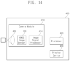
- FIG. 14 is a block diagram of an image processing device including the image sensor shown in FIG. 1 .
- an image processing device 400 includes a camera module 410 , a processor 420 , and a display device 430 .
- the image processing device 400 may be used in a mobile device, a closed circuit television (CCTV) system, a wearable computer, or an in-vehicle infotainment system, but example embodiments are not limited thereto.
- CCTV closed circuit television
- wearable computer or an in-vehicle infotainment system, but example embodiments are not limited thereto.
- the image sensor 100 of the camera module 410 captures a subject by using a lens 412 , generates an image signal corresponding to the captured subject, and transmits the image signal to an image signal processor 414 .
- a structure of the image sensor 100 may correspond to a structure of the image sensor 100 A described with reference to FIG. 12 .
- Image data processed by the image signal processor 414 may be transmitted to the processor 420 , and the processor 420 may display an image corresponding to the processed image data through the display device 430 .
- an analog-to-digital conversion circuit may convert a parallel gray code into a parallel binary code and then may directly and sequentially output, to a serial binary adder, bits of the parallel binary code from an LSB of the parallel binary code to an MSB of the parallel binary code in units of bit, while changing the arrangement of switches, thereby reducing noise while operating at high speed.
- One or more of the elements disclosed above may include or be implemented in one or more processing circuitries such as hardware including logic circuits; a hardware/software combination such as a processor executing software; or a combination thereof.
- the processing circuitries more specifically may include, but is not limited to, a central processing unit (CPU), an arithmetic logic unit (ALU), a digital signal processor, a microcomputer, a field programmable gate array (FGPA), a System-on-Chip (SoC), a programmable logic unit, a microprocessor, application-specific integrated circuit (ASIC), etc.
- CPU central processing unit
- ALU arithmetic logic unit
- FGPA field programmable gate array
- SoC System-on-Chip
- ASIC application-specific integrated circuit
Landscapes
- Engineering & Computer Science (AREA)
- Multimedia (AREA)
- Signal Processing (AREA)
- Theoretical Computer Science (AREA)
- Transforming Light Signals Into Electric Signals (AREA)
Abstract
Description
B<3>=G<3>
B<2>=G<3>⊕G<2>
B<1>=G<3>⊕G<2>⊕G<1>
B<1>=G<3>⊕G<2>⊕G<1>⊕G<0> [Equation 1]
B<1>=G<3>⊕G<2>⊕G<1>⊕0 [Equation 2]
B<2>=G<3>⊕G<2>⊕0⊕0 [Equation 3]
B<3>=G<3>⊕0⊕0⊕0 [Equation 3]
Claims (20)
Priority Applications (2)
| Application Number | Priority Date | Filing Date | Title |
|---|---|---|---|
| EP23154907.2A EP4228159A1 (en) | 2022-02-11 | 2023-02-03 | Gray code-to-binary code converter and devices including the same |
| JP2023017706A JP2023118088A (en) | 2022-02-11 | 2023-02-08 | Gray code-to-binary code converter and device containing same |
Applications Claiming Priority (4)
| Application Number | Priority Date | Filing Date | Title |
|---|---|---|---|
| KR20220018462 | 2022-02-11 | ||
| KR10-2022-0018462 | 2022-02-11 | ||
| KR1020220079026A KR20230121528A (en) | 2022-02-11 | 2022-06-28 | Gray code to binary code converter, and devices including the same |
| KR10-2022-0079026 | 2022-06-28 |
Publications (2)
| Publication Number | Publication Date |
|---|---|
| US20230262363A1 US20230262363A1 (en) | 2023-08-17 |
| US12088948B2 true US12088948B2 (en) | 2024-09-10 |
Family
ID=87558318
Family Applications (1)
| Application Number | Title | Priority Date | Filing Date |
|---|---|---|---|
| US18/064,585 Active 2043-03-08 US12088948B2 (en) | 2022-02-11 | 2022-12-12 | Gray code-to-binary code converter and devices including the same |
Country Status (1)
| Country | Link |
|---|---|
| US (1) | US12088948B2 (en) |
Cited By (1)
| Publication number | Priority date | Publication date | Assignee | Title |
|---|---|---|---|---|
| US20250142228A1 (en) * | 2023-10-26 | 2025-05-01 | Renesas Electronics Corporation | Semiconductor device, method for controlling the semiconductor device, and control program |
Families Citing this family (2)
| Publication number | Priority date | Publication date | Assignee | Title |
|---|---|---|---|---|
| KR20240131545A (en) | 2023-02-24 | 2024-09-02 | 삼성전자주식회사 | Image sensor including counter performing shifting operation and operation method thereof |
| US12526552B2 (en) * | 2023-05-23 | 2026-01-13 | Omnivision Technologies, Inc. | Sparse 4C2+ phase detection auto focus and correlated multiple sampling |
Citations (12)
| Publication number | Priority date | Publication date | Assignee | Title |
|---|---|---|---|---|
| US20130015329A1 (en) * | 2010-04-30 | 2013-01-17 | Sony Corporation | Column a/d converter, column a/d conversion method, solid-state imaging element and camera system |
| US20130068931A1 (en) * | 2010-04-30 | 2013-03-21 | Sony Corporation | A/d converter, a/d conversion method, solid-state imaging element and camera system |
| US20130335609A1 (en) * | 2011-03-30 | 2013-12-19 | Sony Corporation | A/d converter, solid-state image pickup device and driving method of the same, and electronic apparatus |
| US20150138408A1 (en) * | 2013-11-21 | 2015-05-21 | Samsung Electronics Co., Ltd. | Digital Correlated Double Sampling Circuit and Image Sensor Including the Same |
| US20150189214A1 (en) * | 2013-12-26 | 2015-07-02 | Sony Corporation | Electronic device |
| US20150326811A1 (en) * | 2012-02-29 | 2015-11-12 | Sony Corporation | Column a/d converter, column a/d conversion method, solid imaging device, and camera system |
| US20190052827A1 (en) * | 2016-04-19 | 2019-02-14 | Olympus Corporation | A/d converter, solid-state imaging device, method for driving solid-state imaging device, and electronic apparatus |
| US20190098234A1 (en) * | 2017-09-25 | 2019-03-28 | Samsung Electronics Co., Ltd. | Digital correlated double sampling circuits and image sensors including the same |
| US10841524B2 (en) | 2016-12-27 | 2020-11-17 | Sony Semiconductor Solutions Corporation | Imaging element and method for controlling imaging element, imaging apparatus, and electronic apparatus |
| US20210119639A1 (en) * | 2019-10-21 | 2021-04-22 | Samsung Electronics Co., Ltd. | Analog-to-digital converter including delay circuit and compensator, image sensor including the analog-to-digital converter, and method of operating the same |
| US20210160450A1 (en) | 2019-11-27 | 2021-05-27 | Samsung Electronics Co., Ltd. | Gray counter and image sensor including the same |
| US11133822B2 (en) | 2017-06-20 | 2021-09-28 | Sharp Kabushiki Kaisha | Analog-digital converter and solid-state imaging element |
-
2022
- 2022-12-12 US US18/064,585 patent/US12088948B2/en active Active
Patent Citations (19)
| Publication number | Priority date | Publication date | Assignee | Title |
|---|---|---|---|---|
| US20130068931A1 (en) * | 2010-04-30 | 2013-03-21 | Sony Corporation | A/d converter, a/d conversion method, solid-state imaging element and camera system |
| US20130015329A1 (en) * | 2010-04-30 | 2013-01-17 | Sony Corporation | Column a/d converter, column a/d conversion method, solid-state imaging element and camera system |
| US20130335609A1 (en) * | 2011-03-30 | 2013-12-19 | Sony Corporation | A/d converter, solid-state image pickup device and driving method of the same, and electronic apparatus |
| US9369644B2 (en) | 2011-03-30 | 2016-06-14 | Sony Corporation | A/D converter, solid-state image pickup device and driving method of the same, and electronic apparatus |
| US20150326811A1 (en) * | 2012-02-29 | 2015-11-12 | Sony Corporation | Column a/d converter, column a/d conversion method, solid imaging device, and camera system |
| US9357147B2 (en) * | 2012-02-29 | 2016-05-31 | Sony Corporation | Column A/D converter, column A/D conversion method, solid imaging device, and camera system |
| US9380246B2 (en) | 2013-11-21 | 2016-06-28 | Samsung Electronics Co., Ltd. | Digital correlated double sampling circuit and image sensor including the same |
| US20150138408A1 (en) * | 2013-11-21 | 2015-05-21 | Samsung Electronics Co., Ltd. | Digital Correlated Double Sampling Circuit and Image Sensor Including the Same |
| US20150189214A1 (en) * | 2013-12-26 | 2015-07-02 | Sony Corporation | Electronic device |
| US9762836B2 (en) * | 2013-12-26 | 2017-09-12 | Sony Corporation | Electronic device |
| US20190052827A1 (en) * | 2016-04-19 | 2019-02-14 | Olympus Corporation | A/d converter, solid-state imaging device, method for driving solid-state imaging device, and electronic apparatus |
| US10638079B2 (en) * | 2016-04-19 | 2020-04-28 | Olympus Corporation | A/D converter, solid-state imaging device, method for driving solid-state imaging device, and electronic apparatus |
| US10841524B2 (en) | 2016-12-27 | 2020-11-17 | Sony Semiconductor Solutions Corporation | Imaging element and method for controlling imaging element, imaging apparatus, and electronic apparatus |
| US11133822B2 (en) | 2017-06-20 | 2021-09-28 | Sharp Kabushiki Kaisha | Analog-digital converter and solid-state imaging element |
| US20190098234A1 (en) * | 2017-09-25 | 2019-03-28 | Samsung Electronics Co., Ltd. | Digital correlated double sampling circuits and image sensors including the same |
| US10904466B2 (en) * | 2017-09-25 | 2021-01-26 | Samsung Electronics Co., Ltd. | Digital correlated double sampling circuits and image sensors including the same |
| US20210119639A1 (en) * | 2019-10-21 | 2021-04-22 | Samsung Electronics Co., Ltd. | Analog-to-digital converter including delay circuit and compensator, image sensor including the analog-to-digital converter, and method of operating the same |
| US10992309B1 (en) | 2019-10-21 | 2021-04-27 | Samsung Electronics Co., Ltd. | Analog-to-digital converter including delay circuit and compensator, image sensor including the analog-to-digital converter, and method of operating the same |
| US20210160450A1 (en) | 2019-11-27 | 2021-05-27 | Samsung Electronics Co., Ltd. | Gray counter and image sensor including the same |
Cited By (1)
| Publication number | Priority date | Publication date | Assignee | Title |
|---|---|---|---|---|
| US20250142228A1 (en) * | 2023-10-26 | 2025-05-01 | Renesas Electronics Corporation | Semiconductor device, method for controlling the semiconductor device, and control program |
Also Published As
| Publication number | Publication date |
|---|---|
| US20230262363A1 (en) | 2023-08-17 |
Similar Documents
| Publication | Publication Date | Title |
|---|---|---|
| US12088948B2 (en) | Gray code-to-binary code converter and devices including the same | |
| CN102035539B (en) | Many haplotype datas rate counter, the data converter comprising it and imageing sensor | |
| CN102047563B (en) | Solid-state imaging device, imaging device, electronic device, AD converter, and AD conversion method | |
| JP4289206B2 (en) | Counter circuit | |
| JP4654857B2 (en) | DA converter, AD converter, semiconductor device | |
| JP5254140B2 (en) | A / D converter and solid-state imaging device including the same | |
| US9019142B2 (en) | Solid-state imaging device, imaging system, and method for driving solid-state imaging device | |
| US8711016B2 (en) | Binary-to-gray converting circuits and gray code counter including the same | |
| US9001241B2 (en) | A/D conversion circuit and image pick-up device | |
| TWI793576B (en) | Image sensor with shared gray code generator and parallel column arithmetic logic units | |
| US20110122274A1 (en) | Ddr counter circuits, analog to digital converters, image sensors and digital imaging systems including the same | |
| KR20150058792A (en) | Digital correlated double sampling circuit and image sensor including the same | |
| US8111309B2 (en) | Solid-state image pickup device and signal processing method using solid-state image pickup device | |
| JP4743227B2 (en) | AD conversion method, AD conversion apparatus, and semiconductor device and electronic apparatus for detecting physical quantity distribution | |
| WO2013175959A1 (en) | A/d converter, solid-state image pickup device and electronic device | |
| US9871986B2 (en) | Counter, counting method, ad converter, solid-state imaging device, and electronic device | |
| US8115845B2 (en) | Counter array and image sensor including the same | |
| KR20230121528A (en) | Gray code to binary code converter, and devices including the same | |
| US12244954B2 (en) | Semiconductor device | |
| EP4228159A1 (en) | Gray code-to-binary code converter and devices including the same | |
| KR102123432B1 (en) | Counter circuit and image sensor including the same | |
| CN116599536A (en) | Gray code to binary code converter and device including same | |
| US20140084140A1 (en) | Data processing circuit and solid-state imaging device | |
| US20250266843A1 (en) | Analog-to-digital converter and image sensor including the same | |
| CN210804503U (en) | Counter circuit and pixel data conversion circuit |
Legal Events
| Date | Code | Title | Description |
|---|---|---|---|
| FEPP | Fee payment procedure |
Free format text: ENTITY STATUS SET TO UNDISCOUNTED (ORIGINAL EVENT CODE: BIG.); ENTITY STATUS OF PATENT OWNER: LARGE ENTITY |
|
| AS | Assignment |
Owner name: SAMSUNG ELECTRONICS CO., LTD., KOREA, REPUBLIC OF Free format text: ASSIGNMENT OF ASSIGNORS INTEREST;ASSIGNOR:LEE, HYEOKJONG;REEL/FRAME:062173/0003 Effective date: 20221107 |
|
| STPP | Information on status: patent application and granting procedure in general |
Free format text: DOCKETED NEW CASE - READY FOR EXAMINATION |
|
| STPP | Information on status: patent application and granting procedure in general |
Free format text: NOTICE OF ALLOWANCE MAILED -- APPLICATION RECEIVED IN OFFICE OF PUBLICATIONS |
|
| STPP | Information on status: patent application and granting procedure in general |
Free format text: PUBLICATIONS -- ISSUE FEE PAYMENT VERIFIED |
|
| STCF | Information on status: patent grant |
Free format text: PATENTED CASE |