US12088188B2 - Wireless charging control method, and wireless charging transmitter and system - Google Patents
Wireless charging control method, and wireless charging transmitter and system Download PDFInfo
- Publication number
- US12088188B2 US12088188B2 US17/144,764 US202117144764A US12088188B2 US 12088188 B2 US12088188 B2 US 12088188B2 US 202117144764 A US202117144764 A US 202117144764A US 12088188 B2 US12088188 B2 US 12088188B2
- Authority
- US
- United States
- Prior art keywords
- duty cycle
- phase shift
- shift angle
- reference signal
- circuit
- Prior art date
- Legal status (The legal status is an assumption and is not a legal conclusion. Google has not performed a legal analysis and makes no representation as to the accuracy of the status listed.)
- Active, expires
Links
Images


Classifications
-
- H—ELECTRICITY
- H02—GENERATION; CONVERSION OR DISTRIBUTION OF ELECTRIC POWER
- H02M—APPARATUS FOR CONVERSION BETWEEN AC AND AC, BETWEEN AC AND DC, OR BETWEEN DC AND DC, AND FOR USE WITH MAINS OR SIMILAR POWER SUPPLY SYSTEMS; CONVERSION OF DC OR AC INPUT POWER INTO SURGE OUTPUT POWER; CONTROL OR REGULATION THEREOF
- H02M1/00—Details of apparatus for conversion
- H02M1/0067—Converter structures employing plural converter units, other than for parallel operation of the units on a single load
- H02M1/007—Plural converter units in cascade
-
- B—PERFORMING OPERATIONS; TRANSPORTING
- B60—VEHICLES IN GENERAL
- B60L—PROPULSION OF ELECTRICALLY-PROPELLED VEHICLES; SUPPLYING ELECTRIC POWER FOR AUXILIARY EQUIPMENT OF ELECTRICALLY-PROPELLED VEHICLES; ELECTRODYNAMIC BRAKE SYSTEMS FOR VEHICLES IN GENERAL; MAGNETIC SUSPENSION OR LEVITATION FOR VEHICLES; MONITORING OPERATING VARIABLES OF ELECTRICALLY-PROPELLED VEHICLES; ELECTRIC SAFETY DEVICES FOR ELECTRICALLY-PROPELLED VEHICLES
- B60L53/00—Methods of charging batteries, specially adapted for electric vehicles; Charging stations or on-board charging equipment therefor; Exchange of energy storage elements in electric vehicles
- B60L53/10—Methods of charging batteries, specially adapted for electric vehicles; Charging stations or on-board charging equipment therefor; Exchange of energy storage elements in electric vehicles characterised by the energy transfer between the charging station and the vehicle
- B60L53/12—Inductive energy transfer
- B60L53/122—Circuits or methods for driving the primary coil, e.g. supplying electric power to the coil
-
- H—ELECTRICITY
- H02—GENERATION; CONVERSION OR DISTRIBUTION OF ELECTRIC POWER
- H02J—ELECTRIC POWER NETWORKS; CIRCUIT ARRANGEMENTS OR SYSTEMS FOR SUPPLYING OR DISTRIBUTING ELECTRIC POWER; SYSTEMS FOR STORING ELECTRIC ENERGY
- H02J50/00—Circuit arrangements or systems for wireless supply or distribution of electric power
- H02J50/10—Circuit arrangements or systems for wireless supply or distribution of electric power using inductive coupling
- H02J50/12—Circuit arrangements or systems for wireless supply or distribution of electric power using inductive coupling of the resonant type
-
- H—ELECTRICITY
- H02—GENERATION; CONVERSION OR DISTRIBUTION OF ELECTRIC POWER
- H02J—ELECTRIC POWER NETWORKS; CIRCUIT ARRANGEMENTS OR SYSTEMS FOR SUPPLYING OR DISTRIBUTING ELECTRIC POWER; SYSTEMS FOR STORING ELECTRIC ENERGY
- H02J50/00—Circuit arrangements or systems for wireless supply or distribution of electric power
- H02J50/80—Circuit arrangements or systems for wireless supply or distribution of electric power involving the exchange of data, concerning supply or distribution of electric power, between transmitting devices and receiving devices
-
- H—ELECTRICITY
- H02—GENERATION; CONVERSION OR DISTRIBUTION OF ELECTRIC POWER
- H02J—ELECTRIC POWER NETWORKS; CIRCUIT ARRANGEMENTS OR SYSTEMS FOR SUPPLYING OR DISTRIBUTING ELECTRIC POWER; SYSTEMS FOR STORING ELECTRIC ENERGY
- H02J7/00—Circuit arrangements for charging or discharging batteries or for supplying loads from batteries
- H02J7/02—Circuit arrangements for charging or discharging batteries or for supplying loads from batteries for charging batteries from AC mains by converters
-
- H—ELECTRICITY
- H02—GENERATION; CONVERSION OR DISTRIBUTION OF ELECTRIC POWER
- H02M—APPARATUS FOR CONVERSION BETWEEN AC AND AC, BETWEEN AC AND DC, OR BETWEEN DC AND DC, AND FOR USE WITH MAINS OR SIMILAR POWER SUPPLY SYSTEMS; CONVERSION OF DC OR AC INPUT POWER INTO SURGE OUTPUT POWER; CONTROL OR REGULATION THEREOF
- H02M1/00—Details of apparatus for conversion
- H02M1/0048—Circuits or arrangements for reducing losses
- H02M1/0054—Transistor switching losses
- H02M1/0058—Transistor switching losses by employing soft switching techniques, i.e. commutation of transistors when applied voltage is zero or when current flow is zero
-
- H—ELECTRICITY
- H02—GENERATION; CONVERSION OR DISTRIBUTION OF ELECTRIC POWER
- H02M—APPARATUS FOR CONVERSION BETWEEN AC AND AC, BETWEEN AC AND DC, OR BETWEEN DC AND DC, AND FOR USE WITH MAINS OR SIMILAR POWER SUPPLY SYSTEMS; CONVERSION OF DC OR AC INPUT POWER INTO SURGE OUTPUT POWER; CONTROL OR REGULATION THEREOF
- H02M3/00—Conversion of DC power input into DC power output
- H02M3/01—Resonant DC/DC converters
-
- H—ELECTRICITY
- H02—GENERATION; CONVERSION OR DISTRIBUTION OF ELECTRIC POWER
- H02M—APPARATUS FOR CONVERSION BETWEEN AC AND AC, BETWEEN AC AND DC, OR BETWEEN DC AND DC, AND FOR USE WITH MAINS OR SIMILAR POWER SUPPLY SYSTEMS; CONVERSION OF DC OR AC INPUT POWER INTO SURGE OUTPUT POWER; CONTROL OR REGULATION THEREOF
- H02M3/00—Conversion of DC power input into DC power output
- H02M3/02—Conversion of DC power input into DC power output without intermediate conversion into AC
- H02M3/04—Conversion of DC power input into DC power output without intermediate conversion into AC by static converters
- H02M3/10—Conversion of DC power input into DC power output without intermediate conversion into AC by static converters using discharge tubes with control electrode or semiconductor devices with control electrode
- H02M3/145—Conversion of DC power input into DC power output without intermediate conversion into AC by static converters using discharge tubes with control electrode or semiconductor devices with control electrode using devices of a triode or transistor type requiring continuous application of a control signal
- H02M3/155—Conversion of DC power input into DC power output without intermediate conversion into AC by static converters using discharge tubes with control electrode or semiconductor devices with control electrode using devices of a triode or transistor type requiring continuous application of a control signal using semiconductor devices only
- H02M3/156—Conversion of DC power input into DC power output without intermediate conversion into AC by static converters using discharge tubes with control electrode or semiconductor devices with control electrode using devices of a triode or transistor type requiring continuous application of a control signal using semiconductor devices only with automatic control of output voltage or current, e.g. switching regulators
-
- H—ELECTRICITY
- H02—GENERATION; CONVERSION OR DISTRIBUTION OF ELECTRIC POWER
- H02M—APPARATUS FOR CONVERSION BETWEEN AC AND AC, BETWEEN AC AND DC, OR BETWEEN DC AND DC, AND FOR USE WITH MAINS OR SIMILAR POWER SUPPLY SYSTEMS; CONVERSION OF DC OR AC INPUT POWER INTO SURGE OUTPUT POWER; CONTROL OR REGULATION THEREOF
- H02M3/00—Conversion of DC power input into DC power output
- H02M3/22—Conversion of DC power input into DC power output with intermediate conversion into AC
- H02M3/24—Conversion of DC power input into DC power output with intermediate conversion into AC by static converters
- H02M3/28—Conversion of DC power input into DC power output with intermediate conversion into AC by static converters using discharge tubes with control electrode or semiconductor devices with control electrode to produce the intermediate AC
- H02M3/325—Conversion of DC power input into DC power output with intermediate conversion into AC by static converters using discharge tubes with control electrode or semiconductor devices with control electrode to produce the intermediate AC using devices of a triode or a transistor type requiring continuous application of a control signal
- H02M3/335—Conversion of DC power input into DC power output with intermediate conversion into AC by static converters using discharge tubes with control electrode or semiconductor devices with control electrode to produce the intermediate AC using devices of a triode or a transistor type requiring continuous application of a control signal using semiconductor devices only
- H02M3/33569—Conversion of DC power input into DC power output with intermediate conversion into AC by static converters using discharge tubes with control electrode or semiconductor devices with control electrode to produce the intermediate AC using devices of a triode or a transistor type requiring continuous application of a control signal using semiconductor devices only having several active switching elements
- H02M3/33573—Full-bridge at primary side of an isolation transformer
-
- H—ELECTRICITY
- H02—GENERATION; CONVERSION OR DISTRIBUTION OF ELECTRIC POWER
- H02J—ELECTRIC POWER NETWORKS; CIRCUIT ARRANGEMENTS OR SYSTEMS FOR SUPPLYING OR DISTRIBUTING ELECTRIC POWER; SYSTEMS FOR STORING ELECTRIC ENERGY
- H02J2207/00—Details of circuit arrangements for charging or discharging batteries or supplying loads from batteries
- H02J2207/20—Charging or discharging characterised by the power electronics converter
-
- Y—GENERAL TAGGING OF NEW TECHNOLOGICAL DEVELOPMENTS; GENERAL TAGGING OF CROSS-SECTIONAL TECHNOLOGIES SPANNING OVER SEVERAL SECTIONS OF THE IPC; TECHNICAL SUBJECTS COVERED BY FORMER USPC CROSS-REFERENCE ART COLLECTIONS [XRACs] AND DIGESTS
- Y02—TECHNOLOGIES OR APPLICATIONS FOR MITIGATION OR ADAPTATION AGAINST CLIMATE CHANGE
- Y02B—CLIMATE CHANGE MITIGATION TECHNOLOGIES RELATED TO BUILDINGS, e.g. HOUSING, HOUSE APPLIANCES OR RELATED END-USER APPLICATIONS
- Y02B40/00—Technologies aiming at improving the efficiency of home appliances, e.g. induction cooking or efficient technologies for refrigerators, freezers or dish washers
-
- Y—GENERAL TAGGING OF NEW TECHNOLOGICAL DEVELOPMENTS; GENERAL TAGGING OF CROSS-SECTIONAL TECHNOLOGIES SPANNING OVER SEVERAL SECTIONS OF THE IPC; TECHNICAL SUBJECTS COVERED BY FORMER USPC CROSS-REFERENCE ART COLLECTIONS [XRACs] AND DIGESTS
- Y02—TECHNOLOGIES OR APPLICATIONS FOR MITIGATION OR ADAPTATION AGAINST CLIMATE CHANGE
- Y02B—CLIMATE CHANGE MITIGATION TECHNOLOGIES RELATED TO BUILDINGS, e.g. HOUSING, HOUSE APPLIANCES OR RELATED END-USER APPLICATIONS
- Y02B70/00—Technologies for an efficient end-user side electric power management and consumption
- Y02B70/10—Technologies improving the efficiency by using switched-mode power supplies [SMPS], i.e. efficient power electronics conversion e.g. power factor correction or reduction of losses in power supplies or efficient standby modes
-
- Y—GENERAL TAGGING OF NEW TECHNOLOGICAL DEVELOPMENTS; GENERAL TAGGING OF CROSS-SECTIONAL TECHNOLOGIES SPANNING OVER SEVERAL SECTIONS OF THE IPC; TECHNICAL SUBJECTS COVERED BY FORMER USPC CROSS-REFERENCE ART COLLECTIONS [XRACs] AND DIGESTS
- Y02—TECHNOLOGIES OR APPLICATIONS FOR MITIGATION OR ADAPTATION AGAINST CLIMATE CHANGE
- Y02T—CLIMATE CHANGE MITIGATION TECHNOLOGIES RELATED TO TRANSPORTATION
- Y02T10/00—Road transport of goods or passengers
- Y02T10/60—Other road transportation technologies with climate change mitigation effect
- Y02T10/70—Energy storage systems for electromobility, e.g. batteries
-
- Y—GENERAL TAGGING OF NEW TECHNOLOGICAL DEVELOPMENTS; GENERAL TAGGING OF CROSS-SECTIONAL TECHNOLOGIES SPANNING OVER SEVERAL SECTIONS OF THE IPC; TECHNICAL SUBJECTS COVERED BY FORMER USPC CROSS-REFERENCE ART COLLECTIONS [XRACs] AND DIGESTS
- Y02—TECHNOLOGIES OR APPLICATIONS FOR MITIGATION OR ADAPTATION AGAINST CLIMATE CHANGE
- Y02T—CLIMATE CHANGE MITIGATION TECHNOLOGIES RELATED TO TRANSPORTATION
- Y02T10/00—Road transport of goods or passengers
- Y02T10/60—Other road transportation technologies with climate change mitigation effect
- Y02T10/7072—Electromobility specific charging systems or methods for batteries, ultracapacitors, supercapacitors or double-layer capacitors
-
- Y—GENERAL TAGGING OF NEW TECHNOLOGICAL DEVELOPMENTS; GENERAL TAGGING OF CROSS-SECTIONAL TECHNOLOGIES SPANNING OVER SEVERAL SECTIONS OF THE IPC; TECHNICAL SUBJECTS COVERED BY FORMER USPC CROSS-REFERENCE ART COLLECTIONS [XRACs] AND DIGESTS
- Y02—TECHNOLOGIES OR APPLICATIONS FOR MITIGATION OR ADAPTATION AGAINST CLIMATE CHANGE
- Y02T—CLIMATE CHANGE MITIGATION TECHNOLOGIES RELATED TO TRANSPORTATION
- Y02T90/00—Enabling technologies or technologies with a potential or indirect contribution to GHG emissions mitigation
- Y02T90/10—Technologies relating to charging of electric vehicles
- Y02T90/14—Plug-in electric vehicles
Definitions
- This application relates to the wireless charging field, and in particular, to a wireless charging control method, and a wireless charging transmitter and system.
- An electric vehicle charging method includes contact charging and wireless charging.
- contact charging electricity is conducted through metal contact between a plug and a socket, while during wireless charging, a coupled electromagnetic field is used as a medium to transmit electric energy.
- the wireless charging mode has the following advantages: on one hand, wireless charging is convenient and safe to use and free from issues such as sparks, risk of electric shock, dust, a contact loss, mechanical wear, and corresponding maintenance problems, and the wireless charging mode can adapt to various severe environments and weather conditions.
- wireless charging is convenient for unmanned automatic charging and mobile charging, owing to frequent charging, a capacity of a power battery installed in an electric vehicle can be greatly reduced on a premise that required endurance mileage is ensured, thereby reducing a weight of the vehicle body and improving effective utilization of energy, and wireless charging helps to reduce initial acquisition costs of electric vehicles, and resolves a high-cost problem of the electric vehicles incurred by use of large-capacity batteries, thereby promoting popularization of electric vehicles. Therefore, the application of a wireless charging technology may be one of key technologies for fueling the entire market for the electric vehicle industry.
- wireless charging systems for vehicles mostly use a magnetic resonance principle, that is, a wireless charging receiver located at the bottom of a vehicle and a wireless charging transmitter installed on the ground work together to implement non-contact charging.
- a relative position between a coil of a wireless charging transmitter (or a transmitting coil) and a coil of a wireless charging receiver (or a receiving coil) may vary, a voltage variation range of a load is relatively wide, a charging characteristic of the load changes, and the like, output impedance of an inverter circuit in the wireless charging transmitter changes. Consequently, a variation range of a current, of the transmitting coil, that needs to be adjusted in a charging process is relatively wide, resulting in a relatively large power loss of the wireless charging system.
- This application provides a wireless charging control method, and a wireless charging transmitter and system. According to technical solutions of this application, a current adjustment range of a transmitting coil can be effectively expanded to implement optimal efficiency control in a full working range, thereby reducing a power loss of a wireless charging system.
- this application provides a wireless charging transmitter, including an inner-loop control circuit, a boost circuit, an inverter circuit, and a transmitting coil, where the inner-loop control circuit is connected to both the boost circuit and the inverter circuit, and an input end and an output end of the inverter circuit are respectively connected to the boost circuit and the transmitting coil, and the inner-loop control circuit is configured to obtain a first current reference signal and a sampled current signal of the transmitting coil, compare the first current reference signal with the sampled current signal to obtain an absolute value of a difference between the first current reference signal and the sampled current signal, and adjust a phase shift angle of the inverter circuit and/or a duty cycle of the boost circuit when the absolute value is greater than a preset deviation such that after the adjustment, an absolute value of a difference between the first current reference signal and the sampled current signal of the transmitting coil is less than or equal to the preset deviation.
- phase shift angle of the inverter circuit and/or the duty cycle of the boost circuit are/is adjusted by the inner-loop control circuit such that after the adjustment, the absolute value of the difference between the first current reference signal and the first sampled current signal of the transmitting coil of the wireless charging transmitter is less than or equal to the preset deviation.
- a current adjustment range of the transmitting coil can be effectively expanded to implement optimal efficiency control in a full working range, thereby reducing a power loss of a wireless charging system.
- the inner-loop control circuit is further configured to, when the absolute value is greater than the preset deviation, and the phase shift angle of the inverter circuit is less than a maximum preset phase shift angle, increase the phase shift angle of the inverter circuit, and obtain the first current reference signal and the sampled current signal of the transmitting coil, or when the absolute value is greater than the preset deviation, the phase shift angle of the inverter circuit is greater than or equal to a maximum preset phase shift angle, and the duty cycle of the boost circuit is less than a maximum preset duty cycle, increase the duty cycle of the boost circuit, and obtain the first current reference signal and the sampled current signal of the transmitting coil.
- the inner-loop control circuit is further configured to, when the absolute value is greater than the preset deviation, and the duty cycle of the boost circuit is less than a maximum preset duty cycle, increase the duty cycle of the boost circuit, and obtain the first current reference signal and the sampled current signal of the transmitting coil, or when the absolute value is greater than the preset deviation, the duty cycle of the boost circuit is greater than or equal to a maximum preset duty cycle, and the phase shift angle of the inverter circuit is less than a maximum preset phase shift angle, increase the phase shift angle of the inverter circuit, and obtain the first current reference signal and the sampled current signal of the transmitting coil.
- the inner-loop control circuit is further configured to, when the absolute value is greater than the preset deviation, and the duty cycle of the boost circuit is greater than a minimum preset duty cycle, decrease the duty cycle of the boost circuit, and obtain the first current reference signal and the sampled current signal of the transmitting coil, or when the absolute value is greater than the preset deviation, the duty cycle of the boost circuit is less than or equal to a minimum preset duty cycle, and the phase shift angle of the inverter circuit is greater than a minimum preset phase shift angle, decrease the phase shift angle of the inverter circuit, and obtain the first current reference signal and the sampled current signal of the transmitting coil.
- the inner-loop control circuit is further configured to, when the absolute value is greater than the preset deviation, and the phase shift angle of the inverter circuit is greater than a minimum preset phase shift angle, decrease the phase shift angle of the inverter circuit, and obtain the first current reference signal and the sampled current signal of the transmitting coil, or when the absolute value is greater than the preset deviation, the phase shift angle of the inverter circuit is less than or equal to a minimum preset phase shift angle, and the duty cycle of the boost circuit is greater than a minimum preset duty cycle, decrease the duty cycle of the boost circuit.
- the inner-loop control circuit may be configured to perform adjustment in any of the foregoing four optional manners such that after the adjustment, the absolute value of the difference between the first current reference signal and the first sampled current signal of the transmitting coil of the wireless charging transmitter is less than or equal to the preset deviation. In this way, the current adjustment range of the transmitting coil can be effectively expanded to implement optimal efficiency control in the full working range, thereby reducing the power loss of the wireless charging system.
- the inner-loop control circuit includes a primary-side current compensator.
- the inner-loop control circuit is further configured to control a current of the transmitting coil using the primary-side current compensator.
- Variation ranges of the duty cycle of the boost circuit and the phase shift angle of the inverter circuit can become smaller under control using the primary-side current compensator, to implement optimal efficiency control in the full working range, thereby reducing the power loss of the wireless charging system.
- the wireless charging transmitter further includes the boost circuit configured to obtain a direct current voltage and the duty cycle of the boost circuit, and increase the direct current voltage based on the duty cycle of the boost circuit.
- Beneficial effects of the technical solution of this application include the following.
- a conduction loss of switch tubes in the inverter circuit and a voltage conversion circuit can be reduced by adding the boost circuit at an input end of the inverter circuit.
- the wireless charging transmitter further includes an outer-loop control circuit configured to obtain a second current reference signal and a second sampled current signal, or a voltage reference signal and a sampled voltage signal, and generate the first current reference signal based on the second current reference signal and the second sampled current signal or based on the voltage reference signal and the sampled voltage signal, and output the first current reference signal to the inner-loop control circuit.
- an outer-loop control circuit configured to obtain a second current reference signal and a second sampled current signal, or a voltage reference signal and a sampled voltage signal, and generate the first current reference signal based on the second current reference signal and the second sampled current signal or based on the voltage reference signal and the sampled voltage signal, and output the first current reference signal to the inner-loop control circuit.
- the following provides a wireless charging control method and a system.
- effects thereof refer to of the technical effect of the wireless charging transmitter. Details are not described again in the following.
- this application provides a wireless charging control method, including obtaining a first current reference signal and a sampled current signal of a transmitting coil, comparing the first current reference signal with the sampled current signal to obtain an absolute value of a difference between the first current reference signal and the sampled current signal, and adjusting a phase shift angle of an inverter circuit and/or a duty cycle of a boost circuit when the absolute value is greater than a preset deviation such that after the adjustment, an absolute value of a difference between the first current reference signal and the sampled current signal of the transmitting coil is less than or equal to the preset deviation.
- adjusting a phase shift angle of an inverter circuit and/or a duty cycle of a boost circuit when the absolute value is greater than a preset deviation such that after the adjustment, an absolute value of a difference between the first current reference signal and the sampled current signal of the transmitting coil is less than or equal to the preset deviation includes, when the absolute value is greater than the preset deviation, and the phase shift angle of the inverter circuit is less than a maximum preset phase shift angle, increasing the phase shift angle of the inverter circuit, and obtaining the first current reference signal and the sampled current signal of the transmitting coil, or when the absolute value is greater than the preset deviation, the phase shift angle of the inverter circuit is greater than or equal to a maximum preset phase shift angle, and the duty cycle of the boost circuit is less than a maximum preset duty cycle, increasing the duty cycle of the boost circuit, and obtaining the first current reference signal and the sampled current signal of the transmitting coil.
- adjusting a phase shift angle of an inverter circuit and/or a duty cycle of a boost circuit when the absolute value is greater than a preset deviation such that after the adjustment, an absolute value of a difference between the first current reference signal and the sampled current signal of the transmitting coil is less than or equal to the preset deviation includes, when the absolute value is greater than the preset deviation, and the duty cycle of the boost circuit is less than a maximum preset duty cycle, increasing the duty cycle of the boost circuit, and obtaining the first current reference signal and the sampled current signal of the transmitting coil, or when the absolute value is greater than the preset deviation, the duty cycle of the boost circuit is greater than or equal to a maximum preset duty cycle, and the phase shift angle of the inverter circuit is less than a maximum preset phase shift angle, increasing the phase shift angle of the inverter circuit, and obtaining the first current reference signal and the sampled current signal of the transmitting coil.
- adjusting a phase shift angle of an inverter circuit and/or a duty cycle of a boost circuit when the absolute value is greater than a preset deviation such that after the adjustment, an absolute value of a difference between the first current reference signal and the sampled current signal of the transmitting coil is less than or equal to the preset deviation includes, when the absolute value is greater than the preset deviation, and the duty cycle of the boost circuit is greater than a minimum preset duty cycle, decreasing the duty cycle of the boost circuit, and obtaining the first current reference signal and the sampled current signal of the transmitting coil, or when the absolute value is greater than the preset deviation, the duty cycle of the boost circuit is less than or equal to a minimum preset duty cycle, and the phase shift angle of the inverter circuit is greater than a minimum preset phase shift angle, decreasing the phase shift angle of the inverter circuit, and obtaining the first current reference signal and the sampled current signal of the transmitting coil.
- adjusting a phase shift angle of an inverter circuit and/or a duty cycle of a boost circuit when the absolute value is greater than a preset deviation such that after the adjustment, an absolute value of a difference between the first current reference signal and the sampled current signal of the transmitting coil is less than or equal to the preset deviation includes, when the absolute value is greater than the preset deviation, and the phase shift angle of the inverter circuit is greater than a minimum preset phase shift angle, decreasing the phase shift angle of the inverter circuit, and obtaining the first current reference signal and the sampled current signal of the transmitting coil, or when the absolute value is greater than the preset deviation, the phase shift angle of the inverter circuit is less than or equal to a minimum preset phase shift angle, and the duty cycle of the boost circuit is greater than a minimum preset duty cycle, decreasing the duty cycle of the boost circuit.
- the method further includes controlling a current of the transmitting coil using a primary-side current compensator.
- the method further includes obtaining a direct current voltage and the duty cycle of the boost circuit, and increasing the direct current voltage based on the duty cycle of the boost circuit.
- the method further includes obtaining a second current reference signal and a second sampled current signal, or a voltage reference signal and a sampled voltage signal, and generating the first current reference signal based on the second current reference signal and the second sampled current signal or based on the voltage reference signal and the sampled voltage signal, and outputting the first current reference signal to the inner-loop control circuit.
- this application provides a wireless charging system, including a wireless charging receiver and the wireless charging transmitter according to the first aspect or the optional manners of the first aspect.
- the wireless charging receiver or the wireless charging transmitter includes an outer-loop control circuit configured to obtain a second current reference signal and a second sampled current signal, or a voltage reference signal and a sampled voltage signal, and generate a first current reference signal based on the second current reference signal and the second sampled current signal or based on the voltage reference signal and the sampled voltage signal, and output the first current reference signal to an inner-loop control circuit.
- an outer-loop control circuit configured to obtain a second current reference signal and a second sampled current signal, or a voltage reference signal and a sampled voltage signal, and generate a first current reference signal based on the second current reference signal and the second sampled current signal or based on the voltage reference signal and the sampled voltage signal, and output the first current reference signal to an inner-loop control circuit.
- the wireless charging transmitter includes an inner-loop control circuit, a boost circuit, an inverter circuit, and a transmitting coil, where the inner-loop control circuit is connected to both the boost circuit and the inverter circuit, and an input end and an output end of the inverter circuit are respectively connected to the boost circuit and the transmitting coil, and the inner-loop control circuit is configured to obtain a first current reference signal and a sampled current signal of the transmitting coil, compare the first current reference signal with the sampled current signal to obtain an absolute value of a difference between the first current reference signal and the sampled current signal, and adjust a phase shift angle of the inverter circuit and/or a duty cycle of the boost circuit when the absolute value is greater than a preset deviation such that after the adjustment, an absolute value of a difference between the first current reference signal and the sampled current signal of the transmitting coil is less than or equal to the preset deviation.
- a current adjustment range of the transmitting coil can be effectively expanded to implement optimal efficiency control in a full working range, thereby reducing a power loss of a wireless charging system.
- a conduction loss of switch tubes in the inverter circuit and a voltage conversion circuit can be reduced by adding the boost circuit at an input end of the inverter circuit.
- FIG. 1 is a diagram of an application scenario of a technical solution of this application according to an embodiment of this application;
- FIG. 2 is a schematic diagram of a wireless charging system according to an embodiment of this application.
- FIG. 3 is a schematic diagram of a wireless charging system according to an embodiment of this application.
- FIG. 4 is a schematic diagram of a wireless charging system according to an embodiment of this application.
- FIG. 5 is a schematic diagram of a wireless charging system according to an embodiment of this application.
- FIG. 6 is a schematic diagram of a wireless charging system according to an embodiment of this application.
- FIG. 7 is a schematic diagram of a wireless charging system according to an embodiment of this application.
- FIG. 8 is a flowchart of a wireless charging control method according to an embodiment of this application.
- FIG. 9 A , FIG. 9 B , FIG. 9 C , and FIG. 9 D are flowcharts of four wireless charging control methods according to this application.
- Wireless charging systems for vehicles mostly use a magnetic resonance principle, that is, a wireless charging receiver located at the bottom of a vehicle and a wireless charging transmitter installed on the ground work together to implement non-contact charging.
- a magnetic resonance principle that is, a wireless charging receiver located at the bottom of a vehicle and a wireless charging transmitter installed on the ground work together to implement non-contact charging.
- a relative position between a coil of a wireless charging transmitter (or a transmitting coil) and a coil of a wireless charging receiver (or a receiving coil) may vary, a voltage variation range of a load is relatively wide, a charging characteristic of the load changes, and the like, output impedance of an inverter circuit in the wireless charging transmitter changes. Consequently, a variation range of a current, of the transmitting coil, that needs to be adjusted in a charging process is relatively wide, resulting in a relatively large power loss of the wireless charging system.
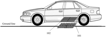
- FIG. 1 is a diagram of an application scenario of a technical solution of this application according to an embodiment of this application.
- a wireless charging transmitter 101 may be placed on the ground, or half buried or completely buried under the ground or a road, and can perform wireless charging of a vehicle (a wireless charging receiver 102 is disposed at the bottom of the vehicle) above the wireless charging transmitter 101 .
- the wireless charging transmitter 101 and the wireless charging receiver 102 perform wireless energy transmission in a manner such as electric field induction, magnetic induction, magnetic resonance, or wireless radiation, to implement wireless charging of the vehicle.
- FIG. 2 is a schematic diagram of a wireless charging system 200 according to this embodiment of this application.
- the wireless charging system 200 includes a wireless charging transmitter 201 and a wireless charging receiver 202 .
- the wireless charging transmitter 201 may include at least a boost circuit 203 , an inverter circuit 204 , a transmit-end compensation circuit 205 , a transmitting coil 206 , a transmit-end control circuit 207 , and a transmit-end wireless communications circuit 208 .
- the transmit-end control circuit 207 includes an outer-loop control circuit 209 and an inner-loop control circuit 210 .
- the wireless charging receiver 202 may include at least a receive-end control circuit 211 , a receiving coil 212 , a receive-end compensation circuit 213 , a rectifier circuit 214 , and a receive-end wireless communications circuit 215 .
- the boost circuit 203 is configured to obtain a direct current voltage and a duty cycle of the boost circuit, and increase, based on the duty cycle, the direct current voltage obtained by the boost circuit 203 .
- the direct current voltage obtained by the boost circuit 203 may be a fixed voltage or a variable voltage.
- the boost circuit 203 may be a single boost circuit, or may be a parallel circuit formed by a plurality of boost circuits.
- the inverter circuit 204 is connected to an output end of the boost circuit 203 .
- the inverter circuit 204 is configured to convert, into a high-frequency alternating current voltage, the direct current voltage output by the boost circuit 203 .
- the inverter circuit 204 may be a single-phase full-bridge structure with two bridge arms, or may be a three-phase structure with three bridge arms. That is, the inverter circuit 204 may be of a two-level structure or of a three-level structure.
- An input end of the transmit-end compensation circuit 205 is connected to an output end of the inverter circuit 204 .
- the transmit-end compensation circuit 205 is configured to compensate an equivalent impedance output by the inverter circuit 204 such that the equivalent impedance output by the inverter circuit 204 is an expected resistive impedance, inductive impedance, resistive-inductive impedance, capacitive impedance, or the like.
- the transmitting coil 206 is connected to the transmit-end compensation circuit 205 .
- the transmitting coil 206 is configured to send a high-frequency magnetic field or a high-frequency signal.
- the transmit-end control circuit 207 is connected to all of the boost circuit 203 , the inverter circuit 204 , and the transmitting coil 206 .
- the transmit-end control circuit 207 may be configured to control a first sampled current signal I pric , and implement overvoltage protection, undervoltage protection, overtemperature protection, overcurrent protection, and the like.
- the outer-loop control circuit 209 in the transmit-end control circuit 207 is configured to obtain a second current reference signal I 0_ref and a second sampled current signal I 0 , or the outer-loop control circuit 209 is configured to obtain a voltage reference signal and a sampled voltage signal.
- the following uses an example in which the outer-loop control circuit 209 obtains the second current reference signal I 0_ref and the second sampled current signal I 0 .
- the outer-loop control circuit 209 generates a first current reference signal I pric_ref based on the second current reference signal I 0_ref and the second sampled current signal I 0 under control of a controller, and outputs the first current reference signal I pric_ref to the inner-loop control circuit 210 .
- An input end of the inner-loop control circuit 210 in the transmit-end control circuit 207 is connected to an output end of the outer-loop control circuit 209 , and the inner-loop control circuit 210 is configured to obtain the first current reference signal I pric_ref and the first sampled current signal I pric of the transmitting coil of the wireless charging transmitter, compare the first current reference signal I pric_ref with the first sampled current signal I pric to obtain an absolute value of a difference between the first current reference signal I pric_ref and the first sampled current signal I pric , and if the absolute value is greater than a preset deviation ⁇ , adjust a phase shift angle ⁇ ps of the inverter circuit and/or a duty cycle D b of the boost circuit such that after the adjustment, an absolute value of a difference between the first current reference signal I pric_ref and the first sampled current signal I pric of the transmitting coil of the wireless charging transmitter is less than or equal to the preset deviation ⁇
- the transmit-end wireless communications circuit 208 exchanges information with the transmit-end control circuit 207 through a serial or parallel communications interface.
- the transmit-end wireless communications circuit 208 is configured to send and receive a control signal, a protection signal, or the like.
- the receive-end control circuit 211 is configured to control a controlled signal of the wireless charging receiver, perform analog-to-digital conversion on a sampled current signal, a sampled voltage signal, and the like, perform overvoltage protection, undervoltage protection, overtemperature protection, overcurrent protection, and the like, and send the output controlled signal to a transmit end control circuit 207 for control.
- the output signal may be a separate output current or a separate output voltage, or may be an output current and an output voltage.
- the receiving coil 212 is configured to receive the high-frequency signal or the high-frequency magnetic field transmitted by the transmitting coil 206 , and generate an induced voltage through electromagnetic induction.
- the receive-end compensation circuit 213 is configured to compensate an equivalent impedance of an input end of the rectifier circuit 214 such that the equivalent impedance of the input end of the rectifier circuit 214 is an expected resistive impedance, inductive impedance, resistive-inductive impedance, capacitive impedance, or the like.
- the receive-end compensation circuit 213 may be any combinatorial circuit including an inductor and a capacitor.
- the rectifier circuit 214 is configured to convert a signal received by the receiving coil 212 into a direct current voltage required by a load.
- the rectifier circuit 214 may be an uncontrollable circuit including a diode, a controllable circuit including a controllable switch such as a metal-oxide-semiconductor field-effect transistor (MOSFET) or an insulated-gate bipolar transistor (IGBT), a semi-controlled circuit including a thyristor, or a semi-controlled circuit including a combination of a controllable switch and an uncontrollable switch.
- MOSFET metal-oxide-semiconductor field-effect transistor
- IGBT insulated-gate bipolar transistor
- the receive-end wireless communications circuit 215 exchanges information with the receive-end control circuit 211 through a serial or parallel communications interface.
- the receive-end wireless communications circuit 215 is configured to send and receive a control signal, a protection signal, or the like.
- a control signal or a protection signal may be transmitted between the transmit-end wireless communications circuit 208 and the receive-end wireless communications circuit 215 using BLUETOOTH, WI-FI, ZIGBEE (ZIGBEE), a dedicated short-range communications technology (DSRC), or other communication modes.
- FIG. 3 is a schematic diagram of a wireless charging system 300 according to an embodiment of this application.
- the boost circuit 203 includes a power supply Vin, an inductor Lb, a diode Db, a controllable switch Qb, and a capacitor Cb.
- the inverter circuit 204 includes controllable switches S 1 , S 2 , S 3 , and S 4 .
- the transmit-end compensation circuit 205 includes an inductor L 1 , a capacitor C 1 , and a capacitor Cp.
- the outer-loop control circuit 209 includes a first comparator 301 and an output signal compensator 302 , where the first comparator 301 includes two input ends: a positive input end (represented by “+” in FIG. 3 ) and a negative input end (represented by “ ⁇ ” in FIG. 3 ), the second current reference signal I 0_ref may be input to the positive input end, and the second sampled current signal I 0 may be input to the negative input end.
- the first comparator 301 obtains a compared deviation I 0_err based on the second current reference signal I 0_ref and the second sampled current signal I 0 , and outputs the compared deviation I 0_err to the output signal compensator 302 .
- the output signal compensator 302 processes the compared deviation to obtain the first current reference signal I pric_ref .
- the inner-loop control circuit 210 includes a second comparator 303 and an inner-loop control unit 304 , where the second comparator 303 includes two input ends: a positive input end (represented by “+” in FIG. 3 ) and a negative input end (represented by “ ⁇ ” in FIG. 3 ), the first current reference signal I pric_ref may be input to the positive input end of the second comparator 303 , and the first sampled current signal I pric may be input to the negative input end of the second comparator 303 .
- the inner-loop control unit 304 calculates an absolute value of U H , and if the absolute value of U H is greater than the preset deviation ⁇ , adjusts the phase shift angle ⁇ ps of the inverter circuit and/or the duty cycle D b of the boost circuit such that after the adjustment, an absolute value of a difference between the first current reference signal I pric_ref and the first sampled current signal I pric of the transmitting coil of the wireless charging transmitter is less than or equal to the preset deviation ⁇ .
- the receive-end compensation circuit 213 includes Cs.
- the rectifier circuit 214 includes diodes D 1 , D 2 , D 3 , and D 4 .
- the wireless charging receiver 202 further includes a capacitor Co, where Co has a filtering function.
- the wireless charging receiver 202 further includes a load Vbat, where the load is usually a battery.
- the wireless charging system includes a wireless charging transmitter and a wireless charging receiver, where the wireless charging transmitter includes an inner-loop control circuit, a boost circuit, and an inverter circuit, and the inner-loop control circuit is configured to obtain a first current reference signal and a first sampled current signal of a transmitting coil of the wireless charging transmitter, compare the first current reference signal with the first sampled current signal to obtain an absolute value of a difference between the first current reference signal and the first sampled current signal, and adjust a phase shift angle of the inverter circuit and/or a duty cycle of the boost circuit when the absolute value is greater than a preset deviation such that after the adjustment, an absolute value of a difference between the first current reference signal and the first sampled current signal of the transmitting coil of the wireless charging transmitter is less than or equal to the preset deviation.
- the system can effectively expand a current adjustment range of the transmitting coil to implement optimal efficiency control in a full working range, thereby reducing a power loss of a wireless charging system. Further, in this application, a conduction loss of switch tubes in the inverter circuit and a voltage conversion circuit can be reduced by adding the boost circuit at an input end of the inverter circuit.
- FIG. 4 is a schematic diagram of a wireless charging system 400 according to this embodiment of this application.
- the inner-loop control circuit 210 further includes a primary-side current compensator 401 .
- an input end of the primary-side current compensator 401 may be connected to the second comparator 303
- an output end of the primary-side current compensator 401 may be connected to the inner-loop control unit 304 .
- the inner-loop control circuit 210 is further configured to decrease variation ranges of the duty cycle of the boost circuit 203 and the phase shift angle of the inverter circuit 204 using the primary-side current compensator 401 in order to control a current of the transmitting coil 206 .
- the primary-side current compensator may be a proportional (P) controller, a proportional-integral (PI) controller, or a proportional-integral-derivative (PID) controller in a classical control theory, or a synovial controller in a modern control theory, or the like. This is not limited herein.
- P proportional
- PI proportional-integral
- PID proportional-integral-derivative
- the inner-loop control circuit in the system further includes the primary-side current compensator. Variation ranges of a duty cycle of the boost circuit and a phase shift angle of the inverter circuit can be controlled using the primary-side current compensator, to implement optimal efficiency control in a full working range, thereby reducing a power loss of the wireless charging system.
- FIG. 5 is a schematic diagram of a wireless charging system 500 according to an embodiment of this application. As shown in FIG. 5 , the wireless charging system 500 includes a wireless charging transmitter 501 and a wireless charging receiver 502 .
- the wireless charging transmitter 501 may include at least a boost circuit 503 , an inverter circuit 504 , a transmit-end compensation circuit 505 , a transmitting coil 506 , a transmit-end control circuit 507 , and a transmit-end communications circuit 508 .
- the transmit-end control circuit 507 includes an inner-loop control circuit 509 .
- the wireless charging receiver 502 may include at least a receive-end control circuit 511 , a receiving coil 512 , a receive-end compensation circuit 513 , a rectifier circuit 514 , and a receive-end wireless communications circuit 515 .
- the receive-end control circuit 511 includes an outer-loop control circuit 510 .
- the boost circuit 503 is configured to obtain a direct current voltage and a duty cycle of the boost circuit, and increase, based on the duty cycle, the direct current voltage obtained by the boost circuit 503 .
- the direct current voltage obtained by the boost circuit 503 may be a fixed voltage or a variable voltage.
- the boost circuit 503 may be a single boost circuit, or may be a parallel circuit formed by a plurality of boost circuits.
- the inverter circuit 504 is connected to an output end of the boost circuit 503 .
- the inverter circuit 504 is configured to convert, into a high-frequency alternating current voltage, the direct current voltage output by the boost circuit 503 .
- the inverter circuit 504 may be a single-phase full-bridge structure with two bridge arms, or may be a three-phase structure with three bridge arms. That is, the inverter circuit 504 may be of a two-level structure or of a three-level structure.
- An input end of the transmit-end compensation circuit 505 is connected to an output end of the inverter circuit 504 .
- the transmit-end compensation circuit 505 is configured to compensate an equivalent impedance output by the inverter circuit 504 such that the equivalent impedance output by the inverter circuit 504 is an expected resistive impedance, inductive impedance, resistive-inductive impedance, capacitive impedance, or the like.
- the transmitting coil 506 is connected to the transmit-end compensation circuit 505 .
- the transmitting coil 506 is configured to send a high-frequency magnetic field or a high-frequency signal of the wireless charging transmitter 501 .
- the transmit-end control circuit 507 is connected to all of the boost circuit 503 , the inverter circuit 504 , and the transmitting coil 506 .
- the transmit-end control circuit 507 may be configured to perform analog-to-digital conversion, error control, and the like on a first current reference signal I pric_ref and a first sampled current signal I pric , to implement overvoltage protection, undervoltage protection, overtemperature protection, overcurrent protection, and the like.
- the outer-loop control circuit 510 in the wireless charging receiver 502 is configured to obtain a second current reference signal I 0_ref and a second sampled current signal I 0 , or the outer-loop control circuit 510 is configured to obtain a voltage reference signal and a sampled voltage signal.
- the following uses an example in which the outer-loop control circuit 510 obtains the second current reference signal I 0_ref and the second sampled current signal I 0 .
- the outer-loop control circuit 510 generates a first current reference signal I pric_ref based on the second current reference signal I 0_ref and the second sampled current signal I 0 , and outputs the first current reference signal I pric_ref to the inner-loop control circuit 509 .
- An input end of the inner-loop control circuit 509 in the transmit-end control circuit 507 is connected to an output end of the outer-loop control circuit 510 , and the inner-loop control circuit 509 is configured to obtain the first current reference signal I pric_ref and the first sampled current signal I pric of the transmitting coil of the wireless charging transmitter, compare the first current reference signal I pric_ref with the first sampled current signal I pric to obtain an absolute value of a difference between the first current reference signal I pric_ref and the first sampled current signal I pric , and if the absolute value is greater than a preset deviation ⁇ , adjust a phase shift angle ⁇ ps of the inverter circuit and/or a duty cycle D b of the boost circuit such that after the adjustment, an absolute value of a difference between the first current reference signal and the first sampled current signal of the transmitting coil of the wireless charging transmitter is less than or equal to the preset deviation.
- the transmit-end wireless communications circuit 508 exchanges information with the transmit-end control circuit 507 through a serial or parallel communications interface.
- the transmit-end wireless communications circuit 508 is configured to send and receive a control signal, a protection signal, or the like.
- the receive-end control circuit 511 is configured to control a controlled signal of the wireless charging receiver, perform analog-to-digital conversion on a sampled current signal, a sampled voltage signal, and the like, perform overvoltage protection, undervoltage protection, overtemperature protection, overcurrent protection, and the like, and send the output controlled signal to a transmit end for control.
- the output signal may be a separate output current or a separate output voltage, or may be an output current and an output voltage.
- the receiving coil 512 is configured to receive the high-frequency signal or the high-frequency magnetic field transmitted by the transmitting coil 506 , and generate an induced voltage through electromagnetic induction.
- the receive-end compensation circuit 513 is configured to compensate an equivalent impedance of an input end of the rectifier circuit 514 such that the equivalent impedance of the input end of the rectifier circuit 514 is an expected resistive impedance, inductive impedance, resistive-inductive impedance, capacitive impedance, or the like.
- the receive-end compensation circuit 513 may be any combinatorial circuit including an inductor and a capacitor.
- the rectifier circuit 514 is configured to convert a signal received by the receiving coil 512 into a direct current voltage required by a load.
- the rectifier circuit 514 may be an uncontrollable circuit including a diode, a controllable circuit including a controllable switch such as a MOSFET or an IGBT, a semi-controlled circuit including a thyristor, or a semi-controlled circuit including a combination of a controllable switch and an uncontrollable switch.
- the receive-end wireless communications circuit 515 exchanges information with the receive-end control circuit 511 through a serial or parallel communications interface.
- the receive-end wireless communications circuit 515 is configured to send and receive a control signal, a protection signal, or the like.
- a control signal or a protection signal may be transmitted between the transmit-end wireless communications circuit 508 and the receive-end wireless communications circuit 515 using BLUETOOTH, WI-FI, ZIGBEE, DSRC, or other communication modes.
- FIG. 6 is a schematic diagram of a wireless charging system 600 according to an embodiment of this application.
- the boost circuit 503 includes a power supply Vin, an inductor Lb, a diode Db, a controllable switch Qb, and a capacitor Cb.
- the inverter circuit 504 includes controllable switches S 1 , S 2 , S 3 , and S 4 .
- the transmit-end compensation circuit 505 includes an inductor L 1 , a capacitor C 1 , and a capacitor Cp.
- the outer-loop control circuit 510 includes a first comparator 601 and an output signal compensator 602 , where the first comparator 601 includes two input ends: a positive input end (represented by “+” in FIG. 6 ) and a negative input end (represented by “ ⁇ ” in FIG. 6 ), the second current reference signal I 0_ref may be input to the positive input end, and the second sampled current signal I 0 may be input to the negative input end.
- the first comparator 601 obtains a compared deviation I 0_ref based on the second current reference signal I 0_ref and the second sampled current signal I 0 , and outputs the compared deviation I 0_err to the output signal compensator 602 .
- the output signal compensator 602 processes the compared deviation I 0_err to obtain the first current reference signal I pric_ref .
- the inner-loop control circuit 509 includes a second comparator 603 and an inner-loop control unit 604 , where the second comparator 603 includes two input ends: a positive input end (represented by “+” in FIG. 6 ) and a negative input end (represented by “ ⁇ ” in FIG. 6 ), the first current reference signal I pric_ref may be input to the positive input end, and the first sampled current signal I pric may be input to the negative input end.
- the inner-loop control unit 604 calculates an absolute value of U H , and if the absolute value of U H is greater than the preset deviation ⁇ , adjusts the phase shift angle ⁇ ps of the inverter circuit and/or the duty cycle D b of the boost circuit such that after the adjustment, an absolute value of a difference between the first current reference signal I pric_ref and the first sampled current signal I pric of the transmitting coil of the wireless charging transmitter is less than or equal to the preset deviation ⁇ .
- the receive-end compensation circuit 513 includes Cs.
- the rectifier circuit 514 includes diodes D 1 , D 2 , D 3 , and D 4 .
- the wireless charging receiver 502 further includes a capacitor Co, where Co has a filtering function.
- the wireless charging receiver 502 further includes a load Vbat, where the load is usually a battery.
- Embodiment 3 a difference between Embodiment 3 and Embodiment 1 lies in that The outer-loop control circuit in Embodiment 3 is disposed in the wireless charging receiver, while the outer-loop control circuit in Embodiment 1 is disposed in the wireless charging transmitter.
- the inner-loop control circuit may be configured to adjust the phase shift angle of the inverter circuit and/or the duty cycle of the boost circuit such that after the adjustment, the absolute value of the difference between the first current reference signal and the sampled current signal of the transmitting coil of the wireless charging transmitter is less than or equal to the preset deviation.
- the system can effectively expand a current adjustment range of the transmitting coil to implement optimal efficiency control in a full working range, thereby reducing a power loss of the wireless charging system. Further, in this application, a conduction loss of switch tubes in the inverter circuit and a voltage conversion circuit can be reduced by adding the boost circuit at an input end of the inverter circuit.
- FIG. 7 is a schematic diagram of a wireless charging system 700 according to this embodiment of this application.
- the inner-loop control circuit 509 further includes a primary-side current compensator 701 .
- an input end of the primary-side current compensator 701 may be connected to the second comparator 603
- an output end of the primary-side current compensator 701 may be connected to the inner-loop control unit 604 .
- the inner-loop control circuit 509 is further configured to decrease variation ranges of the duty cycle of the boost circuit 503 and the phase shift angle of the inverter circuit 504 using the primary-side current compensator 701 in order to control a current of the transmitting coil 506 .
- the inner-loop control circuit in the system further includes the primary-side current compensator.
- the variation ranges of the duty cycle of the boost circuit and the phase shift angle of the inverter circuit can become smaller under control using the primary-side current compensator, to implement optimal efficiency control in a full working range. thereby reducing a power loss of the wireless charging system.
- the inner-loop control circuit is further configured to if the absolute value of U H is greater than the preset deviation ⁇ , determine whether the phase shift angle ⁇ ps of the inverter circuit is less than a maximum preset phase shift angle ⁇ max , or otherwise, the procedure ends, and if the phase shift angle ⁇ ps of the inverter circuit is less than the maximum preset phase shift angle ⁇ max , increase the phase shift angle ⁇ ps of the inverter circuit, and returns to the operation of obtaining the first current reference signal I pric_ref and the first sampled current signal I pric of the transmitting coil of the wireless charging transmitter, or if the phase shift angle ⁇ ps of the inverter circuit is greater than or equal to the maximum preset phase shift angle ⁇ max , determine whether the duty cycle D b of the boost circuit is less than a maximum preset duty cycle D max , and if the duty cycle D b of the boost circuit is less than the maximum preset duty cycle D max , increase
- the inner-loop control circuit is further configured to if the absolute value of U H is greater than the preset deviation ⁇ , determine whether the duty cycle D b of the boost circuit is less than a maximum preset duty cycle D max , or otherwise, the procedure ends, and if the duty cycle D b of the boost circuit is less than the maximum preset duty cycle D max , increase the duty cycle D b of the boost circuit, and obtain the first current reference signal I pric_ref and the first sampled current signal I pric of the transmitting coil of the wireless charging transmitter, or if the duty cycle D b of the boost circuit is greater than or equal to the maximum preset duty cycle D max , determine whether the phase shift angle ⁇ ps of the inverter circuit is less than a maximum preset phase shift angle ⁇ max , and if the phase shift angle ⁇ ps of the inverter circuit is less than the maximum preset phase shift angle ⁇ max , increase the phase shift angle ⁇ ps of the inverter circuit, and obtain
- the inner-loop control circuit is further configured to if the absolute value of U H is greater than the preset deviation ⁇ , determine whether the duty cycle D b of the boost circuit is greater than a minimum preset duty cycle D min, or otherwise, the procedure ends, and if the duty cycle D b of the boost circuit is greater than the minimum preset duty cycle D min , decrease the duty cycle D b of the boost circuit, and obtain the first current reference signal I pric_ref and the first sampled current signal I pric of the transmitting coil of the wireless charging transmitter, or if the duty cycle D b of the boost circuit is less than or equal to the minimum preset duty cycle D min , determine whether the phase shift angle ⁇ ps of the inverter circuit is greater than a minimum preset phase shift angle ⁇ min , and if the phase shift angle ⁇ ps of the inverter circuit is greater than the minimum preset phase shift angle ⁇ min , decrease the phase shift angle ⁇ ps of the inverter circuit, and obtain the
- the inner-loop control circuit is further configured to, if the absolute value of U H is greater than the preset deviation ⁇ , determine whether the phase shift angle ⁇ ps of the inverter circuit is greater than a minimum preset phase shift angle ⁇ min , or otherwise, the procedure ends, and if the phase shift angle ⁇ ps of the inverter circuit is greater than the minimum preset phase shift angle ⁇ min , decrease the phase shift angle ⁇ ps of the inverter circuit, and obtain the first current reference signal I pric_ref and the first sampled current signal I pric of the transmitting coil of the wireless charging transmitter, or if the phase shift angle ⁇ ps of the inverter circuit is less than or equal to the minimum preset phase shift angle ⁇ min , determine whether the duty cycle D b of the boost circuit is greater than a minimum preset duty cycle D min , and if the duty cycle D b of the boost circuit is greater than the minimum preset duty cycle D min , decrease the duty cycle D
- the outer-loop control circuit has the following functions.
- a case in which a second current reference signal I 0_ref is greater than a second sampled current signal I 0 is referred to as a power increase case, and a case in which the second current reference signal I 0_ref is less than or equal to the second sampled current signal I 0 is referred to as a power decrease case.
- a case in which a second current reference signal I 0_ref is greater than or equal to a second sampled current signal I 0 is referred to as a power increase case
- a case in which the second current reference signal I 0_ref is less than the second sampled current signal I 0 is referred to as a power decrease case.
- a power increase scenario for example, after power-on, output power needs to be gradually increased from 0 to required power.
- a power decrease scenario for example, during power-off, output power needs to be gradually decreased from a maximum value to 0.
- the outer-loop control circuit may implement any combination of the foregoing four optional manners in the power increase case and the power decrease case. For example, when the outer-loop control circuit determines that power is increased, the outer-loop control circuit sends indication information to the inner-loop control circuit such that the inner-loop control circuit uses the optional manner 1, or when the outer-loop control circuit determines that power is decreased, the outer-loop control circuit sends indication information to the inner-loop control circuit such that the inner-loop control circuit uses the optional manner 2.
- the outer-loop control circuit when the outer-loop control circuit determines that power is increased, the outer-loop control circuit sends indication information to the inner-loop control circuit such that the inner-loop control circuit uses the optional manner 1, or when the outer-loop control circuit determines that power is decreased, the outer-loop control circuit sends indication information to the inner-loop control circuit such that the inner-loop control circuit uses the optional manner 4.
- the outer-loop control circuit when the outer-loop control circuit determines that power is increased, the outer-loop control circuit sends indication information to the inner-loop control circuit such that the inner-loop control circuit uses the optional manner 3, or when the outer-loop control circuit determines that power is decreased, the outer-loop control circuit sends indication information to the inner-loop control circuit such that the inner-loop control circuit uses the optional manner 4.
- the outer-loop control circuit when the outer-loop control circuit determines that power is increased, the outer-loop control circuit sends indication information to the inner-loop control circuit such that the inner-loop control circuit uses the optional manner 3, or when the outer-loop control circuit determines that power is decreased, the outer-loop control circuit sends indication information to the inner-loop control circuit such that the inner-loop control circuit uses the optional manner 2.
- This application provides a wireless charging system, where an inner-loop control circuit may be configured to perform adjustment in any of the foregoing four optional manners such that after adjustment, an absolute value of a difference between a first current reference signal and a first sampled current signal of a transmitting coil of a wireless charging transmitter is less than or equal to a preset deviation. Therefore, the system can effectively expand a current adjustment range of the transmitting coil to implement optimal efficiency control in a full working range, thereby reducing a power loss of the wireless charging system. Further, in this application, a conduction loss of switch tubes in the inverter circuit and a voltage conversion circuit can be reduced by adding the boost circuit at an input end of the inverter circuit.
- FIG. 8 is a flowchart of a wireless charging control method according to an embodiment of this application. As shown in FIG. 8 , the method is performed by a wireless charging transmitter, an inner-loop control circuit in a wireless charging transmitter, or the like. This is not limited in this application. The method further includes the following procedure.
- Step S 801 Obtain a first current reference signal and a first sampled current signal of a transmitting coil.
- Step S 802 Compare the first current reference signal with the first sampled current signal to obtain an absolute value of a difference between the first current reference signal and the sampled current signal.
- Step S 803 Adjust a phase shift angle of an inverter circuit and/or a duty cycle of a boost circuit when the absolute value is greater than a preset deviation such that after the adjustment, an absolute value of a difference between the first current reference signal and the sampled current signal of the transmitting coil is less than or equal to the preset deviation.
- step S 803 there may be at least the following four optional manners
- FIG. 9 A to FIG. 9 D are flowcharts of four wireless charging control methods according to this application.
- a first wireless charging control method includes the following procedure.
- Step S 901 A Determine whether
- Step S 902 A Determine whether ⁇ ps ⁇ max holds true, and if ⁇ ps ⁇ max holds true, perform step S 903 A, or if ⁇ ps ⁇ max does not hold true, perform step S 904 A.
- Step S 903 A Increase the phase shift angle ⁇ px of the inverter circuit, and return to step S 801 .
- Step S 904 A Determine whether D b ⁇ D max holds true, and if D b ⁇ D max holds true, perform step S 905 A, or if D b ⁇ D max does not hold true, the procedure ends.
- Step S 905 A Increase the duty cycle D b of the boost circuit, and return to step S 801 .
- a second wireless charging control method includes the following procedure.
- Step S 901 B Determine whether
- Step S 902 B Determine whether D b ⁇ D max holds true, and if D b ⁇ D max holds true, perform step S 903 B, or if D b ⁇ D max does not hold true, perform step S 904 B.
- Step S 903 B Increase the duty cycle D b of the boost circuit, and perform step S 801 .
- Step S 904 B Determine whether ⁇ ps ⁇ max holds true, and if ⁇ ps ⁇ max holds true, perform step S 905 B, or if ⁇ ps ⁇ max does not hold true, the procedure ends.
- Step S 905 B Increase the phase shift angle ⁇ ps of the inverter circuit, and perform step S 801 .
- a third wireless charging control method includes the following procedure.
- Step S 901 C Determine whether
- Step S 902 C Determine whether D b >D min holds true, and if D b >D min holds true, perform step S 903 C, or if D b >D min does not hold true, perform step S 904 C.
- Step S 903 C Decrease the duty cycle D b of the boost circuit, and perform step S 801 .
- Step S 905 C Decrease the phase shift angle ⁇ ps of the inverter circuit, and perform step S 801 .
- a fourth wireless charging control method includes the following procedure.
- Step S 901 D Determine whether
- Step S 902 D Determine whether ⁇ ps > ⁇ min holds true, and if ⁇ ps > ⁇ min holds true, perform step S 903 D, or if ⁇ ps ⁇ min does not hold true, perform step S 904 D.
- Step S 903 D Decrease the phase shift angle ⁇ ps of the inverter circuit, and perform step S 801 .
- Step S 904 D Determine whether D b >D min holds true, and if D b >D min holds true, perform step S 905 D, or if D b >D min does not hold true, the procedure ends.
- Step S 905 D Decrease the duty cycle D b of the boost circuit, and perform step S 801 .
- the wireless charging transmitter may determine, according to the following manner, which optional manner is to be used.
- a case in which a second current reference signal I 0_ref is greater than a second sampled current signal I 0 is referred to as a power increase case, and a case in which the second current reference signal I 0_ref is less than or equal to the second sampled current signal I 0 is referred to as a power decrease case.
- a case in which a second current reference signal I 0_ref is greater than or equal to a second sampled current signal I 0 is referred to as a power increase case
- a case in which the second current reference signal I 0_ref is less than the second sampled current signal I 0 is referred to as a power decrease case.
- a power increase scenario for example, after power-on, output power needs to be gradually increased from 0 to required power.
- a power decrease scenario for example, during power-off, output power needs to be gradually decreased from a maximum value to 0.
- the outer-loop control circuit may implement any combination of the foregoing four optional manners in the power increase case and the power decrease case. For example, when the outer-loop control circuit determines that the power is increased, the outer-loop control circuit sends indication information to the inner-loop control circuit such that the inner-loop control circuit uses the optional manner 1, or when the outer-loop control circuit determines that power is decreased, the outer-loop control circuit sends indication information to the inner-loop control circuit such that the inner-loop control circuit uses the optional manner 2.
- the outer-loop control circuit when the outer-loop control circuit determines that power is increased, the outer-loop control circuit sends indication information to the inner-loop control circuit such that the inner-loop control circuit uses the optional manner 1, or when the outer-loop control circuit determines that power is decreased, the outer-loop control circuit sends indication information to the inner-loop control circuit such that the inner-loop control circuit uses the optional manner 4.
- the outer-loop control circuit when the outer-loop control circuit determines that power is increased, the outer-loop control circuit sends indication information to the inner-loop control circuit such that the inner-loop control circuit uses the optional manner 3, or when the outer-loop control circuit determines that power is decreased, the outer-loop control circuit sends indication information to the inner-loop control circuit such that the inner-loop control circuit uses the optional manner 4.
- the outer-loop control circuit when the outer-loop control circuit determines that power is increased, the outer-loop control circuit sends indication information to the inner-loop control circuit such that the inner-loop control circuit uses the optional manner 3, or when the outer-loop control circuit determines that power is decreased, the outer-loop control circuit sends indication information to the inner-loop control circuit such that the inner-loop control circuit uses the optional manner 2.
- the method further includes controlling a current of the transmitting coil using a primary-side current compensator.
- the method further includes obtaining, by the wireless charging transmitter, a direct current voltage and the duty cycle of the boost circuit, and increasing the direct current voltage based on the duty cycle of the boost circuit.
- the wireless charging method provided in this application may be performed by the wireless charging transmitter or the inner-loop control circuit in the foregoing wireless charging system. Therefore, for content and an effect of this method embodiment, refer to the content and the effect of the system embodiment. Details are not described herein again.
- This application provides a wireless charging transmitter, including an inner-loop control circuit, a boost circuit, and an inverter circuit, where the inner-loop control circuit is connected to both the boost circuit and the inverter circuit, and an output end of the boost circuit is connected to an input end of the inverter circuit, and the inner-loop control circuit is configured to obtain a first current reference signal and a second sampled current signal of a transmitting coil of the wireless charging transmitter, compare the first current reference signal with the second sampled current signal to obtain an absolute value of a difference between the first current reference signal and the second sampled current signal, and adjust a phase shift angle of the inverter circuit and/or a duty cycle of the boost circuit when the absolute value is greater than a preset deviation such that after the adjustment, an absolute value of a difference between the first current reference signal and the second sampled current signal of the transmitting coil of the wireless charging transmitter is less than or equal to the preset deviation.
- the inner-loop control circuit is further configured to, when the absolute value is greater than the preset deviation, and the phase shift angle of the inverter circuit is less than a maximum preset phase shift angle, increase the phase shift angle of the inverter circuit, and obtain the first current reference signal and the sampled current signal of the transmitting coil, or when the absolute value is greater than the preset deviation, the phase shift angle of the inverter circuit is greater than or equal to a maximum preset phase shift angle, and the duty cycle of the boost circuit is less than a maximum preset duty cycle, increase the duty cycle of the boost circuit, and obtain the first current reference signal and the sampled current signal of the transmitting coil.
- the inner-loop control circuit is further configured to, when the absolute value is greater than the preset deviation, and the duty cycle of the boost circuit is less than a maximum preset duty cycle, increase the duty cycle of the boost circuit, and obtain the first current reference signal and the sampled current signal of the transmitting coil, or when the absolute value is greater than the preset deviation, the duty cycle of the boost circuit is greater than or equal to a maximum preset duty cycle, and the phase shift angle of the inverter circuit is less than a maximum preset phase shift angle, increase the phase shift angle of the inverter circuit, and obtain the first current reference signal and the sampled current signal of the transmitting coil.
- the inner-loop control circuit is further configured to, when the absolute value is greater than the preset deviation, and the duty cycle of the boost circuit is greater than a minimum preset duty cycle, decrease the duty cycle of the boost circuit, and obtain the first current reference signal and the sampled current signal of the transmitting coil, or when the absolute value is greater than the preset deviation, the duty cycle of the boost circuit is less than or equal to a minimum preset duty cycle, and the phase shift angle of the inverter circuit is greater than a minimum preset phase shift angle, decrease the phase shift angle of the inverter circuit, and obtain the first current reference signal and the sampled current signal of the transmitting coil.
- the inner-loop control circuit is further configured to, when the absolute value is greater than the preset deviation, and the phase shift angle of the inverter circuit is greater than a minimum preset phase shift angle, decrease the phase shift angle of the inverter circuit, and obtain the first current reference signal and the sampled current signal of the transmitting coil, or when the absolute value is greater than the preset deviation, the phase shift angle of the inverter circuit is less than or equal to a minimum preset phase shift angle, and the duty cycle of the boost circuit is greater than a minimum preset duty cycle, decrease the duty cycle of the boost circuit.
- the inner-loop control circuit includes a primary-side current compensator.
- the inner-loop control circuit is further configured to control a current of the transmitting coil using the primary-side current compensator.
- the boost circuit is configured to obtain a direct current voltage and the duty cycle of the boost circuit, and increase the direct current voltage based on the duty cycle of the boost circuit.
- the wireless charging transmitter further includes an outer-loop control circuit configured to obtain a second current reference signal and a second sampled current signal, or a voltage reference signal and a sampled voltage signal, and generate the first current reference signal based on the second current reference signal and the second sampled current signal or based on the voltage reference signal and the sampled voltage signal, and output the first current reference signal to the inner-loop control circuit.
- an outer-loop control circuit configured to obtain a second current reference signal and a second sampled current signal, or a voltage reference signal and a sampled voltage signal, and generate the first current reference signal based on the second current reference signal and the second sampled current signal or based on the voltage reference signal and the sampled voltage signal, and output the first current reference signal to the inner-loop control circuit.
- the wireless charging transmitter provided in this embodiment of this application is the wireless charging transmitter in the foregoing wireless charging system. Therefore, for content and an effect of this embodiment, refer to the content and the effect of the system embodiment. Details are not described herein again.
Landscapes
- Engineering & Computer Science (AREA)
- Power Engineering (AREA)
- Computer Networks & Wireless Communication (AREA)
- Transportation (AREA)
- Mechanical Engineering (AREA)
- Charge And Discharge Circuits For Batteries Or The Like (AREA)
- Dc-Dc Converters (AREA)
Abstract
Description
Claims (20)
Applications Claiming Priority (3)
| Application Number | Priority Date | Filing Date | Title |
|---|---|---|---|
| CN201810752499.X | 2018-07-10 | ||
| CN201810752499.XA CN110707767B (en) | 2018-07-10 | 2018-07-10 | Wireless charging control method, wireless charging emitter and system |
| PCT/CN2019/077263 WO2020010861A1 (en) | 2018-07-10 | 2019-03-07 | Wireless charging control method, wireless charging transmitter and system |
Related Parent Applications (1)
| Application Number | Title | Priority Date | Filing Date |
|---|---|---|---|
| PCT/CN2019/077263 Continuation WO2020010861A1 (en) | 2018-07-10 | 2019-03-07 | Wireless charging control method, wireless charging transmitter and system |
Publications (2)
| Publication Number | Publication Date |
|---|---|
| US20210135498A1 US20210135498A1 (en) | 2021-05-06 |
| US12088188B2 true US12088188B2 (en) | 2024-09-10 |
Family
ID=69143195
Family Applications (1)
| Application Number | Title | Priority Date | Filing Date |
|---|---|---|---|
| US17/144,764 Active 2041-05-20 US12088188B2 (en) | 2018-07-10 | 2021-01-08 | Wireless charging control method, and wireless charging transmitter and system |
Country Status (5)
| Country | Link |
|---|---|
| US (1) | US12088188B2 (en) |
| EP (1) | EP3799254B1 (en) |
| CN (1) | CN110707767B (en) |
| FI (1) | FI3799254T3 (en) |
| WO (1) | WO2020010861A1 (en) |
Families Citing this family (11)
| Publication number | Priority date | Publication date | Assignee | Title |
|---|---|---|---|---|
| WO2021055473A1 (en) | 2019-09-16 | 2021-03-25 | Toyota Motor Engineering & Manufacturing North America, Inc. | Dynamic wireless power transfer base pad |
| KR102752111B1 (en) | 2019-10-30 | 2025-01-09 | 후아웨이 테크놀러지 컴퍼니 리미티드 | Wireless charging receiver, system and control method |
| CN111016694B (en) | 2019-12-17 | 2021-02-26 | 华为技术有限公司 | A wireless charging transmitter, receiver, method and system |
| CN111740504B (en) * | 2020-06-19 | 2022-05-13 | 青岛鲁渝能源科技有限公司 | Wireless charging control method and wireless charging system |
| CN112117833A (en) * | 2020-09-01 | 2020-12-22 | 珠海格力电器股份有限公司 | Thermostat charging units and thermostat devices |
| CN112615549B (en) * | 2020-12-22 | 2021-12-17 | 上海科技大学 | Novel universal four-phase shift modulation method for improving dynamic performance of double active bridges |
| CN113525149A (en) * | 2021-08-12 | 2021-10-22 | 长春捷翼汽车零部件有限公司 | Electric energy supply control method and device, electronic equipment and storage medium |
| CN115723594A (en) * | 2021-08-31 | 2023-03-03 | 华为数字能源技术有限公司 | Transmitting terminal, receiving terminal, dynamic wireless power supply system and electric automobile |
| CN115489354B (en) * | 2022-09-28 | 2025-07-01 | 中兴新能源科技有限公司 | Wireless charging startup control method, system and storage medium |
| CN118826313A (en) * | 2022-12-30 | 2024-10-22 | 荣耀终端有限公司 | A wireless charging control method and a wireless charging system |
| CN118611230B (en) * | 2024-08-06 | 2025-01-14 | 比亚迪股份有限公司 | Charging and discharging circuit, charging and discharging system and vehicle |
Citations (18)
| Publication number | Priority date | Publication date | Assignee | Title |
|---|---|---|---|---|
| CN102185533A (en) | 2011-05-23 | 2011-09-14 | 北京交通大学 | Stored energy type standard-Z source photovoltaic power generation control system and method |
| US20130033118A1 (en) * | 2011-08-04 | 2013-02-07 | Witricity Corporation | Tunable wireless power architectures |
| CN103078381A (en) | 2013-01-27 | 2013-05-01 | 中国科学院电工研究所 | Wireless charging device for electric vehicle and output control method thereof |
| CN103560599A (en) | 2013-11-18 | 2014-02-05 | 奇瑞汽车股份有限公司 | Current sampling circuit and wireless charging emitting circuit |
| CN103840528A (en) | 2014-03-19 | 2014-06-04 | 国家电网公司 | Wireless charge control method based on coordination control over voltage and frequency of power supply |
| CN104158269A (en) | 2014-08-11 | 2014-11-19 | 长城信息产业股份有限公司 | Wireless charging transmitter, receiver, charging device and wireless charging method |
| US20150061578A1 (en) * | 2013-08-30 | 2015-03-05 | Qualcomm Incorporated | System and method for alignment and compatibility detection for a wireless power transfer system |
| CN104578455A (en) | 2015-01-20 | 2015-04-29 | 中国矿业大学 | Novel high-power wireless charging system and control method thereof |
| CN104795903A (en) | 2015-04-16 | 2015-07-22 | 刘晓明 | Magnetic coupling dual-mode wireless power transmission device and control method thereof |
| CN104821667A (en) | 2015-03-16 | 2015-08-05 | 中国计量学院 | Magnetic coupling resonant wireless electric energy transmission device based on low frequency PWM rectifier |
| US20160134131A1 (en) * | 2013-07-19 | 2016-05-12 | Ihi Corporation | Power-supplying device and wireless power-supplying system |
| CN205646956U (en) | 2016-04-01 | 2016-10-12 | 杨军 | Portable three -dimensional wireless charging device of many cell -phones |
| CN106451685A (en) | 2016-12-09 | 2017-02-22 | 重庆理工大学 | Mobile phone non-contact fast charge system |
| WO2017047454A1 (en) | 2015-09-17 | 2017-03-23 | 株式会社Ihi | Power transmission device, and contactless power supply system |
| US20170222469A1 (en) * | 2016-01-28 | 2017-08-03 | Mediatek Inc. | Closed loop current control in a wireless power system |
| US20170361723A1 (en) * | 2016-06-16 | 2017-12-21 | Ford Global Technologies, Llc | Wireless charging system coil alignment |
| CN107968461A (en) | 2017-12-19 | 2018-04-27 | 北京师范大学珠海分校 | Wireless charging device and the method for automatically adjusting wireless charging device output voltage |
| US20180236879A1 (en) * | 2017-02-20 | 2018-08-23 | Ford Global Technologies, Llc | Wireless power transfer system parameter estimation |
-
2018
- 2018-07-10 CN CN201810752499.XA patent/CN110707767B/en active Active
-
2019
- 2019-03-07 WO PCT/CN2019/077263 patent/WO2020010861A1/en not_active Ceased
- 2019-03-07 FI FIEP19833239.7T patent/FI3799254T3/en active
- 2019-03-07 EP EP19833239.7A patent/EP3799254B1/en active Active
-
2021
- 2021-01-08 US US17/144,764 patent/US12088188B2/en active Active
Patent Citations (20)
| Publication number | Priority date | Publication date | Assignee | Title |
|---|---|---|---|---|
| CN102185533A (en) | 2011-05-23 | 2011-09-14 | 北京交通大学 | Stored energy type standard-Z source photovoltaic power generation control system and method |
| US20130033118A1 (en) * | 2011-08-04 | 2013-02-07 | Witricity Corporation | Tunable wireless power architectures |
| CN103843229A (en) | 2011-08-04 | 2014-06-04 | WiTricity公司 | Tunable Wireless Power Architecture |
| CN103078381A (en) | 2013-01-27 | 2013-05-01 | 中国科学院电工研究所 | Wireless charging device for electric vehicle and output control method thereof |
| US20160134131A1 (en) * | 2013-07-19 | 2016-05-12 | Ihi Corporation | Power-supplying device and wireless power-supplying system |
| US20150061578A1 (en) * | 2013-08-30 | 2015-03-05 | Qualcomm Incorporated | System and method for alignment and compatibility detection for a wireless power transfer system |
| CN103560599A (en) | 2013-11-18 | 2014-02-05 | 奇瑞汽车股份有限公司 | Current sampling circuit and wireless charging emitting circuit |
| CN103840528A (en) | 2014-03-19 | 2014-06-04 | 国家电网公司 | Wireless charge control method based on coordination control over voltage and frequency of power supply |
| CN104158269A (en) | 2014-08-11 | 2014-11-19 | 长城信息产业股份有限公司 | Wireless charging transmitter, receiver, charging device and wireless charging method |
| CN104578455A (en) | 2015-01-20 | 2015-04-29 | 中国矿业大学 | Novel high-power wireless charging system and control method thereof |
| CN104821667A (en) | 2015-03-16 | 2015-08-05 | 中国计量学院 | Magnetic coupling resonant wireless electric energy transmission device based on low frequency PWM rectifier |
| CN104795903A (en) | 2015-04-16 | 2015-07-22 | 刘晓明 | Magnetic coupling dual-mode wireless power transmission device and control method thereof |
| WO2017047454A1 (en) | 2015-09-17 | 2017-03-23 | 株式会社Ihi | Power transmission device, and contactless power supply system |
| US20170222469A1 (en) * | 2016-01-28 | 2017-08-03 | Mediatek Inc. | Closed loop current control in a wireless power system |
| CN107017706A (en) | 2016-01-28 | 2017-08-04 | 联发科技股份有限公司 | Wireless charging transmitter, system and closed-loop current control method |
| CN205646956U (en) | 2016-04-01 | 2016-10-12 | 杨军 | Portable three -dimensional wireless charging device of many cell -phones |
| US20170361723A1 (en) * | 2016-06-16 | 2017-12-21 | Ford Global Technologies, Llc | Wireless charging system coil alignment |
| CN106451685A (en) | 2016-12-09 | 2017-02-22 | 重庆理工大学 | Mobile phone non-contact fast charge system |
| US20180236879A1 (en) * | 2017-02-20 | 2018-08-23 | Ford Global Technologies, Llc | Wireless power transfer system parameter estimation |
| CN107968461A (en) | 2017-12-19 | 2018-04-27 | 北京师范大学珠海分校 | Wireless charging device and the method for automatically adjusting wireless charging device output voltage |
Also Published As
| Publication number | Publication date |
|---|---|
| CN110707767B (en) | 2021-09-21 |
| FI3799254T3 (en) | 2023-01-31 |
| WO2020010861A1 (en) | 2020-01-16 |
| EP3799254A1 (en) | 2021-03-31 |
| EP3799254B1 (en) | 2022-10-19 |
| US20210135498A1 (en) | 2021-05-06 |
| CN110707767A (en) | 2020-01-17 |
| EP3799254A4 (en) | 2021-06-09 |
Similar Documents
| Publication | Publication Date | Title |
|---|---|---|
| US12088188B2 (en) | Wireless charging control method, and wireless charging transmitter and system | |
| US11177696B2 (en) | Receive end and transmit end of wireless charging system, and wireless charging system | |
| US11901760B2 (en) | Receive end and transmit end of wireless charging system, method, electrical terminal, and system | |
| CN113765233B (en) | Electronic device and control method thereof | |
| US11190042B2 (en) | Wireless charging transmitting apparatus, transmitting method, and wireless charging system | |
| US12049144B2 (en) | Transmit end, receive end, method, and system for wireless charging | |
| CN104734315B (en) | A wireless charging control method for an electric vehicle battery | |
| WO2021082408A1 (en) | Wireless charging receiving end, system and control method | |
| CN108282035A (en) | Wireless electric energy transmission device and method suitable for anti-systematic parameter wide swings | |
| US11482941B2 (en) | Phase alignment circuit and method of receive end, and receive end | |
| WO2021083287A1 (en) | Wireless charging receiver, system and control method | |
| US20220166257A1 (en) | Wireless charging transmitting apparatus and method and wireless charging system | |
| CN109895640A (en) | A kind of electric car wireless charging two stage control system and control method | |
| WO2024140187A1 (en) | Wireless charging receiving end, wireless charging transmitting end, wireless charging system, and electric vehicle | |
| WO2023246420A1 (en) | Wireless charging system and control method therefor | |
| CN113829904B (en) | High-power wireless charging system and charging control method thereof | |
| CN210416253U (en) | Magnetic coupling resonant mode electric automobile developments wireless vehicle-mounted control device that charges | |
| CN113162165B (en) | Mutual inductance-based controllable unidirectional wireless charging control method | |
| Zheng et al. | Research on Control of Wireless Power Transfer System Based on Switched Inductor | |
| CN120150383B (en) | A wireless power transfer system suitable for industrial environments | |
| Yan et al. | A Single-Stage Constant-Power Double-Sided LCC Inductive Wireless Power Transfer Battery Charger | |
| Current | Inductively Coupled Power Transfer System |
Legal Events
| Date | Code | Title | Description |
|---|---|---|---|
| FEPP | Fee payment procedure |
Free format text: ENTITY STATUS SET TO UNDISCOUNTED (ORIGINAL EVENT CODE: BIG.); ENTITY STATUS OF PATENT OWNER: LARGE ENTITY |
|
| STPP | Information on status: patent application and granting procedure in general |
Free format text: APPLICATION DISPATCHED FROM PREEXAM, NOT YET DOCKETED |
|
| AS | Assignment |
Owner name: HUAWEI TECHNOLOGIES CO., LTD., CHINA Free format text: ASSIGNMENT OF ASSIGNORS INTEREST;ASSIGNORS:WU, ZHIXIAN;MAO, YUNHE;ZENG, XIAOSHENG;AND OTHERS;SIGNING DATES FROM 20200205 TO 20210205;REEL/FRAME:055778/0930 |
|
| STPP | Information on status: patent application and granting procedure in general |
Free format text: DOCKETED NEW CASE - READY FOR EXAMINATION |
|
| STPP | Information on status: patent application and granting procedure in general |
Free format text: NON FINAL ACTION MAILED |
|
| STPP | Information on status: patent application and granting procedure in general |
Free format text: RESPONSE TO NON-FINAL OFFICE ACTION ENTERED AND FORWARDED TO EXAMINER |
|
| STPP | Information on status: patent application and granting procedure in general |
Free format text: NON FINAL ACTION MAILED |
|
| STPP | Information on status: patent application and granting procedure in general |
Free format text: NON FINAL ACTION MAILED |
|
| STPP | Information on status: patent application and granting procedure in general |
Free format text: RESPONSE TO NON-FINAL OFFICE ACTION ENTERED AND FORWARDED TO EXAMINER |
|
| STPP | Information on status: patent application and granting procedure in general |
Free format text: NOTICE OF ALLOWANCE MAILED -- APPLICATION RECEIVED IN OFFICE OF PUBLICATIONS |
|
| STPP | Information on status: patent application and granting procedure in general |
Free format text: PUBLICATIONS -- ISSUE FEE PAYMENT VERIFIED |
|
| STCF | Information on status: patent grant |
Free format text: PATENTED CASE |