US12087770B2 - Complementary field effect transistor devices - Google Patents
Complementary field effect transistor devices Download PDFInfo
- Publication number
- US12087770B2 US12087770B2 US17/394,701 US202117394701A US12087770B2 US 12087770 B2 US12087770 B2 US 12087770B2 US 202117394701 A US202117394701 A US 202117394701A US 12087770 B2 US12087770 B2 US 12087770B2
- Authority
- US
- United States
- Prior art keywords
- fet
- cmos
- semiconductor
- stacked pair
- layers
- Prior art date
- Legal status (The legal status is an assumption and is not a legal conclusion. Google has not performed a legal analysis and makes no representation as to the accuracy of the status listed.)
- Active, expires
Links
- 230000000295 complement effect Effects 0.000 title claims abstract description 9
- 230000005669 field effect Effects 0.000 title claims description 9
- 239000004065 semiconductor Substances 0.000 claims abstract description 82
- 239000002135 nanosheet Substances 0.000 claims abstract description 39
- 229910044991 metal oxide Inorganic materials 0.000 claims abstract description 8
- 150000004706 metal oxides Chemical class 0.000 claims abstract description 8
- 125000006850 spacer group Chemical group 0.000 claims description 47
- 239000010410 layer Substances 0.000 description 94
- 239000000463 material Substances 0.000 description 86
- 238000000151 deposition Methods 0.000 description 36
- 230000008021 deposition Effects 0.000 description 28
- 238000004519 manufacturing process Methods 0.000 description 27
- 229910000577 Silicon-germanium Inorganic materials 0.000 description 26
- 229910052751 metal Inorganic materials 0.000 description 21
- 239000002184 metal Substances 0.000 description 21
- 230000015572 biosynthetic process Effects 0.000 description 20
- 239000000758 substrate Substances 0.000 description 20
- 238000000034 method Methods 0.000 description 18
- 229910052732 germanium Inorganic materials 0.000 description 14
- 229910052581 Si3N4 Inorganic materials 0.000 description 13
- GNPVGFCGXDBREM-UHFFFAOYSA-N germanium atom Chemical compound [Ge] GNPVGFCGXDBREM-UHFFFAOYSA-N 0.000 description 13
- 230000008569 process Effects 0.000 description 12
- VYPSYNLAJGMNEJ-UHFFFAOYSA-N Silicium dioxide Chemical compound O=[Si]=O VYPSYNLAJGMNEJ-UHFFFAOYSA-N 0.000 description 11
- XUIMIQQOPSSXEZ-UHFFFAOYSA-N Silicon Chemical compound [Si] XUIMIQQOPSSXEZ-UHFFFAOYSA-N 0.000 description 11
- 238000005229 chemical vapour deposition Methods 0.000 description 11
- 229910052710 silicon Inorganic materials 0.000 description 11
- 239000010703 silicon Substances 0.000 description 11
- 235000012431 wafers Nutrition 0.000 description 11
- 239000002019 doping agent Substances 0.000 description 10
- 229910045601 alloy Inorganic materials 0.000 description 9
- 239000000956 alloy Substances 0.000 description 9
- 238000005530 etching Methods 0.000 description 9
- HQVNEWCFYHHQES-UHFFFAOYSA-N silicon nitride Chemical compound N12[Si]34N5[Si]62N3[Si]51N64 HQVNEWCFYHHQES-UHFFFAOYSA-N 0.000 description 9
- 150000001875 compounds Chemical class 0.000 description 8
- 239000012535 impurity Substances 0.000 description 8
- 238000000231 atomic layer deposition Methods 0.000 description 7
- 238000001020 plasma etching Methods 0.000 description 7
- 230000001681 protective effect Effects 0.000 description 7
- 238000005137 deposition process Methods 0.000 description 6
- 239000003989 dielectric material Substances 0.000 description 6
- 238000005240 physical vapour deposition Methods 0.000 description 6
- 229910052782 aluminium Inorganic materials 0.000 description 5
- 229910052681 coesite Inorganic materials 0.000 description 5
- 229910052906 cristobalite Inorganic materials 0.000 description 5
- 238000013461 design Methods 0.000 description 5
- -1 i.e. Substances 0.000 description 5
- 239000000377 silicon dioxide Substances 0.000 description 5
- 229910052682 stishovite Inorganic materials 0.000 description 5
- 229910052905 tridymite Inorganic materials 0.000 description 5
- XAGFODPZIPBFFR-UHFFFAOYSA-N aluminium Chemical compound [Al] XAGFODPZIPBFFR-UHFFFAOYSA-N 0.000 description 4
- 239000007789 gas Substances 0.000 description 4
- 238000004518 low pressure chemical vapour deposition Methods 0.000 description 4
- 238000000623 plasma-assisted chemical vapour deposition Methods 0.000 description 4
- 239000000126 substance Substances 0.000 description 4
- ZOXJGFHDIHLPTG-UHFFFAOYSA-N Boron Chemical compound [B] ZOXJGFHDIHLPTG-UHFFFAOYSA-N 0.000 description 3
- LEVVHYCKPQWKOP-UHFFFAOYSA-N [Si].[Ge] Chemical compound [Si].[Ge] LEVVHYCKPQWKOP-UHFFFAOYSA-N 0.000 description 3
- 229910052796 boron Inorganic materials 0.000 description 3
- 238000006243 chemical reaction Methods 0.000 description 3
- 239000013078 crystal Substances 0.000 description 3
- 238000005516 engineering process Methods 0.000 description 3
- BHEPBYXIRTUNPN-UHFFFAOYSA-N hydridophosphorus(.) (triplet) Chemical compound [PH] BHEPBYXIRTUNPN-UHFFFAOYSA-N 0.000 description 3
- 239000011229 interlayer Substances 0.000 description 3
- 230000000873 masking effect Effects 0.000 description 3
- 239000000203 mixture Substances 0.000 description 3
- 150000004767 nitrides Chemical class 0.000 description 3
- 238000000059 patterning Methods 0.000 description 3
- 239000000376 reactant Substances 0.000 description 3
- 241000894007 species Species 0.000 description 3
- 238000004544 sputter deposition Methods 0.000 description 3
- 238000000992 sputter etching Methods 0.000 description 3
- 238000003860 storage Methods 0.000 description 3
- GYHNNYVSQQEPJS-UHFFFAOYSA-N Gallium Chemical compound [Ga] GYHNNYVSQQEPJS-UHFFFAOYSA-N 0.000 description 2
- UQZIWOQVLUASCR-UHFFFAOYSA-N alumane;titanium Chemical compound [AlH3].[Ti] UQZIWOQVLUASCR-UHFFFAOYSA-N 0.000 description 2
- 229910052787 antimony Inorganic materials 0.000 description 2
- WATWJIUSRGPENY-UHFFFAOYSA-N antimony atom Chemical compound [Sb] WATWJIUSRGPENY-UHFFFAOYSA-N 0.000 description 2
- 229910052785 arsenic Inorganic materials 0.000 description 2
- RQNWIZPPADIBDY-UHFFFAOYSA-N arsenic atom Chemical compound [As] RQNWIZPPADIBDY-UHFFFAOYSA-N 0.000 description 2
- 238000001505 atmospheric-pressure chemical vapour deposition Methods 0.000 description 2
- 239000007795 chemical reaction product Substances 0.000 description 2
- 230000007812 deficiency Effects 0.000 description 2
- 238000010586 diagram Methods 0.000 description 2
- 239000010408 film Substances 0.000 description 2
- 239000003574 free electron Substances 0.000 description 2
- 230000006870 function Effects 0.000 description 2
- 229910052733 gallium Inorganic materials 0.000 description 2
- 238000011065 in-situ storage Methods 0.000 description 2
- 229910052738 indium Inorganic materials 0.000 description 2
- APFVFJFRJDLVQX-UHFFFAOYSA-N indium atom Chemical compound [In] APFVFJFRJDLVQX-UHFFFAOYSA-N 0.000 description 2
- 238000002955 isolation Methods 0.000 description 2
- MRELNEQAGSRDBK-UHFFFAOYSA-N lanthanum(3+);oxygen(2-) Chemical compound [O-2].[O-2].[O-2].[La+3].[La+3] MRELNEQAGSRDBK-UHFFFAOYSA-N 0.000 description 2
- 230000000670 limiting effect Effects 0.000 description 2
- 230000003647 oxidation Effects 0.000 description 2
- 238000007254 oxidation reaction Methods 0.000 description 2
- 229910021420 polycrystalline silicon Inorganic materials 0.000 description 2
- 238000012545 processing Methods 0.000 description 2
- 239000000047 product Substances 0.000 description 2
- 238000001289 rapid thermal chemical vapour deposition Methods 0.000 description 2
- 230000002829 reductive effect Effects 0.000 description 2
- 229910052707 ruthenium Inorganic materials 0.000 description 2
- 239000012265 solid product Substances 0.000 description 2
- 229910052715 tantalum Inorganic materials 0.000 description 2
- GUVRBAGPIYLISA-UHFFFAOYSA-N tantalum atom Chemical compound [Ta] GUVRBAGPIYLISA-UHFFFAOYSA-N 0.000 description 2
- MZLGASXMSKOWSE-UHFFFAOYSA-N tantalum nitride Chemical compound [Ta]#N MZLGASXMSKOWSE-UHFFFAOYSA-N 0.000 description 2
- 239000010409 thin film Substances 0.000 description 2
- 229910052721 tungsten Inorganic materials 0.000 description 2
- 238000000038 ultrahigh vacuum chemical vapour deposition Methods 0.000 description 2
- 239000011800 void material Substances 0.000 description 2
- 229910052582 BN Inorganic materials 0.000 description 1
- PZNSFCLAULLKQX-UHFFFAOYSA-N Boron nitride Chemical compound N#B PZNSFCLAULLKQX-UHFFFAOYSA-N 0.000 description 1
- RYGMFSIKBFXOCR-UHFFFAOYSA-N Copper Chemical compound [Cu] RYGMFSIKBFXOCR-UHFFFAOYSA-N 0.000 description 1
- 241000282326 Felis catus Species 0.000 description 1
- FYYHWMGAXLPEAU-UHFFFAOYSA-N Magnesium Chemical compound [Mg] FYYHWMGAXLPEAU-UHFFFAOYSA-N 0.000 description 1
- KJTLSVCANCCWHF-UHFFFAOYSA-N Ruthenium Chemical compound [Ru] KJTLSVCANCCWHF-UHFFFAOYSA-N 0.000 description 1
- 229910020751 SixGe1-x Inorganic materials 0.000 description 1
- 229910010038 TiAl Inorganic materials 0.000 description 1
- 229910010041 TiAlC Inorganic materials 0.000 description 1
- 229910034327 TiC Inorganic materials 0.000 description 1
- ATJFFYVFTNAWJD-UHFFFAOYSA-N Tin Chemical compound [Sn] ATJFFYVFTNAWJD-UHFFFAOYSA-N 0.000 description 1
- GWEVSGVZZGPLCZ-UHFFFAOYSA-N Titan oxide Chemical compound O=[Ti]=O GWEVSGVZZGPLCZ-UHFFFAOYSA-N 0.000 description 1
- NRTOMJZYCJJWKI-UHFFFAOYSA-N Titanium nitride Chemical compound [Ti]#N NRTOMJZYCJJWKI-UHFFFAOYSA-N 0.000 description 1
- XWCMFHPRATWWFO-UHFFFAOYSA-N [O-2].[Ta+5].[Sc+3].[O-2].[O-2].[O-2] Chemical compound [O-2].[Ta+5].[Sc+3].[O-2].[O-2].[O-2] XWCMFHPRATWWFO-UHFFFAOYSA-N 0.000 description 1
- CEPICIBPGDWCRU-UHFFFAOYSA-N [Si].[Hf] Chemical compound [Si].[Hf] CEPICIBPGDWCRU-UHFFFAOYSA-N 0.000 description 1
- ILCYGSITMBHYNK-UHFFFAOYSA-N [Si]=O.[Hf] Chemical compound [Si]=O.[Hf] ILCYGSITMBHYNK-UHFFFAOYSA-N 0.000 description 1
- 239000002253 acid Substances 0.000 description 1
- 229910021417 amorphous silicon Inorganic materials 0.000 description 1
- 238000013459 approach Methods 0.000 description 1
- 238000000277 atomic layer chemical vapour deposition Methods 0.000 description 1
- VKJLWXGJGDEGSO-UHFFFAOYSA-N barium(2+);oxygen(2-);titanium(4+) Chemical compound [O-2].[O-2].[O-2].[Ti+4].[Ba+2] VKJLWXGJGDEGSO-UHFFFAOYSA-N 0.000 description 1
- 239000000919 ceramic Substances 0.000 description 1
- 239000012707 chemical precursor Substances 0.000 description 1
- 239000011248 coating agent Substances 0.000 description 1
- 238000000576 coating method Methods 0.000 description 1
- 229910017052 cobalt Inorganic materials 0.000 description 1
- 239000010941 cobalt Substances 0.000 description 1
- GUTLYIVDDKVIGB-UHFFFAOYSA-N cobalt atom Chemical compound [Co] GUTLYIVDDKVIGB-UHFFFAOYSA-N 0.000 description 1
- 238000009833 condensation Methods 0.000 description 1
- 230000005494 condensation Effects 0.000 description 1
- 239000010949 copper Substances 0.000 description 1
- 229910052802 copper Inorganic materials 0.000 description 1
- 238000000313 electron-beam-induced deposition Methods 0.000 description 1
- 238000000407 epitaxy Methods 0.000 description 1
- 238000001704 evaporation Methods 0.000 description 1
- 230000008020 evaporation Effects 0.000 description 1
- 238000011049 filling Methods 0.000 description 1
- 229910000449 hafnium oxide Inorganic materials 0.000 description 1
- WIHZLLGSGQNAGK-UHFFFAOYSA-N hafnium(4+);oxygen(2-) Chemical compound [O-2].[O-2].[Hf+4] WIHZLLGSGQNAGK-UHFFFAOYSA-N 0.000 description 1
- 230000006872 improvement Effects 0.000 description 1
- 239000013067 intermediate product Substances 0.000 description 1
- 238000007737 ion beam deposition Methods 0.000 description 1
- 238000010884 ion-beam technique Methods 0.000 description 1
- 150000002500 ions Chemical class 0.000 description 1
- 229910052746 lanthanum Inorganic materials 0.000 description 1
- FZLIPJUXYLNCLC-UHFFFAOYSA-N lanthanum atom Chemical compound [La] FZLIPJUXYLNCLC-UHFFFAOYSA-N 0.000 description 1
- JQJCSZOEVBFDKO-UHFFFAOYSA-N lead zinc Chemical compound [Zn].[Pb] JQJCSZOEVBFDKO-UHFFFAOYSA-N 0.000 description 1
- 238000001459 lithography Methods 0.000 description 1
- 229910052749 magnesium Inorganic materials 0.000 description 1
- 239000011777 magnesium Substances 0.000 description 1
- 238000001755 magnetron sputter deposition Methods 0.000 description 1
- 150000001247 metal acetylides Chemical class 0.000 description 1
- 150000002739 metals Chemical class 0.000 description 1
- 239000013081 microcrystal Substances 0.000 description 1
- 238000012986 modification Methods 0.000 description 1
- 230000004048 modification Effects 0.000 description 1
- 238000001451 molecular beam epitaxy Methods 0.000 description 1
- 239000002073 nanorod Substances 0.000 description 1
- 239000002070 nanowire Substances 0.000 description 1
- 230000007935 neutral effect Effects 0.000 description 1
- 229910052756 noble gas Inorganic materials 0.000 description 1
- 150000002835 noble gases Chemical class 0.000 description 1
- TWNQGVIAIRXVLR-UHFFFAOYSA-N oxo(oxoalumanyloxy)alumane Chemical compound O=[Al]O[Al]=O TWNQGVIAIRXVLR-UHFFFAOYSA-N 0.000 description 1
- KJXBRHIPHIVJCS-UHFFFAOYSA-N oxo(oxoalumanyloxy)lanthanum Chemical compound O=[Al]O[La]=O KJXBRHIPHIVJCS-UHFFFAOYSA-N 0.000 description 1
- SIWVEOZUMHYXCS-UHFFFAOYSA-N oxo(oxoyttriooxy)yttrium Chemical compound O=[Y]O[Y]=O SIWVEOZUMHYXCS-UHFFFAOYSA-N 0.000 description 1
- BPUBBGLMJRNUCC-UHFFFAOYSA-N oxygen(2-);tantalum(5+) Chemical compound [O-2].[O-2].[O-2].[O-2].[O-2].[Ta+5].[Ta+5] BPUBBGLMJRNUCC-UHFFFAOYSA-N 0.000 description 1
- RVTZCBVAJQQJTK-UHFFFAOYSA-N oxygen(2-);zirconium(4+) Chemical compound [O-2].[O-2].[Zr+4] RVTZCBVAJQQJTK-UHFFFAOYSA-N 0.000 description 1
- 239000002245 particle Substances 0.000 description 1
- 238000005268 plasma chemical vapour deposition Methods 0.000 description 1
- 238000002294 plasma sputter deposition Methods 0.000 description 1
- 238000007747 plating Methods 0.000 description 1
- 229920005591 polysilicon Polymers 0.000 description 1
- 230000002441 reversible effect Effects 0.000 description 1
- HBMJWWWQQXIZIP-UHFFFAOYSA-N silicon carbide Chemical compound [Si+]#[C-] HBMJWWWQQXIZIP-UHFFFAOYSA-N 0.000 description 1
- 229910010271 silicon carbide Inorganic materials 0.000 description 1
- 235000012239 silicon dioxide Nutrition 0.000 description 1
- LIVNPJMFVYWSIS-UHFFFAOYSA-N silicon monoxide Chemical compound [Si-]#[O+] LIVNPJMFVYWSIS-UHFFFAOYSA-N 0.000 description 1
- 229910052814 silicon oxide Inorganic materials 0.000 description 1
- UVGLBOPDEUYYCS-UHFFFAOYSA-N silicon zirconium Chemical compound [Si].[Zr] UVGLBOPDEUYYCS-UHFFFAOYSA-N 0.000 description 1
- 239000002904 solvent Substances 0.000 description 1
- VEALVRVVWBQVSL-UHFFFAOYSA-N strontium titanate Chemical compound [Sr+2].[O-][Ti]([O-])=O VEALVRVVWBQVSL-UHFFFAOYSA-N 0.000 description 1
- CZXRMHUWVGPWRM-UHFFFAOYSA-N strontium;barium(2+);oxygen(2-);titanium(4+) Chemical compound [O-2].[O-2].[O-2].[O-2].[Ti+4].[Sr+2].[Ba+2] CZXRMHUWVGPWRM-UHFFFAOYSA-N 0.000 description 1
- 229910001936 tantalum oxide Inorganic materials 0.000 description 1
- 229910052718 tin Inorganic materials 0.000 description 1
- OGIDPMRJRNCKJF-UHFFFAOYSA-N titanium oxide Inorganic materials [Ti]=O OGIDPMRJRNCKJF-UHFFFAOYSA-N 0.000 description 1
- WFKWXMTUELFFGS-UHFFFAOYSA-N tungsten Chemical compound [W] WFKWXMTUELFFGS-UHFFFAOYSA-N 0.000 description 1
- 239000010937 tungsten Substances 0.000 description 1
- 239000011701 zinc Substances 0.000 description 1
- 229910001928 zirconium oxide Inorganic materials 0.000 description 1
- GFQYVLUOOAAOGM-UHFFFAOYSA-N zirconium(iv) silicate Chemical compound [Zr+4].[O-][Si]([O-])([O-])[O-] GFQYVLUOOAAOGM-UHFFFAOYSA-N 0.000 description 1
Images


Classifications
-
- H01L27/092—
-
- H01L21/8221—
-
- H01L21/823871—
-
- H01L27/0688—
-
- H01L29/0673—
-
- H01L29/66439—
-
- H01L29/775—
-
- H—ELECTRICITY
- H10—SEMICONDUCTOR DEVICES; ELECTRIC SOLID-STATE DEVICES NOT OTHERWISE PROVIDED FOR
- H10D—INORGANIC ELECTRIC SEMICONDUCTOR DEVICES
- H10D30/00—Field-effect transistors [FET]
- H10D30/01—Manufacture or treatment
- H10D30/014—Manufacture or treatment of FETs having zero-dimensional [0D] or one-dimensional [1D] channels, e.g. quantum wire FETs, single-electron transistors [SET] or Coulomb blockade transistors
-
- H—ELECTRICITY
- H10—SEMICONDUCTOR DEVICES; ELECTRIC SOLID-STATE DEVICES NOT OTHERWISE PROVIDED FOR
- H10D—INORGANIC ELECTRIC SEMICONDUCTOR DEVICES
- H10D30/00—Field-effect transistors [FET]
- H10D30/01—Manufacture or treatment
- H10D30/019—Manufacture or treatment of FETs having stacked nanowire, nanosheet or nanoribbon channels
- H10D30/0198—Manufacture or treatment of FETs having stacked nanowire, nanosheet or nanoribbon channels forming source or drain electrodes wherein semiconductor bodies are replaced by dielectric layers and the source or drain electrodes extend through the dielectric layers
-
- H—ELECTRICITY
- H10—SEMICONDUCTOR DEVICES; ELECTRIC SOLID-STATE DEVICES NOT OTHERWISE PROVIDED FOR
- H10D—INORGANIC ELECTRIC SEMICONDUCTOR DEVICES
- H10D30/00—Field-effect transistors [FET]
- H10D30/40—FETs having zero-dimensional [0D], one-dimensional [1D] or two-dimensional [2D] charge carrier gas channels
- H10D30/43—FETs having zero-dimensional [0D], one-dimensional [1D] or two-dimensional [2D] charge carrier gas channels having 1D charge carrier gas channels, e.g. quantum wire FETs or transistors having 1D quantum-confined channels
-
- H—ELECTRICITY
- H10—SEMICONDUCTOR DEVICES; ELECTRIC SOLID-STATE DEVICES NOT OTHERWISE PROVIDED FOR
- H10D—INORGANIC ELECTRIC SEMICONDUCTOR DEVICES
- H10D62/00—Semiconductor bodies, or regions thereof, of devices having potential barriers
- H10D62/10—Shapes, relative sizes or dispositions of the regions of the semiconductor bodies; Shapes of the semiconductor bodies
- H10D62/117—Shapes of semiconductor bodies
- H10D62/118—Nanostructure semiconductor bodies
- H10D62/119—Nanowire, nanosheet or nanotube semiconductor bodies
- H10D62/121—Nanowire, nanosheet or nanotube semiconductor bodies oriented parallel to substrates
-
- H—ELECTRICITY
- H10—SEMICONDUCTOR DEVICES; ELECTRIC SOLID-STATE DEVICES NOT OTHERWISE PROVIDED FOR
- H10D—INORGANIC ELECTRIC SEMICONDUCTOR DEVICES
- H10D64/00—Electrodes of devices having potential barriers
- H10D64/01—Manufacture or treatment
- H10D64/017—Manufacture or treatment using dummy gates in processes wherein at least parts of the final gates are self-aligned to the dummy gates, i.e. replacement gate processes
-
- H—ELECTRICITY
- H10—SEMICONDUCTOR DEVICES; ELECTRIC SOLID-STATE DEVICES NOT OTHERWISE PROVIDED FOR
- H10D—INORGANIC ELECTRIC SEMICONDUCTOR DEVICES
- H10D84/00—Integrated devices formed in or on semiconductor substrates that comprise only semiconducting layers, e.g. on Si wafers or on GaAs-on-Si wafers
- H10D84/01—Manufacture or treatment
- H10D84/0123—Integrating together multiple components covered by H10D12/00 or H10D30/00, e.g. integrating multiple IGBTs
- H10D84/0126—Integrating together multiple components covered by H10D12/00 or H10D30/00, e.g. integrating multiple IGBTs the components including insulated gates, e.g. IGFETs
- H10D84/0165—Integrating together multiple components covered by H10D12/00 or H10D30/00, e.g. integrating multiple IGBTs the components including insulated gates, e.g. IGFETs the components including complementary IGFETs, e.g. CMOS devices
- H10D84/0186—Manufacturing their interconnections or electrodes, e.g. source or drain electrodes
-
- H—ELECTRICITY
- H10—SEMICONDUCTOR DEVICES; ELECTRIC SOLID-STATE DEVICES NOT OTHERWISE PROVIDED FOR
- H10D—INORGANIC ELECTRIC SEMICONDUCTOR DEVICES
- H10D84/00—Integrated devices formed in or on semiconductor substrates that comprise only semiconducting layers, e.g. on Si wafers or on GaAs-on-Si wafers
- H10D84/01—Manufacture or treatment
- H10D84/0123—Integrating together multiple components covered by H10D12/00 or H10D30/00, e.g. integrating multiple IGBTs
- H10D84/0126—Integrating together multiple components covered by H10D12/00 or H10D30/00, e.g. integrating multiple IGBTs the components including insulated gates, e.g. IGFETs
- H10D84/0165—Integrating together multiple components covered by H10D12/00 or H10D30/00, e.g. integrating multiple IGBTs the components including insulated gates, e.g. IGFETs the components including complementary IGFETs, e.g. CMOS devices
- H10D84/0188—Manufacturing their isolation regions
-
- H—ELECTRICITY
- H10—SEMICONDUCTOR DEVICES; ELECTRIC SOLID-STATE DEVICES NOT OTHERWISE PROVIDED FOR
- H10D—INORGANIC ELECTRIC SEMICONDUCTOR DEVICES
- H10D84/00—Integrated devices formed in or on semiconductor substrates that comprise only semiconducting layers, e.g. on Si wafers or on GaAs-on-Si wafers
- H10D84/01—Manufacture or treatment
- H10D84/02—Manufacture or treatment characterised by using material-based technologies
- H10D84/03—Manufacture or treatment characterised by using material-based technologies using Group IV technology, e.g. silicon technology or silicon-carbide [SiC] technology
- H10D84/038—Manufacture or treatment characterised by using material-based technologies using Group IV technology, e.g. silicon technology or silicon-carbide [SiC] technology using silicon technology, e.g. SiGe
-
- H—ELECTRICITY
- H10—SEMICONDUCTOR DEVICES; ELECTRIC SOLID-STATE DEVICES NOT OTHERWISE PROVIDED FOR
- H10D—INORGANIC ELECTRIC SEMICONDUCTOR DEVICES
- H10D84/00—Integrated devices formed in or on semiconductor substrates that comprise only semiconducting layers, e.g. on Si wafers or on GaAs-on-Si wafers
- H10D84/80—Integrated devices formed in or on semiconductor substrates that comprise only semiconducting layers, e.g. on Si wafers or on GaAs-on-Si wafers characterised by the integration of at least one component covered by groups H10D12/00 or H10D30/00, e.g. integration of IGFETs
- H10D84/82—Integrated devices formed in or on semiconductor substrates that comprise only semiconducting layers, e.g. on Si wafers or on GaAs-on-Si wafers characterised by the integration of at least one component covered by groups H10D12/00 or H10D30/00, e.g. integration of IGFETs of only field-effect components
- H10D84/83—Integrated devices formed in or on semiconductor substrates that comprise only semiconducting layers, e.g. on Si wafers or on GaAs-on-Si wafers characterised by the integration of at least one component covered by groups H10D12/00 or H10D30/00, e.g. integration of IGFETs of only field-effect components of only insulated-gate FETs [IGFET]
- H10D84/85—Complementary IGFETs, e.g. CMOS
-
- H—ELECTRICITY
- H10—SEMICONDUCTOR DEVICES; ELECTRIC SOLID-STATE DEVICES NOT OTHERWISE PROVIDED FOR
- H10D—INORGANIC ELECTRIC SEMICONDUCTOR DEVICES
- H10D88/00—Three-dimensional [3D] integrated devices
-
- H—ELECTRICITY
- H10—SEMICONDUCTOR DEVICES; ELECTRIC SOLID-STATE DEVICES NOT OTHERWISE PROVIDED FOR
- H10D—INORGANIC ELECTRIC SEMICONDUCTOR DEVICES
- H10D88/00—Three-dimensional [3D] integrated devices
- H10D88/01—Manufacture or treatment
-
- B—PERFORMING OPERATIONS; TRANSPORTING
- B82—NANOTECHNOLOGY
- B82Y—SPECIFIC USES OR APPLICATIONS OF NANOSTRUCTURES; MEASUREMENT OR ANALYSIS OF NANOSTRUCTURES; MANUFACTURE OR TREATMENT OF NANOSTRUCTURES
- B82Y10/00—Nanotechnology for information processing, storage or transmission, e.g. quantum computing or single electron logic
-
- H—ELECTRICITY
- H10—SEMICONDUCTOR DEVICES; ELECTRIC SOLID-STATE DEVICES NOT OTHERWISE PROVIDED FOR
- H10D—INORGANIC ELECTRIC SEMICONDUCTOR DEVICES
- H10D30/00—Field-effect transistors [FET]
- H10D30/60—Insulated-gate field-effect transistors [IGFET]
- H10D30/791—Arrangements for exerting mechanical stress on the crystal lattice of the channel regions
- H10D30/797—Arrangements for exerting mechanical stress on the crystal lattice of the channel regions being in source or drain regions, e.g. SiGe source or drain
-
- H—ELECTRICITY
- H10—SEMICONDUCTOR DEVICES; ELECTRIC SOLID-STATE DEVICES NOT OTHERWISE PROVIDED FOR
- H10D—INORGANIC ELECTRIC SEMICONDUCTOR DEVICES
- H10D62/00—Semiconductor bodies, or regions thereof, of devices having potential barriers
- H10D62/80—Semiconductor bodies, or regions thereof, of devices having potential barriers characterised by the materials
- H10D62/82—Heterojunctions
- H10D62/822—Heterojunctions comprising only Group IV materials heterojunctions, e.g. Si/Ge heterojunctions
-
- H—ELECTRICITY
- H10—SEMICONDUCTOR DEVICES; ELECTRIC SOLID-STATE DEVICES NOT OTHERWISE PROVIDED FOR
- H10D—INORGANIC ELECTRIC SEMICONDUCTOR DEVICES
- H10D64/00—Electrodes of devices having potential barriers
- H10D64/20—Electrodes characterised by their shapes, relative sizes or dispositions
- H10D64/23—Electrodes carrying the current to be rectified, amplified, oscillated or switched, e.g. sources, drains, anodes or cathodes
- H10D64/251—Source or drain electrodes for field-effect devices
-
- H—ELECTRICITY
- H10—SEMICONDUCTOR DEVICES; ELECTRIC SOLID-STATE DEVICES NOT OTHERWISE PROVIDED FOR
- H10D—INORGANIC ELECTRIC SEMICONDUCTOR DEVICES
- H10D84/00—Integrated devices formed in or on semiconductor substrates that comprise only semiconducting layers, e.g. on Si wafers or on GaAs-on-Si wafers
- H10D84/01—Manufacture or treatment
- H10D84/0123—Integrating together multiple components covered by H10D12/00 or H10D30/00, e.g. integrating multiple IGBTs
- H10D84/0126—Integrating together multiple components covered by H10D12/00 or H10D30/00, e.g. integrating multiple IGBTs the components including insulated gates, e.g. IGFETs
- H10D84/0165—Integrating together multiple components covered by H10D12/00 or H10D30/00, e.g. integrating multiple IGBTs the components including insulated gates, e.g. IGFETs the components including complementary IGFETs, e.g. CMOS devices
- H10D84/0167—Manufacturing their channels
-
- H—ELECTRICITY
- H10—SEMICONDUCTOR DEVICES; ELECTRIC SOLID-STATE DEVICES NOT OTHERWISE PROVIDED FOR
- H10D—INORGANIC ELECTRIC SEMICONDUCTOR DEVICES
- H10D84/00—Integrated devices formed in or on semiconductor substrates that comprise only semiconducting layers, e.g. on Si wafers or on GaAs-on-Si wafers
- H10D84/01—Manufacture or treatment
- H10D84/0123—Integrating together multiple components covered by H10D12/00 or H10D30/00, e.g. integrating multiple IGBTs
- H10D84/0126—Integrating together multiple components covered by H10D12/00 or H10D30/00, e.g. integrating multiple IGBTs the components including insulated gates, e.g. IGFETs
- H10D84/0165—Integrating together multiple components covered by H10D12/00 or H10D30/00, e.g. integrating multiple IGBTs the components including insulated gates, e.g. IGFETs the components including complementary IGFETs, e.g. CMOS devices
- H10D84/0172—Manufacturing their gate conductors
- H10D84/0179—Manufacturing their gate conductors the gate conductors having different shapes or dimensions
Definitions
- the disclosure relates generally to complementary field effect transistor (CFET) devices.
- the disclosure relates particularly to stacked CFET pairs having a reduced architectural footprint.
- Integrated circuit (IC) chips are formed on semiconductor wafers at increasingly smaller scale.
- transistor devices are constructed as three-dimensional (3D) field effect transistor (FET) structures.
- CMOS devices include pairs of field effect transistors (FET), an n-type FET and a p-type FET, differentiated by the nature of the elemental dopants used in their fabrication, and the resulting electrical properties.
- a complementary metal-oxide semiconductor device formed by fabricating CMOS nanosheet stacks, forming a dielectric pillar dividing the CMOS nanosheet stacks, forming CMOS FET pairs on either side of the dielectric pillar, and forming a gate contact for at least one of the FETs.
- a complementary metal-oxide semiconductor (CMOS) device includes a stacked pair of nanosheet field effect transistors (FET), the stacked pair comprising a first nanosheet device disposed above a second nanosheet device, a dielectric spacer disposed adjacent to an edge of the stacked pair, and a third FET disposed adjacent to the dielectric spacer and opposite to the stacked pair.
- FET nanosheet field effect transistors
- a complementary metal-oxide semiconductor (CMOS) device includes a stacked pair of CMOS field effect transistors (FET), the stacked pair comprising independent source/drain contacts, a dielectric spacer disposed adjacent to an edge of the stacked pair, and a third FET disposed adjacent to the dielectric spacer and opposite to the stacked pair.
- FET CMOS field effect transistors
- FIG. 1 provides a schematic plan view of a device according to an embodiment of the invention. The figure illustrates the section lines associated with the views of FIGS. 2 - 13 .
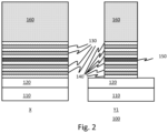
- FIG. 2 provides a cross-sectional view of a step in the fabrication of a semiconductor device, according to an embodiment of the invention.
- the figure illustrates a stack of epitaxially grown nanosheet layers and a protective hardmask layer.
- FIG. 3 provides a cross-sectional view of a step in the fabrication of a semiconductor device, according to an embodiment of the invention. The figure illustrates the device after the formation of a dielectric spacer through the stack of nanosheet layers.
- FIG. 4 provides a cross-sectional view of a step in the fabrication of a semiconductor device, according to an embodiment of the invention. The figure illustrates the device after the formation of dummy gate structures.
- FIG. 5 provides a cross-sectional view, of a step in the fabrication of a semiconductor device, according to an embodiment of the invention.
- the figure illustrates the device the epitaxial growth of CFET source/drain regions.
- FIG. 6 provides a cross-sectional view of a step in the fabrication of a semiconductor device, according to an embodiment of the invention. The figure illustrates the device after the deposition of interlayer dielectric material around the CFET devices.
- FIG. 7 provides a cross-sectional view of a step in the fabrication of a semiconductor device, according to an embodiment of the invention. The figure illustrates the device after the formation of replacement metal gate structures.
- FIG. 8 provides a cross-sectional view of a step in the fabrication of a semiconductor device, according to an embodiment of the invention. The figure illustrates the device after the formation of common gate contacts.
- FIG. 9 provides a cross-sectional view of a step in the fabrication of a semiconductor device, according to an embodiment of the invention.
- the figure illustrates the gate contacts for a CFET/unipolar device combination.
- FIG. 10 provides a cross-sectional view of a step in the fabrication of a semiconductor device, according to an embodiment of the invention. The figure illustrates the device after the formation of independent gate contacts for a CFET/CFET device combination.
- FIG. 11 provides a cross-sectional view of a step in the fabrication of a semiconductor device, according to an embodiment of the invention. The figure illustrates the device after the formation of source/drain contacts.
- FIG. 12 provides a cross-sectional view of a step in the fabrication of a semiconductor device, according to an embodiment of the invention. The figure illustrates the device after the formation of source/drain contacts.
- FIG. 13 provides a cross-sectional view of a step in the fabrication of a semiconductor device, according to an embodiment of the invention. The figure illustrates the device after the formation of source/drain contacts.
- FIG. 14 provides a flowchart depicting operational steps for forming semiconductor device, according to an embodiment of the invention.
- the present embodiments can include a design for an integrated circuit chip, which can be created in a graphical computer programming language and stored in a computer storage medium (such as a disk, tape, physical hard drive, or virtual hard drive such as in a storage access network). If the designer does not fabricate chips or the photolithographic masks used to fabricate chips, the designer can transmit the resulting design by physical means (e.g., by providing a copy of the storage medium storing the design) or electronically (e.g., through the Internet) to such entities, directly or indirectly.
- the stored design is then converted into the appropriate format (e.g., GDSII) for the fabrication of photolithographic masks, which typically include multiple copies of the chip design in question that are to be formed on a wafer.
- the photolithographic masks are utilized to define areas of the wafer (and/or the layers thereon) to be etched or otherwise processed.
- the resulting integrated circuit chips can be distributed by the fabricator in raw wafer form (that is, as a single wafer that has multiple unpackaged chips), as a bare die, or in a packaged form.
- the chip is mounted in a single chip package (such as a plastic carrier, with leads that are affixed to a motherboard or other higher-level carrier) or in a multichip package (such as a ceramic carrier that has either or both surface interconnections or buried interconnections).
- the chip is then integrated with other chips, discrete circuit elements, and/or other signal processing devices as part of either (a) an intermediate product, such as a motherboard, or (b) an end product.
- the end product can be any product that includes integrated circuit chips, ranging from toys and other low-end applications to advanced computer products having a display, a keyboard or other input device, and a central processor.
- material compounds will be described in terms of listed elements, e.g., SiGe. These compounds include different proportions of the elements within the compound, e.g., SiGe includes SixGe1-x where x is less than or equal to 1, etc.
- other elements can be included in the compound and still function in accordance with the present principles.
- the compounds with additional elements will be referred to herein as alloys.
- any of the following “/”, “and/or”, and “at least one of”, for example, in the cases of “A/B”, “A and/or B” and “at least one of A and B”, is intended to encompass the selection of the first listed option (A) only, or the selection of the second listed option (B) only, or the selection of both options (A and B).
- such phrasing is intended to encompass the selection of the first listed option (A) only, or the selection of the second listed option (B) only, or the selection of the third listed option (C) only, or the selection of the first and the second listed options (A and B) only, or the selection of the first and third listed options (A and C) only, or the selection of the second and third listed options (B and C) only, or the selection of all three options (A and B and C).
- This can be extended, as readily apparent by one of ordinary skill in this and related arts, for as many items listed.
- spatially relative terms such as “beneath,” “below,” “lower,” “above,” “upper,” and the like, can be used herein for ease of description to describe one element's or feature's relationship to another element(s) or feature(s) as illustrated in the FIGS. It will be understood that the spatially relative terms are intended to encompass different orientations of the device in use or operation in addition to the orientation depicted in the FIGS. For example, if the device in the FIGS. is turned over, elements described as “below” or “beneath” other elements or features would then be oriented “above” the other elements or features. Thus, the term “below” can encompass both an orientation of above and below.
- the device can be otherwise oriented (rotated 90 degrees or at other orientations and the spatially relative descriptors used herein can be interpreted accordingly.
- a layer when referred to as being “between” two layers, it can be the only layer between the two layers, or one or more intervening layers cat also be present.
- Deposition processes for the metal liner and sacrificial material include, e.g., chemical vapor deposition (CVD), physical vapor deposition (PVD), atomic layer deposition (ALD), or gas cluster ion beam (GCIB) deposition.
- CVD is a deposition process in which a deposited species is formed as a result of chemical reaction between gaseous reactants at greater than room temperature (e.g., from about 25° C. about 900° C.). The solid product of the reaction is deposited on the surface on which a film, coating, or layer of the solid product is to be formed.
- CVD processes include, but are not limited to, Atmospheric Pressure CVD (APCVD), Low Pressure CVD (LPCVD), Plasma Enhanced CVD (PECVD), and Metal-Organic CVD (MOCVD) and combinations thereof may also be employed.
- APCVD Atmospheric Pressure CVD
- LPCVD Low Pressure CVD
- PECVD Plasma Enhanced CVD
- MOCVD Metal-Organic CVD
- a sputtering apparatus may include direct-current diode systems, radio frequency sputtering, magnetron sputtering, or ionized metal plasma sputtering.
- chemical precursors react with the surface of a material one at a time to deposit a thin film on the surface.
- a high-pressure gas is allowed to expand in a vacuum, subsequently condensing into clusters.
- the clusters can be ionized and directed onto a surface, providing a highly anisotropic deposition.
- Integrated circuit (IC) chips are formed on semiconductor wafers at increasingly smaller scale.
- transistor devices are constructed as three-dimensional (3D) field effect transistor (FET) structures.
- FET field effect transistor
- chipmakers face a myriad of challenges at 5 nm, 3 nm and beyond.
- chip scaling continues to slow as process complexities and costs escalate at each node.
- Disclosed embodiments enable reduced footprints for CMOS device architectures through the formation of pairs CMOS devices from a single stack of nanosheet layers grown upon an underlying substrate.
- the figures provide schematic cross-sectional illustration of semiconductor devices at intermediate stages of fabrication, according to one or more embodiments of the invention.
- the figures provide a front cross-section taken along section line X of FIG. 1 , and a side cross-section taken along section line Y 1 of the plan view of FIG. 1 .
- the device provide schematic representations of the devices of the invention and are not to be considered accurate or limiting with regards to device element scale.
- FIG. 1 provides a plan view of two CFET device pairs after fabrication steps disclosed herein.
- gate structures 12 are disposed perpendicular to nanosheet stack 14 .
- Section lines X, Y 1 , and Y 2 indicate the viewpoints of the respective views of FIGS. 2 - 13 .
- FIG. 2 provides a schematic view of a device 100 according to an embodiment of the invention following the deposition, patterning, and selective removal of a stack of layers for the formation of CFET device nanosheets.
- the stack includes alternating layers of epitaxially grown silicon germanium 140 , 150 , and silicon 130 . Other materials having similar properties may be used in place of the SiGe and Si.
- epitaxially growing and/or depositing and “epitaxially grown and/or deposited” mean the growth of a semiconductor material on a deposition surface of a semiconductor material, in which the semiconductor material being grown has the same crystalline characteristics as the semiconductor material of the deposition surface.
- the chemical reactants provided by the source gases are controlled and the system parameters are set so that the depositing atoms arrive at the deposition surface of the semiconductor substrate with sufficient energy to move around on the surface and orient themselves to the crystal arrangement of the atoms of the deposition surface. Therefore, an epitaxial semiconductor material has the same crystalline characteristics as the deposition surface on which it is formed.
- the nanosheet stack includes a bottom-most layer 140 and a top-most layer 140 of a first semiconductor material, such as SiGe and an intervening layers 130 of a second semiconductor material, such as Si.
- the nanosheet stack is depicted with eleven layers (three SiGe layers and two Si layers forming a lower device, three SiGe layers and two Si layers forming an upper device, and a high Ge concertation, e.g., 50%-70% Ge, SiGe layer 150 , separating the upper and lower device layer sets), however any number and combination of layers can be used so long as the layers alternate between SiGe and Si to form lower and upper devices and include a high Ge concentration SiGe layer separating the lower and upper devices.
- SiGe layers 140 , 150 can be composed of, for instance, SiGe 20-60 , examples thereof including, but not limited to SiGe 20 , SiGe 25 , SiGe 30 . . . SiGe 65 .
- An insulating layer 120 may be present on substrate 110 and, if present, is located between substrate 110 and the nanosheet stack. Insulating layer 120 can be, for example, a buried oxide layer (typically SiO 2 ) or a bottom dielectric isolation layer formed early in the process (typically SiN, SiBCN, SiOCN, SiOC, or any combination of low-k materials).
- each sacrificial semiconductor material layer 140 and 150 is composed of a first semiconductor material which differs in composition from at least an upper portion of the semiconductor substrate 110 .
- the upper portion of the semiconductor substrate 110 is composed of silicon
- each sacrificial semiconductor material layers 140 and 150 is composed of a silicon germanium alloy.
- the SiGe alloy that provides each sacrificial semiconductor material layer 150 has a germanium content that is greater than 50 atomic percent germanium.
- the SiGe alloy that provides each sacrificial semiconductor material layer 150 has a germanium content from 50 atomic percent germanium to 70 atomic percent germanium.
- the SiGe alloy that provides each sacrificial semiconductor material layer 140 has a germanium content that is less than 50 atomic percent germanium. In one example, the SiGe alloy that provides each sacrificial semiconductor material layer 140 has a germanium content from 20 atomic percent germanium to 40 atomic percent germanium.
- the first semiconductor material that provides each sacrificial semiconductor material layers 140 and 150 can be formed utilizing an epitaxial growth (or deposition process).
- Each semiconductor channel material layer 130 is composed of a second semiconductor material that has a different etch rate than the first semiconductor material of the sacrificial semiconductor material layers 140 and 150 and is also resistant to Ge condensation.
- the second semiconductor material of each semiconductor channel material layer 130 may be the same as, or different from, the semiconductor material of at least the upper portion of the semiconductor substrate 110 .
- the second semiconductor material can be a SiGe alloy provided that the SiGe alloy has a germanium content that is less than 50 atomic percent germanium, and that the first semiconductor material is different from the second semiconductor material.
- each semiconductor channel material layer 130 is composed of Si or a III-V compound semiconductor, while each sacrificial semiconductor material layer 140 , 150 is composed of a silicon germanium alloy.
- the second semiconductor material of each semiconductor channel material layer 130 can be formed utilizing an epitaxial growth (or deposition process).
- hardmask 160 is deposited above the stack of nanosheet layers 130 - 150 .
- hardmask 160 includes a nitride, oxide, an oxide-nitride bilayer, or another suitable material.
- the hardmask 160 may include an oxide such as silicon oxide (SiO), a nitride such as silicon nitride (SiN), an oxynitride such as silicon oxynitride (SiON), combinations thereof, etc.
- the hardmask 160 is a silicon nitride such as Si 3 N 4 .
- the layers are patterned using a process such as lithographic masking, and selectively etched yielding a pattern of device fins including stacks of upper and lower device nanosheets separated by sacrificial layers of semiconductor materials, which defines the active region of the devices, and protected above by hardmask layer 160 .
- FIG. 3 illustrates device 100 following the formation of dielectric spacer 220 .
- a protective mask 210 such as an organic planarization layer (OPL)
- OPL organic planarization layer
- a trench is then etched through the hardmask 160 and nanosheet stacks using Reactive ion etching (RIE) or similar methods, to the upper surface of insulating layer 120 .
- spacer material 220 may be comprised of any one or more of a variety of different insulative materials, such as Si 3 N 4 , SiBCN, SiNC, SiN, SiCO, SiO 2 , SiNOC, etc.
- FIG. 4 illustrates device 100 following removal of the OPL and hard mask 160 from the device.
- the Figure further shows the device following fabrication of dummy gate structures including dummy gates 320 , and sacrificial caps 310 .
- Formation of dummy gate structures includes the deposition and subsequent patterning the sacrificial cap and dummy gate layers. Three dummy gates are shown however any number of gates can be formed.
- Dummy gate structures can be formed by depositing a dummy gate material 320 over the nanosheet stack.
- “Depositing” may include any now known or later developed techniques appropriate for the material to be deposited including but not limited to, for example: chemical vapor deposition (CVD), low-pressure CVD (LPCVD), plasma-enhanced CVD (PECVD), semi-atmosphere CVD (SACVD) and high density plasma CVD (HDPCVD), rapid thermal CVD (RTCVD), ultra-high vacuum CVD (UHVCVD), limited reaction processing CVD (LRPCVD), metalorganic CVD (MOCVD), sputtering deposition, ion beam deposition, electron beam deposition, laser assisted deposition, thermal oxidation, thermal nitridation, spin-on methods, physical vapor deposition (PVD), atomic layer deposition (ALD), chemical oxidation, molecular beam epitaxy (MBE), plating, evaporation.
- CVD chemical vapor deposition
- LPCVD low-pressure CVD
- PECVD plasma-enhanced CVD
- SACVD
- FIG. 5 illustrates device 100 following formation of CFET device stacks and growth of device source/drain regions 430 , 440 , separated by a dielectric material 450 .
- the Figure further illustrates the formation of gate sidewall spacer 420 , adjacent to the dummy gates, as well as inner spacers 410 , between channel nanosheets of the upper and lower FET devices of the CMOS stacks.
- FIG. 5 illustrates device 100 following selective removal of sacrificial layer 150 separating the upper and lower FET devices of the CFET.
- the high Ge concentration SiGe of layer 150 may be selectively etched away without removal of sacrificial layers 140 , or channel layers 130 , due to the higher concentration of Ge of sacrificial layer 150 compared to sacrificial layers 140 , or channel layers 130 .
- FIG. 5 illustrates device 100 following conformal deposition and selective etching of spacer materials to fill the void left by removal of layer 150 .
- Spacer material 420 further forms sidewall spacers along the sidewalls of dummy gate structure 320 and hardmask 310 .
- spacer material 420 may be the same material as hardmask 160 , or may be different materials and may be comprised of any one or more of a variety of different insulative materials, such as Si 3 N 4 , SiBCN, SiNC, SiN, SiCO, SiO 2 , SiNOC, etc.
- selective etching such as anisotropic reactive ion etching, removes spacer material 420 from horizontal surfaces of the intermediate stage of the device 100 .
- FIG. 5 further illustrates device 100 following recessing the nanosheet stack layers 130 , 140 , and spacer layer 420 , to form the S/D cavities for CFET devices.
- FIG. 5 illustrates device 100 following formation of inner spacers 410 between nanosheets of the respective FET devices. Portions of nanosheet stack layers 130 , 140 , and spacers 420 , which are not underneath gate spacers 420 and not underneath dummy gate 320 are removed.
- Etching generally refers to the removal of material from a substrate (or structures formed on the substrate) and is often performed with a mask in place so that material may selectively be removed from certain areas of the substrate, while leaving the material unaffected, in other areas of the substrate.
- etching There are generally two categories of etching, (i) wet etch and (ii) dry etch.
- Wet etch is performed with a solvent (such as an acid) which may be chosen for its ability to selectively dissolve a given material (such as oxide), while, leaving another material (such as polysilicon) relatively intact.
- a wet etch will generally etch a homogeneous material (e.g., oxide) isotropically, but a wet etch may also etch single-crystal materials (e.g. silicon wafers) anisotropically.
- Dry etch may be performed using a plasma. Plasma systems can operate in several modes by adjusting the parameters of the plasma.
- etching produces energetic free radicals, neutrally charged, that react at the surface of the wafer. Since neutral particles attack the wafer from all angles, this process is isotropic. Ion milling, or sputter etching, bombards the wafer with energetic ions of noble gases which approach the wafer approximately from one direction, and therefore this process is highly anisotropic. Reactive-ion etching (RIE) operates under conditions intermediate between sputter and plasma etching.
- RIE reactive-ion etching
- Inner spacers 410 are then formed in etched portions and thus are located under gate spacers 420 .
- Inner spacers 410 can be composed of any suitable dielectric material, for example Si 3 N 4 , SiBCN, SiNC, SiN, SiCO, SiO 2 , SiNOC, etc.
- the inner spacer is formed by a conformal dielectric liner deposition followed by isotropic etching back, so dielectric liner is removed everywhere except the regions pinched-off in those under spacer cavities.
- FIG. 5 illustrates device 100 following epitaxial growth of source/drain regions for the lower FET device and the upper FET device of the CFET.
- boron doped SiGe SiGe:B
- the epitaxially grown material is grown not only over the bottom device, but also top devices, and the material is purposely grown high to also yield a large amount of lateral growth in the Y direction. After growth is completed, the epitaxy grown over the top channels needs to be removed.
- the SiGe:B is then recessed to a level in contact with nanosheets 130 of the lower FET device. After that, a lithographic patterning and etch process is used to remove unwanted portion of the bottom epitaxial growth. In an embodiment, this yields source/drain regions 430 , for the lower pFET device of the CFET.
- dielectric material 450 such as SiCO
- CMP chemical-mechanical planarization
- FIG. 5 also illustrates device 100 following epitaxial growth, patterning and selective removal of upper device S/D regions 440 .
- epitaxial growth of phosphorous doped Si (Si:P) provides S/D regions for nFET devices of the CFET.
- S/D regions 440 contact nanosheet layers 130 of the upper FET device.
- Epitaxial growth of upper source/drain regions starts from the upper nanosheets 130 . Growth is not as extensive as that for the lower source/drain regions 430 , as the upper S/D regions 440 do not require as much lateral growth as lower S/D regions 430 .
- the disclosed example provides for the fabrication of a CFET device having an upper nFET and a lower pFET.
- the CFET includes an upper pFET and a lower nFET.
- the appropriate doping of the upper and lower S/D regions results in the desired pattern of nFET and pFET for the CFET device.
- the source/drain regions 430 , 440 may be doped in situ by adding one or more dopant species to the epitaxial material.
- the dopant used will depend on the type of FET being formed, whether p-type or n-type.
- p-type refers to the addition of impurities to an intrinsic semiconductor that creates deficiencies of valence electrons.
- examples of p-type dopants, i.e., impurities include but are not limited to: boron, aluminum, gallium and indium.
- n-type refers to the addition of impurities that contributes free electrons to an intrinsic semiconductor.
- n-type dopants i.e., impurities
- examples of n-type dopants include but are not limited to antimony, arsenic and phosphorous.
- the upper S/D regions of the device comprise n-type material and the lower regions comprise p-type materials.
- the upper S/D regions comprise p-type materials and the lower regions comprise n-type materials.
- epitaxially growing and/or depositing and “epitaxially grown and/or deposited” mean the growth of a semiconductor material on a deposition surface of a semiconductor material, in which the semiconductor material being grown has the same crystalline characteristics as the semiconductor material of the deposition surface.
- the chemical reactants provided by the source gases are controlled and the system parameters are set so that the depositing atoms arrive at the deposition surface of the semiconductor substrate with sufficient energy to move around on the surface and orient themselves to the crystal arrangement of the atoms of the deposition surface. Therefore, an epitaxial semiconductor material has the same crystalline characteristics as the deposition surface on which it is formed.
- the source-drain regions 440 , 450 may be doped in situ by adding one or more dopant species to the epitaxial material.
- the dopant used will depend on the type of FET being formed, whether p-type or n-type.
- p-type refers to the addition of impurities to an intrinsic semiconductor that creates deficiencies of valence electrons.
- examples of p-type dopants, i.e., impurities include but are not limited to: boron, aluminum, gallium and indium.
- n-type refers to the addition of impurities that contributes free electrons to an intrinsic semiconductor.
- examples of n-type dopants, i.e., impurities include but are not limited to antimony, arsenic and phosphorous.
- FIG. 6 illustrates device 100 following deposition and CMP of interlayer dielectric (ILD) 510 .
- ILD materials include SiO2, SiN, SiOC, low-k dielectric (k ⁇ 3.9), and combinations thereof.
- CMP of device 100 recesses ILD 510 and dielectric spacer 220 , to the upper surface of dummy gate 320 .
- FIG. 7 illustrates device 100 following the removal of dummy gate 320 , sacrificial SiGe 140 , and formation of the high-k metal gate (HKMG) stack 610 , and a protective gate dielectric cap 620 .
- HKMG high-k metal gate
- FIG. 7 illustrates device 100 following the removal of dummy gate 320 , sacrificial SiGe 140 , and formation of the high-k metal gate (HKMG) stack 610 , and a protective gate dielectric cap 620 .
- HKMG high-k metal gate
- the gate dielectric is generally a thin film and can be silicon oxide, silicon nitride, silicon oxynitride, boron nitride, SiOCN, SiBCN, SiOC, SiCN, high-k materials, or any combination of these materials.
- high-k materials include but are not limited to metal oxides such as hafnium oxide, hafnium silicon oxide, hafnium silicon oxynitride, lanthanum oxide, lanthanum aluminum oxide, zirconium oxide, zirconium silicon oxide, zirconium silicon oxynitride, tantalum oxide, titanium oxide, barium strontium titanium oxide, barium titanium oxide, strontium titanium oxide, yttrium oxide, aluminum oxide, lead scandium tantalum oxide, and lead zinc niobate.
- the high-k materials may further include dopants such as lanthanum, aluminum, magnesium.
- Gate dielectric can be deposited by CVD, ALD, or any other suitable technique.
- Metal gate can include any known metal gate material known to one skilled in the art, e.g., TiN, TiAl, TiC, TiAlC, tantalum (Ta) and tantalum nitride (TaN), W, Ru, Co, Al.
- Metal gate 610 may be formed via known deposition techniques, such as atomic layer deposition, chemical vapor deposition, or physical vapor deposition. It should be appreciated that a chemical mechanical planarization (CMP) process can be applied to the top surface.
- CMP chemical mechanical planarization
- the replacement metal gate 610 includes work-function metal (WFM) layers, (e.g., titanium nitride, titanium aluminum nitride, titanium aluminum carbide, titanium aluminum carbon nitride, and tantalum nitride) and other appropriate metals and conducting metal layers (e.g., tungsten, cobalt, tantalum, aluminum, ruthenium, copper, metal carbides, and metal nitrides).
- WFM work-function metal
- the HKMG can be optionally recessed followed by the deposition and CMP of a gate dielectric material 620 , to complete the replacement metal gate fabrication stage for the device.
- FIG. 8 illustrates a sectional view of device 100 along section line Y 2 , of FIG. 1 .
- This section line is taken through the HKMG portion of the device.
- gate contacts 710 fill vias through protective cap material 620 , to connect with HKMG material 610 .
- Channel nanosheets 130 form upper and lower FET devices above and below spacer layer 150 .
- Two pairs of CMOS nFET/pFET stacks are formed, separated by dielectric spacer 220 of the device. Each CMOS pair shares a common gate contact 710 .
- FIG. 9 illustrates a sectional view of device 100 along section line Y 2 , of FIG. 1 , according to an alternative embodiment of the invention.
- This section line is taken through the HKMG portion of the device.
- gate contacts 710 fill vias etched through protective cap material 620 , to connect with HKMG material 610 .
- Channel nanosheets 130 form upper and lower FET devices above and below spacer layer 150 on the left side of the illustrated device.
- One pair of CMOS nFET/pFET stack is formed, separated by dielectric spacer 220 of the device from a single FET formed below spacer 150 on the right side of spacer 220 of the device.
- Each side of the device 100 has a single gate contact 710 .
- Formation of the single FET includes removing the upper channel layers 130 , and sacrificial layers 140 , on the right side of the structure. In an embodiment, removal of these layers occurs following the deposition of ILD material 510 , or following removal of dummy gate 320 , prior to the formation of the HKMG structure. The layers are removed through masking and selective etching of the layer materials.
- FIG. 10 illustrates a sectional view of device 100 along section line Y 2 , of FIG. 1 , of a third embodiment of device 100 .
- This section line is taken through the HKMG portion of the device.
- gate contacts 710 fill vias through protective cap material 620 , to connect with HKMG material 610 .
- Channel nanosheets 130 form upper and lower FET devices above and below spacer layer 150 .
- Two pairs of CMOS nFET/pFET stacks are formed, separated by dielectric spacer 220 of the device.
- the CMOS pair on the left share a common gate contact 710 .
- the nFET and pFET on the right each have an independent gate contact 710 .
- the two contacts separated by dielectric spacer 910 filling a via through gate metal 610 to contact spacer layer 150 of device 100 .
- FIG. 11 provides a cross sectional view of device 100 along section line Y 1 of FIG. 1 .
- upper source/drain contacts 1010 connect to the upper and lower source/drain regions of the pFET/nFET CMOS pairs on each of the right and left sides of device 100 .
- Upper S/D contact 1010 are formed through the deposition of metal in vias etched through ILD 510 to the respective upper surfaces of S/D regions 430 and 440 , of the upper and lower FET devices.
- FIG. 12 provides a cross sectional view of device 100 along section line Y 1 of FIG. 1 .
- upper source/drain contacts 1010 connect to the source/drain regions of the upper FET of the CMOS pairs on each of the right and left sides of device 100 .
- Upper S/D contact 1010 are formed through the deposition of metal in vias etched through ILD 510 to the respective upper surfaces of S/D regions 430 and 440 , of the upper and lower FET devices.
- lower S/D contacts 1210 connect the S/D regions of the lower FETs of the CMOS pairs on each side of the dielectric spacer 220 , to buried power rails 1220 beneath the CMOS pairs.
- Buried power rails 1220 are formed in conjunction with the formation of isolation layer 120 .
- FIG. 13 provides a cross sectional view of device 100 along section line Y 1 of FIG. 1 .
- upper source/drain contacts 1010 connect to the upper and lower source/drain regions of the pFET/nFET CMOS pairs on each of the right and left sides of device 100 .
- Upper S/D contact 1010 are formed through the deposition of metal in vias etched through ILD 510 to the respective upper surfaces of S/D regions 430 and 440 , of the upper and lower FET devices.
- the CMOS pair of FET devices on the left have independent S/D contacts 1010
- the CMOS pair of FET devices on the right share a common S/D contact 1010 .
- Embodiments of the invention include combinations of the contacts illustrated for the respective portions of the CMOS pairs in FIGS. 8 - 13 .
- FIG. 14 provides a flowchart setting forth representative steps in the fabrication of devices, according to an embodiment of the invention.
- CMOS stacks of alternating channel and sacrificial layers are grown upon an underlying semiconductor substrate.
- the layer stacks are covered by a protective hard mask and patterned to a cross-section associated with the desired CMOS devices.
- the layer stacks include layers which ultimately form the channel layers and sacrificial layers for each of a lower and upper FET device.
- the upper and lower sets of layers are separated by an additional sacrificial layer which differs from the upper or lower sacrificial layers.
- a dielectric stack divider is formed through the stacks, separating each stack into two sets of stacked layers, corresponding to the CMOS devices ultimately formed upon first and second sides of the dielectric spacer/divider.
- the FET structures are formed. Dummy gate structures including insulating sidewalls are formed, upper and lower source/drain regions are epitaxially grown and etched back to desired sizes. The S/D regions are encapsulated with an insulating interlayer dielectric. The dummy gates are then replaced with high-k metal gate structures.
- the contacts for the devices are formed. Gate contacts as well as S/D contacts are formed for the FET devices forming the CMOS pairs as well as any single FET devices formed adjacent to the dielectric spacer of the overall device. Gate contacts and S/D contacts may be common or independent contacts. In an embodiment, common gate contacts are formed for one CMOS FET pair and independent gate contacts are formed for the other CMOS FET pair. In an embodiment, common gate contacts are formed for both CMOS FET pairs.
- each block in the flowchart or block diagrams may represent a module, segment, or portion of instructions, which comprises one or more fabrication steps for manufacturing the specified device(s).
- the functions noted in the blocks may occur out of the order noted in the Figures.
- two blocks shown in succession may, in fact, be executed substantially concurrently, or the blocks may sometimes be executed in the reverse order, depending upon the functionality involved.
- references in the specification to “one embodiment”, “an embodiment”, “an example embodiment”, etc., indicate that the embodiment described may include a particular feature, structure, or characteristic, but every embodiment may not necessarily include the particular feature, structure, or characteristic. Moreover, such phrases are not necessarily referring to the same embodiment. Further, when a particular feature, structure, or characteristic is described in connection with an embodiment, it is submitted that it is within the knowledge of one skilled in the art to affect such feature, structure, or characteristic in connection with other embodiments whether or not explicitly described.
Landscapes
- Metal-Oxide And Bipolar Metal-Oxide Semiconductor Integrated Circuits (AREA)
Abstract
Description
Claims (8)
Priority Applications (2)
| Application Number | Priority Date | Filing Date | Title |
|---|---|---|---|
| US17/394,701 US12087770B2 (en) | 2021-08-05 | 2021-08-05 | Complementary field effect transistor devices |
| PCT/CN2022/096203 WO2023010980A1 (en) | 2021-08-05 | 2022-05-31 | Complementary field effect transistor devices |
Applications Claiming Priority (1)
| Application Number | Priority Date | Filing Date | Title |
|---|---|---|---|
| US17/394,701 US12087770B2 (en) | 2021-08-05 | 2021-08-05 | Complementary field effect transistor devices |
Publications (2)
| Publication Number | Publication Date |
|---|---|
| US20230038957A1 US20230038957A1 (en) | 2023-02-09 |
| US12087770B2 true US12087770B2 (en) | 2024-09-10 |
Family
ID=85152442
Family Applications (1)
| Application Number | Title | Priority Date | Filing Date |
|---|---|---|---|
| US17/394,701 Active 2041-11-20 US12087770B2 (en) | 2021-08-05 | 2021-08-05 | Complementary field effect transistor devices |
Country Status (2)
| Country | Link |
|---|---|
| US (1) | US12087770B2 (en) |
| WO (1) | WO2023010980A1 (en) |
Families Citing this family (7)
| Publication number | Priority date | Publication date | Assignee | Title |
|---|---|---|---|---|
| US12087770B2 (en) | 2021-08-05 | 2024-09-10 | International Business Machines Corporation | Complementary field effect transistor devices |
| US11791391B1 (en) * | 2022-03-18 | 2023-10-17 | Micron Technology, Inc. | Inverters, and related memory devices and electronic systems |
| US20250006730A1 (en) * | 2023-06-27 | 2025-01-02 | International Business Machines Corporation | Stacked transistors with dielectric insulator layers |
| EP4539635A1 (en) * | 2023-10-13 | 2025-04-16 | Samsung Electronics Co., Ltd | Semiconductor device, array structure including the semiconductor device, and method of manufacturing the semiconductor device |
| EP4576188A1 (en) * | 2023-12-18 | 2025-06-25 | IMEC vzw | Cfet structure and method of fabricating a cfet structure |
| US20250254990A1 (en) * | 2024-02-05 | 2025-08-07 | Samsung Electronics Co., Ltd. | Forksheet stacked transistor structure having middle isolation region, and related fabrication method |
| US20250254988A1 (en) * | 2024-02-05 | 2025-08-07 | Samsung Electronics Co., Ltd. | Semiconductor device including stacked forksheet transistor structure with isolation wall |
Citations (31)
| Publication number | Priority date | Publication date | Assignee | Title |
|---|---|---|---|---|
| WO1999039432A1 (en) | 1998-02-01 | 1999-08-05 | Marconi Aerospace Electronic Systems, Inc. | Structure and method for super fet mixer having logic-gate generated fet square-wave switching signal |
| AU758341B2 (en) | 1998-02-01 | 2003-03-20 | Bae Systems Aerospace Electronics Inc. | Radio system including FET mixer device and square-wave drive switching circuit and method therefor |
| US6847808B2 (en) | 2002-02-28 | 2005-01-25 | G-Plus, Inc. | Ultra-high linearity RF passive mixer |
| EP1796202B1 (en) | 2005-12-06 | 2013-07-10 | Cree Inc. | High power, high frequency switch circuits using strings of power transistors |
| WO2015190852A1 (en) | 2014-06-11 | 2015-12-17 | Samsung Electronics Co., Ltd. | Crystalline multiple-nanosheet strained channel fets and methods of fabricating the same |
| US20160020305A1 (en) | 2014-07-21 | 2016-01-21 | Samsung Electronics Co., Ltd. | Thermionically-overdriven tunnel fets and methods of fabricating the same |
| US9659963B2 (en) | 2015-06-29 | 2017-05-23 | International Business Machines Corporation | Contact formation to 3D monolithic stacked FinFETs |
| US20170323952A1 (en) * | 2016-05-06 | 2017-11-09 | International Business Machines Corporation | Integrated strained stacked nanosheet FET |
| US9837414B1 (en) | 2016-10-31 | 2017-12-05 | International Business Machines Corporation | Stacked complementary FETs featuring vertically stacked horizontal nanowires |
| US10192867B1 (en) | 2018-02-05 | 2019-01-29 | Globalfoundries Inc. | Complementary FETs with wrap around contacts and method of forming same |
| US10192819B1 (en) | 2017-11-16 | 2019-01-29 | Globalfoundries Inc. | Integrated circuit structure incorporating stacked field effect transistors |
| US10256158B1 (en) | 2017-11-22 | 2019-04-09 | Globalfoundries Inc. | Insulated epitaxial structures in nanosheet complementary field effect transistors |
| US10304833B1 (en) | 2018-02-19 | 2019-05-28 | Globalfoundries Inc. | Method of forming complementary nano-sheet/wire transistor devices with same depth contacts |
| US20190172828A1 (en) * | 2017-12-04 | 2019-06-06 | Tokyo Electron Limited | Semiconductor apparatus having stacked gates and method of manufacture thereof |
| WO2019132886A1 (en) | 2017-12-27 | 2019-07-04 | Intel Corporation | Low resistance field-effect transistors and methods of manufacturing the same |
| US20190229021A1 (en) * | 2017-11-02 | 2019-07-25 | International Business Machines Corporation | Stacked field-effect transistors (fets) with shared and non-shared gates |
| US10388519B2 (en) | 2017-08-16 | 2019-08-20 | Tokyo Electron Limited | Method and device for incorporating single diffusion break into nanochannel structures of FET devices |
| US10418449B2 (en) | 2018-01-10 | 2019-09-17 | Globalfoundries Inc. | Circuits based on complementary field-effect transistors |
| US20200051981A1 (en) | 2018-08-08 | 2020-02-13 | Samsung Electronics Co., Ltd. | Semiconductor devices |
| CN111584486A (en) | 2020-05-21 | 2020-08-25 | 中国科学院微电子研究所 | Semiconductor device having staggered structure, method of manufacturing the same, and electronic apparatus |
| US20200286900A1 (en) * | 2019-03-07 | 2020-09-10 | Globalfoundries Inc. | Structures and sram bit cells integrating complementary field-effect transistors |
| US10833168B2 (en) | 2019-03-08 | 2020-11-10 | International Business Machines Corporation | Complementary metal-oxide-semiconductor (CMOS) nanosheet devices with epitaxial source/drains and replacement metal gate structures |
| US10916544B2 (en) | 2018-09-28 | 2021-02-09 | Sien (Qingdao) Integrated Circuits Co., Ltd | Gate-all-around quantum well complementary inverter and method of making the same |
| US10964706B2 (en) | 2016-07-19 | 2021-03-30 | Tokyo Electron Limited | Three-dimensional semiconductor device including integrated circuit, transistors and transistor components and method of fabrication |
| US20210104523A1 (en) | 2019-10-03 | 2021-04-08 | Tokyo Electron Limited | Method of making multiple nano layer transistors to enhance a multiple stack cfet performance |
| US10991626B2 (en) | 2017-12-04 | 2021-04-27 | Tokyo Electron Limited | Method for controlling transistor delay of nanowire or nanosheet transistor devices |
| US20210125986A1 (en) | 2019-10-28 | 2021-04-29 | Taiwan Semiconductor Manufacturing Co., Ltd. | Complementary metal-oxide-semiconductor device and method of manufacturing the same |
| US20210202500A1 (en) * | 2019-12-31 | 2021-07-01 | Tokyo Electron Limited | Cfet sram bit cell with three stacked device decks |
| US20210296315A1 (en) * | 2020-03-23 | 2021-09-23 | Intel Corporation | Forksheet transistor architectures |
| US20220109046A1 (en) * | 2020-10-02 | 2022-04-07 | Samsung Electronics Co., Ltd. | Semiconductor device having stepped multi-stack transistor structure |
| WO2023010980A1 (en) | 2021-08-05 | 2023-02-09 | International Business Machines Corporation | Complementary field effect transistor devices |
-
2021
- 2021-08-05 US US17/394,701 patent/US12087770B2/en active Active
-
2022
- 2022-05-31 WO PCT/CN2022/096203 patent/WO2023010980A1/en active Application Filing
Patent Citations (32)
| Publication number | Priority date | Publication date | Assignee | Title |
|---|---|---|---|---|
| AU758341B2 (en) | 1998-02-01 | 2003-03-20 | Bae Systems Aerospace Electronics Inc. | Radio system including FET mixer device and square-wave drive switching circuit and method therefor |
| WO1999039432A1 (en) | 1998-02-01 | 1999-08-05 | Marconi Aerospace Electronic Systems, Inc. | Structure and method for super fet mixer having logic-gate generated fet square-wave switching signal |
| US6847808B2 (en) | 2002-02-28 | 2005-01-25 | G-Plus, Inc. | Ultra-high linearity RF passive mixer |
| EP1796202B1 (en) | 2005-12-06 | 2013-07-10 | Cree Inc. | High power, high frequency switch circuits using strings of power transistors |
| WO2015190852A1 (en) | 2014-06-11 | 2015-12-17 | Samsung Electronics Co., Ltd. | Crystalline multiple-nanosheet strained channel fets and methods of fabricating the same |
| US20160020305A1 (en) | 2014-07-21 | 2016-01-21 | Samsung Electronics Co., Ltd. | Thermionically-overdriven tunnel fets and methods of fabricating the same |
| US9659963B2 (en) | 2015-06-29 | 2017-05-23 | International Business Machines Corporation | Contact formation to 3D monolithic stacked FinFETs |
| US20170323952A1 (en) * | 2016-05-06 | 2017-11-09 | International Business Machines Corporation | Integrated strained stacked nanosheet FET |
| US10964706B2 (en) | 2016-07-19 | 2021-03-30 | Tokyo Electron Limited | Three-dimensional semiconductor device including integrated circuit, transistors and transistor components and method of fabrication |
| US9837414B1 (en) | 2016-10-31 | 2017-12-05 | International Business Machines Corporation | Stacked complementary FETs featuring vertically stacked horizontal nanowires |
| US10388519B2 (en) | 2017-08-16 | 2019-08-20 | Tokyo Electron Limited | Method and device for incorporating single diffusion break into nanochannel structures of FET devices |
| US20190229021A1 (en) * | 2017-11-02 | 2019-07-25 | International Business Machines Corporation | Stacked field-effect transistors (fets) with shared and non-shared gates |
| US10192819B1 (en) | 2017-11-16 | 2019-01-29 | Globalfoundries Inc. | Integrated circuit structure incorporating stacked field effect transistors |
| US10256158B1 (en) | 2017-11-22 | 2019-04-09 | Globalfoundries Inc. | Insulated epitaxial structures in nanosheet complementary field effect transistors |
| US20190172828A1 (en) * | 2017-12-04 | 2019-06-06 | Tokyo Electron Limited | Semiconductor apparatus having stacked gates and method of manufacture thereof |
| US10991626B2 (en) | 2017-12-04 | 2021-04-27 | Tokyo Electron Limited | Method for controlling transistor delay of nanowire or nanosheet transistor devices |
| WO2019132886A1 (en) | 2017-12-27 | 2019-07-04 | Intel Corporation | Low resistance field-effect transistors and methods of manufacturing the same |
| US10418449B2 (en) | 2018-01-10 | 2019-09-17 | Globalfoundries Inc. | Circuits based on complementary field-effect transistors |
| US10192867B1 (en) | 2018-02-05 | 2019-01-29 | Globalfoundries Inc. | Complementary FETs with wrap around contacts and method of forming same |
| US10304833B1 (en) | 2018-02-19 | 2019-05-28 | Globalfoundries Inc. | Method of forming complementary nano-sheet/wire transistor devices with same depth contacts |
| US20200051981A1 (en) | 2018-08-08 | 2020-02-13 | Samsung Electronics Co., Ltd. | Semiconductor devices |
| US10916544B2 (en) | 2018-09-28 | 2021-02-09 | Sien (Qingdao) Integrated Circuits Co., Ltd | Gate-all-around quantum well complementary inverter and method of making the same |
| US20200286900A1 (en) * | 2019-03-07 | 2020-09-10 | Globalfoundries Inc. | Structures and sram bit cells integrating complementary field-effect transistors |
| US10818674B2 (en) | 2019-03-07 | 2020-10-27 | Globalfoundries Inc. | Structures and SRAM bit cells integrating complementary field-effect transistors |
| US10833168B2 (en) | 2019-03-08 | 2020-11-10 | International Business Machines Corporation | Complementary metal-oxide-semiconductor (CMOS) nanosheet devices with epitaxial source/drains and replacement metal gate structures |
| US20210104523A1 (en) | 2019-10-03 | 2021-04-08 | Tokyo Electron Limited | Method of making multiple nano layer transistors to enhance a multiple stack cfet performance |
| US20210125986A1 (en) | 2019-10-28 | 2021-04-29 | Taiwan Semiconductor Manufacturing Co., Ltd. | Complementary metal-oxide-semiconductor device and method of manufacturing the same |
| US20210202500A1 (en) * | 2019-12-31 | 2021-07-01 | Tokyo Electron Limited | Cfet sram bit cell with three stacked device decks |
| US20210296315A1 (en) * | 2020-03-23 | 2021-09-23 | Intel Corporation | Forksheet transistor architectures |
| CN111584486A (en) | 2020-05-21 | 2020-08-25 | 中国科学院微电子研究所 | Semiconductor device having staggered structure, method of manufacturing the same, and electronic apparatus |
| US20220109046A1 (en) * | 2020-10-02 | 2022-04-07 | Samsung Electronics Co., Ltd. | Semiconductor device having stepped multi-stack transistor structure |
| WO2023010980A1 (en) | 2021-08-05 | 2023-02-09 | International Business Machines Corporation | Complementary field effect transistor devices |
Non-Patent Citations (1)
| Title |
|---|
| International Search Report and Written opinion dated Jul. 27, 2022 from International Application No. PCT/CN2022/096203 filed May 31, 2022. |
Also Published As
| Publication number | Publication date |
|---|---|
| US20230038957A1 (en) | 2023-02-09 |
| WO2023010980A1 (en) | 2023-02-09 |
Similar Documents
| Publication | Publication Date | Title |
|---|---|---|
| US10236292B1 (en) | Complementary FETs with wrap around contacts and methods of forming same | |
| US12087770B2 (en) | Complementary field effect transistor devices | |
| US20230335585A1 (en) | Stacked field-effect transistors having latch cross-coupling connections | |
| US20230103999A1 (en) | Stacked complementary field effect transistors | |
| US12100746B2 (en) | Gate-all-around field effect transistor with bottom dielectric isolation | |
| WO2018203162A1 (en) | Vertical transport transistors with equal gate stack thicknesses | |
| US20200006554A1 (en) | Vfet cmos dual epitaxy integration | |
| US11764265B2 (en) | Nanosheet transistor with inner spacers | |
| WO2023024683A1 (en) | Field effect transistors with bottom dielectric isolation | |
| WO2023104536A1 (en) | Complementary field effect transistors having multiple voltage thresholds | |
| WO2023104533A1 (en) | Gate-all-around monolithic stacked field effect transistors having multiple threshold voltages | |
| WO2023109407A1 (en) | Hybrid gate cut for stacked transistors | |
| WO2023029804A1 (en) | Stacked complementary field effect transistors | |
| WO2023011177A1 (en) | Stacked complementary field effect transistors | |
| US11791342B2 (en) | Varactor integrated with complementary metal-oxide semiconductor devices | |
| US20230343821A1 (en) | Cross-coupling connections for stacked field effect transistors | |
| TWI860653B (en) | Semiconductor device having a backside power rail | |
| US12009435B2 (en) | Integrated nanosheet field effect transistors and floating gate memory cells | |
| WO2023040421A1 (en) | Bottom junction and contact area structures for vertical transport field-effect transistors | |
| US20230143041A1 (en) | Semiconductor device with bottom dielectric isolation | |
| US11769796B2 (en) | Hybrid complementary metal-oxide semiconductor field effect transistor nanosheet device | |
| US20230178653A1 (en) | Gate all around semiconductor device with strained channels | |
| US20240194696A1 (en) | Gate control for staggered stacked field-effect transistors | |
| US20240112986A1 (en) | Composite contact between backside power element and source/drain region | |
| US20240079327A1 (en) | Backside power element connection to source/drain region |
Legal Events
| Date | Code | Title | Description |
|---|---|---|---|
| AS | Assignment |
Owner name: INTERNATIONAL BUSINESS MACHINES CORPORATION, NEW YORK Free format text: ASSIGNMENT OF ASSIGNORS INTEREST;ASSIGNORS:XIE, RUILONG;FROUGIER, JULIEN;WU, HENG;AND OTHERS;REEL/FRAME:057092/0325 Effective date: 20210803 |
|
| FEPP | Fee payment procedure |
Free format text: ENTITY STATUS SET TO UNDISCOUNTED (ORIGINAL EVENT CODE: BIG.); ENTITY STATUS OF PATENT OWNER: LARGE ENTITY |
|
| STPP | Information on status: patent application and granting procedure in general |
Free format text: RESPONSE TO NON-FINAL OFFICE ACTION ENTERED AND FORWARDED TO EXAMINER |
|
| STPP | Information on status: patent application and granting procedure in general |
Free format text: FINAL REJECTION MAILED |
|
| STPP | Information on status: patent application and granting procedure in general |
Free format text: RESPONSE AFTER FINAL ACTION FORWARDED TO EXAMINER |
|
| STPP | Information on status: patent application and granting procedure in general |
Free format text: FINAL REJECTION MAILED |
|
| STPP | Information on status: patent application and granting procedure in general |
Free format text: RESPONSE AFTER FINAL ACTION FORWARDED TO EXAMINER |
|
| STPP | Information on status: patent application and granting procedure in general |
Free format text: ADVISORY ACTION MAILED |
|
| STPP | Information on status: patent application and granting procedure in general |
Free format text: NON FINAL ACTION MAILED |
|
| STPP | Information on status: patent application and granting procedure in general |
Free format text: RESPONSE TO NON-FINAL OFFICE ACTION ENTERED AND FORWARDED TO EXAMINER |
|
| STPP | Information on status: patent application and granting procedure in general |
Free format text: NOTICE OF ALLOWANCE MAILED -- APPLICATION RECEIVED IN OFFICE OF PUBLICATIONS |
|
| STPP | Information on status: patent application and granting procedure in general |
Free format text: PUBLICATIONS -- ISSUE FEE PAYMENT RECEIVED |
|
| STPP | Information on status: patent application and granting procedure in general |
Free format text: PUBLICATIONS -- ISSUE FEE PAYMENT VERIFIED |
|
| STCF | Information on status: patent grant |
Free format text: PATENTED CASE |