US12068381B2 - Transistor, ternary inverter including same, and transistor manufacturing method - Google Patents
Transistor, ternary inverter including same, and transistor manufacturing method Download PDFInfo
- Publication number
- US12068381B2 US12068381B2 US17/636,026 US202017636026A US12068381B2 US 12068381 B2 US12068381 B2 US 12068381B2 US 202017636026 A US202017636026 A US 202017636026A US 12068381 B2 US12068381 B2 US 12068381B2
- Authority
- US
- United States
- Prior art keywords
- constant current
- pair
- forming
- substrate
- fin
- Prior art date
- Legal status (The legal status is an assumption and is not a legal conclusion. Google has not performed a legal analysis and makes no representation as to the accuracy of the status listed.)
- Active, expires
Links
Images


Classifications
-
- H—ELECTRICITY
- H10—SEMICONDUCTOR DEVICES; ELECTRIC SOLID-STATE DEVICES NOT OTHERWISE PROVIDED FOR
- H10D—INORGANIC ELECTRIC SEMICONDUCTOR DEVICES
- H10D30/00—Field-effect transistors [FET]
- H10D30/60—Insulated-gate field-effect transistors [IGFET]
- H10D30/62—Fin field-effect transistors [FinFET]
- H10D30/6219—Fin field-effect transistors [FinFET] characterised by the source or drain electrodes
-
- H01L29/41791—
-
- H01L21/823807—
-
- H01L21/823814—
-
- H01L21/823821—
-
- H01L27/0924—
-
- H01L29/66795—
-
- H01L29/7851—
-
- H—ELECTRICITY
- H03—ELECTRONIC CIRCUITRY
- H03K—PULSE TECHNIQUE
- H03K19/00—Logic circuits, i.e. having at least two inputs acting on one output; Inverting circuits
- H03K19/02—Logic circuits, i.e. having at least two inputs acting on one output; Inverting circuits using specified components
- H03K19/08—Logic circuits, i.e. having at least two inputs acting on one output; Inverting circuits using specified components using semiconductor devices
- H03K19/094—Logic circuits, i.e. having at least two inputs acting on one output; Inverting circuits using specified components using semiconductor devices using field-effect transistors
- H03K19/0944—Logic circuits, i.e. having at least two inputs acting on one output; Inverting circuits using specified components using semiconductor devices using field-effect transistors using MOSFET or insulated gate field-effect transistors, i.e. IGFET
- H03K19/0948—Logic circuits, i.e. having at least two inputs acting on one output; Inverting circuits using specified components using semiconductor devices using field-effect transistors using MOSFET or insulated gate field-effect transistors, i.e. IGFET using CMOS or complementary insulated gate field-effect transistors
-
- H—ELECTRICITY
- H10—SEMICONDUCTOR DEVICES; ELECTRIC SOLID-STATE DEVICES NOT OTHERWISE PROVIDED FOR
- H10D—INORGANIC ELECTRIC SEMICONDUCTOR DEVICES
- H10D30/00—Field-effect transistors [FET]
- H10D30/01—Manufacture or treatment
- H10D30/021—Manufacture or treatment of FETs having insulated gates [IGFET]
- H10D30/024—Manufacture or treatment of FETs having insulated gates [IGFET] of fin field-effect transistors [FinFET]
-
- H—ELECTRICITY
- H10—SEMICONDUCTOR DEVICES; ELECTRIC SOLID-STATE DEVICES NOT OTHERWISE PROVIDED FOR
- H10D—INORGANIC ELECTRIC SEMICONDUCTOR DEVICES
- H10D30/00—Field-effect transistors [FET]
- H10D30/60—Insulated-gate field-effect transistors [IGFET]
- H10D30/62—Fin field-effect transistors [FinFET]
- H10D30/6211—Fin field-effect transistors [FinFET] having fin-shaped semiconductor bodies integral with the bulk semiconductor substrates
-
- H—ELECTRICITY
- H10—SEMICONDUCTOR DEVICES; ELECTRIC SOLID-STATE DEVICES NOT OTHERWISE PROVIDED FOR
- H10D—INORGANIC ELECTRIC SEMICONDUCTOR DEVICES
- H10D62/00—Semiconductor bodies, or regions thereof, of devices having potential barriers
- H10D62/10—Shapes, relative sizes or dispositions of the regions of the semiconductor bodies; Shapes of the semiconductor bodies
- H10D62/17—Semiconductor regions connected to electrodes not carrying current to be rectified, amplified or switched, e.g. channel regions
-
- H—ELECTRICITY
- H10—SEMICONDUCTOR DEVICES; ELECTRIC SOLID-STATE DEVICES NOT OTHERWISE PROVIDED FOR
- H10D—INORGANIC ELECTRIC SEMICONDUCTOR DEVICES
- H10D84/00—Integrated devices formed in or on semiconductor substrates that comprise only semiconducting layers, e.g. on Si wafers or on GaAs-on-Si wafers
- H10D84/01—Manufacture or treatment
- H10D84/0123—Integrating together multiple components covered by H10D12/00 or H10D30/00, e.g. integrating multiple IGBTs
- H10D84/0126—Integrating together multiple components covered by H10D12/00 or H10D30/00, e.g. integrating multiple IGBTs the components including insulated gates, e.g. IGFETs
- H10D84/0165—Integrating together multiple components covered by H10D12/00 or H10D30/00, e.g. integrating multiple IGBTs the components including insulated gates, e.g. IGFETs the components including complementary IGFETs, e.g. CMOS devices
- H10D84/0167—Manufacturing their channels
-
- H—ELECTRICITY
- H10—SEMICONDUCTOR DEVICES; ELECTRIC SOLID-STATE DEVICES NOT OTHERWISE PROVIDED FOR
- H10D—INORGANIC ELECTRIC SEMICONDUCTOR DEVICES
- H10D84/00—Integrated devices formed in or on semiconductor substrates that comprise only semiconducting layers, e.g. on Si wafers or on GaAs-on-Si wafers
- H10D84/01—Manufacture or treatment
- H10D84/0123—Integrating together multiple components covered by H10D12/00 or H10D30/00, e.g. integrating multiple IGBTs
- H10D84/0126—Integrating together multiple components covered by H10D12/00 or H10D30/00, e.g. integrating multiple IGBTs the components including insulated gates, e.g. IGFETs
- H10D84/0165—Integrating together multiple components covered by H10D12/00 or H10D30/00, e.g. integrating multiple IGBTs the components including insulated gates, e.g. IGFETs the components including complementary IGFETs, e.g. CMOS devices
- H10D84/017—Manufacturing their source or drain regions, e.g. silicided source or drain regions
-
- H—ELECTRICITY
- H10—SEMICONDUCTOR DEVICES; ELECTRIC SOLID-STATE DEVICES NOT OTHERWISE PROVIDED FOR
- H10D—INORGANIC ELECTRIC SEMICONDUCTOR DEVICES
- H10D84/00—Integrated devices formed in or on semiconductor substrates that comprise only semiconducting layers, e.g. on Si wafers or on GaAs-on-Si wafers
- H10D84/01—Manufacture or treatment
- H10D84/0123—Integrating together multiple components covered by H10D12/00 or H10D30/00, e.g. integrating multiple IGBTs
- H10D84/0126—Integrating together multiple components covered by H10D12/00 or H10D30/00, e.g. integrating multiple IGBTs the components including insulated gates, e.g. IGFETs
- H10D84/0165—Integrating together multiple components covered by H10D12/00 or H10D30/00, e.g. integrating multiple IGBTs the components including insulated gates, e.g. IGFETs the components including complementary IGFETs, e.g. CMOS devices
- H10D84/0193—Integrating together multiple components covered by H10D12/00 or H10D30/00, e.g. integrating multiple IGBTs the components including insulated gates, e.g. IGFETs the components including complementary IGFETs, e.g. CMOS devices the components including FinFETs
-
- H—ELECTRICITY
- H10—SEMICONDUCTOR DEVICES; ELECTRIC SOLID-STATE DEVICES NOT OTHERWISE PROVIDED FOR
- H10D—INORGANIC ELECTRIC SEMICONDUCTOR DEVICES
- H10D84/00—Integrated devices formed in or on semiconductor substrates that comprise only semiconducting layers, e.g. on Si wafers or on GaAs-on-Si wafers
- H10D84/01—Manufacture or treatment
- H10D84/02—Manufacture or treatment characterised by using material-based technologies
- H10D84/03—Manufacture or treatment characterised by using material-based technologies using Group IV technology, e.g. silicon technology or silicon-carbide [SiC] technology
- H10D84/038—Manufacture or treatment characterised by using material-based technologies using Group IV technology, e.g. silicon technology or silicon-carbide [SiC] technology using silicon technology, e.g. SiGe
-
- H—ELECTRICITY
- H10—SEMICONDUCTOR DEVICES; ELECTRIC SOLID-STATE DEVICES NOT OTHERWISE PROVIDED FOR
- H10D—INORGANIC ELECTRIC SEMICONDUCTOR DEVICES
- H10D84/00—Integrated devices formed in or on semiconductor substrates that comprise only semiconducting layers, e.g. on Si wafers or on GaAs-on-Si wafers
- H10D84/80—Integrated devices formed in or on semiconductor substrates that comprise only semiconducting layers, e.g. on Si wafers or on GaAs-on-Si wafers characterised by the integration of at least one component covered by groups H10D12/00 or H10D30/00, e.g. integration of IGFETs
- H10D84/82—Integrated devices formed in or on semiconductor substrates that comprise only semiconducting layers, e.g. on Si wafers or on GaAs-on-Si wafers characterised by the integration of at least one component covered by groups H10D12/00 or H10D30/00, e.g. integration of IGFETs of only field-effect components
- H10D84/83—Integrated devices formed in or on semiconductor substrates that comprise only semiconducting layers, e.g. on Si wafers or on GaAs-on-Si wafers characterised by the integration of at least one component covered by groups H10D12/00 or H10D30/00, e.g. integration of IGFETs of only field-effect components of only insulated-gate FETs [IGFET]
- H10D84/85—Complementary IGFETs, e.g. CMOS
- H10D84/853—Complementary IGFETs, e.g. CMOS comprising FinFETs
-
- H—ELECTRICITY
- H10—SEMICONDUCTOR DEVICES; ELECTRIC SOLID-STATE DEVICES NOT OTHERWISE PROVIDED FOR
- H10P—GENERIC PROCESSES OR APPARATUS FOR THE MANUFACTURE OR TREATMENT OF DEVICES COVERED BY CLASS H10
- H10P30/00—Ion implantation into wafers, substrates or parts of devices
- H10P30/20—Ion implantation into wafers, substrates or parts of devices into semiconductor materials, e.g. for doping
-
- H—ELECTRICITY
- H10—SEMICONDUCTOR DEVICES; ELECTRIC SOLID-STATE DEVICES NOT OTHERWISE PROVIDED FOR
- H10D—INORGANIC ELECTRIC SEMICONDUCTOR DEVICES
- H10D84/00—Integrated devices formed in or on semiconductor substrates that comprise only semiconducting layers, e.g. on Si wafers or on GaAs-on-Si wafers
- H10D84/80—Integrated devices formed in or on semiconductor substrates that comprise only semiconducting layers, e.g. on Si wafers or on GaAs-on-Si wafers characterised by the integration of at least one component covered by groups H10D12/00 or H10D30/00, e.g. integration of IGFETs
- H10D84/811—Combinations of field-effect devices and one or more diodes, capacitors or resistors
Definitions
- the present invention is funded by the Ministry of Science and ICT for the project No. 1711070269 titled “Graphene Varistor-based Ternary Logic Architecture Research” and a project No. 1711092396 titled “Multi-level Material Design and Application Research”.
- the present invention is funded by the Ministry of Science and ICT for the project No. 1711093128 titled “Graphene Varistor-based Ternary Logic Architecture Research” and a project No. 1711092396 titled “Multi-level Material Design and Application Research”.
- the present disclosure relates to a transistor, a ternary inverter, and a transistor manufacturing method.
- the present disclosure provides a transistor having a constant current.
- the present disclosure provides a ternary inverter having a constant current.
- the present disclosure provides a method of manufacturing a transistor having a constant current.
- the present disclosure provides a method of manufacturing a transistor having a constant current independent of a gate voltage.
- the present disclosure provides a method for manufacturing a ternary inverter having a constant current independent of an input voltage and having three states.
- a transistor includes a substrate; a pair of constant current forming regions provided in the substrate; a pair of source/drain regions respectively provided on the pair of constant current forming regions in the substrate; and a gate structure provided between the pair of source/drain regions, wherein any one of the constant current forming regions immediately adjacent to any one of the pair of source/drain regions serving as a drain forms a constant current between the any one of the pair of source/drain region serving as the drain and the any one of the constant current forming regions.
- the gate structure may include a gate electrode; and a gate insulation layer provided between the gate electrode and the substrate, wherein the constant current may be independent of a gate voltage applied to the gate electrode.
- the pair of constant current forming regions may overlap the pair of source/drain regions in a direction perpendicular to a top surface of the substrate.
- the pair of constant current forming regions may be in contact with bottom surfaces of the pair of source/drain regions.
- the substrate and the pair of constant current forming regions may have a first conductivity type, the pair of source/drain regions may have a second conductivity type different from the first conductivity type, and a doping concentration of the pair of constant current forming regions may be higher than a doping concentration of the substrate.
- the doping concentration of the pair of constant current forming regions may be 3 ⁇ 10 18 cm ⁇ 3 or higher.
- An electric field of at least 10 6 V/cm may be formed between the any one of the pair of source/drain regions and the any one of the pair of constant current forming regions.
- the transistor may further include a support substrate provided on a opposite side of the gate structure with respect to the substrate, wherein the substrate may protrude from a top surface of the support substrate in a direction perpendicular to the top surface of the support substrate, and the gate structure may cover both side surfaces and the top surface of the substrate.
- the gate structure may extend in a first direction parallel to the top surface of the support substrate, and the substrate may extend in a second direction parallel to the top surface of the support substrate and intersecting the first direction.
- the transistor may further include a pair of lower insulation layers provided between the support substrate and the gate structure on both side surfaces of the substrate.
- the pair of source/drain regions may be exposed on the lower insulation layer.
- a ternary inverter includes an NMOS transistor and a PMOS transistor, wherein the NMOS transistor and the PMOS transistor each includes a substrate, a pair of constant current forming regions provided in the substrate, and a source pattern and a drain region respectively provided on the pair of constant current forming regions, any one of the pair of constant current forming regions immediately adjacent to the drain region forms a constant current between the drain region and the any one of the pair of constant current forming regions, and the drain region of the NMOS transistor and the drain region of the PMOS transistor are electrically connected to each other and have the same voltage as each other.
- the NMOS transistor and the PMOS transistor may each include a gate electrode provided on the substrate; and a gate insulation layer provided between the gate electrode and the top surface of the substrate, and the constant current may be independent of a gate voltage applied to the gate electrode.
- the substrate and the pair of constant current forming regions may have the same conductivity type, and a doping concentration of each of the pair of constant current forming regions may be higher than the doping concentration of the substrate.
- the doping concentration of each of the pair of constant current forming regions may be 3 ⁇ 10 18 cm ⁇ 3 or higher.
- a method of manufacturing a transistor includes forming a gate structure on a substrate; forming a pair of etching regions on the substrate; forming a pair of constant current forming regions in the pair of etched regions, respectively; and forming a pair of source/drain regions on the pair of constant current forming regions, respectively, wherein the pair of etching regions are spaced apart from each other across the gate structure therebetween, and any one of the constant current forming regions immediately adjacent to any one of the pair of source/drain regions serving as a drain forms a constant current between the any one of the pair of source/drain region serving as the drain and the any one of the constant current forming regions.
- the substrate and the pair of constant current forming regions may have a first conductivity type, the pair of source/drain regions may have a second conductivity type different from the first conductivity type, and a doping concentration of the pair of constant current forming regions may be higher than a doping concentration of the substrate.
- the doping concentration of the pair of constant current forming regions may be 3 ⁇ 10 18 cm ⁇ 3 or higher.
- the pair of constant current forming regions may be formed through an epitaxy growth process.
- the method may further include forming the substrate protruding from a top surface of a supporting substrate in a direction perpendicular to a top surface of the supporting substrate on a supporting substrate; and forming a pair of lower insulation layers between the support substrate and the gate structure on both side surfaces of the substrate, wherein the gate structure may extend in a first direction parallel to the top surface of the support substrate and cover both side surfaces and the top surface of the substrate, and the substrate may extend in a second direction parallel to the top surface of the support substrate and intersecting the first direction.
- a method of manufacturing a transistor includes forming a fin structure extending in a first direction on a substrate; forming a gate structure extending in a second direction intersecting the first direction on the fin structure; and forming a source region and a drain region in the fin structure, wherein the fin structure includes a constant current forming fin and a channel layer sequentially stacked on the substrate, the source region and the drain region are formed on the channel layer and are spaced apart from each other across the gate electrode therebetween, and the constant current forming fin forms a constant current between the drain region and the substrate and is formed through an epitaxial growth process.
- the forming of the fin structure may include forming a preliminary constant current forming layer on the substrate; forming the constant current forming fin by patterning the preliminary constant current forming layer; and forming the channel layer on the constant current forming fin.
- the preliminary constant current forming layer and the channel layer may be formed through an epitaxial growth process.
- the forming of the fin structure may include forming a preliminary constant current forming layer on the substrate; forming a preliminary channel layer on the preliminary constant current forming layer; and patterning the preliminary channel layer and the preliminary constant current forming layer.
- the preliminary constant current forming layer and the preliminary channel layer may be formed through an epitaxial growth process.
- the substrate and the constant current forming fin may have a first conductivity type, and the doping concentration of the constant current forming fin may be 3 ⁇ 10 18 cm ⁇ 3 or higher.
- An electric field may be formed between the drain region and the constant current forming fin, and the intensity of the electric field may be 10 6 V/cm or higher.
- the method may further include forming a lower insulation layer on side surfaces of the constant current forming fin, wherein a top surface of the lower insulation layer may be disposed at a position identical to or higher than a top surface of the constant current forming fin.
- a method of manufacturing a ternary inverter includes forming a first well region and a second well region different from each other in a substrate; forming a first fin structure and a second fin structure extending in a first direction on the first well region and the second well region, respectively; forming a gate structure extending in a second direction intersecting the first direction on the first fin structure and the second fin structure; and forming a source region and a drain region spaced apart from each other across the gate structure therebetween in each of the first fin structure and the second fin structure, wherein the first fin structure and the second fin structure include a first constant current forming fin and a second constant current forming fin, respectively, the first constant current forming fin forms a constant current between the drain region and the first well region of the first fin structure and is formed through an epitaxial growth process, and the second constant current forming fin forms a constant current between the drain region and the second well region of the second fin structure and is formed through an epitaxial growth process.
- the first fin structure may further include a first channel layer formed on the first constant current forming fin
- the second fin structure may further include a second channel layer formed on the second constant current forming fin
- the forming of the first fin structure and the second fin structure may include forming a preliminary constant current forming layer on the substrate; forming the first constant current forming fin and the second constant current forming fin by patterning the preliminary constant current forming layer; and forming the first channel layer and the second channel layer on the first constant current forming fin and the second constant current forming fin, respectively.
- the preliminary constant current forming layer, the first channel layer, and the second channel layer may be formed through an epitaxial growth process.
- the first fin structure may further include a first channel layer formed on the first constant current forming fin
- the second fin structure may further include a second channel layer formed on the second constant current forming fin
- the forming of the first fin structure and the second fin structure may include forming a preliminary constant current forming layer on the substrate; forming a preliminary channel layer on the preliminary constant current forming layer; and patterning the preliminary channel layer and the preliminary constant current forming layer.
- the preliminary constant current forming layer and the preliminary channel layer may be formed through an epitaxial growth process.
- the first well region and the first constant current forming fin may have a first conductivity type
- the second well region and the second constant current forming fin may have a second conductivity type different from the first conductivity type
- the doping concentration of each of the first constant current forming fin and the second constant current forming fin may be 3 ⁇ 10 18 cm ⁇ 3 or higher.
- An electric field of at least 10 6 V/cm may be formed between the drain region of the first fin structure and the first constant current forming fin, and an electric field of at least 10 6 V/cm may be formed between the drain region of the second fin structure and the second constant current forming fin.
- the method may further include forming a lower insulation layer on side surfaces of the first constant current forming fin and side surfaces of the second constant current forming fin, wherein a top surface of the lower insulation layer may be disposed at a position equal to or higher than those of a top surface of the first constant current forming fin and a top surface of the second constant current forming fin.
- the drain region of the first fin structure and the drain region of the second fin structure may be electrically connected to each other and have the same voltage.
- a method of manufacturing a transistor includes forming a constant current forming layer on a substrate; forming a channel layer on the constant current forming layer; forming a gate electrode on the channel layer; and forming a source region and a drain region in the channel layer, wherein the source region and the drain region are spaced apart from each other across the gate electrode therebetween, and the constant current forming layer forms a constant current between the drain region and the substrate and is formed through an epitaxial growth process.
- the substrate and the constant current forming layer may have the same conductivity type. and the doping concentration of the constant current forming layer may be 3 ⁇ 10 18 cm ⁇ 3 or higher.
- An electric field may be formed between the drain region and the constant current forming layer, and the intensity of the electric field may be 10 6 V/cm or higher.
- the present disclosure may provide a transistor having a constant current.
- the present disclosure may provide a ternary inverter having a constant current.
- the present disclosure may provide a method of manufacturing a transistor having a constant current.
- the present disclosure may provide a method of manufacturing a transistor having a constant current independent of a gate voltage.
- the present disclosure may provide a method for manufacturing a ternary inverter having a constant current independent of an input voltage and having three states.
- FIG. 1 is a cross-sectional view of a transistor according to example embodiments.
- FIG. 2 shows gate voltage-drain current graphs of NMOS transistors according to the present disclosure and conventional NMOS transistors.
- FIG. 3 shows gate voltage-drain current graphs of PMOS transistors according to the present disclosure and conventional PMOS transistors.
- FIG. 4 is a flowchart of a method of manufacturing the transistor of FIG. 1 according to an example embodiment.
- FIGS. 5 to 7 are cross-sectional views for describing the method of manufacturing a transistor of FIG. 4 .
- FIG. 8 is a flowchart of a method of manufacturing the transistor of FIG. 1 according to an example embodiment.
- FIGS. 9 and 10 are cross-sectional views for describing the method of manufacturing a transistor of FIG. 8 .
- FIG. 11 is a perspective view of a transistor according to an example embodiment.
- FIG. 12 shows cross-sectional views taken along lines I-I′ and II-II′ of FIG. 11 .
- FIG. 13 is a flowchart of a method of manufacturing the transistor of FIG. 11 according to an example embodiment.
- FIGS. 14 , 16 , 18 , and 20 are perspective views for describing the method of manufacturing a transistor of FIG. 13 .
- FIGS. 15 , 17 , 19 , and 21 are cross-sectional views taken along lines I-I′ and II-II′ of FIGS. 14 , 16 , 18 , and 20 , respectively.
- FIG. 22 is a flowchart of a method of manufacturing the transistor of FIG. 11 according to an example embodiment.
- FIGS. 23 and 25 are perspective views for describing the method of manufacturing a transistor of FIG. 22 .
- FIGS. 24 and 26 are cross-sectional views taken along fines I-I′ and II-II′ of FIGS. 23 and 25 , respectively.
- FIG. 27 is a circuit diagram of a ternary inverter according to example embodiments.
- FIG. 28 is a gate voltage-drain current graph of ternary inverters of the present disclosure and binary inverters.
- FIG. 29 is a graph showing an input voltage Vin-output voltage Vout of a ternary inverter of the present disclosure and a binary inverter.
- FIG. 30 is a flowchart of a method of manufacturing a transistor according to an example embodiment.
- FIGS. 31 , 32 , 33 , 34 , 35 , and 37 are perspective views for describing the method of manufacturing the transistor of FIG. 1 .
- FIGS. 36 and 38 are cross-sectional views taken along lines I-I′ and II-II′ of FIGS. 35 and 37 , respectively.
- FIG. 39 shows gate voltage-drain current graphs of NMOS transistors according to the present disclosure and conventional NMOS transistors.
- FIG. 40 shows gate voltage-drain current graphs of PMOS transistors according to the present disclosure and conventional PMOS transistors.
- FIG. 41 is a flowchart of a method of manufacturing a transistor according to an example embodiment.
- FIGS. 42 and 43 are perspective views for describing the method of manufacturing a transistor of FIG. 41 .
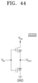
- FIG. 44 is a circuit diagram of a ternary inverter according to example embodiments.
- FIG. 45 is a flowchart of a method of manufacturing a ternary inverter according to an example embodiment.
- FIGS. 46 to 51 are perspective views for describing a method of manufacturing the ternary inverter of FIG. 45 .
- FIG. 52 is a gate voltage-drain current graph of ternary inverters of the present disclosure and binary inverters.
- FIG. 53 is a graph showing an input voltage Vin-output voltage Vout of a ternary inverter of the present disclosure and a binary inverter.
- FIG. 54 is a flowchart of a method of manufacturing a transistor according to an example embodiment.
- FIGS. 55 to 60 are cross-sectional views for describing the method of manufacturing a transistor of FIG. 54 .
- FIG. 61 is a flowchart of a method of manufacturing a ternary inverter according to an example embodiment.
- FIGS. 62 to 70 are cross-sectional views for describing the method of manufacturing a ternary inverter of FIG. 61 .
- a transistor includes a substrate; a pair of constant current forming regions provided in the substrate; a pair of source/drain regions respectively provided on the pair of constant current forming regions in the substrate; and a gate structure provided between the pair of source/drain regions, wherein any one of the constant current forming regions immediately adjacent to any one of the pair of source/drain regions serving as a drain forms a constant current between the any one of the pair of source/drain region serving as the drain and the any one of the constant current forming regions.
- a ternary inverter includes an NMOS transistor and a PMOS transistor, wherein the NMOS transistor and the PMOS transistor each includes a substrate, a pair of constant current forming regions provided in the substrate, and a source pattern and a drain region respectively provided on the pair of constant current forming regions, any one of the pair of constant current forming regions immediately adjacent to the drain region forms a constant current between the drain region and the any one of the pair of constant current forming regions, and the drain region of the NMOS transistor and the drain region of the PMOS transistor are electrically connected to each other and have the same voltage as each other.
- a method of manufacturing a transistor includes forming a gate structure on a substrate; forming a pair of etching regions on the substrate; forming a pair of constant current forming regions in the pair of etched regions, respectively; and forming a pair of source/drain regions on the pair of constant current forming regions, respectively, wherein the pair of etching regions are spaced apart from each other across the gate structure therebetween, and any one of the constant current forming regions immediately adjacent to any one of the pair of source/drain regions serving as a drain forms a constant current between the any one of the pair of source/drain region serving as the drain and the any one of the constant current forming regions.
- a method of manufacturing a transistor includes forming a fin structure extending in a first direction on a substrate; forming a gate structure extending in a second direction intersecting the first direction on the fin structure; and forming a source region and a drain region in the fin structure, wherein the fin structure includes a constant current forming fin and a channel layer sequentially stacked on the substrate, the source region and the drain region are formed on the channel layer and are spaced apart from each other across the gate electrode therebetween, and the constant current forming fin forms a constant current between the drain region and the substrate and is formed through an epitaxial growth process.
- a method of manufacturing a ternary inverter includes forming a first well region and a second well region different from each other in a substrate; forming a first fin structure and a second fin structure extending in a first direction on the first well region and the second well region, respectively; forming a gate structure extending in a second direction intersecting the first direction on the first fin structure and the second fin structure; and forming a source region and a drain region spaced apart from each other across the gate structure therebetween in each of the first fin structure and the second fin structure, wherein the first fin structure and the second fin structure include a first constant current forming fin and a second constant current forming fin, respectively, the first constant current forming fin forms a constant current between the drain region and the first well region of the first fin structure and is formed through an epitaxial growth process, and the second constant current forming fin forms a constant current between the drain region and the second well region of the second fin structure and is formed through an epitaxial growth process.
- a method of manufacturing a transistor includes forming a constant current forming layer on a substrate; forming a channel layer on the constant current forming layer; forming a gate electrode on the channel layer; and forming a source region and a drain region in the channel layer, wherein the source region and the drain region are spaced apart from each other across the gate electrode therebetween, and the constant current forming layer forms a constant current between the drain region and the substrate and is formed through an epitaxial growth process.
- FIG. 1 is a cross-sectional view of a transistor according to example embodiments.
- a transistor 10 may be provided.
- the transistor 10 may include a substrate 100 , a pair of device isolation regions ST, a pair of source/drain regions SD, a pair of constant current forming regions 200 , and a gate structure 300 .
- the substrate 100 may be a semiconductor substrate.
- the substrate 100 may include silicon (Si).
- the substrate 100 may have a first conductivity type.
- the first conductivity type may be n-type or p-type.
- the substrate 100 may include a group V element (e.g., P or As) as an impurity.
- the substrate 100 may include a group III element (e.g., B or In) as an impurity.
- the pair of device isolation regions ST may be provided on the substrate 100 .
- the pair of device isolation regions ST may be spaced apart from each other in a first direction DR 1 parallel to a top surface 100 u of the substrate 100 .
- the pair of device isolation regions ST may extend in a second direction DR 2 perpendicular to the top surface 100 u of the substrate 100 .
- the pair of device isolation regions ST may include an electrically insulating material.
- the pair of device isolation regions ST may include SiO 2 or a high-k material (e.g., SiON, HfO 2 , or ZrO 2 ).
- the pair of source/drain regions SD may be provided on the substrate 100 .
- the pair of source/drain regions SD may be spaced apart from each other in the first direction DR 1 .
- One of the pair of source/drain regions SD may be a source of the transistor 10 .
- the other one of the pair of source/drain regions SD may be a drain of the transistor 10 .
- the pair of source/drain regions SD may have a second conductivity type different from the first conductivity type.
- the pair of source/drain regions SD may include a group III element (e.g., B or In) as an impurity.
- the pair of source/drain regions SD may include a group V element (e.g., P or As) as an impurity.
- the pair of constant current forming regions 200 may be provided under the pair of source/drain regions SD, respectively.
- the pair of constant current forming regions 200 may respectively overlap the pair of source/drain regions SD in the second direction DR 2 .
- the pair of constant current forming regions 200 may be electrically connected to the pair of source/drain regions SD.
- the pair of constant current forming regions 200 may directly contact the pair of source/drain regions SD.
- the pair of constant current forming regions 200 may be spaced apart from each other in the first direction DR 1 .
- the pair of constant current forming regions 200 may have the first conductivity type.
- the pair of constant current forming regions 200 may include a group V element (e.g., P or As) as an impurity.
- the pair of constant current forming regions 200 may include a group III element (e.g., B or In) as an impurity.
- the doping concentration of the pair of constant current forming regions 200 may be higher than that of the substrate 100 .
- the doping concentration of the pair of constant current forming regions 200 may be 3 ⁇ 10 18 cm ⁇ 3 or higher.
- An electric field may be formed between the pair of constant current forming regions 200 and the pair of source/drain regions SD.
- the intensity of the electric field may be 10 6 V/cm or higher.
- the gate structure 300 may be provided on the substrate 100 .
- the gate structure 300 may include a gate insulation layer 310 , a gate electrode 320 , and a pair of spacers 330 .
- the gate electrode 320 may include an electrically conductive material.
- the gate electrode 320 may include a doped semiconductor material, a metal, an alloy, or a combination thereof.
- the gate electrode 320 may include doped polysilicon, tungsten (W), titanium nitride (TiN), or a combination thereof.
- the gate insulation layer 310 may be provided between the gate electrode 320 and the substrate 100 .
- the gate insulation layer 310 may electrically insulate the gate electrode 320 and the substrate 100 from each other.
- the gate insulation layer 310 may include an electrically insulating material.
- the gate insulation layer 310 may include at least one material selected from among silicon oxide, silicon nitride, silicon oxynitride, oxide/nitride/oxide (ONO), and a high-k material.
- the gate insulation layer 310 may include a material having a dielectric constant from about 10 to about 25.
- the gate insulation layer 310 may include at least one material selected from among hafnium oxide (HfO), hafnium silicon oxide (HfSiO), hafnium oxynitride (HfON), hafnium silicon oxynitride (HfSiON), lanthanum oxide (LaO), lanthanum aluminum oxide (LaAlO), zirconium oxide (ZrO), zirconium silicon oxide (ZrSiO), zirconium oxynitride (ZrON), zirconium silicon oxynitride (ZrSiON), tantalum oxide (TaO), titanium oxide (TiO), barium strontium titanium oxide (BaSrTiO), barium titanium oxide (BaTiO), strontium titanium oxide (SrTiO), yttrium oxide (YO), aluminum oxide (AlO), and lead scandium tantalum oxide (PbScTaO).
- hafnium oxide HfO
- the pair of spacers 330 may be provided on both sidewalls of the gate electrode 320 , respectively.
- the pair of spacers 330 may extend onto the both sidewalls of the gate insulation layer 310 , respectively.
- the pair of spacers 330 may include an electrically insulating material.
- the pair of spacers 330 may include SiO 2 or a high-k material (e.g., SiON, HfO 2 , or ZrO 2 ).
- the threshold voltage of the transistor 10 may be adjusted by a doping concentration of the substrate 100 and/or a work function of the gate electrode 320 .
- the work function of the gate electrode 320 may be controlled by the material constituting the gate electrode 320 or by an additional work function control layer (not shown).
- the additional work function control layer may be disposed between the gate insulation layer 310 and the substrate 100 .
- any one of the pair of constant current forming regions 200 immediately adjacent to any one of the pair of source/drain regions SD serving as the drain may form a constant current between a source/drain region SD serving as the drain and a constant current forming region 200 immediately adjacent thereto.
- the constant current may be a band-to-band tunneling (BTBT) current between the source/drain region SD serving as the drain and the constant current forming region 200 immediately adjacent thereto.
- the constant current may be independent from a gate voltage applied to the gate electrode 320 . In other words, the constant current may flow regardless of the gate voltage.
- the transistor 10 is an NMOS transistor
- a constant current may flow to the substrate 100 from the source/drain region SD serving as the drain through the constant current forming region 200 immediately adjacent thereto.
- the transistor 10 is a PMOS transistor
- a constant current may flow from the substrate 100 to the source/drain region SD serving as the drain through the constant current forming region 200 immediately adjacent to the source/drain region SD serving as the drain.
- the present disclosure may provide the transistor 10 in which a constant current is formed between any one of the pair of source/drain regions SD serving as the drain and the constant current forming region 200 immediately adjacent thereto.
- FIG. 2 shows gate voltage-drain current graphs of NMOS transistors according to the present disclosure and conventional NMOS transistors.
- gate voltage-drain current graphs NGR 1 and NGR 2 of conventional NMOS transistors and gate voltage-drain current graphs NGR 3 , NGR 4 , and NGR 5 of NMOS transistors according to the present disclosure are shown.
- Drain currents of the conventional NMOS transistors do not have a constant current component that flows regardless of a gate voltage.
- Drain currents of the NMOS transistors of the present disclosure have a constant current component that flows regardless of a gate voltage. For example, even when the NMOS transistors of the present disclosure are in an OFF state, a constant current flows through the NMOS transistors of the present disclosure.
- FIG. 3 shows gate voltage-drain current graphs of PMOS transistors according to the present disclosure and conventional PMOS transistors.
- gate voltage-drain current graphs PGR 1 and PGR 2 of conventional PMOS transistors and gate voltage-drain current graphs PGR 3 , PGR 4 , and PGR 5 of PMOS transistors of the present disclosure are shown.
- Drain currents of the conventional PMOS transistors do not have a constant current component that flows regardless of a gate voltage.
- Drain currents of the PMOS transistors of the present disclosure have a constant current component that flows regardless of a gate voltage. For example, even when the PMOS transistors of the present disclosure are in an OFF state, a constant current flows through the PMOS transistors of the present disclosure.
- FIG. 4 is a flowchart of a method of manufacturing the transistor of FIG. 1 according to an example embodiment.
- FIGS. 5 to 7 are cross-sectional views for describing the method of manufacturing a transistor of FIG. 4 .
- the substrate 100 may be a semiconductor substrate.
- the substrate 100 may include silicon (Si).
- the substrate 100 may have a first conductivity type.
- the first conductivity type may be n-type or p-type.
- the substrate 100 may include a group V element (e.g., P or As) as an impurity.
- the substrate 100 may include a group III element (e.g., B or In) as an impurity.
- the pair of device isolation regions ST may be formed in the substrate 100 .
- a process of forming the pair of device isolation regions ST may include recessing the substrate 100 to a partial depth and filling a recessed region with an electrically insulating material.
- the substrate 100 may recessed by performing an anisotropic etching process on the substrate 100 .
- the electrically insulating material may be provided to a pair of recessed regions through a chemical vapor deposition process or a physical vapor deposition process.
- the electrically insulating material may include SiO 2 or a high-k material (e.g., SiON, HfO 2 , or ZrO 2 ).
- the gate structure 300 may be formed on the substrate 100 (operation S 120 ).
- the gate structure 300 may include the gate insulation layer 310 and the gate electrode 320 that are sequentially stacked and may include the pair of spacers 330 covering side surfaces of the gate insulation layer 310 and the gate electrode 320 .
- a process of forming the gate insulation layer 310 and the gate electrode 320 may include sequentially depositing an electrically insulating film and an electrically conductive film on the substrate 100 and patterning the electrically conductive film and the electrically insulating film.
- the electrically insulating film may include at least one material selected from among silicon oxide, silicon nitride, silicon oxynitride, oxide/nitride/oxide (ONO), and a high-k material.
- the electrically insulating film may include a material having a dielectric constant from about 10 to about 25.
- the electrically insulating film may include at least one material selected from among hafnium oxide (HfO), hafnium silicon oxide (HfSiO), hafnium oxynitride (HfON), hafnium silicon oxynitride (HfSiON), lanthanum oxide (LaO), lanthanum aluminum oxide (LaAlO), zirconium oxide (ZrO), zirconium silicon oxide (ZrSiO), zirconium oxynitride (ZrON), zirconium silicon oxynitride (ZrSiON), tantalum oxide (TaO), titanium oxide (TO), barium strontium titanium oxide (BaSrTiO), barium titanium oxide (BaTiO), strontium titanium oxide (SrTiO), yttrium oxide (YO), aluminum oxide (AlO), and lead scandium tantalum oxide (PbScTaO).
- hafnium oxide HfO
- hafnium silicon oxide
- the electrically conductive film may include a doped semiconductor material, a metal, an alloy, or a combination thereof.
- the electrically conductive film may include doped polysilicon, tungsten (W), titanium nitride (TiN), or a combination thereof.
- a process of forming the pair of spacers 330 may include forming an electrically insulating film extending along surfaces of the pair of device isolation regions ST, the substrate 100 , the gate insulation layer 310 , and the gate electrode 320 and performing a large-area anisotropic etching process to remove a portion of the electrically insulating film. After an etching process is finished, the gate insulation layer 310 and the electrically insulating film on the side surfaces of the gate electrode 320 may remain.
- the electrically insulating film may include SnO 2 or a high-k material (e.g., SiON, HfO 2 , or ZrO 2 ).
- the pair of constant current forming regions 200 may be formed on the substrate 100 (operation S 130 ).
- a process of forming the pair of constant current forming regions 200 may include performing an ion implantation process II.
- the pair of constant current forming regions 200 may have the same conductivity type as that of the substrate 100 .
- a group V element e.g., P or As
- P or As may be further implanted into the substrate 100 to form a pair of n-type constant current forming regions 200 .
- a group III element e.g., B or In
- the doping concentration of the pair of constant current forming regions 200 may be higher than that of the substrate 100 .
- the doping concentration of the pair of constant current forming regions 200 may be 3 ⁇ 10 18 cm ⁇ 3 or higher.
- the pair of source/drain regions SD may be respectively formed on the pair of constant current forming regions 200 (operation S 140 ).
- a process of forming the pair of source/drain regions SD may include performing a process of doping a portion of the substrate 100 between a spacer 330 and a device isolation region ST immediately adjacent to each other.
- a doping process may include an ion implantation process.
- the pair of source/drain regions SD may have a conductivity type different from that of the pair of constant current forming regions 200 .
- a group III element e.g., B or In
- a group V element e.g., P or As
- the pair of source/drain regions SD may be formed to overlap the pair of constant current forming regions 200 in the second direction DR 2 .
- the pair of source/drain regions SD may be electrically connected to the pair of constant current forming regions 200 .
- the pair of source/drain regions SD may directly contact the pair of constant current forming regions 200 .
- the substrate 100 may be heat-treated.
- the thermal budget of a heat treatment process may affect the threshold voltage characteristics and the constant current of the transistor 10 .
- impurities implanted into the upper portion of the substrate 100 may diffuse into a channel and change the threshold voltage.
- the thermal budget is larger than demanded, the doping concentration between the pair of source/drain regions SD and the pair of constant current forming regions 200 may be gently changed, and thus the magnitude of the constant current may be reduced.
- the thermal budget may be adjusted to prevent or minimize the threshold voltage characteristic of the transistor 10 from being changed.
- the thermal budget may be adjusted, such that the transistor 10 has a demanded constant current.
- the present disclosure may provide a method of manufacturing the transistor 10 in which a constant current flows between any one of the pair of source/drain regions SD serving as the drain and the constant current forming region 200 immediately adjacent thereto.
- FIG. 8 is a flowchart of a method of manufacturing the transistor of FIG. 1 according to an example embodiment.
- FIGS. 9 and 10 are cross-sectional views for describing the method of manufacturing a transistor of FIG. 8 .
- descriptions substantially identical to those given above with reference to FIGS. 4 to 7 may not be given.
- the pair of device regions ST may be formed on the substrate 100 (operation S 210 ).
- a process of forming the pair of device regions ST on the substrate 100 may be substantially identical to that described with reference to FIGS. 4 and 5 .
- the gate structure 300 may be formed on the substrate 100 (operation S 220 ).
- a process of forming the gate structure 300 on the substrate 100 may be substantially identical to that described with reference to FIGS. 4 and 6 .
- the upper portion of the substrate 100 may be etched to form a pair of recessed regions RR (operation S 230 ).
- a process of forming the pair of recessed regions RR may include performing an anisotropic etching process on the substrate 100 by using an etching mask provided on the substrate 100 .
- the pair of recessed regions RR may be spaced apart from each other across the gate structure 300 therebetween.
- the etching mask may be removed during or after an etching process.
- the pair of constant current forming regions 200 may be respectively formed in the pair of recessed regions RR (operation S 240 ).
- the pair of constant current forming regions 200 may be formed through an epitaxy growth process.
- the pair of constant current forming regions 200 may include silicon (Si).
- the pair of constant current forming regions 200 may have the first conductivity type.
- the conductivity type of the pair of constant current forming regions 200 is n-type
- the pair of constant current forming regions 200 may include a group V element (e.g., P or As) as an impurity.
- the pair of constant current forming regions 200 may include a group III element (e.g., B or In) as an impurity.
- the doping concentration of the pair of constant current forming regions 200 may be higher than that of the substrate 100 .
- the doping concentration of the pair of constant current forming regions 200 may be 3 ⁇ 10 18 cm ⁇ 3 or higher.
- the pair of source/drain regions SD may be respectively formed on the pair of constant current forming regions 200 (operation S 250 ).
- the pair of source/drain regions SD may be formed through an epitaxial growth process.
- the pair of source/drain regions SD may include silicon (Si).
- the pair of source/drain regions SD may have the second conductivity type.
- the pair of constant current forming regions 200 may include a group V element (e.g., P or As) as an impurity.
- the conductivity type of the pair of constant current forming regions 200 is p-type
- the pair of constant current forming regions 200 may include a group III element (e.g., B or In) as an impurity.
- the present disclosure may provide a method of manufacturing the transistor 10 in which a constant current flows between any one of the pair of source/drain regions SD serving as the drain and the constant current forming region 200 immediately adjacent thereto.
- FIG. 11 is a perspective view of a transistor according to an example embodiment.
- FIG. 12 shows cross-sectional views taken along lines I-I′ and II-II′ of FIG. 11 .
- a transistor 20 may be provided.
- the transistor 10 may include the substrate 100 , a fin structure FS, a pair of lower insulation layers 110 , and the gate structure 300 .
- the substrate 100 may be a semiconductor substrate.
- the substrate 100 may include silicon (Si).
- the substrate 100 may have a first conductivity type.
- the first conductivity type may be n-type or p-type.
- the substrate 100 may include a group V element (e.g., P or As) as an impurity.
- the substrate 100 may include a group III element (e.g., B or In) as an impurity.
- the fin structure FS may be provided on the substrate 100 .
- the fin structure FS may include a lower semiconductor region LSR, the pair of constant current forming regions 200 , the pair of source/drain regions SD, and a channel region CR.
- the lower semiconductor region LSR may be provided under the fin structure FS.
- the lower semiconductor region LSR may extend in the second direction DR 2 parallel to the top surface 100 u of the substrate 100 .
- the lower semiconductor region LSR may protrude from the top surface 100 u of the substrate 100 .
- the lower semiconductor region LSR may include silicon (Si).
- the lower semiconductor region LSR may have the first conductivity type.
- the lower semiconductor region LSR may include a group V element (e.g., P or As) as an impurity.
- the conductivity type of the lower semiconductor region LSR is p-type, the lower semiconductor region LSR may include a group III element (e.g., B or In) as an impurity.
- the pair of constant current forming regions 200 may be provided on the lower semiconductor region LSR.
- the pair of constant current forming regions 200 may be spaced apart from each other across the gate structure 300 therebetween.
- the pair of constant current forming regions 200 may be spaced apart from each other in the second direction DR 2 .
- the pair of constant current forming regions 200 may include silicon (Si).
- the pair of constant current forming regions 200 may have the first conductivity type.
- the pair of constant current forming regions 200 may include a group V element (e.g., P or As) as an impurity.
- the pair of constant current forming regions 200 may include a group III element (e.g., B or In) as an impurity.
- the doping concentration of the pair of constant current forming regions 200 may be higher than those of the substrate 100 and the lower semiconductor region LSR.
- the doping concentration of the pair of constant current forming regions 200 may be 3 ⁇ 10 18 cm ⁇ 3 or higher.
- the pair of source/drain regions SD may be respectively provided on the pair of constant current forming regions 200 .
- the pair of source/drain regions SD may be spaced apart from each other across the gate structure 300 therebetween.
- the pair of source/drain regions SD may be spaced apart from each other in the second direction DR 2 .
- One of the pair of source/drain regions SD may be a source of the transistor 20 .
- the other one of the pair of source/drain regions SD may be a drain of the transistor 20 .
- the pair of source/drain regions SD may have the second conductivity type different from the first conductivity type.
- the pair of source/drain regions SD may include a group III element (e.g., B or In) as an impurity.
- the pair of source/drain regions SD may include a group V element (e.g., P or As) as an impurity.
- the pair of source/drain regions SD may be electrically connected to the pair of constant current forming regions 200 .
- the pair of source/drain regions SD may directly contact the pair of constant current forming regions 200 .
- An electric field may be formed between the pair of constant current forming regions 200 and the pair of source/drain regions SD.
- the intensity of the electric field may be 10 6 V/cm or higher.
- the channel region CR may be provided on the lower semiconductor region LSR.
- the channel region CR may extend from the lower semiconductor region LSR to a region between the pair of source/drain regions SD.
- the channel region CR may be provided between the pair of constant current forming regions 200 and between the pair of source/drain regions SD.
- the channel region CR may include silicon (Si).
- the channel region CR may have the first conductivity type. When the conductivity type of the channel region CR is n-type, the channel region CR may include a group V element (e.g., P or As) as an impurity. When the conductivity type of the channel region CR is p-type, the channel region CR may include a group III element (e.g., B or In) as an impurity.
- the doping concentration of the channel region CR may be lower than that of the pair of constant current forming regions 200 .
- the doping concentration of the channel region CR may be substantially identical to that of the lower semiconductor region LSR.
- the channel region CR may be a region in which a channel of the transistor 20 is formed.
- the pair of lower insulation layers 110 may be spaced apart from each other across the fin structure FS therebetween.
- the pair of lower insulation layers 110 may be spaced apart from each other in the first direction DR 1 that is parallel to the top surface 100 u of the substrate 100 and intersects the second direction DR 2 .
- the pair of lower insulation layers 110 may overlap the lower semiconductor region LSR in the first direction DR 1 .
- the pair of lower insulation layers 110 may include an electrically insulating material.
- the pair of lower insulation layers 110 may include SiO 2 or a high-k material (e.g., SiON, HfO 2 , or ZrO 2 ).
- the gate structure 300 may be provided on the fin structure FS and the pair of lower insulation layers 110 .
- the gate structure 300 may include the gate insulation layer 310 and the gate electrode 320 that are sequentially stacked.
- the gate structure 300 may extend in the first direction DR 1 .
- the gate structure 300 may overlap the channel region CR in a third direction DR 3 .
- the gate structure 300 may extend along surfaces of the pair of lower insulation layers 110 and a channel fin 220 .
- the gate insulation layer 310 may include an electrically insulating material.
- the gate insulation layer 310 may include at least one material selected from among silicon oxide, silicon nitride, silicon oxynitride, oxide/nitride/oxide (ONO), and a high-k material.
- the gate insulation layer 310 may include a material having a dielectric constant from about 10 to about 25.
- the gate insulation layer 310 may include at least one material selected from among hafnium oxide (HfO), hafnium silicon oxide (HfSiO), hafnium oxynitride (HfON), hafnium silicon oxynitride (HfSiON), lanthanum oxide (LaO), lanthanum aluminum oxide (LaAlO), zirconium oxide (ZrO), zirconium silicon oxide (ZrSiO), zirconium oxynitride (ZrON), zirconium silicon oxynitride (ZrSiON), tantalum oxide (TaO), titanium oxide (TIO), barium strontium titanium oxide (BaSrTiO), barium titanium oxide (BaTiO), strontium titanium oxide (SrTiO), yttrium oxide (YO), aluminum oxide (AlO), and lead scandium tanta
- the gate electrode 320 may include an electrically conductive material.
- the gate electrode 320 may include a doped semiconductor material, a metal, an alloy, or a combination thereof.
- the gate electrode 320 may include doped polysilicon, tungsten (W), titanium nitride (TiN), or a combination thereof.
- the threshold voltage of the transistor 20 may be adjusted by a doping concentration of the channel region CR and/or the work function of the gate electrode 320 .
- the work function of the gate electrode 320 may be controlled by the material constituting the gate electrode 320 or by an additional work function control layer (not shown).
- the additional work function control layer may be disposed between the gate insulation layer 310 and the channel region CR.
- the constant current forming region 200 immediately adjacent to the source/drain region SD serving as the drain of the transistor 20 from between the pair of source/drain regions SD may form a constant current between the source/drain region SD serving as the drain and the constant current forming region 200 .
- the constant current may be a band-to-band tunneling (BTBT) current between the source/drain region SD serving as the drain and the constant current forming region 200 immediately adjacent thereto.
- the constant current may be independent from a gate voltage applied to the gate electrode 320 . In other words, the constant current may flow regardless of the gate voltage.
- a constant current may flow to the lower semiconductor region LSR and the substrate 100 from the source/drain region SD serving as the drain through the constant current forming region 200 immediately adjacent thereto.
- a constant current may flow to the source/drain region SD serving as the drain from the substrate 100 through the lower semiconductor region LSR and the constant current forming region 200 immediately adjacent to the source/drain region SD serving as the drain.
- the present disclosure may provide the transistor 20 in which a constant current flows between the source/drain region SD serving as the drain and the constant current forming region 200 immediately adjacent thereto.
- FIG. 13 is a flowchart of a method of manufacturing the transistor of FIG. 11 according to an example embodiment.
- FIGS. 14 , 16 , 18 , and 20 are perspective views for describing the method of manufacturing a transistor of FIG. 13 .
- FIGS. 15 , 17 , 19 , and 21 are cross-sectional views taken along lines I-I′ and II-II′ of FIGS. 14 , 16 , 18 , and 20 , respectively.
- the fin structure FS may be formed on the substrate 100 (operation S 310 ).
- a process of forming the fin structure FS may include preparing a semiconductor film (not shown) and exposing the fin structure FS by patterning the upper portion of the semiconductor film.
- the semiconductor film may be, for example, a silicon (Si) film.
- the semiconductor film may have the first conductivity type.
- the first conductivity type may be n-type or p-type.
- the semiconductor film may include a group V element (e.g., P or As) as an impurity.
- the semiconductor film may include a group III element (e.g., B or In) as an impurity.
- a patterning process may include forming a mask pattern on the semiconductor film and performing an anisotropic etching process by using the mask pattern as an etching mask on the semiconductor film.
- the mask pattern may be removed during or after the anisotropic etching process.
- the pair of lower insulation layers 110 may be formed on the substrate 100 (operation S 320 ).
- a process of forming the pair of lower insulation layers 110 may include a process of forming a deposition film (not shown) by depositing an electrically insulating material on the substrate 100 and a process of exposing the upper portion of the fin structure FS by etching the deposition film.
- a deposition process may include a chemical vapor deposition process or a physical vapor deposition process.
- the electrically insulating material may include SiO 2 or a high-k material (e.g., SiON, HfO 2 , or ZrO 2 ).
- the gate structure 300 may be formed on the fin structure FS (operation S 330 ).
- a process of forming the gate structure 300 may include a process of sequentially depositing an electrically insulating material and an electrically conductive material on the pair of lower insulation layers 110 and the fin structure FS and a process of patterning the electrically insulating material and the electrically conductive material.
- a deposition process may include a chemical vapor deposition (CVD) process, a physical vapor deposition (PVD) process, or an atomic layer deposition (ALD) process.
- the electrically insulating material may include at least one material selected from among silicon oxide, silicon nitride, silicon oxynitride, oxide/nitride/oxide (ONO), and a high-k material.
- the electrically insulating material may include a material having a dielectric constant from about 10 to about 25.
- the electrically insulating material may include at least one material selected from among hafnium oxide (HfO), hafnium silicon oxide (HfSiO), hafnium oxynitride (HfON), hafnium silicon oxynitride (HfSiON), lanthanum oxide (LaO), lanthanum aluminum oxide (LaAlO), zirconium oxide (ZrO), zirconium silicon oxide (ZrSiO), zirconium oxynitride (ZrON), zirconium silicon oxynitride (ZrSiON), tantalum oxide (TaO), titanium oxide (TiO), barium strontium titanium oxide (BaSrTiO), barium titanium oxide (BaTiO), strontium titanium oxide (SrTiO), yttrium oxide (YO), aluminum oxide (AlO), and lead scandium tantalum oxide (PbScTaO).
- hafnium oxide HfO
- the electrically conductive material may include a doped semiconductor material, a metal, an alloy, or a combination thereof.
- the electrically conductive material may include doped polysilicon, tungsten (W), titanium nitride (TIN), or a combination thereof.
- the pair of constant current forming regions 200 may be formed in the fin structure FS (operation S 340 ).
- a process of forming the pair of constant current forming regions 200 may include a process of doping the fin structure FS on sidewalls of the gate structure 300 .
- the pair of constant current forming regions 200 may have the same conductivity type as that of the fin structure FS.
- a group V element e.g., P or As
- P or As may be further implanted into the fin structure FS to form a pair of n-type constant current forming regions 200 .
- a group III element e.g., B or In
- the doping concentration of the pair of constant current forming regions 200 may be higher than that of the fin structure FS.
- the doping concentration of the pair of constant current forming regions 200 may be 3 ⁇ 10 18 cm ⁇ 3 or higher.
- the pair of source/drain regions SD may be respectively formed in portions of the fin structure FS exposed on both side surfaces of the gate structure 300 (operation S 350 ).
- a process of forming the pair of source/drain regions SD may include a process of doping the portions of the fin structure FS exposed on both side surfaces of the gate structure 300 .
- a doping process may include an ion implantation process.
- the pair of source/drain regions SD may have the second conductivity type different from the first conductivity type. When the first conductivity type is p-type, the second conductivity type may be n-type.
- group V elements e.g., P or As
- the first conductivity type is n-type
- the second conductivity type may be p-type
- a group III element e.g., B or In
- One of the pair of source/drain regions SD may be a source of the transistor 20 , and the other one may be a drain of the transistor 20 .
- the fin structure FS may be heat-treated.
- the thermal budget of a heat treatment process may affect the threshold voltage characteristics and the constant current of the transistor 20 .
- impurities implanted into the fin structure FS may diffuse into a channel and change the threshold voltage.
- the thermal budget is larger than demanded, the doping concentration between the pair of source/drain regions SD and the pair of constant current forming regions 200 may be gently changed, and thus the magnitude of the constant current may be reduced.
- the thermal budget may be adjusted to prevent or minimize the threshold voltage characteristic of the transistor 20 from being changed. The thermal budget may be adjusted, such that the transistor 20 has a demanded constant current.
- the present disclosure may provide a method of manufacturing the transistor 20 in which a constant current flows between the source/drain region SD serving as the drain and the constant current forming region 200 immediately adjacent thereto.
- FIG. 22 is a flowchart of a method of manufacturing the transistor of FIG. 11 according to an example embodiment.
- FIGS. 23 and 25 are perspective views for describing the method of manufacturing a transistor of FIG. 22 .
- FIGS. 24 and 26 are cross-sectional views taken along lines I-I′ and II-II′ of FIGS. 23 and 25 , respectively.
- descriptions substantially identical to those given above with reference to FIGS. 13 to 21 may not be given.
- the fin structure FS may be formed on the substrate 100 (operation S 410 ).
- a process of forming the fin structure FS may be substantially identical to that described with reference to FIGS. 13 to 15 .
- the pair of lower insulation layers 110 may be formed on both side surfaces of the fin structure FS (operation S 420 ).
- a process of forming the pair of lower insulation layers 110 may be substantially identical to that described with reference to FIGS. 13 , 16 , and 17 .
- the gate structure 300 may be formed on the fin structure FS (operation S 430 ).
- a process of forming the gate structure 300 may be substantially identical to that described with reference to FIGS. 13 , 18 , and 19 .
- the upper portion of the fin structure FS may be removed on both side surfaces of the gate structure 300 (operation S 440 ).
- a process of removing the upper portion of the fin structure FS may include performing an etching process by using a mask pattern (not shown). As the upper portion of the fin structure FS is removed, both side surfaces CRs of the channel region CR may be exposed. In an embodiment, an etching process of removing the upper portion of the fin structure FS may be performed, such that the top surface LSRu of the lower semiconductor region LSR on the both side surfaces CRs of the channel region CR has a height lower than that of the top surfaces of the pair of lower insulation layers 110 .
- the height of the top surface LSRu of the lower semiconductor region LSR is not limited to be lower than the height of the top surfaces of the pair of lower insulation layers 110 .
- the top surface LSRu of the lower semiconductor region LSR may be placed at the same height as or higher than the top surfaces of the pair of lower insulation layers 110 .
- the pair of constant current forming regions 200 may be formed on the top surface LSRu of the lower semiconductor region LSR on both side surfaces CRs of the channel region CR (operation S 450 ).
- the pair of constant current forming regions 200 may be formed through an epitaxy growth process.
- the pair of constant current forming regions 200 may be an epitaxial layer.
- the pair of constant current forming regions 200 may include silicon (Si).
- the pair of constant current forming regions 200 may have the first conductivity type.
- the pair of constant current forming regions 200 may include a group V element (e.g., P or As) as an impurity.
- the pair of constant current forming regions 200 may include a group III element (e.g., B or In) as an impurity.
- the doping concentration of the pair of constant current forming regions 200 may be higher than that of the substrate 100 .
- the doping concentration of the pair of constant current forming regions 200 may be 3 ⁇ 10 18 cm ⁇ 3 or higher.
- the pair of source/drain regions SD may be respectively formed on the pair of constant current forming regions 200 (operation S 460 ).
- the pair of source/drain regions SD may be formed through an epitaxial growth process.
- the pair of source/drain regions SD may be an epitaxial layer.
- the pair of source/drain regions SD may include silicon (Si).
- the pair of source/drain regions SD may have the second conductivity type different from the first conductivity type.
- the pair of source/drain regions SD may include a group III element (e.g., B or In) as an impurity.
- the pair of source/drain regions SD may include a group V element (e.g., P or As) as an impurity.
- the impurities may be implanted into the pair of source/drain regions SD through an in-situ process when an epitaxial growth process is performed.
- the present disclosure may provide a method of manufacturing the transistor 20 in which a constant current flows between the source/drain region SD serving as the drain and the constant current forming region 200 immediately adjacent thereto.
- FIG. 27 is a circuit diagram of a ternary inverter according to example embodiments. For brevity of description, descriptions substantially identical to those given above with reference to FIGS. 1 and 11 may not be given.
- a ternary inverter 30 including an NMOS transistor and a PMOS transistor may be provided.
- the NMOS transistor may be the transistor 10 described with reference to FIG. 1 having a p-type substrate, a pair of p-type constant current forming regions, and a pair of n-type source/drain regions.
- the PMOS transistor may be the transistor 10 described with reference to FIG. 1 having an n-type substrate, a pair of n-type constant current forming regions, and a pair of p-type source/drain regions.
- the NMOS transistor may be the transistor 20 described with reference to FIG. 11 having a p-type substrate, a pair of p-type constant current forming regions, and a pair of n-type source/drain regions.
- the PMOS transistor may be the transistor 20 described with reference to FIG. 1 having an n-type substrate, a pair of n-type constant current forming regions, and a pair of p-type source/drain regions.
- a ground voltage may be applied to the source and the substrate of the NMOS transistor.
- V 0 volts
- a driving voltage V DD may be applied to the source and the substrate of the PMOS transistor.
- An input voltage Vin may be applied to each of a gate electrode of the NMOS transistor and a gate electrode of the PMOS transistor.
- a drain of the NMOS transistor may be electrically connected to a drain of the PMOS transistor and may have the same voltage.
- the voltage of the drain of the NMOS transistor and the drain of the PMOS transistor may be an output voltage Vout of the ternary inverter 30 .
- a constant current may flow from the drain of the NMOS transistor to the substrate of the NMOS transistor.
- a constant current may flow from the substrate of the PMOS transistor to the drain of the PMOS transistor.
- the constant currents may be independent of the input voltage Vin.
- a first input voltage may be applied to the gate electrode of the PMOS transistor and the gate electrode of the NMOS transistor, such that the PMOS transistor has a constant current dominant over a channel current and the NMOS transistor has a channel current dominant over a constant current.
- the output voltage Vout of the ternary inverter 30 may be a first voltage.
- a second input voltage may be applied to the gate electrode of the NMOS transistor and the gate electrode of the PMOS transistor, such that the NMOS transistor has a constant current dominant over a channel current and the PMOS transistor has a channel current dominant over a constant current.
- the output voltage of the ternary inverter 30 may be a second voltage greater than the first voltage.
- a third input voltage may be applied to the gate electrode of the PMOS transistor and the gate electrode of the NMOS transistor, such that each of the NMOS transistor and the PMOS transistor has a constant current that is dominant over the channel current.
- the output voltage of the ternary inverter 30 may be a third voltage between the first voltage and the second voltage.
- the constant current flowing from the drain of the NMOS transistor to the substrate of the NMOS transistor and the constant current flowing from the substrate of the PMOS transistor to the drain of the PMOS transistor may flow regardless of gate voltages applied to the gate electrodes of the PMOS transistor and the NMOS transistor.
- a current in the ternary inverter 30 may flow from the substrate of the PMOS transistor to the substrate of the NMOS transistor through the drain of the PMOS transistor and the drain of the NMOS transistor.
- the driving voltage VW applied to the substrate of the PMOS transistor may be distributed to a resistor between the substrate of the PMOS transistor and the drain of the PMOS transistor and a resistor between the substrate of the NMOS transistor and the drain of the NMOS transistor.
- the output voltage Vout may be a voltage applied to the resistor between the substrate of the NMOS transistor and the drain of the NMOS transistor.
- the output voltage Vout may have a value between the driving voltage V DD and 0 V.
- the output voltage Vout may have a state of 0 V (‘0’ state), a state of a voltage between the driving voltage V DD and 0 V (‘1’ state), or a state of the driving voltage VW (‘2’ state) according to the input voltage Vin.
- the present disclosure may provide a ternary inverter having three states according to the input voltage Vin.
- FIG. 28 is a gate voltage-drain current graph of ternary inverters of the present disclosure and binary inverters.
- gate voltage-drain current graphs IGR 1 and IGR 2 of binary inverters and gate voltage-drain current graphs IGR 3 , IGR 4 , and IGR 5 of ternary inverters of the present disclosure are shown.
- Drain currents of binary inverters do not have a constant current component that flows regardless of a gate voltage.
- Drain currents of the ternary inverters of the present disclosure have a constant current component that flows regardless of a gate voltage. For example, even when the ternary inverters of the present disclosure are in an OFF state, a constant current flows through the ternary inverters of the present disclosure.
- FIG. 29 is a graph showing an input voltage Vin-output voltage Vout of a ternary inverter of the present disclosure and a binary inverter.
- the driving voltage V DD of the ternary inverter of the present disclosure and the binary inverter was 1.0 V, and the ground voltage GND was 0 V.
- the input voltage Vin of the ternary inverter and the binary inverter was from 0 V to 1.0 V.
- the binary inverter when the input voltage was changed from 0 V to 1 V, the output voltage Vout rapidly decreased from 1 V to 0 V when the input voltage was nearby 0.5 V. In other words, the binary inverter had two states (e.g., a ‘0’ state and a ‘1’ state).
- the ternary inverter of the present disclosure when the input voltage was changed from 0 V to 1 V, the output voltage Vout rapidly decreased from 1 V to 0.5 V, maintained 0.5 V, and then rapidly decreased from 0.5 V to 0 V again.
- the ternary inverter of the present disclosure had three states (e.g., a ‘0’ state, a ‘1’ state, and a ‘2’ state).
- FIG. 30 is a flowchart of a method of manufacturing a transistor according to an example embodiment.
- FIGS. 31 , 32 , 33 , 34 , 35 , and 37 are perspective views for describing the method of manufacturing the transistor of FIG. 1 .
- FIGS. 36 and 38 are cross-sectional views taken along lines I-I′ and II-II′ of FIGS. 35 and 37 , respectively.
- a preliminary constant current forming layer 2210 p may be formed on a substrate 2100 (operation S 2110 ).
- the substrate 2100 may be a semiconductor substrate.
- the substrate 2100 may include silicon (Si).
- the substrate 2100 may have the first conductivity type.
- the first conductivity type may be n-type or p-type.
- the substrate 2100 may include a group V element (e.g., P or As) as an impurity.
- the substrate 2100 may include a group III element (e.g., B or In) as an impurity.
- the preliminary constant current forming layer 2210 p may be formed through an epitaxy growth process.
- the preliminary constant current forming layer 2210 p may be an epitaxial layer.
- the preliminary constant current forming layer 2210 p may include silicon (Si).
- the preliminary constant current forming layer 2210 p may have the first conductivity type.
- the conductivity type of the preliminary constant current forming layer 2210 p is n-type
- the preliminary constant current forming layer 2210 p may include a group V element (e.g., P or As) as an impurity.
- the conductivity type of the preliminary constant current forming layer 2210 p is p-type
- the preliminary constant current forming layer 2210 p may include a group III element (e.g., B or In) as an impurity.
- the doping concentration of the preliminary constant current forming layer 2210 p may be higher than that of the substrate 2100 .
- the doping concentration of the preliminary constant current forming layer 2210 p may be 3 ⁇ 10 18 cm ⁇ 3 or higher.
- the preliminary constant current forming layer 2210 p may be patterned, thereby forming a constant current forming fin 2210 (operation S 2120 ).
- the preliminary constant current forming layer 2210 p may be patterned through an anisotropic etching process using an etching mask provided on the preliminary constant current forming layer 2210 p .
- the preliminary constant current forming layer 2210 p may be patterned until the top surface 2100 u of the substrate 2100 is exposed.
- the etching mask may be removed during or after an etching process.
- the constant current forming fin 2210 may extend in the first direction DR 1 parallel to the top surface 2100 u of the substrate 2100 .
- the width of the constant current forming fin 2210 may increase in the direction toward the substrate 2100 .
- the width of the constant current forming fin 2210 may be the size of the constant current forming fin 2210 in the second direction DR 2 intersecting the first direction DR 1 .
- a distance between both side surfaces of the constant current forming pin 2210 may increase in the direction toward the substrate 2100 .
- both side surfaces of the constant current forming fin 2210 may be side surfaces of the constant current forming fin 2210 extending in the first direction DR 1 .
- the width of the constant current forming fin 2210 is not limited to that shown in FIG. 32 .
- the constant current forming fin 2210 may have a constant width.
- both side surfaces of the constant current forming fin 2210 may be perpendicular to the top surface 2100 u of the substrate 2100 .
- the width of the constant current forming fin 2210 may decrease in the direction toward the substrate 2100 .
- the distance between both side surfaces of the constant current forming pin 2210 may decrease in the direction toward the substrate 2100 .
- a lower insulation layer 2310 may be formed on both side surfaces of the constant current forming fin 2210 (operation S 2130 ).
- the lower insulation layer 2310 may be formed on the substrate 2100 .
- a process of forming the lower insulation layer 2310 may include a process of depositing an electrically insulating material on the substrate 2100 and a process of exposing the top surface of the constant current forming fin 2210 by etching the deposited electrically insulating material.
- a deposition process may include a chemical vapor deposition (hereinafter referred to as CVD) process, a physical vapor deposition (hereinafter referred to as PVD) process, or an atomic layer deposition (hereinafter referred to as ALD) process.
- CVD chemical vapor deposition
- PVD physical vapor deposition
- ALD atomic layer deposition
- the lower insulation layer 2310 may include, for example, SiO 2 or a high-k material (e.g., SiON, HfO 2 , or ZrO 2 ).
- the lower insulation layer 2310 may cover both side surfaces of the constant current forming fin 2210 .
- the lower insulation layer 2310 may expose the top surface of the constant current forming fin 2210 .
- a channel fin 2220 may be formed on the constant current forming fin 2210 (operation S 2140 ).
- the channel fin 2220 may be formed through an epitaxial growth process.
- the channel fin 2220 may be an epitaxial layer.
- the channel fin 2220 may include silicon (Si).
- the channel fin 2220 may have the first conductivity type.
- the conductivity type of the channel fin 2220 is n-type, the channel fin 2220 may include a group V element (e.g., P or As) as an impurity.
- the conductivity type of the channel fin 2220 is p-type, the channel fin 2220 may include a group III element (e.g., B or In) as an impurity.
- the doping concentration of the channel fin 2220 may be lower than that of the constant current forming fin 2210 .
- the doping concentration of the channel fin 2220 may be substantially identical to that of the substrate 2100 .
- the constant current forming fin 2210 and the channel fin 2220 may be collectively referred to as a fin structure 2200 .
- a gate structure 2400 may be formed on the channel fin 2220 (operation S 2150 ).
- the gate structure 2400 may include a gate insulation layer 2410 and a gate electrode 2420 that are sequentially stacked.
- the gate structure 2400 may extend in the second direction DR 2 .
- the gate structure 2400 may intersect the channel fin 2220 .
- the gate structure 2400 may extend along surfaces of the lower insulation layer 2310 and the channel fin 2220 .
- a process of forming the gate structure 2400 may include a process of sequentially depositing an electrically insulating material and an electrically conductive material on the lower insulation layer 2310 and the fin structure 2200 and a process of patterning the conductive material and the insulating material.
- a deposition process may include a chemical vapor deposition (CVD) process, a physical vapor deposition (PVD) process, or an atomic layer deposition (ALD) process.
- the electrically insulating material may include at least one material selected from among silicon oxide, silicon nitride, silicon oxynitride, oxide/nitride/oxide (ONO), and a high-k material.
- the electrically insulating material may include a material having a dielectric constant from about 10 to about 25.
- the electrically insulating material may include at least one material selected from among hafnium oxide (HfO), hafnium silicon oxide (HfSiO), hafnium oxynitride (HfON), hafnium silicon oxynitride (HfSiON), lanthanum oxide (LaO), lanthanum aluminum oxide (LaAlO), zirconium oxide (ZrO), zirconium silicon oxide (ZrSiO), zirconium oxynitride (ZrON), zirconium silicon oxynitride (ZrSiON), tantalum oxide (TaO), titanium oxide (TiO), barium strontium titanium oxide (BaSrTiO), barium titanium oxide (BaTiO), strontium titanium oxide (SrTiO), yttrium oxide (YO), aluminum oxide (AlO), and lead scan
- the electrically conductive material may include a doped semiconductor material, a metal, an alloy, or a combination thereof.
- the electrically conductive material may include doped polysilicon, tungsten (W), titanium nitride (TiN), or a combination thereof.
- the process of patterning the electrically conductive material and the electrically insulating material may include an anisotropic etching process using an etching mask.
- the electrically conductive material and the electrically insulating material may be patterned until the lower insulation layer 2310 and the channel fin 2220 are exposed.
- the etching mask may be removed during or after an etching process.
- the channel fin 2220 may be exposed on both side surfaces of the gate structure 2400 .
- both side surfaces of the gate structure 2400 may be side surfaces of the gate structure 2400 extending in the second direction DR 2 .
- a pair of source/drain regions 2 SD may be respectively formed in portions of the channel fin 2220 exposed on both side surfaces of the gate structure 2400 .
- a process of forming the pair of source/drain regions 2 SD may include doping the portions of the channel fin 2220 exposed on both side surfaces of the gate structure 2400 .
- a doping process may include an ion implantation process.
- the pair of source/drain regions 2 SD may have the second conductivity type different from the first conductivity type. When the first conductivity type is p-type, the second conductivity type may be n-type.
- group V elements e.g., P or As
- the first conductivity type is n-type
- the second conductivity type may be p-type.
- a group III element e.g., B or In
- One of the pair of source/drain regions 2 SD may be a source of a transistor 22210 , and the other one may be a drain of the transistor 22210 .
- an upper insulation layer may be deposited on the pair of source/drain regions 2 SD.
- a deposition process may include a CVD process, a PVD process, or an ALD process.
- the upper insulation layer may include SiO 2 or a high-k material (e.g., SiON, HfO 2 , or ZrO 2 ).
- the threshold voltage of the transistor 22210 may be adjusted by a doping concentration of the channel fin 2220 and/or the work function of the gate electrode 2420 .
- the work function of the gate electrode 2420 may be controlled by the material constituting the gate electrode 2420 or by an additional work function control layer (not shown).
- the additional work function control layer may be disposed between the gate insulation layer 2410 and the channel fin 2220 .
- the pair of source/drain regions 2 SD and the constant current forming fin 2210 may be electrically connected to each other.
- the pair of source/drain regions 2 SD may directly contact the constant current forming fin 2210 .
- An electric field may be formed between the pair of source/drain regions 2 SD and the constant current forming fin 2210 .
- the intensity of the electric field may be 10 6 V/cm or higher.
- a constant current passing through the substrate 2100 , the constant current forming fin 2210 , and any one of the pair of source/drain patterns 2 SD serving as a drain may be generated.
- the constant current may be a band-to-band tunneling (BTBT) current formed between any one of the pair of source/drain patterns 2 SD serving as the drain and the constant current forming fin 2210 .
- the constant current may be independent from a gate voltage applied to the gate electrode 2420 . In other words, the constant current may flow regardless of the gate voltage.
- the transistor 22210 is an NMOS transistor
- a constant current may flow from any one of the pair of source/drain patterns 2 SD serving as the drain to the substrate 2100 through the constant current forming fin 2210 .
- the transistor 22210 is a PMOS transistor
- a constant current may flow from the substrate 2100 to any one of the pair of source/drain patterns 2 SD serving as the drain through the constant current forming fin 2210 .
- the present disclosure may provide the transistor 22210 in which a constant current flows between the constant current forming fin 2210 and any one of the pair of source/drain patterns 2 SD serving as the drain.
- FIG. 39 shows gate voltage-drain current graphs of NMOS transistors according to the present disclosure and conventional NMOS transistors.
- gate voltage-drain current graphs NGR 1 and NGR 2 of conventional NMOS transistors and gate voltage-drain current graphs NGR 3 , NGR 4 , and NGR 5 of NMOS transistors according to the present disclosure are shown.
- Drain currents of the conventional NMOS transistors do not have a constant current component that flows regardless of a gate voltage.
- Drain currents of the NMOS transistors of the present disclosure have a constant current component that flows regardless of a gate voltage. For example, even when the NMOS transistors of the present disclosure are in an OFF state, a constant current flows through the NMOS transistors of the present disclosure.
- FIG. 40 shows gate voltage-drain current graphs of PMOS transistors according to the present disclosure and conventional PMOS transistors.
- gate voltage-drain current graphs PGR 1 and PGR 2 of conventional PMOS transistors and gate voltage-drain current graphs PGR 3 , PGR 4 , and PGR 5 of PMOS transistors of the present disclosure are shown.
- Drain currents of the conventional PMOS transistors do not have a constant current component that flows regardless of a gate voltage.
- Drain currents of the PMOS transistors of the present disclosure have a constant current component that flows regardless of a gate voltage. For example, even when the PMOS transistors of the present disclosure are in an OFF state, a constant current flows through the PMOS transistors of the present disclosure.
- FIG. 41 is a flowchart of a method of manufacturing a transistor according to an example embodiment.
- FIGS. 42 and 43 are perspective views for describing the method of manufacturing a transistor of FIG. 41 .
- descriptions substantially identical to those given above with reference to FIGS. 30 to 38 may not be given.
- the preliminary constant current forming layer 2210 p and a preliminary channel layer 220 p may be sequentially formed on the substrate 2100 (operation S 2210 ).
- the substrate 2100 and the preliminary constant current forming layer 2210 p may be substantially identical to the substrate 2100 and the preliminary constant current forming layer 2210 p described with reference to FIGS. 30 and 31 , respectively.
- the preliminary channel layer 220 p may be formed through an epitaxial growth process.
- the preliminary channel layer 220 p may be an epitaxial layer.
- the preliminary channel layer 220 p may include silicon (Si).
- the preliminary channel layer 220 p may have the first conductivity type.
- the conductivity type of the preliminary channel layer 220 p is n-type, the preliminary channel layer 220 p may include a group V element (e.g., P or As) as an impurity.
- the conductivity type of the preliminary channel layer 220 p is p-type, the preliminary channel layer 220 p may include a group III element (e.g., B or In) as an impurity.
- the doping concentration of the preliminary channel layer 220 p may be lower than that of the preliminary constant current forming layer 2210 p .
- the doping concentration of the preliminary channel layer 220 p may be substantially identical to that of the substrate 2100 .
- the preliminary channel layer 220 p and the preliminary constant current forming layer 2210 p may be patterned, thereby forming the fin structure 2200 (operation S 2220 ).
- the fin structure 2200 may include the constant current forming fin 2210 and the channel fin 2220 .
- the constant current forming fin 2210 and the channel fin 2220 may be substantially identical to the constant current forming fin 2210 and the channel fin 2220 described with reference to FIGS. 30 to 38 , respectively.
- a lower insulation layer 2310 may be formed on both side surfaces of the constant current forming fin 2210 (operation S 2230 ).
- the lower insulation layer 2310 may be formed on the substrate 2100 .
- a process of forming the lower insulation layer 2310 may include a process of depositing an electrically insulating material on the substrate 2100 and a process of exposing the top surface of the channel fin 2220 by etching the deposited electrically insulating material.
- a deposition process may include a CVD process, a PVD process, or an ALD process.
- the lower insulation layer 2310 may include, for example, SiO 2 or a high-k material (e.g., SiON, HfO 2 , or ZrO 2 ).
- the lower insulation layer 2310 may cover both side surfaces of the constant current forming fin 2210 .
- the gate structure 2400 may be formed on the fin structure 2200 .
- operation S 2240 A method of forming the gate structure 2400 may be substantially identical to the method of forming the gate structure 2400 described with reference to FIGS. 30 , 35 , and 36 .
- the pair of source/drain regions 2 SD may be formed in portions of the channel fin 2220 exposed on both side surfaces of the gate structure 2400 (operation S 2250 ).
- a method of forming the pair of source/drain regions 2 SD may be substantially identical to the method of forming the pair of source/drain regions 2 SD described with reference to FIGS. 30 , 37 , and 38 .
- an upper insulation layer may be deposited on the pair of source/drain regions 2 SD.
- a deposition process may include a CVD process, a PVD process, or an ALD process.
- the upper insulation layer may include SiO 2 or a high-k material (e.g., SiON, HfO 2 , or ZrO 2 ).
- the present disclosure may provide the transistor 22210 in which a constant current flows between the constant current forming layer 2200 and the pair of source/drain patterns 2 SD.
- FIG. 44 is a circuit diagram of a ternary inverter according to example embodiments. For brevity of description, descriptions substantially identical to those given above with reference to FIGS. 30 to 38 and those given above with reference to FIGS. 41 to 43 may not be given.
- a ternary inverter 22220 including an NMOS transistor and a PMOS transistor may be provided.
- the NMOS transistor and the PMOS transistor may each be substantially identical to the transistor 22210 described with reference to FIGS. 30 to 38 or FIGS. 41 to 43 .
- the conductivity type of the substrate 2100 and the constant current forming fin 2210 of the NMOS transistor may be p-type.
- the conductivity type of the pair of source/drain regions 2 SD of the NMOS transistor may be n-type.
- the conductivity type of the substrate 2100 and the constant current forming fin 2210 of the PMOS transistor may be n-type.
- the conductivity type of the pair of source/drain regions 2 SD of the PMOS transistor may be p-type.
- a ground voltage may be applied to a source and a substrate of the NMOS transistor.
- the ground voltage is 0 volts (V) hereinafter.
- a driving voltage V DD may be applied to the source and the substrate of the PMOS transistor.
- An input voltage Vin may be applied to each of a gate electrode of the NMOS transistor and a gate electrode of the PMOS transistor.
- a drain of the NMOS transistor may be electrically connected to a drain of the PMOS transistor and may have the same voltage.
- the voltage of the drain of the NMOS transistor and the drain of the PMOS transistor may be an output voltage Vout of the ternary inverter 22220 .
- a constant current may flow from the drain of the NMOS transistor to the substrate of the NMOS transistor.
- a constant current may flow from the substrate of the PMOS transistor to the drain of the PMOS transistor.
- the constant currents may be independent of the input voltage Vin.
- a first input voltage may be applied to the gate electrode of the PMOS transistor and the gate electrode of the NMOS transistor, such that the PMOS transistor has a constant current dominant over a channel current and the NMOS transistor has a channel current dominant over a constant current.
- the output voltage Vout of the ternary inverter 22220 may be a first voltage.
- a second input voltage may be applied to the gate electrode of the NMOS transistor and the gate electrode of the PMOS transistor, such that the NMOS transistor has a constant current dominant over a channel current and the PMOS transistor has a channel current dominant over a constant current.
- the output voltage of the ternary inverter 22220 may be a second voltage greater than the first voltage.
- a third input voltage may be applied to the gate electrode of the PMOS transistor and the gate electrode of the NMOS transistor, such that each of the NMOS transistor and the PMOS transistor has a constant current that is dominant over the channel current.
- the output voltage of the ternary inverter 22220 may be a third voltage between the first voltage and the second voltage.
- the constant current flowing from the drain of the NMOS transistor to the substrate of the NMOS transistor and the constant current flowing from the substrate of the PMOS transistor to the drain of the PMOS transistor may flow regardless of gate voltages applied to the gate electrodes of the PMOS transistor and the NMOS transistor.
- a current in the ternary inverter 22220 may flow from the substrate of the PMOS transistor to the substrate of the NMOS transistor through the drain of the PMOS transistor and the drain of the NMOS transistor.
- the driving voltage V DD applied to the substrate of the PMOS transistor may be distributed to a resistor between the substrate of the PMOS transistor and the drain of the PMOS transistor and a resistor between the substrate of the NMOS transistor and the drain of the NMOS transistor.
- the output voltage Vout may be a voltage applied to the resistor between the substrate of the NMOS transistor and the drain of the NMOS transistor.
- the output voltage Vout may have a value between the driving voltage V DD and 0 V.
- the output voltage Vout may have a state of 0 V (‘0’ state), a state of a voltage between the driving voltage V DD and 0 V (‘1’ state), or a state of the driving voltage V DD (‘2’ state) according to the input voltage Vin.
- the present disclosure may provide the ternary inverter 22220 having three states according to the input voltage Vin.
- FIG. 45 is a flowchart of a method of manufacturing a ternary inverter according to an example embodiment.
- FIGS. 48 to 51 are perspective views for describing a method of manufacturing the ternary inverter of FIG. 45 .
- descriptions substantially identical to those given above with reference to FIGS. 30 to 38 and those given above with reference to FIGS. 41 to 43 may not be given.
- a first well region 2102 and a second well region 2104 may be formed in the substrate 2100 (operation S 2310 ).
- the substrate 2100 may be a silicon (Si) substrate.
- the substrate 2100 may be substantially identical to the substrate 2100 described with reference to FIGS. 30 and 31 .
- the first well region 2102 and the second well region 2104 may extend in the first direction DR 1 parallel to the top surface 2100 u of the substrate 2100 .
- the first well region 2102 and the second well region 2104 may be arranged in the second direction DR 2 parallel to the top surface 2100 u of the substrate 2100 .
- the first direction DR 1 and the second direction DR 2 may intersect each other.
- the conductivity type of the first well region 2102 may be p-type.
- the first well region 2102 may include a group III element (e.g., B or In) as an impurity.
- the conductivity type of the second well region 2104 may be n-type.
- the second well region 2104 may include a group V element (e.g., P or As) as an impurity.
- a process of forming the first well region 2102 and the second well region 2104 may include an ion implantation process.
- a first fin structure 2202 may be formed on the first well region 2102 (operation S 2320 ).
- a method of forming the first fin structure 2202 may be substantially identical to the method of forming the fin structure 2200 described with reference to FIGS. 41 to 43 .
- the second well region 2104 may be covered by a first mask pattern MP 1 .
- the first fin structure 2202 may have the same conductivity type as that of the first well region 2102 .
- the first fin structure 2202 may include a p-type first constant current forming fin 2212 and a p-type first channel fin 2222 . After the first fin structure 2202 is formed, the first mask pattern MP 1 may be removed.
- a second fin structure 2204 may be formed on the second well region 2104 (operation S 2330 ).
- a method of forming the second fin structure 2204 may be substantially identical to the method of forming the fin structure 2200 described with reference to FIGS. 41 to 43 .
- the first fin structure 2202 may be covered by a second mask pattern MP 2 .
- the second fin structure 2204 may have the same conductivity type as that of the second well region 2104 .
- the second fin structure 2204 may include an n-type second constant current forming fin 2214 and an n-type second channel fin 2224 . After the second fin structure 2204 is formed, the second mask pattern MP 2 may be removed.
- a lower insulation layers 2310 may be formed on both side surfaces of the first constant current forming fin 2212 and on both side surfaces of the second constant current forming fin 2214 (operation S 2340 ). Both side surfaces of the first constant current forming fin 2212 and both side surfaces of the second constant current forming fin 2214 may extend in the first direction DR 1 .
- the formation of the lower insulation layer 2310 may be substantially identical to that described with reference to FIGS. 30 and 33 .
- the gate structure 2400 may be formed on first and second fin structures 202 and 204 (operation S 2350 ).
- the gate structure 2400 may include the gate insulation layer 2410 and the gate electrode 2420 that are sequentially stacked.
- the gate structure 2400 may intersect the first channel fin 2222 and the second channel fin 2224 .
- the gate structure 2400 may extend in the second direction DR 2 .
- the gate structure 2400 may extend along surfaces of the lower insulation layer 2310 , the first channel fin 2222 , and the second channel fin 2224 .
- the formation of the gate structure 2400 may be substantially identical to that described with reference to FIGS. 30 and 35 .
- the pair of source/drain regions 2 SD may be formed in each of the portions of the first channel fin 2222 and the second channel fin 2224 exposed on both side surfaces of the gate structure 2400 (operation S 2360 ).
- the pair of source/drain regions 2 SD may be spaced apart from each other across the gate structure 2400 therebetween.
- the pair of source/drain regions 2 SD formed in the first channel fin 2222 may have a conductivity type different from that of the first constant current forming fin 2212 .
- the conductivity type of the pair of source/drain regions 2 SD formed in the first channel fin 2222 may be n-type.
- the pair of source/drain regions 2 SD formed in the first channel fin 2222 may include a group V element (e.g., P or As) as an impurity.
- the pair of source/drain regions 2 SD formed in the second channel fin 2224 may have a conductivity type different from that of the second constant current forming fin 2214 .
- the conductivity type of the pair of source/drain regions 2 SD formed in the second channel fin 2224 may be p-type.
- the pair of source/drain regions 2 SD formed in the second channel fin 2224 may include a group III element (e.g., B or In) as an impurity.
- the formation of the pair of source/drain regions 2 SD in each of the first channel fin 2222 and the second channel fin 2224 may be substantially identical to that described with reference to FIGS. 30 , 36 , and 37 .
- an upper insulation layer may be deposited on the pair of source/drain regions 2 SD.
- a deposition process may include a CVD process, a PVD process, or an ALD process.
- the upper insulation layer may include SiO 2 or a high-k material (e.g., SiON, HfO 2 , or ZrO 2 ).
- the present disclosure may provide a ternary inverter 22230 .
- the ternary inverter 22230 may be substantially identical to the ternary inverter 22220 described with reference to FIG. 44 .
- the first well region 2102 , the first fin structure 2202 , the gate structure 2400 , and the pair of source/drain regions 2 SD formed in the first channel fin 2222 may be an NMOS transistor.
- the second well region 2104 , the second fin structure 2204 , the gate structure 2400 , and the pair of source/drain regions 2 SD formed in the second channel fin 2224 may constitute a PMOS transistor.
- the driving voltage V DD may be applied to the second well region 2104 and a source of the pair of source/drain regions 2 SD formed in the second channel fin 2224 .
- the ground voltage may be applied to the first well region 2102 and a source of the pair of source/drain regions 2 SD formed in the first channel fin 2222 .
- the input voltage Vin may be applied to the gate electrode 2420 .
- a drain of the pair of source/drain regions 2 SD formed in the second channel fin 2224 and a drain of the pair of source/drain regions 2 SD formed in the first channel fin 2222 may be electrically connected to each other and may have the same voltage.
- the voltage of the drain of the pair of source/drain regions 2 SD formed in the second channel fin 2224 and the drain of the pair of source/drain regions 2 SD formed in the first channel fin 2222 may be the output voltage Vout of the ternary inverter 22230 .
- a constant current (i.e., a constant current of the PMOS transistor) may flow from the second well region 2104 to the drain of the pair of source/drain regions 2 SD formed in the second channel fin 2224 .
- a constant current (i.e., a constant current of the NMOS transistor) may flow from the drain of the pair of source/drain regions 2 SD formed in the first channel fin 2222 to the first well region 2102 .
- the constant currents may be independent of the input voltage Vin.
- the driving mode of the ternary inverter 22230 may be substantially identical to the driving mode of the ternary inverter 22220 described with reference to FIG. 44 .
- the output voltage Vout of the ternary inverter 22230 may have a state of 0 V (‘0’ state), a state of a voltage between the driving voltage V DD and 0 V (‘1’ state), or a state of the driving voltage V DD (‘2’ state).
- the present disclosure may provide the ternary inverter 22230 having three states according to the input voltage Vin.
- FIG. 52 is a gate voltage-drain current graph of ternary inverters of the present disclosure and binary inverters.
- gate voltage-drain current graphs IGR 1 and IGR 2 of binary inverters and gate voltage-drain current graphs IGR 3 , IGR 4 , and IGR 5 of ternary inverters of the present disclosure are shown.
- Drain currents of binary inverters do not have a constant current component that flows regardless of a gate voltage.
- Drain currents of the ternary inverters of the present disclosure have a constant current component that flows regardless of a gate voltage. For example, even when the ternary inverters of the present disclosure are in an OFF state, a constant current flows through the ternary inverters of the present disclosure.
- FIG. 53 is a graph showing an input voltage Vin-output voltage Vout of a ternary inverter of the present disclosure and a binary inverter.
- the driving voltage V DD of the ternary inverter of the present disclosure and the binary inverter was 1.0 V, and the ground voltage GND was 0 V.
- the input voltage Vin of the ternary inverter and the binary inverter was from 0 V to 1.0 V.
- the binary inverter when the input voltage was changed from 0 V to 1 V, the output voltage Vout rapidly decreased from 1 V to 0 V when the input voltage was nearby 0.5 V. In other words, the binary inverter had two states (e.g., a ‘0’ state and a ‘1’ state).
- the ternary inverter of the present disclosure when the input voltage was changed from 0 V to 1 V, the output voltage Vout rapidly decreased from 1 V to 0.5 V, maintained 0.5 V, and then rapidly decreased from 0.5 V to 0 V again.
- the ternary inverter of the present disclosure had three states (e.g., a ‘0’ state, a ‘1’ state, and a ‘2’ state).
- FIG. 54 is a flowchart of a method of manufacturing a transistor according to an example embodiment.
- FIGS. 55 to 60 are cross-sectional views for describing the method of manufacturing a transistor of FIG. 54 .
- descriptions substantially identical to those given above with reference to FIGS. 30 to 9 may not be given.
- a constant current forming layer 21210 may be formed on a substrate 21100 (operation S 2410 ).
- the substrate 21100 may be a semiconductor substrate.
- the substrate 21100 may include silicon (Si).
- the substrate 21100 may have the first conductivity type.
- the first conductivity type may be n-type or p-type. Men the conductivity type of the substrate 21100 is n-type, the substrate 21100 may include a group V element (e.g., P or As) as an impurity.
- the substrate 21100 may include a group III element (e.g., B or In) as an impurity.
- the constant current forming layer 21210 may be formed through an epitaxial growth process.
- the constant current forming layer 21210 may be an epitaxial layer.
- a process of forming the constant current forming layer 21210 may be substantially identical to the process of forming the preliminary constant current forming layer 2210 p described with reference to FIGS. 30 and 31 .
- a device isolation layer 2 SL may be formed on the constant current forming layer 21210 (operation S 2420 ).
- a process of forming the device isolation layer 2 SL may include forming a recessed region in the constant current forming layer 21210 through an anisotropic etching process using an etching mask provided on the constant current forming layer 21210 and filling the recessed region with an insulating material.
- the etching mask may be removed during or after an etching process.
- the insulating material may include SiO 2 .
- the upper portion of the constant current forming layer 21210 may be removed (operation S 2430 ).
- a process of removing the upper portion of the constant current forming layer 21210 may include performing an etching process using an etching mask provided on the device isolation layer 2 SL.
- the etching mask may be removed during or after an etching process.
- An etching depth of the etching process may be shallower than the depth of the device isolation layer 2 SL.
- the top surface of the constant current forming layer 21210 remaining after the etching process may be located at a position higher than the bottom surface of the device isolation layer 2 SL.
- a channel layer 21220 may be formed on the constant current forming layer 21210 (operation S 2440 ).
- a process of forming the channel layer 21220 may include depositing a doped semiconductor material film on the substrate 21100 and etching the doped semiconductor material film.
- a process of etching the doped semiconductor material layer may be performed until the device isolation layer 2 SL is exposed.
- a gate structure 21400 may be formed on the channel layer 21220 (operation S 2450 ).
- the gate structure 21400 may include a gate insulation layer 21410 and a gate electrode 21420 that are sequentially stacked and may include a pair of spacers 21430 covering side surfaces of the gate insulation layer 21410 and the gate electrode 21420 .
- a process of forming the gate insulation layer 21410 and the gate electrode 21420 may include sequentially depositing an insulating film and an electrically conductive film on the channel layer 21220 and patterning the electrically conductive film and the insulating film.
- the gate electrode 21420 and the gate insulation layer 21410 may include substantially the same materials as the gate electrode 2420 and the gate insulation layer 2410 described with reference to FIGS. 30 to 38 .
- a process of forming the pair of spacers 21430 may include forming an insulation film extending along surfaces of the device isolation layer 2 SL, the channel layer 21220 , the gate insulation layer 21410 , and the gate electrode 21420 and leaving an insulation film on side surfaces of the gate insulation layer 21410 and the gate electrode 21420 through a large-area anisotropic etching.
- the pair of source/drain patterns 2 SD may be formed in the channel layer 21220 .
- the pair of source/drain regions 2 SD may be spaced apart from each other across the gate structure 21400 therebetween.
- the pair of source/drain regions 2 SD may have a conductivity type different from that of the constant current forming layer 21210 .
- the conductivity type of the pair of source/drain regions 2 SD is n-type, the pair of source/drain regions 2 SD may include a group V element (e.g., P or As) as an impurity.
- the pair of source/drain regions 2 SD may include a group III element (e.g., B or In) as an impurity.
- the pair of source/drain regions 2 SD may be formed through an ion implantation process.
- the threshold voltage of a transistor 22240 may be adjusted by a doping concentration of the channel layer 21220 and/or the work function of the gate electrode 21420 .
- the work function of the gate electrode 21420 may be controlled by the material constituting the gate electrode 21420 or by an additional work function control layer (not shown).
- the additional work function control layer may be disposed between the gate insulation layer 21410 and the channel layer 21220 .
- the pair of source/drain regions 2 SD and the constant current forming layer 21210 may be electrically connected to each other.
- the pair of source/drain regions 2 SD may directly contact the constant current forming layer 21210 .
- An electric field may be formed between the pair of source/drain regions 2 SD and the constant current forming layer 21210 .
- the intensity of the electric field may be 10 6 V/cm or higher.
- a constant current passing through the substrate 2100 , the constant current forming layer 21210 , and any one of the pair of source/drain patterns 2 SD serving as a drain may be generated.
- the constant current may be a band-to-band tunneling (BTBT) current formed between any one of the pair of source/drain patterns 2 SD serving as the drain and the constant current forming layer 21210 .
- the constant current may be independent from a gate voltage applied to the gate electrode 21420 . In other words, the constant current may flow regardless of the gate voltage.
- the transistor 22240 is an NMOS transistor
- a constant current may flow from any one of the pair of source/drain patterns 2 SD serving as the drain to the substrate 21100 through the constant current forming layer 21210 .
- the transistor 22240 is a PMOS transistor
- a constant current may flow from the substrate 21100 to any one of the pair of source/drain patterns 2 SD serving as the drain through the constant current forming layer 21210 .
- the present disclosure may provide the transistor 22240 in which a constant current flows between the constant current forming layer 21210 and any one of the pair of source/drain patterns 2 SD serving as the drain.
- FIG. 61 is a flowchart of a method of manufacturing a ternary inverter according to an example embodiment.
- FIGS. 62 to 70 are cross-sectional views for describing the method of manufacturing a ternary inverter of FIG. 61 .
- descriptions substantially identical to those given above with reference to FIGS. 54 to 60 may not be given.
- a first well region 21102 and a second well region 21104 may be formed on the substrate 21100 (operation S 510 ).
- the substrate 21100 may be a semiconductor substrate.
- the substrate 21100 may include silicon (Si).
- the substrate 21100 may be an intrinsic semiconductor substrate 21100 or a semiconductor substrate having a conductivity type.
- the first well region 21102 and the second well region 21104 may be formed in the upper portion of the substrate 21100 .
- the first well region 21102 and the second well region 21104 may extend in the first direction DR 1 parallel to a top surface 21100 u of the substrate 21100 .
- the first well region 21102 may be a p-type region.
- the first well region 21102 may include a group III element (e.g., B or In) as an impurity.
- a process of forming the first well region 21102 may include providing a mask on the substrate 21100 for exposing a region in which the first well region 21102 is to be formed and implanting an impurity (e.g., a group III element) into the region in which the first well region 21102 is to be formed.
- an impurity e.g., a group III element
- the implantation of an impurity may be performed through an ion implantation process.
- the mask may be removed after the process of implanting the impurity.
- the second well region 21104 may be an n-type region.
- the second well region 21104 may include a group V element (e.g., P or As) as an impurity.
- a process of forming the second well region 21104 may include providing a mask on the substrate 21100 for exposing a region in which the second well region 21104 is to be formed and implanting an impurity (e.g., a group V element) into the region in which the second well region 21104 is to be formed.
- an impurity e.g., a group V element
- the implantation of an impurity into the region in which the second well region 21104 is to be formed may be performed through an ion implantation process.
- the mask may be removed after the process of implanting the impurity.
- the device isolation layer 2 SL exposing the first well region 21102 may be formed on the substrate 21100 (operation S 520 ).
- the device isolation layer 2 SL may be formed through a process of depositing an insulating material on the substrate 21100 .
- the device isolation layer 2 SL may include SiO 2 .
- the device isolation layer 2 SL may be patterned to expose the first well region 21102 .
- a process of patterning the device isolation layer 2 SL may include an anisotropic etching process using a first etching mask EM 1 provided on the device isolation layer 2 SL.
- the first etching mask EM 1 may include a photoresist material.
- a first constant current forming layer 21210 may be formed on the first well region 21102 (operation S 530 ).
- the first constant current forming layer 21210 may be formed through an epitaxial growth process.
- the first constant current forming layer 21210 may be an epitaxial layer.
- the first constant current forming layer 21210 may include silicon (Si).
- the conductivity type of the first constant current forming layer 21210 may be p-type.
- the first constant current forming layer 21210 may include a group III element (e.g., B or In) as an impurity.
- the doping concentration of the first constant current forming layer 21210 may be higher than that of the substrate 21100 .
- the doping concentration of the first constant current forming layer 21210 may be 3 ⁇ 10 18 cm ⁇ 3 or higher.
- the first constant current forming layer 21210 may be selectively grown on the first well region 21102 exposed by the device isolation layer 2 SL.
- the first constant current forming layer 21210 may be formed to a position lower than the top surface of the device isolation layer 2 SL.
- the height of the top surface of the first constant current forming layer 21210 may be lower than the height of the top surface of the device isolation layer 2 SL.
- the height may be a distance from the top surface 21100 u of the substrate 21100 .
- a first channel layer 21222 may be formed on the first constant current forming layer 21210 (operation S 540 ).
- the first channel layer 21222 may be formed through an epitaxial growth process.
- the first channel layer 21222 may be an epitaxial layer.
- the first channel layer 21222 may include silicon (Si).
- the conductivity type of the first channel layer 21222 may be p-type.
- the first channel layer 21222 may include a group III element (e.g., B or In) as an impurity.
- the doping concentration of the first channel layer 21222 may be lower than that of the first constant current forming layer 21212 .
- the doping concentration of the first channel layer 21222 may be substantially identical to the doping concentration of the substrate 21100 .
- the first channel layer 21222 may be selectively grown on the first constant current forming layer 21212 by the device isolation layer 2 SL.
- the first etching mask EM 1 may be removed after the first channel layer 21222 is formed.
- the device isolation layer 2 SL may be patterned to expose the second well region 21104 (operation S 550 ).
- a process of patterning the device isolation layer 2 SL may include an anisotropic etching process using a second etching mask EM 2 provided on the device isolation layer 2 SL.
- a second constant current forming layer 21214 may be formed on the second well region 21104 (operation S 560 ).
- the second constant current forming layer 21214 may be formed through an epitaxial growth process.
- the second constant current forming layer 21214 may be an epitaxial layer.
- the second constant current forming layer 21214 may be selectively grown on the second well region 21104 exposed by the second device isolation layer 2 SL.
- the second constant current forming layer 21214 may include silicon (Si).
- the conductivity type of the second constant current forming layer 21214 may be n-type.
- the second constant current forming layer 21214 may include a group V element (e.g., P or As) as an impurity.
- the doping concentration of the second constant current forming layer 2220 may be higher than that of the substrate 21100 .
- the doping concentration of the second constant current forming layer 2220 may be 3 ⁇ 10 18 cm ⁇ 3 or higher.
- the second constant current forming layer 21214 may be selectively grown on the second well region 21104 exposed by the device isolation layer.
- the second constant current forming layer 21214 may be formed to a position lower than the top surface of the device isolation layer 2 SL.
- the height of the top surface of the second constant current forming layer 21214 may be lower than the height of the top surface of the device isolation layer 2 SL.
- the height may be a distance from the top surface 21100 u of the substrate 21100 .
- the height of the top surface of the second constant current forming layer 21214 may be substantially identical to the height of the top surface of the first constant current forming layer 21212 .
- a second channel layer 21224 may be formed on the second constant current forming layer 21214 (operation S 570 ).
- the second channel layer 21224 may be formed through an epitaxial growth process.
- the second channel layer 21224 may be an epitaxial layer.
- the second channel layer 21224 may include silicon (Si).
- the conductivity type of the second channel layer 21224 may be n-type.
- the second channel layer 21224 may include a group V element (e.g., P or As) as an impurity.
- the doping concentration of the second channel layer 21224 may be lower than that of the second constant current forming layer 21214 .
- the doping concentration of the second channel layer 21224 may be substantially identical to the doping concentration of the substrate 21100 .
- the second channel layer 21224 may be selectively grown on the second constant current forming layer 21214 by the device isolation layer 2 SL.
- the second etching mask EM 2 may be removed after the second channel layer 21224 is formed.
- the gate structure 21400 may be formed on each of the first channel layer 21222 and the second channel layer 21224 (operation S 580 ).
- the gate structure 21400 may include the gate insulation layer 21410 and the gate electrode 21420 that are sequentially stacked and may include the pair of spacers 21430 covering side surfaces of the gate insulation layer 21410 and the gate electrode 21420 .
- a process of forming the gate insulation layer 21410 and the gate electrode 21420 may include sequentially depositing an electrically insulating film and an electrically conductive film on each of the first channel layer 21222 and the second channel layer 21224 and patterning the electrically conductive film and the electrically insulating film.
- a process of forming the pair of spacers 21430 may include forming an electrically insulating film extending along surfaces of the device isolation layer 2 SL, the channel layer 21220 , the gate insulation layer 21410 , and the gate electrode 21420 and performing a large-area anisotropic etching process on the substrate 21100 .
- the first channel layer 21222 and the second channel layer 21224 may each be exposed on both side surfaces of the gate structure 21400 .
- the pair of source/drain regions 2 SD may be formed in each of the first channel layer 21222 and the second channel layer 21224 (operation S 590 ) Second direction.
- the pair of source/drain regions 2 SD may be spaced apart from each other across the gate structure 21400 therebetween.
- a process of forming the pair of source/drain regions 2 SD may include doping each of the first channel layer 21222 and the second channel layer 21224 exposed by the gate structure 21400 .
- a doping process may include an ion implantation process.
- a group V element e.g., P or As
- the conductivity type of the pair of source/drain regions 2 SD formed on the first well region 21102 may be n-type.
- a group III element e.g., B or In
- the conductivity type of the pair of source/drain regions 2 SD formed in the second channel layer 21224 may be p-type.
- the present disclosure may provide a ternary inverter 22250 .
- the first well region 21102 , the first constant current forming layer 21212 , the first channel layer 21222 , the pair of source/drain regions 2 SD formed in the first channel layer 21222 , and the gate structure 2400 may constitute an NMOS transistor.
- the second well region 21104 , the second constant current forming layer 21214 , the second channel layer 21224 , the pair of source/drain regions 2 SD formed in the second channel layer 21224 , and the gate structure 2400 may constitute a PMOS transistor.
- a ground voltage may be applied to the first well region 21102 and a source of the NMOS transistor.
- a driving voltage may be applied to the second well region 21104 and a source of the PMOS transistor.
- An input voltage Vin may be applied to each of the gate electrode 21420 of the NMOS transistor and the gate electrode 21420 of the PMOS transistor.
- a drain of the NMOS transistor and a drain of the PMOS transistor may be electrically connected to each other.
- the voltage of the drain of the NMOS transistor and the drain of the PMOS transistor may be an output voltage Vout of the ternary inverter 22250 .
- the descriptions of the ternary inverter 22250 may be substantially identical to those given above with reference to FIG. 44 .
Landscapes
- Engineering & Computer Science (AREA)
- Power Engineering (AREA)
- Physics & Mathematics (AREA)
- Computer Hardware Design (AREA)
- Computing Systems (AREA)
- General Engineering & Computer Science (AREA)
- Mathematical Physics (AREA)
- Metal-Oxide And Bipolar Metal-Oxide Semiconductor Integrated Circuits (AREA)
Abstract
Description
Claims (32)
Applications Claiming Priority (9)
| Application Number | Priority Date | Filing Date | Title |
|---|---|---|---|
| KR20190149120 | 2019-11-19 | ||
| KR10-2019-0149120 | 2019-11-19 | ||
| KR10-2019-0149121 | 2019-11-19 | ||
| KR20190149121 | 2019-11-19 | ||
| KR1020200070486A KR102321421B1 (en) | 2019-11-19 | 2020-06-10 | Method of facbricating transistor and method of fabricating ternary inverter device |
| KR10-2020-0070486 | 2020-06-10 | ||
| KR1020200087156A KR102336610B1 (en) | 2019-11-19 | 2020-07-14 | Transistor, ternary inverter including the same, and method of facbricating transistor |
| KR10-2020-0087156 | 2020-07-14 | ||
| PCT/KR2020/016416 WO2021101289A1 (en) | 2019-11-19 | 2020-11-19 | Transistor, ternary inverter including same, and transistor manufacturing method |
Related Parent Applications (1)
| Application Number | Title | Priority Date | Filing Date |
|---|---|---|---|
| PCT/KR2020/016416 A-371-Of-International WO2021101289A1 (en) | 2019-11-19 | 2020-11-19 | Transistor, ternary inverter including same, and transistor manufacturing method |
Related Child Applications (1)
| Application Number | Title | Priority Date | Filing Date |
|---|---|---|---|
| US18/780,300 Continuation US20240379786A1 (en) | 2019-11-19 | 2024-07-22 | Transistor, ternary inverter including same, and transistor manufacturing method |
Publications (2)
| Publication Number | Publication Date |
|---|---|
| US20220285507A1 US20220285507A1 (en) | 2022-09-08 |
| US12068381B2 true US12068381B2 (en) | 2024-08-20 |
Family
ID=75981361
Family Applications (2)
| Application Number | Title | Priority Date | Filing Date |
|---|---|---|---|
| US17/636,026 Active 2041-07-27 US12068381B2 (en) | 2019-11-19 | 2020-11-19 | Transistor, ternary inverter including same, and transistor manufacturing method |
| US18/780,300 Pending US20240379786A1 (en) | 2019-11-19 | 2024-07-22 | Transistor, ternary inverter including same, and transistor manufacturing method |
Family Applications After (1)
| Application Number | Title | Priority Date | Filing Date |
|---|---|---|---|
| US18/780,300 Pending US20240379786A1 (en) | 2019-11-19 | 2024-07-22 | Transistor, ternary inverter including same, and transistor manufacturing method |
Country Status (2)
| Country | Link |
|---|---|
| US (2) | US12068381B2 (en) |
| WO (1) | WO2021101289A1 (en) |
Citations (7)
| Publication number | Priority date | Publication date | Assignee | Title |
|---|---|---|---|---|
| KR20010016838A (en) | 1999-08-04 | 2001-03-05 | 박종섭 | Method of forming impurity doped region of MOS transistor |
| KR20050070932A (en) | 2003-12-31 | 2005-07-07 | 동부아남반도체 주식회사 | Fabricating method of semiconductor device |
| KR20060110702A (en) | 2005-04-21 | 2006-10-25 | 삼성전자주식회사 | A semiconductor device having multiple channels and a method of manufacturing the same. |
| KR20140145667A (en) | 2013-06-13 | 2014-12-24 | 삼성전자주식회사 | Method for fabricating semiconductor device |
| US20150295070A1 (en) * | 2012-11-16 | 2015-10-15 | Institute of Microelectronics, Chinese Academy of Sciences | Finfet and method for manufacturing the same |
| KR101689159B1 (en) | 2015-07-10 | 2016-12-23 | 울산과학기술원 | Standard ternary inverter logic circuit |
| US20180337173A1 (en) * | 2016-04-29 | 2018-11-22 | Taiwan Semiconductor Manufacturing Co., Ltd. | FinFET Varactor with Low Threshold Voltage and Method of Making the Same |
-
2020
- 2020-11-19 WO PCT/KR2020/016416 patent/WO2021101289A1/en not_active Ceased
- 2020-11-19 US US17/636,026 patent/US12068381B2/en active Active
-
2024
- 2024-07-22 US US18/780,300 patent/US20240379786A1/en active Pending
Patent Citations (12)
| Publication number | Priority date | Publication date | Assignee | Title |
|---|---|---|---|---|
| KR20010016838A (en) | 1999-08-04 | 2001-03-05 | 박종섭 | Method of forming impurity doped region of MOS transistor |
| KR20050070932A (en) | 2003-12-31 | 2005-07-07 | 동부아남반도체 주식회사 | Fabricating method of semiconductor device |
| US7202131B2 (en) | 2003-12-31 | 2007-04-10 | Dongbu Electronics Co., Ltd. | Method of fabricating semiconductor device |
| KR20060110702A (en) | 2005-04-21 | 2006-10-25 | 삼성전자주식회사 | A semiconductor device having multiple channels and a method of manufacturing the same. |
| US20060240622A1 (en) | 2005-04-21 | 2006-10-26 | Samsung Electronics Co., Ltd. | Multi-channel semiconductor device and method of manufacturing the same |
| US20150295070A1 (en) * | 2012-11-16 | 2015-10-15 | Institute of Microelectronics, Chinese Academy of Sciences | Finfet and method for manufacturing the same |
| KR20140145667A (en) | 2013-06-13 | 2014-12-24 | 삼성전자주식회사 | Method for fabricating semiconductor device |
| US9312188B2 (en) | 2013-06-13 | 2016-04-12 | Samsung Electronics Co., Ltd. | Method for fabricating semiconductor device |
| KR101689159B1 (en) | 2015-07-10 | 2016-12-23 | 울산과학기술원 | Standard ternary inverter logic circuit |
| JP2018517331A (en) | 2015-07-10 | 2018-06-28 | ユニスト(ウルサン ナショナル インスティテュート オブ サイエンス アンド テクノロジー) | Ternary logic circuit |
| US10133550B2 (en) | 2015-07-10 | 2018-11-20 | Unist(Ulsan National Institute Of Science And Technology) | Ternary digit logic circuit |
| US20180337173A1 (en) * | 2016-04-29 | 2018-11-22 | Taiwan Semiconductor Manufacturing Co., Ltd. | FinFET Varactor with Low Threshold Voltage and Method of Making the Same |
Non-Patent Citations (7)
| Title |
|---|
| International Search Report and Written Opinion for PCT/KR2020/016416, mailed Feb. 25, 2021. |
| Jeong, J. et al., "Tunnelling-based ternary metal-oxide-semiconductor technology," Natural Electronics, 2:307-312 (Jul. 2019). |
| Kim, K. et al., "Multi-Valued Logic Device Technology; Overview, Status, and Its Future for Peta-Scale Information Density," Journal of Semiconductor Engineering, 1(1):57-63 (Jun. 2020). |
| Notice of Allowance for Korean Patent Application No. 10-2020-0070486, mailed Sep. 28, 2021 (w/English translation). |
| Notice of Allowance for Korean Patent Application No. 10-2020-0087156, mailed Nov. 25, 2021 (w/English translation). |
| Office Action for Korean Patent Application No. 10-2020-0070486, mailed May 30, 2021 (w/English translation). |
| Office Action for Korean Patent Application No. 10-2020-0087156, mailed Aug. 3, 2021 (w/English translation). |
Also Published As
| Publication number | Publication date |
|---|---|
| US20220285507A1 (en) | 2022-09-08 |
| WO2021101289A1 (en) | 2021-05-27 |
| US20240379786A1 (en) | 2024-11-14 |
Similar Documents
| Publication | Publication Date | Title |
|---|---|---|
| US9041145B2 (en) | Semiconductor device | |
| US8409950B1 (en) | Method for integrating SONOS non-volatile memory into a sub-90 nm standard CMOS foundry process flow | |
| US20090267130A1 (en) | Structure and process integration for flash storage element and dual conductor complementary mosfets | |
| US20230104442A1 (en) | Effective Work Function Tuning Via Silicide Induced Interface Dipole Modulation For Metal Gates | |
| CN106373875A (en) | Semiconductor component and method for fabricating the same | |
| JPWO2019065208A1 (en) | Semiconductor device | |
| TW201729353A (en) | Non-volatile memory and method of manufacturing same | |
| US20260113992A1 (en) | Transistor, method for manufacturing same, and ternary inverter comprising same | |
| KR102336609B1 (en) | Transistor element, method of facbricating the same, and ternary inverter device including the same | |
| US12261174B2 (en) | Transistor element, ternary inverter apparatus comprising same, and method for producing same | |
| US20220344355A1 (en) | Multi-gate device gate structure and methods thereof | |
| KR102336610B1 (en) | Transistor, ternary inverter including the same, and method of facbricating transistor | |
| US12068381B2 (en) | Transistor, ternary inverter including same, and transistor manufacturing method | |
| US10026827B2 (en) | Method for fabricating semiconductor device | |
| US12249605B2 (en) | Ternary inverter and method of manufacturing the same | |
| KR102321421B1 (en) | Method of facbricating transistor and method of fabricating ternary inverter device | |
| KR102197036B1 (en) | Transistor element, ternary inverter device including the same, and method of facbricating the same | |
| US12009393B2 (en) | Tunnel field effect transistor and ternary inverter comprising same | |
| KR102336607B1 (en) | Tunnel field effect transistor and ternary inverter including the same | |
| KR102336608B1 (en) | Transistor, ternary inverter device including the same, method of fabricating transistor | |
| US20240162230A1 (en) | Transistor element, ternary inverter apparatus comprising same, and method for producing same | |
| KR20200083151A (en) | Transistor element, ternary inverter device including the same, and method of facbricating the same | |
| US20260113991A1 (en) | Transistor device, ternary inverter device including same, and manufacturing method therefor | |
| US20250040234A1 (en) | Semiconductor device and method of forming the same | |
| KR20200083152A (en) | Transistor element, ternary inverter device including the same, and method of facbricating the same |
Legal Events
| Date | Code | Title | Description |
|---|---|---|---|
| AS | Assignment |
Owner name: UNIST(ULSAN NATIONAL INSTITUTE OF SCIENCE AND TECHNOLOGY), KOREA, REPUBLIC OF Free format text: ASSIGNMENT OF ASSIGNORS INTEREST;ASSIGNORS:KIM, KYUNG ROK;CHANG, JI WON;JEONG, JAE WON;AND OTHERS;REEL/FRAME:059028/0985 Effective date: 20220214 |
|
| FEPP | Fee payment procedure |
Free format text: ENTITY STATUS SET TO UNDISCOUNTED (ORIGINAL EVENT CODE: BIG.); ENTITY STATUS OF PATENT OWNER: SMALL ENTITY |
|
| FEPP | Fee payment procedure |
Free format text: ENTITY STATUS SET TO SMALL (ORIGINAL EVENT CODE: SMAL); ENTITY STATUS OF PATENT OWNER: SMALL ENTITY |
|
| STPP | Information on status: patent application and granting procedure in general |
Free format text: DOCKETED NEW CASE - READY FOR EXAMINATION |
|
| STPP | Information on status: patent application and granting procedure in general |
Free format text: NON FINAL ACTION MAILED |
|
| STPP | Information on status: patent application and granting procedure in general |
Free format text: RESPONSE TO NON-FINAL OFFICE ACTION ENTERED AND FORWARDED TO EXAMINER |
|
| STPP | Information on status: patent application and granting procedure in general |
Free format text: NOTICE OF ALLOWANCE MAILED -- APPLICATION RECEIVED IN OFFICE OF PUBLICATIONS |
|
| ZAAA | Notice of allowance and fees due |
Free format text: ORIGINAL CODE: NOA |
|
| ZAAB | Notice of allowance mailed |
Free format text: ORIGINAL CODE: MN/=. |
|
| STPP | Information on status: patent application and granting procedure in general |
Free format text: PUBLICATIONS -- ISSUE FEE PAYMENT VERIFIED |
|
| STCF | Information on status: patent grant |
Free format text: PATENTED CASE |