US12066724B2 - Array substrate and display device - Google Patents
Array substrate and display device Download PDFInfo
- Publication number
- US12066724B2 US12066724B2 US17/765,456 US202217765456A US12066724B2 US 12066724 B2 US12066724 B2 US 12066724B2 US 202217765456 A US202217765456 A US 202217765456A US 12066724 B2 US12066724 B2 US 12066724B2
- Authority
- US
- United States
- Prior art keywords
- common electrode
- electrodes
- substrate
- common
- electrode
- Prior art date
- Legal status (The legal status is an assumption and is not a legal conclusion. Google has not performed a legal analysis and makes no representation as to the accuracy of the status listed.)
- Active
Links
- 239000000758 substrate Substances 0.000 title claims abstract description 172
- 239000004973 liquid crystal related substance Substances 0.000 claims description 12
- 238000010586 diagram Methods 0.000 description 17
- 241001270131 Agaricus moelleri Species 0.000 description 10
- 239000000463 material Substances 0.000 description 9
- 238000002834 transmittance Methods 0.000 description 8
- 238000005516 engineering process Methods 0.000 description 7
- 239000010409 thin film Substances 0.000 description 6
- 239000010408 film Substances 0.000 description 4
- 238000009413 insulation Methods 0.000 description 4
- 230000008859 change Effects 0.000 description 3
- 230000000694 effects Effects 0.000 description 3
- 230000005684 electric field Effects 0.000 description 3
- 230000001808 coupling effect Effects 0.000 description 2
- 239000011521 glass Substances 0.000 description 2
- PCHJSUWPFVWCPO-UHFFFAOYSA-N gold Chemical compound [Au] PCHJSUWPFVWCPO-UHFFFAOYSA-N 0.000 description 2
- 239000010931 gold Substances 0.000 description 2
- 229910052737 gold Inorganic materials 0.000 description 2
- 238000003475 lamination Methods 0.000 description 2
- 238000000034 method Methods 0.000 description 2
- 238000002161 passivation Methods 0.000 description 2
- 230000008569 process Effects 0.000 description 2
- 230000009286 beneficial effect Effects 0.000 description 1
- 230000008901 benefit Effects 0.000 description 1
- 230000006872 improvement Effects 0.000 description 1
- 230000004048 modification Effects 0.000 description 1
- 238000012986 modification Methods 0.000 description 1
Images


Classifications
-
- G—PHYSICS
- G02—OPTICS
- G02F—OPTICAL DEVICES OR ARRANGEMENTS FOR THE CONTROL OF LIGHT BY MODIFICATION OF THE OPTICAL PROPERTIES OF THE MEDIA OF THE ELEMENTS INVOLVED THEREIN; NON-LINEAR OPTICS; FREQUENCY-CHANGING OF LIGHT; OPTICAL LOGIC ELEMENTS; OPTICAL ANALOGUE/DIGITAL CONVERTERS
- G02F1/00—Devices or arrangements for the control of the intensity, colour, phase, polarisation or direction of light arriving from an independent light source, e.g. switching, gating or modulating; Non-linear optics
- G02F1/01—Devices or arrangements for the control of the intensity, colour, phase, polarisation or direction of light arriving from an independent light source, e.g. switching, gating or modulating; Non-linear optics for the control of the intensity, phase, polarisation or colour
- G02F1/13—Devices or arrangements for the control of the intensity, colour, phase, polarisation or direction of light arriving from an independent light source, e.g. switching, gating or modulating; Non-linear optics for the control of the intensity, phase, polarisation or colour based on liquid crystals, e.g. single liquid crystal display cells
- G02F1/133—Constructional arrangements; Operation of liquid crystal cells; Circuit arrangements
- G02F1/1333—Constructional arrangements; Manufacturing methods
- G02F1/1343—Electrodes
- G02F1/134309—Electrodes characterised by their geometrical arrangement
- G02F1/134372—Electrodes characterised by their geometrical arrangement for fringe field switching [FFS] where the common electrode is not patterned
-
- G—PHYSICS
- G02—OPTICS
- G02F—OPTICAL DEVICES OR ARRANGEMENTS FOR THE CONTROL OF LIGHT BY MODIFICATION OF THE OPTICAL PROPERTIES OF THE MEDIA OF THE ELEMENTS INVOLVED THEREIN; NON-LINEAR OPTICS; FREQUENCY-CHANGING OF LIGHT; OPTICAL LOGIC ELEMENTS; OPTICAL ANALOGUE/DIGITAL CONVERTERS
- G02F1/00—Devices or arrangements for the control of the intensity, colour, phase, polarisation or direction of light arriving from an independent light source, e.g. switching, gating or modulating; Non-linear optics
- G02F1/01—Devices or arrangements for the control of the intensity, colour, phase, polarisation or direction of light arriving from an independent light source, e.g. switching, gating or modulating; Non-linear optics for the control of the intensity, phase, polarisation or colour
- G02F1/13—Devices or arrangements for the control of the intensity, colour, phase, polarisation or direction of light arriving from an independent light source, e.g. switching, gating or modulating; Non-linear optics for the control of the intensity, phase, polarisation or colour based on liquid crystals, e.g. single liquid crystal display cells
- G02F1/133—Constructional arrangements; Operation of liquid crystal cells; Circuit arrangements
- G02F1/1333—Constructional arrangements; Manufacturing methods
- G02F1/1343—Electrodes
- G02F1/134309—Electrodes characterised by their geometrical arrangement
- G02F1/134318—Electrodes characterised by their geometrical arrangement having a patterned common electrode
-
- G—PHYSICS
- G02—OPTICS
- G02F—OPTICAL DEVICES OR ARRANGEMENTS FOR THE CONTROL OF LIGHT BY MODIFICATION OF THE OPTICAL PROPERTIES OF THE MEDIA OF THE ELEMENTS INVOLVED THEREIN; NON-LINEAR OPTICS; FREQUENCY-CHANGING OF LIGHT; OPTICAL LOGIC ELEMENTS; OPTICAL ANALOGUE/DIGITAL CONVERTERS
- G02F1/00—Devices or arrangements for the control of the intensity, colour, phase, polarisation or direction of light arriving from an independent light source, e.g. switching, gating or modulating; Non-linear optics
- G02F1/01—Devices or arrangements for the control of the intensity, colour, phase, polarisation or direction of light arriving from an independent light source, e.g. switching, gating or modulating; Non-linear optics for the control of the intensity, phase, polarisation or colour
- G02F1/13—Devices or arrangements for the control of the intensity, colour, phase, polarisation or direction of light arriving from an independent light source, e.g. switching, gating or modulating; Non-linear optics for the control of the intensity, phase, polarisation or colour based on liquid crystals, e.g. single liquid crystal display cells
- G02F1/133—Constructional arrangements; Operation of liquid crystal cells; Circuit arrangements
- G02F1/136—Liquid crystal cells structurally associated with a semi-conducting layer or substrate, e.g. cells forming part of an integrated circuit
- G02F1/1362—Active matrix addressed cells
- G02F1/136286—Wiring, e.g. gate line, drain line
Definitions
- the present disclosure relates to the technical field of display, and specifically to an FFS (fringe-field switching) type array substrate and a display device.
- FFS far-field switching
- RGBW technology can increase display brightness of a liquid crystal display (LCD) and reduce LCD power consumption.
- LCD liquid crystal display
- challenge of adopting this mode is that purity and saturation of monochrome will be reduced, and fineness of the picture of the same resolution is not as good as that of an RGB screen. Improving the color gamut is critical in applications that require guaranteed picture finesse. Although some technologies have been proposed in the past, they still need to be improved.
- the present disclosure provides an array substrate and a display device for improving color gamut of the display device.
- an aspect of the present disclosure provides an array substrate, which includes: a substrate; a plurality of pixel units disposed on the substrate, wherein the plurality of pixel units are formed in a manner of intersecting a plurality of data lines with a plurality of scan lines, and each of the plurality of pixel units includes: a pixel electrode; a first common electrode disposed apart from the pixel electrode, wherein an orthographic projection of the first common electrode on the substrate at least partially overlaps an orthographic projection of the pixel electrode on the substrate; and at least one second common electrode disposed in a layer in which the first common electrode is disposed, wherein an orthographic projection of the second common electrode on the substrate at least partially overlaps the orthographic projection of the pixel electrode on the substrate; and a first common electrode line and a second common electrode line, wherein the first common electrode line is connected to the first common electrode, the second common electrode line is connected to the second common electrode, and the first common electrode line and the second common electrode line are configured to provide different signals; wherein
- the number of the at least one second common electrode is two, and the two second common electrodes are arranged on two sides of the first common electrode in an extension direction of the data lines or an extension direction of the scan lines.
- an array substrate which includes: a substrate; and a plurality of pixel units disposed on the substrate, wherein each of the pixel units includes: a pixel electrode; a first common electrode disposed apart from the pixel electrode, wherein an orthographic projection of the first common electrode on the substrate at least partially overlaps an orthographic projection of the pixel electrode on the substrate; and at least one second common electrode disposed in a layer in which the first common electrode is disposed, wherein an orthographic projection of the second common electrode on the substrate at least partially overlaps the orthographic projection of the pixel electrode on the substrate; wherein the first common electrode and the second common electrode are insulated from each other.
- the first and the second common electrodes are disposed between the pixel electrode and the substrate.
- the pixel electrode is disposed between the substrate and the first and second common electrodes.
- the first common electrode is formed into a mirror-symmetrical structure along a virtual plane perpendicular to the substrate, and the second common electrode is disposed outside the first common electrode.
- the plurality of pixel units are formed in a manner of intersecting a plurality of data lines with a plurality of scan lines, the number of the at least one second common electrodes is two, and the two second common electrodes are arranged on two sides of the first common electrode in an extension direction of the data lines.
- the two second common electrodes are formed into structures being mutually mirror-symmetrical along the virtual plane.
- the pixel electrode has a plurality of first branch electrodes arranged at intervals, a slit is formed between adjacent two of the first branch electrodes, and an angle between the virtual plane and an extension direction of a part of the first branch electrodes located on one side of the virtual plane is identical to an angle between the virtual plane and an extension direction of a part of the branch electrodes on the other side of the virtual plane.
- the pixel electrode further includes two first trunk electrodes, wherein one of the two first trunk electrodes is connected to one end of each of the plurality of first branch electrodes, and the other of the two first trunk electrodes is connected to the other end of each of the plurality of first branch electrodes.
- the pixel electrode further includes an extension electrode connected between one of the two first trunk electrodes and a control element.
- the plurality of first branch electrodes are arranged in a mirror symmetry manner on two opposite sides of the virtual plane.
- each of the first and second common electrodes is formed into a mirror-symmetrical structure along a virtual plane perpendicular to the substrate.
- the plurality of pixel units are formed in a manner of intersecting a plurality of data lines with a plurality of scan lines, the number of the at least one second common electrodes is two, and the two second common electrodes are arranged on two sides of the first common electrode in an extension direction of the scan lines.
- each of the first common electrode and the two second common electrodes has a plurality of second branch electrodes arranged at intervals, a slit is formed between adjacent two of the second branch electrodes, and an angle between the virtual plane and an extension direction of a part of the second branch electrodes located on one side of the virtual plane is identical to an angle between the virtual plane and an extension direction of a part of the branch electrodes on the other side of the virtual plane.
- each of the first common electrode and the two second common electrodes further includes two second trunk electrodes, one of the two second trunk electrodes of the first common electrode is connected to one end of each of the plurality of second branch electrodes of the first common electrode, the other of the two second trunk electrodes of the first common electrode is connected to the other end of each of the second branch electrodes of the first common electrode, one of the two second trunk electrodes of the second common electrode is connected to one end of each of the plurality of second branch electrodes of the second common electrode, and the other of the two second trunk electrodes of the second common electrode is connected to the other end of each of the second branch electrodes of the second common electrode.
- the pixel electrode is formed into a mirror-symmetric structure along the virtual plane.
- the array substrate further includes a first common electrode line and a second common electrode line, the first common electrode line is connected to the first common electrode, the second common electrode line is connected to the second common electrode, and the first common electrode line and the second common electrode line are configured to provide different signals.
- first voltage difference between the pixel electrode and the first common electrode
- second voltage difference between the pixel electrode and the second common electrode
- an absolute value of the first voltage difference is greater than an absolute value of the second voltage difference
- a display device which includes an opposed substrate, a liquid crystal layer, and an array substrate as mentioned above, wherein the opposed substrate and the array substrate are disposed apart from and opposite to each other, and the liquid crystal layer is disposed between the opposed substrate and the array substrate.
- the array substrate and the display device of the present disclosure are provided in a form of that the first common electrode is disposed apart from the pixel electrode, the orthographic projection of the first common electrode on the substrate at least partially overlaps the orthographic projection of the pixel electrode on the substrate, the at least one second common electrode disposed within the layer in which the first common electrode is disposed, the orthographic projection of the second common electrode on the substrate at least partially overlaps the orthographic projection of the pixel electrode on the substrate, and the first common electrode and the second common electrode are insulated from each other. Therefore, in a case that transmittance can be maintained, color gamut of medium and low grayscales is improved. In addition, in a case that the transmittance is increased, the color gamut of grayscale of 255 is slightly reduced, and the color gamut of the medium and low grayscales is improved.
- FIG. 1 is a schematic diagram illustrating a top view of an array substrate according to a first embodiment of the present disclosure
- FIG. 2 A is a schematic diagram illustrating outlines of a pixel electrode and different common electrodes of the array substrate shown in FIG. 1 ;
- FIG. 2 B is a schematic connection diagram illustrating different common electrodes of the array substrate shown in FIG. 1 applied to the chip-on-film technology;
- FIG. 3 is a schematic diagram illustrating a top view of an array substrate according to a second embodiment of the present disclosure
- FIG. 4 A is a schematic diagram illustrating outlines of a pixel electrode and different common electrodes of the array substrate shown in FIG. 3 ;
- FIG. 4 B is a schematic connection diagram illustrating different common electrodes of the array substrate in FIG. 3 applied to the chip-on-film technology
- FIG. 5 is a schematic diagram of input signals for two common electrodes according to an embodiment of the present disclosure.
- FIG. 6 is another schematic diagram of input signals for two common electrodes according to an embodiment of the present disclosure.
- FIG. 7 is a schematic diagram of a color gamut form of the array substrate according to the first embodiment of the present disclosure.
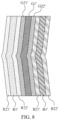
- FIG. 8 is a schematic diagram of a color gamut form of the array substrate according to the second embodiment of the present disclosure.
- FIG. 9 is a schematic diagram of color gamut curves of two common electrodes according to an embodiment of the present disclosure.
- FIG. 10 is a schematic diagram illustrating a top view of an array substrate with a single common electrode
- FIG. 11 is a schematic diagram illustrating a cross-sectional view taken along a line III-III′ regarding the array substrate shown in FIG. 10 ;
- FIG. 12 is a schematic diagram showing a first color gamut comparison between an array substrate with multiple common electrodes and an array substrate with a single common electrode;
- FIG. 13 is a schematic diagram showing a second color gamut comparison between an array substrate with multiple common electrodes and an array substrate with a single common electrode.
- the array substrate includes a substrate U and a plurality of pixel units E.
- the plurality of pixel units E are disposed on the substrate U.
- Each of the pixel units E includes a pixel electrode P, a first common electrode MC, and at least one second common electrode(s) (e.g., SC 1 and/or SC 2 ).
- the number of the at least one second common electrode may be one or more.
- the pixel electrode P is disposed in a first electrode layer L 1 .
- the first common electrode MC is disposed apart from the pixel electrode P.
- An orthographic projection of the first common electrode MC on the substrate U at least partial overlaps an orthographic projection of the pixel electrode P on the substrate U.
- the second common electrode(s) (such as SC 1 and/or SC 2 ) is disposed in a layer in which the first common electrode MC is disposed, e.g., disposed in the second electrode layer L 2 .
- the second common electrode(s) (such as SC 1 and/or SC 2 ) is disposed outside the first common electrode MC in an extension direction of data lines D.
- An orthographic projection of the second common electrode (such as SC 1 and/or SC 2 ) on the substrate U at least partial overlaps an orthographic projection of the pixel electrode P on the substrate U.
- the first common electrode MC and the second common electrode(s) (SC 1 and/or SC 2 ) are insulated from each other.
- the substrate U may be a plate suitable for disposing many material layers of the array substrate, such as glass and the like, which can be used for disposing different material layers in a lamination manner, such as disposing conductive layers, insulation layers, and a passivation layer, and the like.
- an insulation layer can be provided between different conductive layers to insulate different conductive layers (such as electrode layers) from each other.
- exemplary structures related to the characteristics of the embodiments of the present disclosure are illustrated.
- only one of the pixel units E is used as an example for description, but it is not limited to the description here, and the related description can also be applied to a plurality of pixel units.
- the different material layers can be reasonably configured into different components according to actual requirements, such as data lines, scan lines, common lines, common electrodes, thin-film transistors, and pixel electrodes.
- the following description mainly takes two second common electrodes as an example, but the description is not limited here. The relevant descriptions are also applicable to one or more second common electrodes.
- the array substrate may further include a plurality of data lines D and a plurality of scan lines (also called gate lines) A.
- the plurality of data lines D and the plurality of scan lines A are intersected to form a plurality of pixel units E, each of the pixel units E has a pixel electrode P, a first common electrode MC, two second common electrodes SC 1 and SC 2 , and a thin-film transistor T.
- the thin-film transistor T can be used to control an electric field for the pixel unit E, so as to adjust the shape of liquid crystal materials in space and complete functions of the array substrate.
- the array substrate is configured in a form of a lateral-slit FFS mode.
- the first electrode layer L 1 and the second electrode layer L 2 are different conductivity layer.
- the first electrode layer L 1 is configured to have the pixel electrode P.
- the second electrode layer L 2 is configured to have the first common electrode MC and the two second common electrodes SC 1 and SC 2 .
- the first common electrode MC and the two second common electrodes SC 1 and SC 2 are located between the pixel electrode P and the substrate U.
- a circular area in FIG. 1 is an enlarged cross-sectional view taken along a line I-I′ in FIG.
- first common electrode MC and the second common electrode SC 1 are located under the pixel electrode P.
- the first common electrode MC and the two second common electrodes SC 1 and SC 2 are located on a lower side of the pixel electrode P, but are not limited to the description here.
- the first common electrode MC can be configured as a main-common electrode (MAIN COM), the two second common electrodes SC 1 and SC 2 can be regarded as two sub-common electrodes (SUB COM).
- the first common electrode MC is formed into a mirror-symmetrical structure along a virtual plane N perpendicular to the substrate U.
- the first common electrode MC is formed into a mirror-symmetrical trapezoidal structure along the virtual plane N, but is not limited to the description here.
- the two second common electrodes SC 1 and SC 2 can be symmetrically arranged on two sides of the first common electrode MC.
- the two second common electrodes SC 1 and SC 2 can be arranged on two sides of the first common electrode MC in an extension direction of the data lines D.
- the two second common electrodes SC 1 and SC 2 are formed into structures being mutually mirror-symmetrical along the virtual plane N.
- the two second common electrodes SC 1 and SC 2 can be formed into trapezoidal structures being mutually mirror-symmetrical along the virtual plane N, but is not limited to the description here, e.g., the second common electrodes SC 1 and SC 2 can also be configured to form into a structure shaped in other shapes. Therefore, adopting a structure of one main-common electrode and two sub-common electrodes can reduce the coupling effect of different common voltages on adjacent pixel electrodes in the extension direction of the scan lines, so that signal crosstalk can be reduced.
- the pixel electrode P forms a mirror-symmetrical structure along the virtual plane N.
- the pixel electrode P has a plurality of first branch electrodes Y arranged in intervals, a slit is formed between adjacent two of the first branch electrodes Y.
- An angle ⁇ 1 between the virtual plane N and an extension direction F 11 of a part of the first branch electrodes Y located on one side of the virtual plane N is identical to another angle ⁇ 1 between the virtual plane N and an extension direction F 12 of a part of the first branch electrodes Y located on the other side of the virtual plane N.
- the extension direction of the first branch electrode Y refers to a direction extending along an edge on one side of the first branch electrode Y or a direction extending along a virtual central line between edges on two opposite side of the first branch electrode Y
- the angle refers to an angle between the virtual plane N and a direction of the first branch electrodes Y extending from the virtual plane N to a position at the same distance on one of two sides from the virtual plane N.
- the characteristics of the plurality of first branch electrodes e.g., an electrode width or a slit width can be fine-tuned according to the requirements).
- the plurality of first branch electrodes Y are arranged in a mirror symmetry manner on two opposite sides of the virtual plane N.
- the shape of the slits (such as width and extension direction) between the adjacent branch electrodes Y can correspond to a layout of the first common electrode MC and the two second common electrodes SC 1 and SC 2 .
- An extension direction of the electrode gap and an extension direction of the slits between the adjacent branch electrodes Y can be the same.
- a width of one slit closest to the electrode gap is greater than a width of other slits, and the width of one slit closest to the electrode gap is greater than a width of the electrode gap, but are not limited to the description here.
- the pixel electrode P may further include two first trunk electrodes Z, wherein one of the two first trunk electrodes Z is connected to one end of each of the plurality of first branch electrodes Y, and the other of the two first trunk electrodes Z is connected to the other end of each of the plurality of first branch electrodes Y.
- the two first trunk electrodes Z are arranged in parallel to each other.
- the pixel electrode P may further include an extension electrode X.
- the extension electrode X is connected between one of the two first trunk electrodes Z and a control element (such as a thin-film transistor T), so that the control element can transmit a signal to control the electric field of the pixel electrode P, so as to regulate display effects of different display domains.
- the array substrate may further include a first common electrode line Ma and a second common electrode line Sa that can be used to transmit different signals.
- the first common electrode line Ma is connected to the first common electrode MC.
- the second common electrode line Sa is connected to the second common electrodes SC 1 and SC 2 .
- the first common electrode line Ma and the second common electrode line Sa are configured to provide different signals.
- the plurality of first common electrodes MC are connected to the first common electrode line Ma
- the second common electrodes SC 1 and SC 2 are connected to the second common electrode line Sa.
- the first common electrode line Ma and the second common electrode line Sa can be configured to provide different signals, e.g., different signals from a number of gold bumps GB within a non-overlapping region between the array substrate K 1 and the color filter substrate K 2 .
- the array substrate includes a substrate U′ and a plurality of pixel units E′.
- the plurality of pixel units E′ are disposed on the substrate U′.
- Each of the pixel units E′ includes a pixel electrode P′, a first common electrode MC′, and at least a second common electrode(s) (e.g., SC 1 ′ and/or SC 2 ′).
- the pixel electrode P′ is, for example, disposed in the first electrode layer L 1 ′.
- One first common electrode MC′ is disposed apart from the pixel electrode P′.
- An orthographic projection of the first common electrode MC′ on the substrate U′ at least partially overlaps an orthographic projection of the pixel electrode P′ on the substrate U′.
- One second common electrode SC 1 ′ or SC 2 ′ is disposed in a layer in which the first common electrode MC′ is disposed, e.g., disposed in the second electrode layer L 2 ′.
- the second common electrode SC 1 ′ or SC 2 ′ is disposed outside the first common electrode MC′ in an extension direction of scan lines A.
- An orthographic projection of the second common electrode SC 1 ′ or SC 2 ′ on the substrate U′ at least partially overlaps an orthographic projection of the second common electrode SC 1 ′ or SC 2 ′.
- the substrate U′ may be a plate suitable for disposing many material layers of the array substrate, such as glass and the like, which can be used for disposing different material layers in a lamination manner, such as disposing conductive layers, insulation layers, and a passivation layer, and the like.
- an insulation layer can be provided between different conductive layers to insulate different conductive layers (such as electrode layers) from each other.
- pixel units E′ is used as an example for description, but it is not limited to the description here, and the related description can also be applied to a plurality of pixel units.
- the array substrate may further include a plurality of data lines D and a plurality of scan lines (also called gate lines) A.
- the plurality of data lines D and the plurality of scan lines A are intersected to form a plurality of pixel units E′, each of the pixel units E′ has a pixel electrode P′, a first common electrode MC′, two second common electrodes SC 1 ′ and SC 2 ′, and a thin-film transistor.
- the thin-film transistor can be used to control an electric field for the pixel unit, so as to adjust the shape of liquid crystal materials in space and complete functions of the array substrate.
- the array substrate is configured in a form of a vertical-slit FFS mode.
- the first electrode layer L 1 ′ and the second electrode layer L 2 ′ are of different conductivity layer.
- the first electrode layer L 1 ′ is configured to have the pixel electrode P′.
- the second electrode layer L 2 ′ is configured to have the first common electrode MC′ and the second common electrode(s) SC 1 ′ and/or SC 2 ′.
- the pixel electrode P′ is disposed between the substrate U′ and the first and second common electrodes MC′ and SC 1 ′ and/or SC 2 ′.
- each of the first common electrode MC′ and the second common electrode(s) SC 1 ′ and/or SC 2 ′ forms into a mirror-symmetrical structure along a virtual plane N′ perpendicular to the substrate.
- a circular area in FIG. 3 is an enlarged cross-sectional view taken along a line II-II′ in FIG. 3 and shows that the first common electrode MC′ and the second common electrodes SC 1 ′ and SC 2 ′ are located above the pixel electrode P′.
- the first common electrode MC′ and the two second common electrodes SC 1 ′ and SC 2 ′ are located on an upper side of the pixel electrode P′, but are not limited to the description here.
- the first common electrode MC′ can be configured as a main-common electrode (MAIN COM)
- the two second common electrodes SC 1 ′ and SC 2 ′ can be regarded as two sub-common electrodes (SUB COM).
- the two second common electrodes SC 1 ′ and SC 2 ′ are arranged on two sides of the first common electrode MC′ in an extension direction of the scan line A.
- the first common electrode MC′ and the two second common electrodes SC 1 ′ and SC 2 ′ are formed into mirror-symmetrical structures along a virtual plane N′ (e.g., located at a common line) perpendicular to the substrate U′.
- each of the first common electrode MC′ and the two second common electrodes SC 1 ′ and SC 2 ′ has a plurality of second branch electrodes arranged in intervals.
- the first common electrode MC′ has a plurality of second branch electrodes Y 1 ′ arranged at intervals
- each of the two second common electrodes SC 1 ′ and SC 2 ′ has a plurality of second branch electrodes Y 2 ′ arranged at intervals
- a slit is formed between adjacent two of the second branch electrodes (e.g., Y 1 ′ and Y 2 ′).
- an angle ⁇ 2 between the virtual plane N′ and an extension direction F 21 of a part of the second branch electrodes Y 1 ′ located on one side of the virtual plane N′ is identical to another angle ⁇ 2 between the virtual plane N′ and an extension direction F 22 of a part of the second branch electrodes Y 1 ′ located on the other side of the virtual plane N′.
- the extension direction of the second branch electrode Y 1 ′ refers to a direction extending along an edge on one side of the second branch electrode Y 1 ′ or a direction extending along a virtual central line between edges on two opposite side of the second branch electrode Y 1 ′.
- the angle refers to an angle between the virtual plane N′ and a direction of the second branch electrodes Y 1 ′ extending from the virtual plane N′ to a position at the same distance on one of two sides from the virtual plane N′.
- the related descriptions also apply to the two second common electrodes SC 1 ′ and SC 2 ′.
- the plurality of second branch electrodes (such as Y 1 ′ and Y 2 ′) are arranged in a mirror symmetry manner on two opposite sides of the virtual plane N′.
- the characteristics (such as a width or an extension direction, etc.) of the first common electrode MC′ and the second branch electrodes (such as Y 1 ′ and Y 2 ′) of the two second common electrodes SC 1 ′ and SC 2 ′ can be fine-tuned to form a specific layout according to requirements.
- a plurality of slits formed in the first common electrode MC′ are evenly distributed, and a single slit formed in each of the second common electrodes SC 1 ′ and SC 2 ′ is close to the first common electrode MC′, but are not limited to the description here.
- the first common electrode MC′ further includes two second trunk electrodes Z 1 ′
- the two second common electrodes SC 1 ′ and SC 2 ′ further include two second trunk electrodes Z 2 ′, wherein one of the two second trunk electrodes Z 1 ′ of the first common electrode MC′ is connected to one end of each of the plurality of second branch electrodes Y 1 ′ of the first common electrode MC′, the other of the two second trunk electrodes Z 1 ′ of the first common electrode MC′ is connected to the other end of each of the second branch electrodes Y 1 ′ of the first common electrode MC′, one of the two second trunk electrodes Z 2 ′ of the second common electrode(s) (SC 1 ′ and/or SC 2 ′) is connected to one end of each of the plurality of second branch electrodes Y 2 ′ of the second common electrode(s) (SC 1 ′ and/or SC 2 ′), and the other of the two second trunk electrodes Z 2 ′ of the second common electrode(s) (SC 1 ′ and//or
- the structure of the two sub-common electrodes can reduce the coupling effect of the signals on the two sides of the data lines due to different common voltages, so that signal crosstalk can be reduced.
- the pixel electrode P′ is formed into a mirror-symmetric structure along the virtual plane N′ to correspond mirror-symmetric structures of the two second common electrodes (SC 1 ′ and SC 2 ′).
- the array substrate may further include a first common electrode line Ma′ and a second common electrode line Sa′ that can be used to transmit different signals.
- the first common electrode line Ma′ is connected to the first common electrode MC′.
- the second common electrode line Sa′ is connected to the second common electrodes SC 1 ′ and SC 2 ′.
- the first common electrode line Ma′ and the second common electrode line Sa′ are configured to provide different signals.
- the plurality of first common electrodes MC′ are connected to the first common electrode line Ma′
- the second common electrodes SC 1 ′ and SC 2 ′ are connected to the second common electrode line Sa′.
- the first common electrode line Ma′ and the second common electrode line Sa′ can be configured to provide different signals, e.g., different signals from a number of gold bumps GB within a non-overlapping region between the array substrate K 1 and the color filter substrate K 2 .
- the first common electrode and the two second common electrodes can be used to fine-tune color gamut by providing different power supply configurations.
- first common electrode MC and the two second common electrodes SC 1 and SC 2 (as shown in FIGS. 1 and 2 A ) of the first embodiment are used as an example for illustration, and the related descriptions are also applicable to the first common electrode MC′ and the two second common electrodes SC 1 ′ and SC 2 ′ of the second embodiment (as shown in FIGS. 3 and 4 A ).
- the first, second, third, and fourth frames are respectively “+”, “ ⁇ ”, “+”, and “ ⁇ ” inversion potentials
- VMC and VSC respectively represent voltages of the first and second common electrodes (i.e., the main-common electrode and the sub-common electrode). It can be seen from the figure, there is a voltage difference between the voltage VMC of the first common electrode and the voltage VSC of the second common electrode. For example, during potential inversion in different frames, polarities of both the voltage VMC of the first common electrode and the voltage VSC of the second common electrode will change.
- the voltage VMC of the first common electrode and the voltage VSC of the second common electrode is configured in a form of alternating current (A/C), and an absolute value of a voltage amplitude of the voltage VMC of the first common electrode is greater than an absolute value of a voltage amplitude of the voltage VSC of the second common electrode, so that there exists a first voltage difference between the pixel electrode and the first common electrode, and there exists a second voltage difference between the pixel electrode and the second common electrode, wherein an absolute value of the first pressure difference is greater than an absolute value of the second pressure difference.
- Voltage differences always exist regardless of the display state of medium and low grayscales or high grayscales.
- the color gamut can be fine-tuned by providing different power supply configurations, not limited to the description here.
- the first, second, third, and fourth frames are respectively “+”, “ ⁇ ”, “+”, and “ ⁇ ” inversion potentials
- VMC and VSC respectively represent voltages of the first and second common electrodes. It can be seen from the figure, there is a voltage difference between the voltage VMC of the first common electrode and the voltage VSC of the second common electrode. For example, during potential inversion in different frames, polarity of the voltage VMC of the first common electrode will change, and polarity of the voltage VSC of the second common electrode will not change.
- the voltage VMC of the first common electrode is configured in a form of alternating current (A/C)
- the voltage VSC of the second common electrode is configured in a form of direct current (D/C).
- an absolute value of a voltage amplitude of the voltage VMC of the first common electrode is greater than an absolute value of a voltage amplitude of the second common electrode VSC, so that there exists a first voltage difference between the pixel electrode and the first common electrode, there exists a second voltage difference between the pixel electrode and the second common electrode, wherein an absolute value of the first differential pressure is greater than an absolute value of the second differential pressure.
- Voltage differences always exist regardless of the display state of medium and low grayscales or high grayscales.
- the color gamut can be fine-tuned by providing different power supply configurations.
- red (R), green (G), and blue (B) sub-pixels are shown in color gamut forms of the array substrate of the first embodiment.
- a left part shows the red sub-pixel in which color gamut within a display area R 1 corresponding to the first common electrode MC is higher than color gamut within each of display areas R 21 and R 22 corresponding to the two second common electrodes SC 1 and SC 2 .
- a middle part shows the green sub-pixel in which color gamut within a display area G 1 corresponding to the first common electrode MC is higher than color gamut within each of display areas G 21 and G 22 corresponding to the two second common electrodes SC 1 and SC 2 .
- a right part shows the blue sub-pixel in which color gamut within a display area B 1 corresponding to the first common electrode MC is higher than color gamut within each of display areas B 21 and B 22 corresponding to the two second common electrodes SC 1 and SC 2 .
- red (R), green (G), and blue (B) sub-pixels are shown in color gamut forms of the array substrate of the second embodiment.
- a left part shows the red sub-pixel in which color gamut within a display area R 1 ′ corresponding to the first common electrode MC′ is higher than color gamut within each of display areas R 21 ′ and R 22 ′ corresponding to the two second common electrodes SC 1 ′ and SC 2 ′.
- a middle part shows the green sub-pixel in which color gamut within a display area G 1 ′ corresponding to the first common electrode MC′ is higher than color gamut within each of display areas G 21 ′ and G 22 ′ corresponding to the two second common electrodes SC 1 ′ and SC 2 ′.
- a right part shows the blue sub-pixel in which color gamut within a display area B 1 ′ corresponding to the first common electrode MC′ is higher than color gamut within each of display areas B 21 ′ and B 22 ′ corresponding to the two second common electrodes SC 1 ′ and SC 2 ′.
- the description is not limited here, the above description can also be adapted to other sub-pixel configurations, such as an RGBW configuration, to fine-tune the color gamut by providing power supply configurations for different common electrodes.
- the array substrate of the embodiments of the present disclosure has a variety of common electrodes, and only two kinds of common electrodes are used as examples for description, so as to fine-tune the color gamut by providing two power supply configurations, but are not limited to the description here.
- the second electrode layer can be configured to have a first common electrode, two second common electrodes, and two third common electrodes, wherein the first common electrode is located between the two second common electrodes, the two third common electrodes are located on both sides of the first common electrode, and the two second common electrodes are located between the first common electrode and the two third common electrodes.
- the first common electrode is located between the two second common electrodes, and the other groups of common electrodes (such as two third common electrodes, two fourth common electrodes, and the like) are located on both sides of the first common electrode and are sequentially arranged in parallel outside the two second common electrodes, which will not be repeated.
- FIG. 9 shows a schematic diagram of color gamut curves of an array substrate with various common electrodes according to an embodiment of the present disclosure.
- a curve C 1 shows a relationship between transmittance (Transmittance, Tr) and voltage of the first common electrode
- a curve C 2 shows a relationship between transmittance and voltage of the second common electrode, wherein the curve C 1 indicates that the first common electrode covers 82% of the entire color gamut, and the curve C 2 indicates that the second common electrode covers 65% of the entire color gamut.
- an array substrate 9 with a single common electrode includes a single pixel electrode 91 and a single common electrode 92 , wherein a cross-sectional schematic diagram of a line III-III′ is shown in FIG. 11 , and the common electrode 92 is disposed under the pixel electrode 91 .
- a curve C 3 represents a relationship between color gamut and grayscale of the array substrate with a single common electrode provided above
- a curve C 4 represents a relationship between color gamut and grayscale of the array substrate with multiple common electrodes of the above-mentioned embodiments of the present disclosure.
- the array substrate with multiple common electrodes according to the above embodiments of the present disclosure can improve the color gamut of medium and low grayscales in the case of maintaining the transmittance.
- a curve C 5 represents a relationship between color gamut and grayscale of the array substrate with a single common electrode provided above
- a curve C 6 represents a relationship between color gamut and grayscale of the array substrate with multiple common electrodes of the above-mentioned embodiments of the present disclosure.
- the array substrate with multiple common electrodes according to the above embodiments of the present disclosure can slightly reduce the color gamut of grayscale of 255 and improve the color gamut of medium and low grayscales.
- the display device such as a liquid crystal display device.
- the display device includes an opposed substrate, a liquid crystal layer, and an array substrate as mentioned above, wherein the opposed substrate and the array substrate are disposed apart from and opposite to each other, and the liquid crystal layer is disposed between the opposed substrate and the array substrate. Implementations and beneficial effects of the array substrate are described above and will not be repeated here.
- the array substrate and the display device of the above embodiments of the present disclosure are provided in a form of that the first common electrode is disposed apart from the pixel electrode, the orthographic projection of the first common electrode on the substrate at least partially overlaps the orthographic projection of the pixel electrode on the substrate, the at least one second common electrode disposed within the layer in which the first common electrode is disposed, the orthographic projection of the second common electrode on the substrate at least partially overlaps the orthographic projection of the pixel electrode on the substrate, and the first common electrode and the second common electrode are insulated from each other. Therefore, in a case that transmittance can be maintained, color gamut of medium and low grayscales is improved. In addition, in a case that the transmittance is increased, the color gamut of grayscale of 255 is slightly reduced, and the color gamut of the medium and low grayscales is improved.
Landscapes
- Physics & Mathematics (AREA)
- Nonlinear Science (AREA)
- Mathematical Physics (AREA)
- Chemical & Material Sciences (AREA)
- Crystallography & Structural Chemistry (AREA)
- General Physics & Mathematics (AREA)
- Optics & Photonics (AREA)
- Geometry (AREA)
- Engineering & Computer Science (AREA)
- Microelectronics & Electronic Packaging (AREA)
- Liquid Crystal (AREA)
- Devices For Indicating Variable Information By Combining Individual Elements (AREA)
Abstract
Description
Claims (17)
Applications Claiming Priority (3)
| Application Number | Priority Date | Filing Date | Title |
|---|---|---|---|
| CN202210259582.X | 2022-03-16 | ||
| CN202210259582.XA CN114660856B (en) | 2022-03-16 | 2022-03-16 | Array substrate and display device |
| PCT/CN2022/083726 WO2023173483A1 (en) | 2022-03-16 | 2022-03-29 | Array substrate and display apparatus |
Publications (2)
| Publication Number | Publication Date |
|---|---|
| US20240053643A1 US20240053643A1 (en) | 2024-02-15 |
| US12066724B2 true US12066724B2 (en) | 2024-08-20 |
Family
ID=82029424
Family Applications (1)
| Application Number | Title | Priority Date | Filing Date |
|---|---|---|---|
| US17/765,456 Active US12066724B2 (en) | 2022-03-16 | 2022-03-29 | Array substrate and display device |
Country Status (4)
| Country | Link |
|---|---|
| US (1) | US12066724B2 (en) |
| JP (1) | JP7614191B2 (en) |
| CN (1) | CN114660856B (en) |
| WO (1) | WO2023173483A1 (en) |
Families Citing this family (1)
| Publication number | Priority date | Publication date | Assignee | Title |
|---|---|---|---|---|
| CN115877617B (en) * | 2022-12-19 | 2024-10-18 | 惠科股份有限公司 | Array substrate, liquid crystal display panel, driving method and liquid crystal display device |
Citations (13)
| Publication number | Priority date | Publication date | Assignee | Title |
|---|---|---|---|---|
| US20090160748A1 (en) | 2007-12-18 | 2009-06-25 | Yohei Kimura | Liquid crystal display device |
| JP2009198831A (en) | 2008-02-21 | 2009-09-03 | Epson Imaging Devices Corp | Liquid crystal display |
| JP2009223167A (en) | 2008-03-18 | 2009-10-01 | Epson Imaging Devices Corp | Liquid crystal display device |
| JP2013246250A (en) | 2012-05-24 | 2013-12-09 | Mitsubishi Electric Corp | Tft array substrate and liquid crystal panel with the same |
| CN105652530A (en) | 2016-02-19 | 2016-06-08 | 友达光电股份有限公司 | Liquid crystal display panel |
| CN106338864A (en) | 2016-08-25 | 2017-01-18 | 合肥京东方光电科技有限公司 | Array substrate, driving method, liquid crystal display panel and display device |
| CN107331364A (en) | 2017-08-24 | 2017-11-07 | 昆山龙腾光电有限公司 | Liquid crystal display panel and its driving method |
| CN107527924A (en) | 2017-08-18 | 2017-12-29 | 深圳市华星光电技术有限公司 | A kind of array base palte and preparation method thereof, liquid crystal display panel |
| JP2018010229A (en) | 2016-07-15 | 2018-01-18 | 株式会社半導体エネルギー研究所 | Display device, display module, electronic apparatus, and manufacturing method of display device |
| CN108957875A (en) | 2018-09-10 | 2018-12-07 | 惠科股份有限公司 | Pixel structure and liquid crystal display device |
| CN109154749A (en) | 2017-04-01 | 2019-01-04 | 京东方科技集团股份有限公司 | Array substrate, liquid crystal display panel and liquid crystal display device |
| CN109164655A (en) | 2018-09-28 | 2019-01-08 | 合肥鑫晟光电科技有限公司 | Array substrate, display device and its preparation and driving method, base plate preparation method |
| CN111381411A (en) | 2020-04-30 | 2020-07-07 | 厦门天马微电子有限公司 | Array substrate, display panel and display device |
Family Cites Families (6)
| Publication number | Priority date | Publication date | Assignee | Title |
|---|---|---|---|---|
| TWI444730B (en) * | 2006-12-29 | 2014-07-11 | Innolux Corp | Pixel structure, and liquid crystal display panel and liquid crystal display device using the same |
| CN100507694C (en) * | 2007-06-26 | 2009-07-01 | 上海广电光电子有限公司 | Multi-domain vertical alignment mode liquid crystal display device |
| CN105278180B (en) * | 2015-11-05 | 2019-01-04 | 京东方科技集团股份有限公司 | Dot structure and preparation method thereof, array substrate and display panel |
| CN106773378B (en) * | 2017-01-20 | 2019-10-01 | 京东方科技集团股份有限公司 | Array substrate and preparation method thereof, display panel and display device |
| CN107463040B (en) * | 2017-08-28 | 2020-11-10 | 京东方科技集团股份有限公司 | A display substrate, a display panel and a display device |
| CN109239994A (en) * | 2018-10-25 | 2019-01-18 | 京东方科技集团股份有限公司 | array substrate and display device |
-
2022
- 2022-03-16 CN CN202210259582.XA patent/CN114660856B/en active Active
- 2022-03-29 JP JP2022520902A patent/JP7614191B2/en active Active
- 2022-03-29 WO PCT/CN2022/083726 patent/WO2023173483A1/en not_active Ceased
- 2022-03-29 US US17/765,456 patent/US12066724B2/en active Active
Patent Citations (15)
| Publication number | Priority date | Publication date | Assignee | Title |
|---|---|---|---|---|
| US20090160748A1 (en) | 2007-12-18 | 2009-06-25 | Yohei Kimura | Liquid crystal display device |
| JP2009150925A (en) | 2007-12-18 | 2009-07-09 | Toshiba Matsushita Display Technology Co Ltd | Liquid crystal display device |
| JP2009198831A (en) | 2008-02-21 | 2009-09-03 | Epson Imaging Devices Corp | Liquid crystal display |
| JP2009223167A (en) | 2008-03-18 | 2009-10-01 | Epson Imaging Devices Corp | Liquid crystal display device |
| JP2013246250A (en) | 2012-05-24 | 2013-12-09 | Mitsubishi Electric Corp | Tft array substrate and liquid crystal panel with the same |
| CN105652530A (en) | 2016-02-19 | 2016-06-08 | 友达光电股份有限公司 | Liquid crystal display panel |
| JP2018010229A (en) | 2016-07-15 | 2018-01-18 | 株式会社半導体エネルギー研究所 | Display device, display module, electronic apparatus, and manufacturing method of display device |
| CN106338864A (en) | 2016-08-25 | 2017-01-18 | 合肥京东方光电科技有限公司 | Array substrate, driving method, liquid crystal display panel and display device |
| CN109154749A (en) | 2017-04-01 | 2019-01-04 | 京东方科技集团股份有限公司 | Array substrate, liquid crystal display panel and liquid crystal display device |
| CN107527924A (en) | 2017-08-18 | 2017-12-29 | 深圳市华星光电技术有限公司 | A kind of array base palte and preparation method thereof, liquid crystal display panel |
| CN107331364A (en) | 2017-08-24 | 2017-11-07 | 昆山龙腾光电有限公司 | Liquid crystal display panel and its driving method |
| CN108957875A (en) | 2018-09-10 | 2018-12-07 | 惠科股份有限公司 | Pixel structure and liquid crystal display device |
| CN109164655A (en) | 2018-09-28 | 2019-01-08 | 合肥鑫晟光电科技有限公司 | Array substrate, display device and its preparation and driving method, base plate preparation method |
| US20210407354A1 (en) * | 2018-09-28 | 2021-12-30 | Hefei Xinsheng Optoelectronics Technology Co., Ltd. | Array substrate and manufacturing method thereof, display device and driving method thereof and manufacturing method of display substrate |
| CN111381411A (en) | 2020-04-30 | 2020-07-07 | 厦门天马微电子有限公司 | Array substrate, display panel and display device |
Non-Patent Citations (3)
| Title |
|---|
| International Search Report and the Written Opinion Dated Nov. 30, 2022 From the International Searching Authority Re. Application No. PCT/CN2022/083726 and its Translation Into English. (17 Pages). |
| Notice of Reasons for Refusal Dated May 14, 2024 From the Japan Patent Office Re. Application No. 2022-520902 and Its Translation Into English. (10 Pages). |
| Notification of Office Action and Search Report Dated Jun. 12, 2023 From the State Intellectual Property Office of the People's Republic of China Re. Application No. 202210259582.X and its Translation Into English. (20 Pages). |
Also Published As
| Publication number | Publication date |
|---|---|
| JP7614191B2 (en) | 2025-01-15 |
| CN114660856A (en) | 2022-06-24 |
| CN114660856B (en) | 2024-02-20 |
| WO2023173483A1 (en) | 2023-09-21 |
| US20240053643A1 (en) | 2024-02-15 |
| JP2024519559A (en) | 2024-05-17 |
Similar Documents
| Publication | Publication Date | Title |
|---|---|---|
| JP5368590B2 (en) | Liquid crystal display | |
| US20080316413A1 (en) | Display panel | |
| US9019184B2 (en) | Liquid crystal display device including specific subpixel arrangement | |
| US9646553B2 (en) | Display device | |
| CN101359120A (en) | Liquid crystal display device having a plurality of pixel electrodes | |
| JPH08179341A (en) | Liquid crystal display device and driving method thereof | |
| CN108257576B (en) | Array substrate and driving method thereof, and liquid crystal display device and driving method thereof | |
| EP3403139B1 (en) | Array substrate, display panel, and display apparatus | |
| US8878761B2 (en) | Liquid crystal display device and method for driving liquid crystal display device | |
| US12066724B2 (en) | Array substrate and display device | |
| CN109116639B (en) | Liquid crystal display device and driving method thereof | |
| CN106353938A (en) | Display panel | |
| CN109164611B (en) | Array substrate and driving method thereof, and liquid crystal display device and driving method thereof | |
| JP4625645B2 (en) | Thin film diode display panel for liquid crystal display device and liquid crystal display device including the same | |
| CN104423111B (en) | A kind of dot structure and array base palte, liquid crystal display device | |
| US10229935B2 (en) | Curved display device having plurality of subpixel electrodes formed in plurality of columns | |
| JPH06118447A (en) | LCD panel | |
| TWI406038B (en) | Pixels having polarity extension regions for multi-domain vertical alignment liquid crystal displays | |
| US12253774B2 (en) | Display panels and methods of driving display panel | |
| US12044936B1 (en) | Array substrate comprising a first subpixel unit having one of a plurality of first electrodes and a second subpixel unit having two of a plurality of third electrodes and LCD panel | |
| CN114815408B (en) | Display panels and display devices | |
| US11086172B2 (en) | Pixel unit, display panel and display device | |
| US9207486B2 (en) | Liquid crystal display apparatus comprising a light shielding layer overlapping outermost conductive patterns of an electrode | |
| CN108873415B (en) | Liquid crystal display device and driving method | |
| CN114488631A (en) | Array substrate and liquid crystal display panel |
Legal Events
| Date | Code | Title | Description |
|---|---|---|---|
| FEPP | Fee payment procedure |
Free format text: ENTITY STATUS SET TO UNDISCOUNTED (ORIGINAL EVENT CODE: BIG.); ENTITY STATUS OF PATENT OWNER: LARGE ENTITY |
|
| AS | Assignment |
Owner name: TCL CHINA STAR OPTOELECTRONICS TECHNOLOGY CO., LTD., CHINA Free format text: ASSIGNMENT OF ASSIGNORS INTEREST;ASSIGNORS:UM, YOONSUNG;LI, JI;HE, XIAOJIN;AND OTHERS;REEL/FRAME:060049/0200 Effective date: 20220106 |
|
| STPP | Information on status: patent application and granting procedure in general |
Free format text: NON FINAL ACTION MAILED |
|
| STPP | Information on status: patent application and granting procedure in general |
Free format text: RESPONSE TO NON-FINAL OFFICE ACTION ENTERED AND FORWARDED TO EXAMINER |
|
| STPP | Information on status: patent application and granting procedure in general |
Free format text: NOTICE OF ALLOWANCE MAILED -- APPLICATION RECEIVED IN OFFICE OF PUBLICATIONS |
|
| ZAAA | Notice of allowance and fees due |
Free format text: ORIGINAL CODE: NOA |
|
| ZAAB | Notice of allowance mailed |
Free format text: ORIGINAL CODE: MN/=. |
|
| STPP | Information on status: patent application and granting procedure in general |
Free format text: PUBLICATIONS -- ISSUE FEE PAYMENT RECEIVED |
|
| STPP | Information on status: patent application and granting procedure in general |
Free format text: PUBLICATIONS -- ISSUE FEE PAYMENT VERIFIED |
|
| STCF | Information on status: patent grant |
Free format text: PATENTED CASE |