US12052522B2 - Solid-state imaging apparatus and electronic device - Google Patents
Solid-state imaging apparatus and electronic device Download PDFInfo
- Publication number
- US12052522B2 US12052522B2 US17/417,208 US202017417208A US12052522B2 US 12052522 B2 US12052522 B2 US 12052522B2 US 202017417208 A US202017417208 A US 202017417208A US 12052522 B2 US12052522 B2 US 12052522B2
- Authority
- US
- United States
- Prior art keywords
- pixel
- transistor
- floating diffusion
- readout
- reset
- Prior art date
- Legal status (The legal status is an assumption and is not a legal conclusion. Google has not performed a legal analysis and makes no representation as to the accuracy of the status listed.)
- Active, expires
Links
- 238000003384 imaging method Methods 0.000 title description 223
- 238000009792 diffusion process Methods 0.000 claims abstract description 505
- 230000003321 amplification Effects 0.000 claims abstract description 284
- 238000003199 nucleic acid amplification method Methods 0.000 claims abstract description 284
- 238000012546 transfer Methods 0.000 claims abstract description 96
- 230000004048 modification Effects 0.000 description 114
- 238000012986 modification Methods 0.000 description 114
- 238000006243 chemical reaction Methods 0.000 description 47
- 238000010586 diagram Methods 0.000 description 35
- 238000005516 engineering process Methods 0.000 description 33
- 239000000758 substrate Substances 0.000 description 32
- 238000012545 processing Methods 0.000 description 26
- 230000002093 peripheral effect Effects 0.000 description 15
- 239000003990 capacitor Substances 0.000 description 13
- 230000003071 parasitic effect Effects 0.000 description 13
- 230000000875 corresponding effect Effects 0.000 description 10
- 239000011159 matrix material Substances 0.000 description 7
- 230000006870 function Effects 0.000 description 5
- 230000003287 optical effect Effects 0.000 description 5
- 238000005070 sampling Methods 0.000 description 5
- 238000000034 method Methods 0.000 description 4
- NRNCYVBFPDDJNE-UHFFFAOYSA-N pemoline Chemical compound O1C(N)=NC(=O)C1C1=CC=CC=C1 NRNCYVBFPDDJNE-UHFFFAOYSA-N 0.000 description 4
- 230000008569 process Effects 0.000 description 4
- XUIMIQQOPSSXEZ-UHFFFAOYSA-N Silicon Chemical compound [Si] XUIMIQQOPSSXEZ-UHFFFAOYSA-N 0.000 description 2
- 230000035945 sensitivity Effects 0.000 description 2
- 229910052710 silicon Inorganic materials 0.000 description 2
- 239000010703 silicon Substances 0.000 description 2
- 101100243108 Saccharomyces cerevisiae (strain ATCC 204508 / S288c) PDI1 gene Proteins 0.000 description 1
- 230000002730 additional effect Effects 0.000 description 1
- 230000004075 alteration Effects 0.000 description 1
- 230000008901 benefit Effects 0.000 description 1
- 230000002596 correlated effect Effects 0.000 description 1
- 238000013461 design Methods 0.000 description 1
- 230000000694 effects Effects 0.000 description 1
- 230000012447 hatching Effects 0.000 description 1
- 239000002184 metal Substances 0.000 description 1
Images


Classifications
-
- H01L27/14603—
-
- H01L27/14612—
-
- H01L27/14643—
-
- H—ELECTRICITY
- H04—ELECTRIC COMMUNICATION TECHNIQUE
- H04N—PICTORIAL COMMUNICATION, e.g. TELEVISION
- H04N25/00—Circuitry of solid-state image sensors [SSIS]; Control thereof
- H04N25/60—Noise processing, e.g. detecting, correcting, reducing or removing noise
- H04N25/62—Detection or reduction of noise due to excess charges produced by the exposure, e.g. smear, blooming, ghost image, crosstalk or leakage between pixels
- H04N25/627—Detection or reduction of inverted contrast or eclipsing effects
-
- H—ELECTRICITY
- H04—ELECTRIC COMMUNICATION TECHNIQUE
- H04N—PICTORIAL COMMUNICATION, e.g. TELEVISION
- H04N25/00—Circuitry of solid-state image sensors [SSIS]; Control thereof
- H04N25/70—SSIS architectures; Circuits associated therewith
- H04N25/709—Circuitry for control of the power supply
-
- H—ELECTRICITY
- H04—ELECTRIC COMMUNICATION TECHNIQUE
- H04N—PICTORIAL COMMUNICATION, e.g. TELEVISION
- H04N25/00—Circuitry of solid-state image sensors [SSIS]; Control thereof
- H04N25/70—SSIS architectures; Circuits associated therewith
- H04N25/71—Charge-coupled device [CCD] sensors; Charge-transfer registers specially adapted for CCD sensors
- H04N25/75—Circuitry for providing, modifying or processing image signals from the pixel array
-
- H—ELECTRICITY
- H10—SEMICONDUCTOR DEVICES; ELECTRIC SOLID-STATE DEVICES NOT OTHERWISE PROVIDED FOR
- H10F—INORGANIC SEMICONDUCTOR DEVICES SENSITIVE TO INFRARED RADIATION, LIGHT, ELECTROMAGNETIC RADIATION OF SHORTER WAVELENGTH OR CORPUSCULAR RADIATION
- H10F39/00—Integrated devices, or assemblies of multiple devices, comprising at least one element covered by group H10F30/00, e.g. radiation detectors comprising photodiode arrays
- H10F39/10—Integrated devices
- H10F39/12—Image sensors
- H10F39/18—Complementary metal-oxide-semiconductor [CMOS] image sensors; Photodiode array image sensors
-
- H—ELECTRICITY
- H10—SEMICONDUCTOR DEVICES; ELECTRIC SOLID-STATE DEVICES NOT OTHERWISE PROVIDED FOR
- H10F—INORGANIC SEMICONDUCTOR DEVICES SENSITIVE TO INFRARED RADIATION, LIGHT, ELECTROMAGNETIC RADIATION OF SHORTER WAVELENGTH OR CORPUSCULAR RADIATION
- H10F39/00—Integrated devices, or assemblies of multiple devices, comprising at least one element covered by group H10F30/00, e.g. radiation detectors comprising photodiode arrays
- H10F39/80—Constructional details of image sensors
- H10F39/802—Geometry or disposition of elements in pixels, e.g. address-lines or gate electrodes
-
- H—ELECTRICITY
- H10—SEMICONDUCTOR DEVICES; ELECTRIC SOLID-STATE DEVICES NOT OTHERWISE PROVIDED FOR
- H10F—INORGANIC SEMICONDUCTOR DEVICES SENSITIVE TO INFRARED RADIATION, LIGHT, ELECTROMAGNETIC RADIATION OF SHORTER WAVELENGTH OR CORPUSCULAR RADIATION
- H10F39/00—Integrated devices, or assemblies of multiple devices, comprising at least one element covered by group H10F30/00, e.g. radiation detectors comprising photodiode arrays
- H10F39/80—Constructional details of image sensors
- H10F39/803—Pixels having integrated switching, control, storage or amplification elements
- H10F39/8037—Pixels having integrated switching, control, storage or amplification elements the integrated elements comprising a transistor
-
- H—ELECTRICITY
- H10—SEMICONDUCTOR DEVICES; ELECTRIC SOLID-STATE DEVICES NOT OTHERWISE PROVIDED FOR
- H10F—INORGANIC SEMICONDUCTOR DEVICES SENSITIVE TO INFRARED RADIATION, LIGHT, ELECTROMAGNETIC RADIATION OF SHORTER WAVELENGTH OR CORPUSCULAR RADIATION
- H10F39/00—Integrated devices, or assemblies of multiple devices, comprising at least one element covered by group H10F30/00, e.g. radiation detectors comprising photodiode arrays
- H10F39/80—Constructional details of image sensors
- H10F39/813—Electronic components shared by multiple pixels, e.g. one amplifier shared by two pixels
Definitions
- the technology according to the present disclosure (the present technology) relates to a solid-state imaging apparatus and an electronic device.
- a source follower CMOS image sensor that performs readout with a source follower circuit using an amplification transistor.
- a differential amplification CIS capable of increased gain and significantly higher conversion efficiency compared to a source follower CIS (see PTLs 1 to 3 and NPL 1).
- a differential amplifier is formed by a readout pixel from which a pixel signal is read out and a reference pixel from which a pixel signal is not read out, and a pixel signal differentially amplified by the differential amplifier is read out.
- a light detecting device including one or more switch transistors, a first pixel including a first photoelectric converter, a first floating diffusion region coupled to the first photoelectric converter through a first transfer transistor, and a first amplification transistor coupled to the first floating diffusion region, a second pixel in a column in which the first pixel is disposed, the second pixel including a second photoelectric converter, a second floating diffusion region coupled to the second photoelectric converter through a second transfer transistor, and a second amplification transistor coupled to the second floating diffusion region, and a third pixel in the column, the third pixel including a third photoelectric converter, a third floating diffusion region coupled to the third photoelectric converter through a third transfer transistor, and a third amplification transistor coupled to the third floating diffusion region, wherein a pixel signal is differentially amplified by the first amplification transistor and the third amplification transistor, and wherein the first floating diffusion region and the second floating diffusion region are selectively connected to each other via one of the one or
- a light detecting device above that further includes a plurality of reset transistors, the plurality of reset transistors including a first reset transistor configured to reset the first floating diffusion region, a second reset transistor configured to reset the second floating diffusion region, and a third reset transistor configured to reset the third floating diffusion region.
- a light detecting device above, wherein a source of the first reset transistor or a drain of the first reset transistor is coupled to a power supply voltage, and a source of the third reset transistor or a drain of the third reset transistor is coupled to a first voltage line that provides a first voltage different from the power supply voltage.
- a light detecting device above that further includes a fourth pixel in the column, the fourth pixel including a fourth photoelectric converter, a fourth floating diffusion region coupled to the fourth photoelectric converter through a fourth transfer transistor, and a fourth amplification transistor coupled to the fourth floating diffusion region, wherein the third floating diffusion region and the fourth floating diffusion region are selectively connected to each other via a second one of the one or more switch transistors.
- a light detecting device above that further includes a current supply (VCOM) line that is disposed adjacent to the column, and an output signal (VSL) line that is disposed adjacent to the column.
- VCOM current supply
- VSL output signal
- a light detecting device above, wherein the current supply line is disposed between the first amplification transistor and a fourth amplification transistor of a fourth pixel, the fourth pixel disposed in an adjacent column to the column.
- a light detecting device above, wherein the first amplification transistor is coupled to the current supply line, the second amplification transistor is coupled to the current supply line, and the third amplification transistor is coupled to the current supply line.
- a light detecting device above, wherein the first amplification transistor is coupled to the output signal line, and the second amplification transistor is coupled to the output signal line.
- a light detecting device above that further includes a second output signal (VSLR) line that is disposed adjacent to the column, the second output signal line being different than the output signal line, wherein the third amplification transistor is coupled to the second output signal line.
- VSLR second output signal
- the first pixel includes a first switch transistor from the one or more switch transistors, the first switch transistor being the one of the one or more switch transistors that is configured to electrically connect the first floating diffusion region to the second floating diffusion region
- the second pixel includes a second switch transistor from the one or more switch transistors, the second switch transistor configured to electrically connect the second floating diffusion region to a fourth floating diffusion region
- the third pixel includes a third switch transistor from the one or more switch transistors, the third switch transistor configured to electrically connect the third floating diffusion region to a fifth floating diffusion region.
- a light detecting device above that further includes a pixel array including the first pixel, the second pixel, and the third pixel, wherein the third pixel is a reference pixel that is positioned at an edge of the pixel array.
- an electronic apparatus including a light detecting device that includes one or more switch transistors, a first pixel including a first photoelectric converter, a first floating diffusion region coupled to the first photoelectric converter through a first transfer transistor, and a first amplification transistor coupled to the first floating diffusion region, a second pixel in a column in which the first pixel is disposed, the second pixel including a second photoelectric converter, a second floating diffusion region coupled to the second photoelectric converter through a second transfer transistor, and a second amplification transistor coupled to the second floating diffusion region, and a third pixel in the column, the third pixel including a third photoelectric converter, a third floating diffusion region coupled to the third photoelectric converter through a third transfer transistor, and a third amplification transistor coupled to the third floating diffusion region, wherein a pixel signal is differentially amplified by the first amplification transistor and the third amplification transistor, and wherein the first floating diffusion region and the second floating diffusion region are selectively connected to each other via
- the light detecting device further includes a plurality of reset transistors, wherein the plurality of reset transistors includes a first reset transistor configured to reset the first floating diffusion region, a second reset transistor configured to reset the second floating diffusion region, and a third reset transistor configured to reset the third floating diffusion region.
- an electronic apparatus wherein a source of the first reset transistor or a drain of the first reset transistor is coupled to a power supply voltage, and
- a source of the third reset transistor or a drain of the third reset transistor is coupled to a first voltage line that provides a first voltage different from the power supply voltage.
- the light detecting device further includes a fourth pixel in the column, the fourth pixel including a fourth photoelectric converter, a fourth floating diffusion region coupled to the fourth photoelectric converter through a fourth transfer transistor, and a fourth amplification transistor coupled to the fourth floating diffusion region, wherein the third floating diffusion region and the fourth floating diffusion region are selectively connected to each other via a second one of the one or more switch transistors.
- the light detecting device further includes a current supply (VCOM) line that is disposed adjacent to the column, and an output signal (VSL) line that is disposed adjacent to the column.
- VCOM current supply
- VSL output signal
- an electronic apparatus wherein the first amplification transistor is coupled to the current supply line, the second amplification transistor is coupled to the current supply line, and the third amplification transistor is coupled to the current supply line.
- an electronic apparatus wherein the first amplification transistor is coupled to the output signal line, and the second amplification transistor is coupled to the output signal line.
- the first pixel includes a first switch transistor from the one or more switch transistors, the first switch transistor being the one of the one or more switch transistors that is configured to electrically connect the first floating diffusion region to the second floating diffusion region
- the second pixel includes a second switch transistor from the one or more switch transistors, the second switch transistor configured to electrically connect the second floating diffusion region to a fourth floating diffusion region
- the third pixel includes a third switch transistor from the one or more switch transistors, the third switch transistor configured to electrically connect the third floating diffusion region to a fifth floating diffusion region.
- the light detecting device further includes a pixel array including the first pixel, the second pixel, and the third pixel, and wherein the third pixel is a reference pixel that is positioned at an edge of the pixel array.
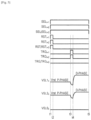
- FIG. 1 is a schematic configuration diagram of a solid-state imaging apparatus according to a first embodiment.
- FIG. 2 is a circuit diagram of a part of the solid-state imaging apparatus according to the first embodiment.
- FIG. 3 is a circuit diagram of a pixel according to the first embodiment.
- FIG. 4 is a circuit diagram of a part of the solid-state imaging apparatus according to the first embodiment.
- FIG. 5 is a timing chart for explaining a readout operation by the solid-state imaging apparatus according to the first embodiment.
- FIG. 6 is a circuit diagram of a part of a solid-state imaging apparatus according to a first modification of the first embodiment.
- FIG. 7 is a circuit diagram of a part of a solid-state imaging apparatus according to a second modification of the first embodiment.
- FIG. 8 is a circuit diagram of a part of a solid-state imaging apparatus according to a third modification of the first embodiment.
- FIG. 9 is a circuit diagram of a part of a solid-state imaging apparatus according to a fourth modification of the first embodiment.
- FIG. 10 is a circuit diagram of a part of the solid-state imaging apparatus according to the fourth modification of the first embodiment.
- FIG. 11 is a timing chart for explaining a readout operation by the solid-state imaging apparatus according to the fourth modification of the first embodiment.
- FIG. 12 is a circuit diagram of a part of a solid-state imaging apparatus according to a fifth modification of the first embodiment.
- FIG. 13 is a timing chart for explaining a readout operation by the solid-state imaging apparatus according to the fifth modification of the first embodiment.
- FIG. 14 is a circuit diagram in a differential amplification readout state of a part of a solid-state imaging apparatus according to a second embodiment.
- FIG. 15 is a circuit diagram in a source follower readout state of a part of the solid-state imaging apparatus according to the second embodiment.
- FIG. 16 is a circuit diagram in a differential amplification readout state of a part of the solid-state imaging apparatus according to the second embodiment.
- FIG. 17 is a timing chart for explaining a differential amplification readout operation by the solid-state imaging apparatus according to the second embodiment.
- FIG. 18 is a circuit diagram in a source follower readout state of the solid-state imaging apparatus according to the second embodiment.
- FIG. 19 is a timing chart for explaining a source follower readout operation by the solid-state imaging apparatus according to the second embodiment.
- FIG. 20 is a circuit diagram in a differential amplification readout state of a part of a solid-state imaging apparatus according to a modification of the second embodiment.
- FIG. 21 is a circuit diagram in a differential amplification readout state of a part of the solid-state imaging apparatus according to the modification of the second embodiment.
- FIG. 22 is a timing chart for explaining a differential amplification readout operation by the solid-state imaging apparatus according to the modification of the second embodiment.
- FIG. 23 is a circuit diagram in a source follower readout state of the solid-state imaging apparatus according to the modification of the second embodiment.
- FIG. 24 is a timing chart for explaining a source follower readout operation by the solid-state imaging apparatus according to the modification of the second embodiment.
- FIG. 25 is a circuit diagram of a part of a solid-state imaging apparatus according to a third embodiment.
- FIG. 26 is a schematic plan view of a part of the solid-state imaging apparatus according to the third embodiment.
- FIG. 27 is a schematic plan view of a part of a solid-state imaging apparatus according to a first modification of the third embodiment.
- FIG. 28 is a circuit diagram of a part of a solid-state imaging apparatus according to a second modification of the third embodiment.
- FIG. 29 is a schematic plan view of a part of a solid-state imaging apparatus according to the second modification of the third embodiment.
- FIG. 30 A is a schematic plan view of a part of a solid-state imaging apparatus according to a third modification of the third embodiment.
- FIG. 30 B is a schematic plan view of another part of a solid-state imaging apparatus according to the third modification of the third embodiment.
- FIG. 31 is a schematic plan view of a part of a solid-state imaging apparatus according to a fourth modification of the third embodiment.
- FIG. 32 is a circuit diagram of a part of a solid-state imaging apparatus according to the fourth embodiment.
- FIG. 33 is a timing chart for explaining a readout operation by the solid-state imaging apparatus according to the fourth embodiment.
- FIG. 34 is a circuit diagram of a part of a solid-state imaging apparatus according to a fifth embodiment.
- FIG. 35 is a circuit diagram of a part of a solid-state imaging apparatus according to a first modification of the fifth embodiment.
- FIG. 36 A is a circuit diagram illustrating the parasitic capacitance of amplification transistors connected in parallel.
- FIG. 36 B is a circuit diagram illustrating the parasitic capacitance of an amplification transistor.
- FIG. 37 is a circuit diagram of a part of a solid-state imaging apparatus according to a second modification of the fifth embodiment.
- FIG. 38 is a circuit diagram of a part of a solid-state imaging apparatus according to a third modification of the fifth embodiment.
- FIG. 39 is a circuit diagram of a part of a solid-state imaging apparatus according to a fourth modification of the fifth embodiment.
- FIG. 40 is a circuit diagram of a part of a solid-state imaging apparatus according to a fifth modification of the fifth embodiment.
- FIG. 41 is a circuit diagram of a part of a solid-state imaging apparatus according to a sixth modification of the fifth embodiment.
- FIG. 42 is a schematic cross-sectional view illustrating an example of applying a solid-state imaging apparatus according to a sixth embodiment to a front-illuminated CIS.
- FIG. 43 is a schematic cross-sectional view illustrating an example of applying the solid-state imaging apparatus according to the sixth embodiment to a back-illuminated CIS.
- FIG. 44 is a schematic diagram illustrating an example of applying the solid-state imaging apparatus according to the sixth embodiment to a back-illuminated CIS.
- FIG. 45 is a schematic diagram illustrating an example of applying the solid-state imaging apparatus according to the sixth embodiment to a back-illuminated CIS.
- FIG. 46 is a schematic diagram illustrating an example of applying the solid-state imaging apparatus according to the sixth embodiment to an electronic device.
- the first embodiment describes a differential amplification solid-state imaging apparatus in which the number of vertical signal lines can be reduced.
- a CIS is illustrated as an example of the solid-state imaging apparatus according to the first embodiment.
- a CIS captures incident light (image light) from a subject, converts the light intensity of the incident light formed into an image on an imaging surface into electrical signals in units of pixels, and outputs the electrical signals as pixel signals.
- the solid-state imaging apparatus As illustrated in FIG. 1 , the solid-state imaging apparatus according to the first embodiment is provided with a pixel array unit 1 and peripheral circuits ( 2 , 3 , 4 , 5 , 6 , and 7 ).
- the configuration illustrated in FIG. 1 may be provided on a single substrate, or the configuration may have a laminate structure in which a plurality of substrates is stuck together.
- the pixel array unit 1 has a plurality of pixels arranged in a two-dimensional layout of rows and columns (a matrix). Each of the plurality of pixels includes a photoelectric conversion unit capable of photoelectrically converting and internally storing a quantity of charge corresponding to the amount of incident light, and outputting the stored charge as a signal.
- the photoelectric conversion unit includes a photodiode, for example.
- pixel driving lines 8 are respectively connected to every pixel row, and vertical signal lines 9 are respectively connected to every pixel column.
- the pixel driving lines 8 are a group of lines that accept signals such as a transfer signal, a select signal, and a reset signal as input.
- the vertical signal lines 9 are a group of lines such as output signal lines, reset input lines, and current supply lines.
- the peripheral circuits ( 2 , 3 , 4 , 5 , 6 , and 7 ) include a vertical driving unit 2 , a column readout circuit unit 3 , a column signal processing unit 4 , a horizontal driving unit 5 , a signal processing unit 6 , and a system control unit 7 .
- the vertical driving unit 2 includes for example a shift register, an address decoder, or the like. The vertical driving unit 2 successively selects the pixel driving lines 8 , supplies pulses for driving pixels to the selected pixel driving line 8 , and drives each of the pixels in units of rows.
- the column readout circuit unit 3 includes a circuit that supplies a constant current, a current mirror circuit, and the like for every pixel column, and forms a differential amplifier together with transistors inside the pixels of the pixel array unit 1 .
- the column readout circuit unit 3 reads out signals from the pixel array unit 1 to the vertical signal lines 9 .
- the column signal processing unit 4 is disposed for every pixel column, for example, and processes the signals output from individual rows of pixels for every pixel column.
- the column signal processing unit 4 performs signal processing such as correlated double sampling (CDS) and analog-digital (AD) conversion.
- CDS is a process that reduces fixed-pattern noise by reading out a signal from a pixel twice and treating the difference between the two readings as the pixel data.
- the signal read out in the first time is a reset level for example, and is referred to as P-phase level.
- the signal read out in the second time is a signal level for example, and is referred to as D-phase level.
- the horizontal driving unit 5 includes for example a shift register, an address decoder, or the like.
- the horizontal driving unit 5 successively outputs horizontal scan pulses to the column signal processing unit 4 , sequentially selects the column signal processing unit 4 , and causes the selected column signal processing unit 4 to output a processed pixel signal.
- the signal processing unit 6 performs signal processing on the pixel signals output from the column signal processing unit 4 , and outputs processed image data.
- the system control unit 7 generates control signals and clock signals that serve as a reference for operations by the vertical driving unit 2 , the column readout circuit unit 3 , the column signal processing unit 4 , the horizontal driving unit 5 , and the like on the basis of a vertical synchronization signal, a horizontal synchronization signal, and a master clock signal, and outputs the generated clock signals and control signals to the vertical driving unit 2 , the column readout circuit unit 3 , the column signal processing unit 4 , the horizontal driving unit 5 , and the like.
- the pixel array unit 1 includes a plurality of pixels X i,k , X i+1,k , X i+2,k , X i+3,k , X i+4,k , X i+5,k , X i,k+1 , X i+1,k+1 , X i+2,k+1 , X i+3,k+1 , X i+4,k+1 , and X i+5,k+1 arranged in a row direction (horizontal direction) and a column direction (vertical direction).
- the row direction is defined as the left-and-right direction of FIG. 2
- the column direction is defined as the top-and-bottom direction of FIG.
- the pixel X i,k illustrated in FIG. 2 includes a photoelectric conversion unit including a photodiode PD that photoelectrically converts incident light, and a plurality of pixel transistors (T 1 , T 2 , T 3 , and T 4 ) that controls the photoelectrically-converted signal charge.
- the plurality of pixel transistors (TI, T 2 , T 3 , and T 4 ) includes a transfer transistor T 1 , a reset transistor T 2 , a select transistor T 3 , and an amplification transistor T 4 , for example.
- the transfer transistor T 1 , the reset transistor T 2 , the select transistor T 3 , and the amplification transistor T 4 are n-channel MOS transistors, for example.
- the anode of the photodiode PD is grounded, while the cathode of the photodiode PD is connected to the source of the transfer transistor T 1 .
- the drain of the transfer transistor T 1 is connected to a floating diffusion (FD).
- a transfer signal TRG i is applied to the gate of the transfer transistor T 1 .
- the transfer transistor T 1 transfers the signal charge generated by the photodiode PD to the floating diffusion FD on the basis of the transfer signal TRG i .
- the floating diffusion FD is connected to the source of the reset transistor T 2 and the gate of the amplification transistor T 4 .
- the floating diffusion FD stores charge transferred by the transfer transistor T 1 .
- the potential of the floating diffusion FD is modulated according to the amount of charge stored in the floating diffusion FD.
- the source of the amplification transistor T 4 is connected to a current supply line VCOM k , while the drain of the amplification transistor T 4 is connected to the source of the select transistor T 3 .
- the amplification transistor T 4 amplifies the potential of the floating diffusion FD, and outputs a current corresponding to the potential of the floating diffusion FD to an output signal line VSL 0 k .
- the drain of the select transistor T 3 is connected to the output signal line VSL 0 k .
- a select signal SEL i is applied to the gate of the select transistor T 3 .
- the select transistor T 3 selects the pixel X i,k as the readout pixel on the basis of the select signal SEL i .
- the drain of the reset transistor T 2 is connected to a reset input line VRD 0 k .
- a reset signal RST i is applied to the gate of the reset transistor T 2 .
- the reset transistor T 2 discharges (resets) the charge stored in the floating diffusion FD on the basis of the reset signal RST i .
- the source and drain of the reset transistor T 2 may be connected in reverse. In this case, the drain of the reset transistor T 2 is connected to the floating diffusion FD while the source of the reset transistor T 2 is connected to the reset input line VRD 0 k .
- the pixels X i,k , X i+1,k , X i+2,k , X i+3,k , X i+4,k , X i+5,k , X i,k+1 , X i+1,k+1 , X i+2,k+1 , X i+3,k+1 , X i+4,k+1 , and X i+5,k+1 illustrated in FIG. 2 likewise have a configuration similar to the pixel X i,k illustrated in FIG. 3 .
- the transfer signal TRG i is applied to the gate of the transfer transistor
- the reset signal RST i is applied to the gate of the reset transistor
- the select signal SEL i is applied to the gate of the select transistor.
- the transfer signal TRG i+1 is applied to the gate of the transfer transistor
- the reset signal RST i+1 is applied to the gate of the reset transistor
- the select signal SEL i+1 is applied to the gate of the select transistor.
- the transfer signal TRG i+2 is applied to the gate of the transfer transistor, the reset signal RST i+2 is applied to the gate of the reset transistor, and the select signal SEL i+2 is applied to the gate of the select transistor.
- the transfer signal TRG i+3 is applied to the gate of the transfer transistor, the reset signal RST i+3 is applied to the gate of the reset transistor, and the select signal SEL i+3 is applied to the gate of the select transistor.
- the transfer signal TRG i+4 is applied to the gate of the transfer transistor, the reset signal RST i+4 is applied to the gate of the reset transistor, and the select signal SEL i+4 is applied to the gate of the select transistor.
- the transfer signal TRG i+5 is applied to the gate of the transfer transistor, the reset signal RST i+5 is applied to the gate of the reset transistor, and the select signal SEL i+5 is applied to the gate of the select transistor.
- a differential amplifier is formed by the pair (differential pair) of a readout pixel that reads out the signal charge and a reference pixel given a reference voltage with no signal charge.
- the readout pixel is successively selected from among the plurality of pixels X i,k , X i+1,k , X i+2,k , X i+3,k , X i+4,k , X i+5,k , X i,k+1 , X i+1,k+1 , X i+2,k+1 , X i+3,k+1 , X i+4,k+1 , and X i+5,k+1 .
- the reference pixel may be successively selected from among the plurality of pixels X i,k , X i+1,k , X i+2,k , X i+3,k , X i+4,k , X i+5,k , X i,k+1 , X i+1,k+1 , X i+2,k+1 , X i+3,k+1 , X i+4,k+1 , and X i+5,k+1 to track the readout pixel, or the reference pixel may be fixed in advance.
- the reference pixel may be fixed in advance.
- Reset input lines VRD 1 k and VRD 2 k are respectively connected to the drain of the reset transistor of the readout pixels X i+1,k and X i+2,k in the kth column.
- Output signal lines VSL 1 k and VSL 2 k are respectively connected to the drain of the select transistor of the readout pixels X i+1,k and X i+2,k .
- a common current supply line VCOM k is connected to the source of the amplification transistor of the readout pixels X i+1,k and X i+2,k .
- a common reset input line VRD 0 k is connected to the drain of the reset transistor of the reference pixels X i,k and X i+3,k in the kth column.
- a common output signal line VSL 0 k is connected to the drain of the select transistor of the reference pixels X i,k and X i+3,k .
- a common current supply line VCOM k is connected to the source of the amplification transistor of the reference pixels X i,k and X i+3,k .
- Reset input lines VRD 1 k+1 and VRD 2 k+1 are respectively connected to the drain of the reset transistor of the readout pixels X i+1,k+1 and X i+2,k+1 in the (k+1)th column.
- Output signal lines VSL 1 k+1 and VSL 2 k+1 are respectively connected to the drain of the select transistor of the readout pixels X i+1,k+1 and X i+2,k+1 .
- a common current supply line VCOM k+1 is connected to the source of the amplification transistor of the readout pixels X i+1,k+1 and X i+2,k+1 .
- a common reset input line VRD 0 k+1 is connected to the drain of the reset transistor of the reference pixels and X i,k+1 and X i+3,k+1 in the (k+1)th column.
- a common output signal line VSL 0 k+1 is connected to the drain of the select transistor of the reference pixels X i,k+1 and X i+3,k+1 .
- a common current supply line VCOM k+1 is connected to the source of the amplification transistor of the reference pixels X i,k+1 and X i+3,k+1 .
- the column readout circuit unit 3 has a configuration corresponding to each of the kth and (k+1)th columns. As the configuration corresponding to the kth column, the column readout circuit unit 3 includes a switch M 0 k disposed between a reset voltage V rst and the reset input lines VRD 0 k , VRD 1 k , and VRD 2 k .
- the switch M 0 k switches the connection destination of the reset voltage V rst to one of the reset input lines VRD 0 k , VRD 1 k , and VRD 2 k .
- the switch M 0 k connects the connection destination of the reset voltage V rst to the reset input line VRD 0 k connected to the drain of the reset transistor of the reference pixels X i,k and X i+3,k .
- the column readout circuit unit 3 includes transistors T 1 k , T 2 k , T 3 k , and T 4 k that form a current mirror circuit.
- the transistors T 1 k , T 2 k , T 3 k , and T 4 k are p-channel MOS transistors, for example.
- the drains of the transistors T 1 k , T 2 k , T 3 k , and T 4 k are connected to a power supply voltage VDD.
- the gates of the transistors T 1 k , T 2 k , T 3 k , and T 4 k are connected to each other and are also connected to the sources of the transistors T 1 k and T 2 k .
- the transistors T 1 k and T 2 k output a signal current 2 I from the source.
- the transistors T 3 k and T 4 k respectively output a reference current I from the source.
- the column readout circuit unit 3 includes a switch M 1 k disposed between the sources of the transistors T 1 k and T 2 k and the output signal lines VSL 0 k , VSL 1 k , and VSL 2 k , a switch M 2 k disposed between the source of the transistor T 3 k and the output signal lines VSL 0 k , VSL 1 k , and VSL 2 k , and a switch M 3 k disposed between the source of the transistor T 4 k and the output signal lines VSL 0 k , VSL 1 k , and VSL 2 k .
- the switch M 1 k is capable of switching the connection destination of the transistors T 1 k and T 2 k to one of the output signal lines VSL 0 k , VSL 1 k , and VSL 2 k , and is connected to the output signal line VSL 0 k .
- the switch M 2 k is capable of switching the connection destination of the transistor T 3 k to one of the output signal lines VSL 0 k , VSL 1 k , and VSL 2 k , and is connected to the output signal line VSL 1 k .
- the switch M 3 k is capable of switching the connection destination of the transistor T 4 k to one of the output signal lines VSL 0 k , VSL 1 k , and VSL 2 k , and is connected to the output signal line VSL 2 k .
- the column readout circuit unit 3 includes a switch S 1 k disposed between the reset input line VRD 0 k and the output signal line VSL 0 k , a switch S 2 k disposed between the reset input line VRD 1 k and the output signal line VSL 1 k , and a switch S 3 k disposed between the reset input line VRD 2 k and the output signal line VSL 2 k .
- the switch S 1 k is turned on.
- the switch S 2 k is turned off, shorting the reset input line VRD 1 k and the output signal line VSL 1 k .
- the switch S 3 k is turned off, shorting the reset input line VRD 2 k and the output signal line VSL 2 k .
- the column readout circuit unit 3 includes a constant current source L 1 k connected to the current supply line VCOM k .
- the constant current source L 1 k is an n-channel MOS transistor, for example.
- the constant current source L 1 k maintains a constant current 4 I from the current supply line VCOM k .
- the current mirror circuit including the amplification transistors of the readout pixels X i+1,k and X i+2,k , the amplification transistors of the reference pixels X i,k and X i+3,k , and the transistors T 1 k , T 2 k , T 3 k , and T 4 k form with the constant current source L 1 k a differential amplifier that amplifies a pair of differential input voltages.
- One of the pair of differential input voltages is input into the amplification transistors of the readout pixels X i+1,k and X i+2,k , while the other of the pair of differential input voltages is input into the amplification transistors of the reference pixels X i,k and X i+3,k .
- the output voltages amplifying the differential input voltages are output to the column readout circuit unit 3 through the output signal lines VSL 1 k and VSL 2 k connected to the drain of the amplification transistors of the readout pixels X i+1,k and X i+2,k .
- the column readout circuit unit 3 includes a switch M 0 k+1 disposed between the reset voltage V rst and the reset input lines VRD 0 k+1 , VRD 1 k+1 , and VRD 2 k+1 .
- the switch M 0 k+1 is capable of switching the connection destination of the reset voltage V rst to one of the reset input lines VRD 0 k+1 , VRD 1 k+1 , and VRD 2 k+1 , and is connected to the reset input line VRD 0 k+1 .
- the column readout circuit unit 3 includes transistors T 1 k+1 , T 2 k+1 , T 3 k+1 , and T 4 k+1 that form a current mirror circuit.
- the transistors T 1 k+1 , T 2 k+1 , T 3 k+1 , and T 4 k+1 are p-channel MOS transistors, for example.
- the drains of the transistors T 1 k+1 , T 2 k+1 , T 3 k+1 , and T 4 k+1 are connected to a power supply voltage VDD.
- the gates of the transistors T 1 k+1 , T 2 k+1 , T 3 k+1 , and T 4 k+1 are connected to each other and are also connected to the sources of the transistors T 1 k+1 and T 2 k+1 .
- the transistors T 1 k+1 and T 2 k+1 output a signal current 2 I from the source.
- the transistors T 3 k+1 and T 4 k+1 respectively output a reference current I from the source.
- the column readout circuit unit 3 includes a switch M 1 k+1 disposed between the sources of the transistors T 1 k+1 and T 2 k+1 and the output signal lines VSL 0 k+1 , VSL 1 k+1 , and VSL 2 k+1 , a switch M 2 k+1 disposed between the source of the transistor T 3 k+1 and the output signal lines VSL 0 k+1 , VSL 1 k+1 , and VSL 2 k+1 , and a switch M 3 k+1 disposed between the source of the transistor T 4 k and the output signal lines VSL 0 k , VSL 1 k , and VSL 2 k .
- the switch M 1 k+1 switches the connection destination of the transistors T 1 k+1 and T 2 k+1 to one of the output signal lines VSL 0 k+1 , VSL 1 k+1 , and VSL 2 k+1 .
- the switch M 2 k+1 switches the connection destination of the transistor T 3 k+1 to one of the output signal lines VSL 0 k+1 , VSL 1 k+1 , and VSL 2 k+1 .
- the switch M 3 k switches the connection destination of the transistor T 4 to one of the output signal lines VSL 0 k+1 , VSL 1 k+1 , and VSL 2 k+1 .
- the column readout circuit unit 3 includes a switch S 1 k+1 disposed between the reset input line VRD 0 k+1 and the output signal line VSL 0 k+1 , a switch S 2 k+1 disposed between the reset input line VRD 1 k+1 and the output signal line VSL 1 k+1 , and a switch S 3 k+1 disposed between the reset input line VRD 2 k+1 and the output signal line VSL 2 k+1 . Furthermore, the column readout circuit unit 3 includes a constant current source L 1 k+1 connected to the current supply line VCOM k+1 .
- the constant current source L 1 k+1 is an n-channel MOS transistor, for example.
- the constant current source L 1 k+1 maintains a constant current 4 I from the current supply line VCOM k+1 .
- the timing chart in FIG. 5 will be referenced to describe a differential amplification readout operation in the case where the pixels X i,k and X i+3,k in the ith and (i+3)th rows of the kth column are selected as reference pixels while the pixels X i+1,k and X i+2,k in the (i+1)th and (i+2)th rows of the kth column are selected as readout pixels, as illustrated in FIG. 4 .
- a high (H) level is applied as the select signals SEL i and SEL i+3 of the reference pixels X i,k and X i+3,k , and while in addition, the select signals SEL i+1 and SEL i+2 of the readout pixels X i+1,k and X i+2,k are set to the H level.
- the reset signals RST i+1 and RST i+2 of the readout pixels X i+1,k and X i+2,k are set to the H level, resetting the readout pixels X i+1,k and X i+2,k .
- the reset signals RST i and RST i+3 of the reference pixels X i,k and X i+3,k are set to the H level, resetting the reference pixels X i,k and X i+3,k .
- the voltage follower function of the differential amplifier causes the output voltages of the output signal lines VSL 1 k and VSL 2 k to go to the reset level V rst . From the time t 2 to t 3 , the reset level V rst is read out from the output signal lines VSL 1 k and VSL 2 k as the P-phase level.
- the transfer signals TRG i+1 and TRG i+2 of the readout pixels X i+1,k and X i+2,k are set to the H level, the reset level V rst of the output signal lines VSL 1 k and VSL 2 k is inverted and amplified, and the D-phase level is read out.
- the column signal processing unit 4 outputs the difference between the P-phase level and the D-phase level as image data.
- the solid-state imaging apparatus by having the reference pixels X i,k and X i+3,k respectively share the reset input line VRD 0 k connected to the drain of the reset transistor, the output signal line VSL 0 k connected to the drain of the select transistor, and the current supply line VCOM k connected to the source of the amplification transistor, the number of vertical signal lines can be reduced compared to a non-shared configuration. For this reason, the pixels can he miniaturized, and it is also possible to reduce the line area when performing multi-row readout.
- the reference pixels X i,k and X i+3,k do not necessarily have to share all of the reset input line VRD 0 k , the output signal line VSL 0 k , and the current supply line VCOM k .
- the number of vertical signal lines can be reduced if the reference pixels X i,k and X i+3,k share at least one of the reset input line VRD 0 k , the output signal line VSL 0 k , and the current supply line VCOM k .
- the configuration of the pixel array unit 1 is different from the solid-state imaging apparatus according to the first embodiment illustrated in FIG. 2 .
- the pixel array unit 1 includes pixels X i,k , X i+1,k , X i+2,k , X i+3,k , X i+4,k , and X i+5,k in the ith to the (i+5)th rows of the kth column, pixels X j,k+1 , X j+1,k+1 , X j+2,k+1 , X j+3,k+1 , X j+4,k+1 , and X j+5,k+1 in the jth to the (j+5)th rows (where j is an integer) of the (k+1)th column, pixels X i,k+2 , X i+1,k+2 , X i+2,k+2 , X i+3,k+2 , X i+4,k+2 , and X i+5,k+2 in the ith to the (i+5)th rows of the (k+2)th column,
- the pixel X i,k in the ith row is selected as the reference pixel, while the pixel X i+1,k+1 in the (i+1)th row is selected as the readout pixel.
- the pixel X j+1,k+1 in the (j+1)th row is selected as the readout pixel, while the pixel X j+2,k+1 in the (j+2)th row is selected as the reference pixel,
- the readout pixels X i+1,k and X j+1,k+1 are adjacent to each other in the same row.
- the drains of the respective reset transistors of the readout pixels X i+1,k and X j+1,k+1 in the kth and (k+1)th columns are connected to the reset input lines VRD 1 k and VRD 2 k , respectively.
- the sources of the respective amplification transistors of the readout pixels X i+1,k and X j+1,k+1 are connected to a common current supply line VCOM k .
- the drains of the respective select transistors of the readout pixels X i+1,k and X j+1,k+1 are connected to the output signal lines VSL 1 k and VSL 2 k , respectively.
- the drains of the respective reset transistors of the reference pixels X i,k and X j+2,k+1 in the kth and (k+1)th columns are connected to a common reset input line VRD 0 k .
- the sources of the respective amplification transistors of the reference pixels X i,k and X j+2,k+1 are connected to a common current supply line VCOM k .
- the drains of the respective select transistors of the reference pixels X i,k and X j+2,k+1 are connected to a common output signal line VSL 0 k .
- the pixel X i,k+2 in the ith row is selected as the reference pixel
- the pixel X i+1,k+2 in the (i+1)th row is selected as the readout pixel.
- the pixel X j+1,k+1 in the (j+1)th row is selected as the readout pixel
- the pixel X j+2,k+3 in the (j+2)th row is selected as the reference pixel.
- the readout pixels X i+1,k+2 and X j+1,k+3 are adjacent to each other in the same row.
- the drains of the respective reset transistors of the readout pixels X i+1,k+2 and X j+1,k+3 in the (k+2)th and (k+3)th columns are connected to the reset input lines VRD 1 k+1 and VRD 2 k+1 , respectively.
- the sources of the respective amplification transistors of the readout pixels X i+1,k+2 and X j+1,k+3 are connected to a common current supply line VCOM k+1 .
- the drains of the respective select transistors of the readout pixels X i+1,k+2 and X j+1,k+3 are connected to the output signal lines VSL 1 k+1 and VSL 2 k+1 , respectively.
- the drains of the respective reset transistors of the reference pixels X i,k+2 and X j+2,k+3 in the (k+2)th and (k+3)th columns are connected to a common reset input line VRD 0 k+1 .
- the sources of the respective amplification transistors of the reference pixels X i,k+2 and X j+2,k+3 are connected to a common current supply line VCOM k+1 .
- the drains of the respective select transistors of the reference pixels X i,k+2 and X j+2,k+3 are connected to a common output signal line VSL 0 k+1 .
- the rest of the configuration of the solid-state imaging apparatus according to the first modification of the first embodiment is similar to the solid-state imaging apparatus according to the first embodiment illustrated in FIG. 2 , and therefore a duplicate description will be omitted.
- the solid-state imaging apparatus by having the reference pixels X i,k and X j+2,k+1 as well as the reference pixels X i,k+2 and X j+2,k+3 in adjacent columns respectively share the reset input lines VRD 0 k and VRD 0 k+1 connected to the drain of the reset transistor, the output signal lines VSL 0 k and VSL 0 k+1 connected to the drain of the select transistor, and the current supply lines VCOM k , VCOM k+1 connected to the source of the amplification transistor, the number of vertical signal lines can be reduced.
- a solid-state imaging apparatus shares a point in common with the solid-state imaging apparatus according to the first embodiment illustrated in FIG. 2 , namely that in the pixel array unit 1 , the readout pixels X i+1,k , X i+2,k , X i+1,k+1 , and X i+2,k+1 are disposed two at a time in each of the kth and (k+1)th columns.
- the solid-state imaging apparatus according to the second modification of the first embodiment differs from the solid-state imaging apparatus according to the first embodiment illustrated in FIG. 2 in that the reference pixels X i+3,k and X i+3,k+1 are disposed one at a time in each of the kth and (k+1)th columns.
- the reference pixels X i+3,k and X i+3,k+1 are disposed in the same (i+3)th row.
- the output signal line VSL 0 k connected to the drain of the select transistor of the reference pixel X i+3,k and the output signal line VSL 0 k+1 connected to the drain of the select transistor of the reference pixel X i+3,k+1 are shorted by a short line 51 through the switches M 1 k and M 1 k+1 in the column readout circuit unit 3 .
- the current supply line VCOM k connected to the source of the amplification transistor of the reference pixel X i+3,k and the current supply line VCOM k+1 connected to the source of the amplification transistor of the reference pixel X i+3,k+1 are shorted by a short line 52 in the column readout circuit unit 3 .
- the rest of the configuration of the solid-state imaging apparatus according to the second modification of the first embodiment is similar to the solid-state imaging apparatus according to the first embodiment illustrated in FIG. 2 , and therefore a duplicate description will be omitted.
- the solid-state imaging apparatus according to the second modification of the first embodiment, as illustrated in FIG. 7 , by disposing the reference pixels X i+3,k and X i+3,k+1 one at a time in each of the kth and (k+1)th columns and using the short line 51 to short the output signal lines VSL 0 k and VSL 0 k+1 connected to the drain of the select transistor of each of the reference pixels X i+3,k and X i+3,k+1 in the same row while also using the short line 52 to short the current supply lines VCOM k and VCOM k+1 connected to the source of the amplification transistor of each of the reference pixels X i+3,k and X i+3,k+1 in the same row, noise can be reduced. Furthermore, the number of readouts of the reference pixels X i+3,k and X i+3,k+1 per column can be reduced, and power consumption can be reduced.
- a solid-state imaging apparatus differs from the solid-state imaging apparatus according to the first embodiment illustrated in FIG. 2 in that in the pixel array unit 1 , the reference pixels X i,k , X i+3,k , X i+6,k , X i,k+1 , X i+3,k+1 , and X i+6,k+1 are selected more than the readout pixels X i+1,k , X i+2,k , X i+1,k+1 , and X i+2,k+1 .
- the three reference pixels X i,k , X i+3,k , and X i+6,k in the ith, (i+3)th, and (i+6)th rows are selected, while the two readout pixels X i+1,k and X i+2,k in the (i+1)th and (i+2)th rows are selected.
- the three reference pixels X i,k+1 , X i+3,k+1 , and X i+6,k+1 in the ith, (i+3)th, and (i+6)th rows are selected, while the two readout pixels X i+1,k+1 and X i+2,k+1 in the (i+1)th and (i+2)th rows are selected.
- the solid-state imaging apparatus by selecting more of the reference pixels X i,k , X i+3,k , X i+6,k , X i,k+1 , X i+3,k+1 , and X i+6,k+1 than the readout pixels X i+1,k , X i+2,k , X i+1,k+1 , and X i+2,k+1 , noise can be reduced further.
- a solid-state imaging apparatus shares a point in common with the solid-state imaging apparatus according to the first embodiment illustrated in FIG. 2 , namely that the reference pixels X i,k and X i+3,k in the same kth column share the output signal line VSL 0 k , the reset input line VRD 0 k , and the current supply line VCOM k , and in addition, the reference pixels X i,k+1 and X i+3,k+1 in the same (k+1)th column share the output signal line VSL 0 k+1 , the reset input line VRD 0 k+1 , and the current supply line VCOM k+1 .
- the solid-state imaging apparatus differs from the solid-state imaging apparatus according to the first embodiment illustrated in FIG. 2 in that the readout pixels X i+1,k and X i+2,k in the kth column share the reset input line VRD 1 k connected to the drain of the reset transistor, and additionally, the readout pixels X i+1,k+1 and X i+2,k+1 in the (k+1)th column share the reset input line VRD 1 k+1 connected to the drain of the reset transistor.
- the column readout circuit unit 3 includes switches M 11 k and M 12 k disposed between the reset input lines VRD 0 k and VRD 1 k and the output signal lines VSL 0 k , VSL 1 k , and VSL 2 k .
- the switches M 11 k and M 12 k switch the connection of one of the reset input lines VRD 0 k and VRD 1 k and to one of the output signal lines VSL 0 k , VSL 1 k , and VSL 2 k .
- the switch M 11 k connects the reset input line VRD 1 k and the output signal line VSL 1 k .
- the switch M 12 k connects the reset input line VRD 1 k and the output signal line VSL 2 k .
- the column readout circuit unit 3 includes switches M 11 k+1 and M 12 k+1 disposed between the reset input lines VRD 0 k+1 and VRD 1 k+1 and the output signal lines VSL 0 k+1 , VSL 1 k+1 , and VSL 2 k+1 .
- the rest of the configuration of the solid-state imaging apparatus according to the third modification of the first embodiment is similar to the solid-state imaging apparatus according to the first embodiment illustrated in FIG. 2 , and therefore a duplicate description will be omitted.
- the timing chart in FIG. 11 will be referenced to describe a differential amplification readout operation in the case where the pixels X i+1,k and X i+2,k in the (i+1)th and (i+2)th rows of the kth column are selected as readout pixels while the pixels X i,k and X i+3,k in the ith and (i+3)th rows are selected as reference pixels, as illustrated in FIG. 10 .
- the switch M 11 k illustrated in FIG. 10 is put in the closed state, shorting the output signal line VSL 1 k and the reset input line VRD 1 k .
- the reset signal RST i+1 of one readout pixel X i+1,k is set to the H level, resetting the readout pixel X i+1,k .
- the reset signals RST i and RST i+3 of the reference pixels X i,k and X i+3,k are set to the H level, resetting the reference pixels X i,k and X i+3,k . Because the output signal line VSL 1 k and the reset input line VRD 1 k are shorted, the output signal line VSL 1 k goes to the reset level and is read out as the P-phase level.
- the switch M 11 k is put in the open state, electrically isolating the output signal line VSL 1 k and the reset input line VRD 1 k .
- the switch M 12 k is put in the closed state, shorting the reset input line VRD 1 k and the output signal line VSL 2 k .
- the reset signal RST i+2 of the other readout pixel X i+2,k is set to the H level, resetting the readout pixel X i+2,k .
- the reset signals RST i and RST i+3 of the reference pixels X i,k and X i+3,k are set to the H level, resetting the reference pixels X i,k and X i+3,k . Because the reset input line VRD 1 k and the output signal line VSL 2 k are shorted, the output signal line VSL 2 k goes to the reset level and is read out as the P-phase level.
- the switch M 12 k is put in the open state, electrically isolating the reset input line VRD 1 k and the output signal line VSL 2 k .
- the transfer signals TRG i+1 and TRG i+2 of the readout pixels X i+1,k and X i+2,k are set to the H level, and the reset level of the output signal lines VSL 1 k and VSL 2 k is inverted and amplified. After that, the D-phase levels of the output signal lines VSL 1 k and VSL 2 k are read out at the same time.
- the readout pixels X i+1,k and X i+2,k in the kth column share the reset input line VRD 1 k connected to the drain of the reset transistor and also having the readout pixels X i+1,k+1 and X i+2,k+1 in the (k+1)th column share the reset input line VRD 1 k+1 connected to the drain of the reset transistor, the number of vertical signal lines can be reduced further.
- a solid-state imaging apparatus differs from the solid-state imaging apparatus according to the fourth modification of the first embodiment illustrated in FIG. 10 in that, in the pixel array unit 1 , one reference pixel X i,k is selected in the kth column.
- the differential amplification readout operation in this case will be described with reference to the timing chart in FIG. 13 .
- the switch M 11 k illustrated in FIG. 10 is put in the closed state, shorting the output signal line VSL 1 k and the reset input line VRD 1 k connected to the readout pixel X i+1,k reset previously.
- the reset signal RST i of the reference pixel X i,k is set to the H level, resetting the reference pixel X i,k .
- the reset signal RST i+1 of one readout pixel X i+1,k is set to the H level, resetting the readout pixel X i+1,k . Because the output signal line VSL 1 k and the reset input line VRD 1 k are shorted, the output signal line VSL 1 k goes to the reset level, and the P-phase level is read out.
- the switch M 11 k is put in the open state, electrically isolating the output signal line VSL 1 k and the reset input line VRD 1 k .
- the switch M 12 k is put in the closed state, shorting the reset input line VRD 1 k and the output signal line VSL 2 k connected to the readout pixel X i+2,k reset subsequently.
- the reset signal RST i of the reference pixel X i,k is set to the H level, resetting the reference pixel X i,k .
- the reset signal RST i+2 of the other readout pixel X i+2,k is set to the H level, resetting the readout pixel X i+2,k . Because the reset input line VRD 1 k and the output signal line VSL 2 k are shorted, the output signal line VSL 2 k goes to the reset level, and the P-phase level is read out.
- the transfer signal TRG i+1 of the readout pixel X i+1,k is set to the H level, the reset level of the output signal line VSL 1 k is inverted and amplified, and the D-phase level is read out.
- the switch M 12 k is put in the open state, electrically isolating the reset input line VRD 1 k and the output signal line VSL 2 k .
- the transfer signal TRG i+2 of the readout pixel X i+2,k is set to the H level, the reset level of the output signal line VSL 2 k goes to the signal level, and the D-phase level is read out.
- the readouts of the P-phase level and the D-phase level of the readout pixels X i+1,k and X i+2,k selected at the same time are performed with shifted a half-phase away from each other, making it possible to read out the signal level (D phase level) of one readout pixel X i+1,k while at the same time to read out the reset level (P-phase level) of the other readout pixel X i+2,k . Consequently, readout can be sped up and the readout time can be shortened.
- a differential amplification CIS capable of increased gain and significantly higher conversion efficiency compared to a source follower CIS of the related art.
- a differential amplification CIS has a narrow operating point and the dynamic range is difficult to expand. For this reason, a configuration that switches between a differential amplification readout and source follower readout with a switch has been investigated.
- a pixel that switches between source follower readout and differential amplification readout needs additional vertical lines inside the pixel.
- the number of vertical lines is increased to five lines in a pixel that switches between source follower readout and differential amplification readout.
- the second embodiment proposes a solid-state imaging apparatus capable of reducing vertical lines inside pixels in a solid-state imaging apparatus capable of switching between differential amplification readout and source follower readout.
- the overall configuration of the solid-state imaging apparatus according to the second embodiment is shared in common with the solid-state imaging apparatus according to the first embodiment illustrated in FIG. 1 .
- the solid-state imaging apparatus according to the second embodiment differs from the solid-state imaging apparatus according to the first embodiment illustrated in FIG. 2 in that the pixel array unit 1 includes a readout pixel region 1 a and a reference pixel region 1 b.
- the readout pixel region 1 a includes pixels X i,k , X i+1,k , X i+2,k , X i+3,k , X i,k+1 , X i+1,k+1 , X i+2,k+1 , and X i+3,k+1 arranged in a two-dimensional matrix.
- the pixels X i,k , X i+1,k , X i+2,k , X i+3,k , X i,k+1 , X i+1,k+1 , X i+2,k+1 , and X i+3,k+1 included in the readout pixel region 1 a are only selectable as readout pixels, and are not selected as reference pixels.
- each of the readout pixels X i,k , X i+1,k , X i+2,k , X i+3,k , X i,k+1 , X i+1,k+1 , X i+2,k+1 , and X i+3,k+1 is similar to the configuration of the pixel X i,k illustrated in FIG. 3 .
- the sources of the respective amplification transistors of the readout pixels X i,k and X i+2,k in the ith and (i+2)th rows of the kth column are connected to a common current supply line VCOM k .
- the drains of the respective select transistors of the readout pixels X i,k and X i+2,k are connected to a common output signal line VSL 0 k .
- the sources of the respective reset transistors of the readout pixels X i,k and X i+2,k are connected to a floating diffusion, and the drains of the respective reset transistors are connected to a common output signal line VSL 0 k .
- the readout pixels X i,k and X i+2,k form a negative feedback loop connecting the floating diffusion and the output signal line VSL 1 k through the reset transistor, and supply the reset voltage.
- the sources of the respective amplification transistors of the readout pixels X i+1,k and X i+3,k in the (i+1)th and (i+3)th rows of the kth column are connected to a common current supply line VCOM k .
- the drains of the respective select transistors of the readout pixels X i+1,k and X i+3,k are connected to a common output signal line VSL 1 k .
- the sources of the respective reset transistors of the readout pixels X i+1,k and X i+3,k are connected to a floating diffusion, and the drains of the respective reset transistors are connected to a common output signal line VSL 1 k .
- the readout pixels X i+1,k and X i+3,k form a negative feedback loop connecting the floating diffusion and the output signal VSL 1 k through the reset transistor, and supply the reset voltage.
- the sources of the respective amplification transistors of the readout pixels X i,k+1 and X i+2,k+1 in the ith and (i+2)th rows of the (k+1)th column are connected to a common current supply line VCOM k+1 .
- the drains of the respective select transistors of the readout pixels X i,k+1 and X i+2,k+1 are connected to a common output signal line VSL 0 k+1 .
- the sources of the respective reset transistors of the readout pixels and X i,k+1 and X i+2,k+1 are connected to a floating diffusion, and the drains of the respective reset transistors are connected to a common output signal line VSL 0 k+1 . That is, the readout pixels X i,k+1 and X i+2,k+1 form a negative feedback loop connecting the floating diffusion and the output signal line VSL 1 k+1 through the reset transistor, and supply the reset voltage.
- the sources of the respective amplification transistors of the readout pixels X i+1,k+1 and X i+3,k+1 in the (i+1)th and (i+3)th rows of the (k+1)th column are connected to a common current supply line VCOM k+1 .
- the drains of the respective select transistors of the readout pixels X i+1,k+1 and X i+3,k+1 are connected to a common output signal line VSL 1 k+1 .
- the sources of the respective reset transistors of the readout pixels X i+1,k+1 and X i+3,k+1 are connected to a floating diffusion, and the drains of the respective reset transistors are connected to a common output signal line VSL 1 k+1 .
- the readout pixels X i+1,k+1 and X i+3,k+1 form a negative feedback loop connecting the floating diffusion and the output signal line VSL 1 k+1 through the reset transistor, and supply the reset voltage.
- the reference pixel region 1 b includes a plurality of pixels X R,k and X R,k+1 fixed to a specific row of the pixel array unit 1 .
- the pixels X R,k and X R,k+1 are arranged in the Rth row, which is the row positioned closest to the column readout circuit unit 3 among the rows of the pixel array unit 1 .
- the pixels X R,k and X R,k+1 are disposed in correspondence with the kth and (k+1)th columns of the readout pixel region 1 a .
- the pixels X R,k and X R,k+1 are fixed as reference pixels, and are not selected as readout pixels.
- the configuration of each of the reference pixels X R,k and X R,k+1 is similar to the configuration of the pixel X i,k illustrated in FIG. 3 .
- the drains of the respective reset transistors of the reference pixels X R,k and X R,k+1 in the kth and (k+1)th columns are connected to a common reset input line VRD.
- the reference pixels X R,k and X R,k+1 share the reset input line VRD.
- the reset input line VRD is supplied with any reset voltage V rst from a reset voltage source.
- the drains of the respective select transistors of the reference pixels X R,k and X R,k+1 in the kth and (k+1)th columns are connected to output signal lines VSLR k and VSLR k+1 .
- the output signal lines VSLR k and VSLR k+1 are shorted by a short line 61 in the column readout circuit unit 3 .
- the sources of the respective amplification transistors of the reference pixels X R,k and X R,k+1 in the kth and (k+1)th columns are connected to current supply lines VCOM k and VCOM k+1 , respectively.
- the current supply lines VCOM k and VCOM k+1 are shorted by a short line 62 in the column readout circuit unit 3 .
- the column readout circuit unit 3 has a corresponding configuration for each of the kth and (k+1)th columns. As the configuration corresponding to the kth column, the column readout circuit unit 3 includes constant current sources L 1 k and L 2 k .
- the constant current sources L 1 k and L 2 k are n-channel MOS transistors or the like.
- the column readout circuit unit 3 includes transistors T 1 k , T 2 k , and T 3 k that form a current mirror circuit.
- a power supply voltage VDD are connected to the drains of the transistors T 1 k , T 2 k , and T 3 k .
- the gates of the transistors T 1 k , T 2 k , and T 3 k are connected to each other and are also connected to the source of the transistor T 1 k .
- the column readout circuit unit 3 includes a plurality of switches (switching units) S 11 k , S 12 k , S 13 k , S 14 k , S 15 k , S 16 k , S 17 k , S 18 k , S 19 k , and S 20 k that switch the operating point of the amplification transistors of the readout pixels X i,k , X i+1,k , X i+2,k and X i+3,k of the kth column between source follower readout and differential amplification readout.
- switches switching units
- the switch S 11 k is disposed between the source of the transistor T 1 k and the output signal line VSLR k .
- the switch S 12 k is disposed between the source of the transistor T 2 k and the output signal line VSL 0 k .
- the switch S 13 k is disposed between the source of the transistor T 3 k and the output signal line VSL 1 k .
- the switch S 14 k is disposed between the power supply voltage VDD and the current supply line VCOM k .
- the switch S 15 k is disposed between the power supply voltage VDD and the output signal line VSL 0 k .
- the switch S 16 k is disposed between the power supply voltage VDD and the output signal line VSL 1 k .
- the switch S 17 k is disposed between the output signal line VSL 0 k and the constant current source L 1 k .
- the switch S 18 k is disposed between the output signal line VSL 1 k and the constant current source L 2 k .
- the switch S 19 k is disposed between the constant current source L 1 k and the current supply line VCOM k .
- the switch S 20 k is disposed between the constant current source L 2 k and the current supply line VCOM k .
- the column readout circuit unit 3 includes constant current sources L 1 k+1 and L 2 k+1 , and transistors T 1 k+1 , T 2 k+1 , and T 3 k+1 .
- the configuration of each of the constant current sources L 1 k+1 and L 2 k+1 and the transistors T 1 k+1 , T 2 k+1 , and T 3 k+1 is similar to the constant current sources L 1 k and L 2 k and the transistors T 1 k , T 2 k , and T 3 k in the configuration of the kth column.
- the column readout circuit unit 3 includes a plurality of switches (switching units) S 11 k+1 , S 12 k+1 , S 13 k+1 , S 14 k+1 , S 15 k+1 , S 16 k+1 , S 17 k+1 , S 18 k+1 , S 19 k+1 , and S 20 k+1 that switch the operating point of the amplification transistors of the readout pixels X i,k+1 , X i+1,k+1 , X i+2,k+1 and X i+3,k+1 of the (k+1)th column between source follower readout and differential amplification readout.
- switches switching units
- each of the plurality of switches S 11 k+1 , S 12 k+1 , S 13 k+1 , S 14 k+1 , S 15 k+1 , S 16 k+1 , S 17 k+1 , S 18 k+1 , S 19 k+1 , and S 20 k+1 is similar to the plurality of switches S 11 k , S 12 k , S 13 k , S 14 k , S 15 k , S 16 k , S 17 k , S 18 k+1 , S 19 k+1 , and S 20 k+1 is similar to the plurality of switches S 11 k , S 12 k , S 13 k , S 14 k , S 15 k , S 16 k , S 17 k , S 18 k , S 19 k , and S 20 k in the configuration of the kth column.
- FIG. 14 illustrates the differential amplification readout state of the solid-state imaging apparatus according to the second embodiment.
- the switches S 11 k , S 12 k , S 13 k , S 19 k , and S 20 k are in the closed state while the switches S 14 k , S 15 k , S 16 k , S 17 k , and S 18 k are in the open state.
- the switches S 11 k+1 , S 12 k+1 , S 13 k+1 , S 19 k+1 , and S 20 k+1 are in the closed state while the switches S 14 k+1 , S 15 k+1 , S 16 k+1 , S 17 k+1 , and S 18 k+1 are in the open state.
- FIG. 15 illustrates the source follower readout state of the solid-state imaging apparatus according to the second embodiment.
- the switches S 11 k , S 12 k , S 13 k , S 19 k , and S 20 k are in the open state while the switches S 14 k , S 17 k , and S 18 k are in the closed state.
- the switches S 15 k and S 16 k are switched between the open state and the closed state during the source follower readout operation, Also, in the configuration of the (k+1)th column of the column readout circuit unit 3 , the switches S 11 k+1 S 12 k+1 , S 13 k+1 , S 19 k+1 , and S 20 k+1 are in the open state while the switches S 14 k+1 , S 17 k+1 , and S 18 k+1 are in the closed state. The switches S 15 k+1 and S 16 k+1 are switched between the open state and the closed state during the source follower readout operation.
- the timing chart in FIG. 17 will be referenced to describe a differential amplification readout operation in the case where the pixels X i,k+1 and X i+1,k+1 in the ith and (i+1)th rows of the kth column are selected as readout pixels while the reference pixel X R,k is fixed, as illustrated in FIG. 16 .
- a select signal SEL R of the reference pixel X R,k is set to the H level, while in addition, the select signals SEL i and SEL i+1 of the readout pixels X i,k X i+1,k are set to the H level.
- a control signal ⁇ VSW of the switches S 15 k and S 16 k is set to the L level, putting the switches S 15 k and S 16 k in the open state.
- the reset signals RST i and RST i+1 of the readout pixels X i,k and X i+1,k are set to the H level, resetting the readout pixels X i,k and X i+1,k .
- a reset signal RST R of the reference pixel X R,k is set to the H level, resetting the reference pixel X R,k .
- the output signal lines VSL 0 k and VSL 1 k go to the reset level V rst according to the voltage follower function of the differential amplifier. From the time t 2 to t 3 , the reset level V rst is read out from the output signal lines VSL 0 k and VSL 1 k as the P-phase level.
- the transfer signals TRG i and TRG i+1 of the readout pixels X i,k and X i+1,k are set to the H level, the reset level V rst of the output signal lines VSL 0 k and VSL 1 k is inverted and amplified, and after that, the D-phase level is read out.
- FIG. 19 will be referenced to describe a source follower readout operation in the case where the pixels X i,k and X i+1,k in the ith and (i+1)th rows of the kth column are readout pixels, as illustrated in FIG. 18 .
- the select signals SEL i and SEL i+1 of the readout pixels X i,k and X i+1,k are set to the H level.
- the select signal SEL R of the reference pixel X R,k is at the L level, and the reference pixel X R,k is not selected.
- the reset signals RST i and RST i+1 of the readout pixels X i,k and X i+1,k are set to the H level, resetting the readout pixels X i,k and X i+1,k .
- the control signal ⁇ VSW of the switches S 15 k and S 16 k is set to the H level to put the switches S 15 k and S 16 k in the closed state, thereby shorting the output signal lines VSL 0 k and VSL 1 k and the power supply potential VDD.
- the P-phase level is read out from the output signal lines VSL 0 k and VSL 1 k .
- the transfer signals TRG i and TRG i+1 of the readout pixels X i,k and X i+1,k are set to the H level, the P-phase level of the output signal lines VSL 0 k and VSL 1 k is inverted and amplified, and the D-phase level is read out.
- the solid-state imaging apparatus it is possible to switch between source follower readout and differential amplification readout with the plurality of switches (switching units) S 11 k , S 12 k , S 13 k , S 14 k , S 15 k , S 16 k , S 17 k , S 18 k , S 19 k , and S 20 k .
- the readout pixels X i,k , X i+1,k , X i+2,k and X i+3,k form a negative feedback loop connecting the drain of the select transistor and the drain of the reset transistor to the output signal lines VSL 0 k and VSL 1 k , the number of reset input lines can be reduced. Consequently, the vertical lines inside the pixels can be reduced, thereby improving sensitivity and also improving the freedom of line placement.
- the line lengths of the output signal lines VSLR k and VSLR k+1 to which the drains of the respective select transistors of the pixels X R,k and X R,k+1 are connected can be shortened.
- a solid-state imaging apparatus shares a point in common with the solid-state imaging apparatus according to the second embodiment illustrated in FIG. 14 , namely a configuration capable of switching between source follower readout and differential amplification readout.
- FIG. 20 illustrates the state of differential amplification readout.
- the configuration of the readout pixels X i,k , X i+1,k , X i+2,k , X i+3,k , X i,k+1 , X i+1,k+1 , X i+2,k+1 , and X i+3,k+1 included in the readout pixel region 1 a and the reference pixels X R,k and X R,k+1 included in the reference pixel region 1 b is different from the solid-state imaging apparatus according to the second embodiment illustrated in FIG. 14 .
- the readout pixel X i,k included in the readout pixel region 1 a includes two photoelectric conversion units including photodiodes PD 1 and PD 2 that photoelectrically convert incident light, and a plurality of pixel transistors (T 1 a , T 1 b , T 2 a , T 2 b , T 3 , and T 4 ) that controls the photoelectrically-converted signal charge.
- the plurality of pixel transistors includes transfer transistors T 1 a and T 1 b , a reset transistor for source follower readout (source follower reset transistor) T 2 a , a reset transistor for differential amplification readout (differential amplification reset transistor) T 2 b , a select transistor T 3 , and an amplification transistor T 4 , for example,
- the respective anodes of the photoelectric conversion units that is, the photodiodes PD 1 and PD 2
- the respective cathodes of the photodiodes PD 1 and PD 2 are connected to the sources of the transfer transistors T 1 a and T 1 b , respectively.
- the drains of the transfer transistors T 1 a and T 1 b are connected to the floating diffusion FD.
- Transfer signals TRG 0 i and TRG 1 i are respectively applied to the gates of the transfer transistors T 1 a and T 1 b.
- the floating diffusion FD is connected to the sources of the source follower reset transistor T 2 a and the differential amplification reset transistor T 2 b , and to the gate of the amplification transistor T 4 .
- the source of the amplification transistor T 4 is connected to a current supply line VCOM k , while the drain of the amplification transistor T 4 is connected to the source of the select transistor T 3 .
- the drain of the select transistor T 3 is connected to the output signal line VSL 0 k .
- a select signal SEL i is applied to the gate of the select transistor T 3 .
- the drain of the source follower reset transistor T 2 a is connected to the current supply line VCOM k .
- the drain of the differential amplification reset transistor T 2 b is connected to the output signal line VSL 0 k .
- Reset signals RSTS i and RSTD i are respectively applied to the gates of the source follower reset transistor T 2 a and the differential amplification reset transistor T 2 b .
- a reset signal RSTS R is applied to the gates of the respective source follower reset transistors of the reference pixels X R,k and X R,k+1 .
- the drains of the respective source follower reset transistors of the reference pixels X R,k and X R,k+1 are connected to the current supply lines VCOM k and VCOM k+1 .
- a reset signal RSTD R is applied to the gates of the respective differential amplification reset transistors of the reference pixels X R,k and X R,k+1 .
- the drains of the respective differential amplification reset transistors of the reference pixels X R,k and X R,k+1 are connected to a common reset input line VRD.
- the timing chart in FIG. 22 will be referenced to describe a differential amplification readout operation in the modification of the second embodiment in the case where the pixels X i,k+1 and X i+1,k+1 in the ith and (i+1)th rows of the kth column are the readout pixels while the reference pixel X R,k is fixed, as illustrated in FIG. 21 .
- a select signal SEL R of the reference pixel X R,k is set to the H level, while in addition, the select signals SEL i and SEL i+1 of the readout pixels X i,k and X i+1,k are set to the H level.
- a control signal ⁇ VSW of the switches S 15 k and S 16 k is set to the L level, putting the switches S 15 k and S 16 k in the open state.
- the reset signals RSTS i and RSTS i+1 of the readout pixels X i,k and X i+1,k as well as the reset signal RSTS R of the reference pixel X R,k are set to the L level.
- the reset signals RSTD i and RSTD i+1 of the readout pixels X i,k and X i+1,k are set to the H level, resetting the readout pixels X i,k and X i+1,k .
- a reset signal RSTD R of the reference pixel X R,k is set to the H level, resetting the reference pixel X R,k .
- the output signal lines VSL 0 k and VSL 1 k go to the reset level V rst according to the voltage follower function of the differential amplifier. From the time t 2 to t 3 , the reset level V rst is read out from the output signal lines VSL 0 k and VSL 1 k as the P-phase level.
- the transfer signals TRG 0 i and TRG 0 i+1 of the readout pixels X i,k and X i+1,k are set to the H level, the reset level V rst of the output signal lines VSL 0 k and VSL 1 k is inverted and amplified, and the D-phase level is read out.
- FIG. 24 will be referenced to describe a source follower readout operation in the modification of the second embodiment in the case where the pixels X i,k+1 and X i+1,k+1 in the ith and (i+1)th rows are the readout pixels, as illustrated in FIG. 23 .
- the select signals SEL i and SEL i+1 of the readout pixels X i,k X i+1,k are set to the H level.
- the select signal SEL R of the reference pixel X R,k is at the L level, and the reference pixel X R,k is not selected.
- the reset signals RSTD i and RSTD +1 of the readout pixels X i,k and X i+1,k are set to the L level.
- the reset signals RSTS i and RSTS i+1 of the readout pixels X i,k X i+1,k are set to the H level, resetting the readout pixels X i,k and X i+1,k .
- the control signal ⁇ VSW of the switches S 15 k and S 16 k is set to the H level to put the switches S 15 k and S 16 k in the closed state, thereby shorting the output signal lines VSL 0 k and VSL 1 k and the power supply potential VDD.
- the P-phase level is read out from the output signal lines VSL 0 k and VSL 1 k .
- the transfer signals TRG i TRG i+1 and of the readout pixels X i,k and X i+1,k are set to the H level, the P-phase level of the output signal lines VSL 0 k and VSL 1 k is inverted and amplified, and the D-phase level is read out.
- each of the readout pixels X i,k , X i+1,k , X i+2,k , X i+3,k , X i,k+1 , X i+1,k+1 , X i+2,k+1 , and X i+3,k+1 as well as the reference pixels X R,k and X R,k+1 include the source follower reset transistor T 2 a and the differential amplification reset transistor T 2 b , compared to the solid-state imaging apparatus according to the second embodiment illustrated in FIG.
- a differential amplification CIS capable of increased gain and significantly higher conversion efficiency compared to a source follower CIS of the related art.
- the source diffusion layer of the amplification transistor and the source diffusion layer of the reset transistor can be shared among the pixels, whereas in a differential amplification CIS, the source diffusion layer of the amplification transistor and the source diffusion layer of the reset transistor is not shared among the pixels. For this reason, a differential amplification CIS has poor layout efficiency compared to a source follower CIS.
- a third embodiment proposes a solid-state imaging apparatus in which the gate length of the amplification transistor can be lengthened and the RTS noise can be improved even at small pixel sizes.
- a pixel array unit 1 includes pixels X i,k , X i+1,k , X i+2,k , X i+3,k , X i+4,k , X i+5,k , X i,k+1 , X i+1,k+1 , X i+2,k+1 , X i+3,k+1 , X i+4,k+1 , and X i+5,k+1 arranged in a matrix.
- the pixels X i+1,k and X i+2,k in the (i+1)th and (i+2)th rows are selected as readout pixels while the pixel X i+3,k in the (i+3)th row is selected as the reference pixel.
- the pixels X i+1,k+1 and X i+2,k+1 in the (i+1)th and (i+2)th rows are selected as readout pixels while the pixel X i+3,k in the (i+3)th row is selected as the reference pixel.
- the sources of the respective amplification transistors of the readout pixels X i+1,k , X i+2,k , X i+1,k+1 , and X i+2,k+1 as well as the reference pixels X i+3,k and X i+3,k+1 are connected to a common current supply line VCOM k .
- the rest of the circuit configuration of the solid-state imaging apparatus according to the third embodiment is similar to the solid-state imaging apparatus according to the second modification of the first embodiment illustrated in FIG. 7 , and therefore a duplicate description will be omitted.
- FIG. 26 illustrates a plan-view layout of the portion of the readout pixels X i+1,k , X i+2,k , X i+1,k+1 , and X i+2,k+1 as well as the reference pixels X i+3,k and X i+3,k+1 illustrated in FIG. 25 .
- the readout pixels X i+1,k and X i+2,k as well as the reference pixel X i+3,k in the kth column and the readout pixels X i+1,k+1 and X i+2,k+1 as well as the reference pixel X i+3,k+1 in the (k+1)th column have a plan-view layout (plan-view pattern) with left/right line symmetry in FIG.
- the readout pixel X i+1,k the (i+1)th row of the kth column is provided with a diffusion layer 70 a for applying a substrate potential, a diffusion layer 71 a that forms a photodiode, a gate electrode 81 a of the transfer transistor, a common diffusion layer 72 a that acts as the floating diffusion and the source diffusion layer of the reset transistor, a gate electrode 82 a of the reset transistor, a drain diffusion layer 73 a of the reset transistor, a source diffusion layer 74 a of the select transistor, a gate electrode 83 a of the select transistor, a common diffusion layer 75 a that acts as the source diffusion layer of the select transistor and the drain diffusion layer of the amplification transistor, a gate electrode 84 a of the amplification transistor, and a source diffusion layer 76 a of the amplification transistor.
- the readout pixel X i+1,k+1 in the (i+1)th row of the (k+1)th column, which is adjacent in the row direction to the readout pixel X i+1,k , is provided with a diffusion layer 70 d for applying a substrate potential, a diffusion layer 71 d that forms a photodiode, a gate electrode 81 d of the transfer transistor, a common diffusion layer 72 d that acts as the floating diffusion and the source diffusion layer of the reset transistor, a gate electrode 82 d of the reset transistor, a drain diffusion layer 73 d of the reset transistor, a drain diffusion layer 74 d of the select transistor, a gate electrode 83 d of the select transistor, a common diffusion layer 75 d that acts as the source diffusion layer of the select transistor and the drain diffusion layer of the amplification transistor, a gate electrode 84 d of the amplification transistor, and a source diffusion layer 76 a of the amplification transistor.
- a diffusion layer 70 d for applying a
- the readout pixel X i+2,k in the (i+2)th row of the kth column is provided with a diffusion layer 70 b for applying a substrate potential, a diffusion layer 71 b that forms a photodiode, a gate electrode 81 b of the transfer transistor, a common diffusion layer 72 b that acts as the floating diffusion and the source diffusion layer of the reset transistor, a gate electrode 82 b of the reset transistor, a drain diffusion layer 73 b of the reset transistor, a source diffusion layer 74 b of the select transistor, a gate electrode 83 b of the select transistor, a common diffusion layer 75 b that acts as the source diffusion layer of the select transistor and the drain diffusion layer of the amplification transistor, a gate electrode 84 b of the amplification transistor, and a source diffusion layer 76 b of the amplification transistor.
- the readout pixel X i+2,k+1 in the (i+2)th row of the (k+1)th column, which is adjacent in the row direction to the readout pixel X i+2,k , is provided with a diffusion layer 70 e for applying a substrate potential, a diffusion layer 71 e that forms a photodiode, a gate electrode 81 e of the transfer transistor, a common diffusion layer 72 e that acts as the floating diffusion and the source diffusion layer of the reset transistor, a gate electrode 82 e of the reset transistor, a drain diffusion layer 73 e of the reset transistor, a drain diffusion layer 74 e of the select transistor, a gate electrode 83 e of the select transistor, a common diffusion layer 75 e that acts as the source diffusion layer of the select transistor and the drain diffusion layer of the amplification transistor, a gate electrode 84 e of the amplification transistor, and a source diffusion layer 76 b of the amplification transistor.
- a diffusion layer 70 e for applying a
- the reference pixel X i+3,k in the (i+3)th row of the kth column is provided with a diffusion layer 70 c for applying a substrate potential, a diffusion layer 71 c that forms a photodiode, a gate electrode 81 c of the transfer transistor, a common diffusion layer 72 c that acts as the floating diffusion and the source diffusion layer of the reset transistor, a gate electrode 82 c of the reset transistor, a drain diffusion layer 73 c of the reset transistor, a source diffusion layer 74 c of the select transistor, a gate electrode 83 b of the select transistor, a common diffusion layer 75 c that acts as the source diffusion layer of the select transistor and the drain diffusion layer of the amplification transistor, a gate electrode 84 c of the amplification transistor, and a source diffusion layer 76 c of the amplification transistor.
- the reference pixel X i+3,k+1 in the (i+3)th row of the (k+1)th column, which is adjacent in the row direction to the reference pixel X i+3,k , is provided with a diffusion layer 70 f for applying a substrate potential, a diffusion layer 71 f that forms a photodiode, a gate electrode 81 f of the transfer transistor, a common diffusion layer 72 f that acts as the floating diffusion and the source diffusion layer of the reset transistor, a gate electrode 82 f of the reset transistor, a drain diffusion layer 73 f of the reset transistor, a drain diffusion layer 74 f of the select transistor, a gate electrode 83 f of the select transistor, a common diffusion layer 75 f that acts as the source diffusion layer of the select transistor and the drain diffusion layer of the amplification transistor, a gate electrode 84 f of the amplification transistor, and a source diffusion layer 76 c of the amplification transistor.
- the readout pixels X i+1,k , X i+2,k , X i+1,k+1 , X i+2,k+1 as well as the reference pixels X i+3,k and X i+3,k+1 adjacent to each other in the same rows share source diffusion layers 76 a , 76 b , and 76 c of the amplification transistor.
- the gate length of the amplification transistor of each of the readout pixels X i+1,k , X i+2,k , X i+1,k+1 , X i+2,k+1 as well as the reference pixels X i+3,k and X i+3,k+1 can be lengthened and the RTS noise can be improved, even at small pixel sizes.
- a solid-state imaging apparatus includes the pixel array unit 1 illustrated in FIG. 2 .
- the pixels X i,k and X i+3,k are selected as readout pixels while the pixels X i+1,k and X i+2,k are selected as reference pixels.
- the pixels X i,k+1 and X i+3,k+1 are selected as readout pixels while the pixels X i+1,k+1 and X i+2,k+1 are selected as reference pixels.
- FIG. 27 illustrates a plan-view layout of the portion of the readout pixel X i+2,k as well as the reference pixel X i+3,k in the kth column and the readout pixel X i+2,k+1 as well as the reference pixel X i+3,k+1 in the (k+1)th column of the pixel array unit 1 illustrated in FIG. 2 .
- the readout pixels X i+2,k and X i+2,k+1 in the same (i+2)th row as well as the reference pixels X i+3,k and X i+3,k+1 and in the same (i+3)th row have a plan-view layout with top/bottom line symmetry in FIG. 27 .
- the arrangement of components such as the floating diffusion, the reset transistor, the amplification transistor, and the select transistor has line symmetry.
- the readout pixel X i+2,k in the (i+2)th row of the kth column is provided with a diffusion layer 70 b for applying a substrate potential, a diffusion layer 71 b that forms a photodiode, a gate electrode 81 b of the transfer transistor, a common diffusion layer 72 b that acts as a drain diffusion layer of a transfer transistor, the floating diffusion, and the source diffusion layer of the reset transistor, a gate electrode 82 b of the reset transistor, a drain diffusion layer 73 b of the reset transistor, a source diffusion layer 74 b of the select transistor, a gate electrode 83 b of the select transistor, a common diffusion layer 75 b that acts as the source diffusion layer of the select transistor and the drain diffusion layer of the amplification transistor, a gate electrode 84 b of the amplification transistor, and a source diffusion layer 76 b of the amplification transistor.
- the reference pixel X i+3,k in the (i+3)th row of the kth row, which is adjacent in the column direction to the readout pixel X i+2,k is provided with a diffusion layer 70 c for applying a substrate potential, a diffusion layer 71 c that forms a photodiode, a gate electrode 81 c of the transfer transistor, a common diffusion layer 72 c that acts as a drain diffusion layer of a transfer transistor, the floating diffusion, and the source diffusion layer of the reset transistor, a gate electrode 82 c of the reset transistor, a drain diffusion layer 73 c of the reset transistor, a source diffusion layer 74 c of the select transistor, a gate electrode 83 b of the select transistor, a common diffusion layer 75 c that acts as the source diffusion layer of the select transistor and the drain diffusion layer of the amplification transistor, a gate electrode 84 c of the amplification transistor, and a source diffusion layer 76 b of the amplification transistor.
- the readout pixel X i+2,k+1 in the (i+2)th row of the (k+1)th column is provided with a diffusion layer 70 e for applying a substrate potential, a diffusion layer 71 e that forms a photodiode, a gate electrode 81 e of the transfer transistor, a common diffusion layer 72 e that acts as a drain diffusion layer of a transfer transistor, the floating diffusion, and the source diffusion layer of the reset transistor, a gate electrode 82 e of the reset transistor, a drain diffusion layer 73 e of the reset transistor, a drain diffusion layer 74 e of the select transistor, a gate electrode 83 e of the select transistor, a common diffusion layer 75 e that acts as the source diffusion layer of the select transistor and the drain diffusion layer of the amplification transistor, a gate electrode 84 e of the amplification transistor, and a source diffusion layer 76 e of the amplification transistor.
- the reference pixel X i+3,k+1 in the (i+3)th row of the (k+1)th row, which is adjacent in the column direction to the readout pixel X i+2,k+1 is provided with a diffusion layer 70 f for applying a substrate potential, a diffusion layer 71 f that forms a photodiode, a gate electrode 81 f of the transfer transistor, a common diffusion layer 72 f that acts as a drain diffusion layer of a transfer transistor, the floating diffusion, and the source diffusion layer of the reset transistor, a gate electrode 82 f of the reset transistor, a drain diffusion layer 73 f of the reset transistor, a drain diffusion layer 74 f of the select transistor, a gate electrode 83 f of the select transistor, a common diffusion layer 75 f that acts as the source diffusion layer of the select transistor and the drain diffusion layer of the amplification transistor, a gate electrode 84 f of the amplification transistor, and a source diffusion layer 76 e of the amplification transistor.
- the readout pixels X i+2,k and the reference pixel X i+3,k as well as the readout pixel X i+2,k+1 and the reference pixel X i+3,k+1 adjacent to each other in the same columns share respective source diffusion layers 76 b and 76 f of the amplification transistor.
- the gate length of the amplification transistor of each of the readout pixels X i+2,k and X i+2,k+1 as well as the reference pixels X i+3,k and X i+3,k+1 can be lengthened and the RTS noise can be improved, even at small pixel sizes.
- FIG. 27 illustrates an example of a case in which the readout pixels X i+2,k and the reference pixel X i+3,k as well as the readout pixel X i+2,k+1 and the reference pixel X i+3,k+1 adjacent to each other in the same columns share respective source diffusion layers 76 b and 76 f of the amplification transistor
- the pairs of a readout pixel and a reference pixel are not limited to sharing a source diffusion layer.
- the readout pixels X i+1,k and X i+2,k adjacent to each other may share the source diffusion layer of the amplification transistor.
- the adjacent reference pixels may share the drain diffusion layer of the amplification transistor.
- a solid-state imaging apparatus shares a point in common with the solid-state imaging apparatus according to the second embodiment illustrated in FIG. 14 , namely that the pixel array unit 1 includes the readout pixel region 1 a and the reference pixel region 1 b.
- the solid-state imaging apparatus differs from the solid-state imaging apparatus according to the second embodiment illustrated in FIG. 14 in that the drains of the respective amplification transistors of the pixels X i,k , X i+1,k , X i+2,k , X i+3,k , X i+4,k , and X i+5,k in the kth column as well as the pixels X i,k+1 , X i+1,k+1 , X i+2,k+1 , X i+3,k+1 , X i+4,k+1 , and X i+5,k+1 in the (k+1)th column in the readout pixel region 1 a are connected to a common current supply line VCOM k .
- the common current supply line VCOM k is shorted with the current supply line of each of the other columns omitted from illustration in FIG. 28 by the short line 61 of the column readout circuit unit 3 .
- the pixels X i,k and X i+3,k are selected as readout pixels while the pixel X R,k is fixed as the reference pixel.
- the pixels X i,k+1 and X i+3,k+1 are selected as readout pixels while the pixel X R,k+1 is fixed as the reference pixel.
- the rest of the configuration of the solid-state imaging apparatus according to the second modification of the third embodiment is similar to the solid-state imaging apparatus according to the second embodiment illustrated in FIG. 14 , and therefore a duplicate description will be omitted.
- FIG. 29 illustrates a plan-view layout of the reference pixels X R,k and X R,k+1 illustrated in FIG. 28 .
- the reference pixels X R,k and X R,k+1 in the same row have a plan-view layout with left/right line symmetry in FIG. 29 .
- the arrangement of components such as the floating diffusion, the reset transistor, the amplification transistor, and the select transistor has line symmetry.
- the reference pixel X R,k is provided with a diffusion layer 70 g for applying a substrate potential, a diffusion layer 71 g that forms a photodiode, a gate electrode 81 g of the transfer transistor, a common diffusion layer 72 g that acts as a drain diffusion layer of a transfer transistor, the floating diffusion, and the source diffusion layer of the reset transistor, a gate electrode 82 g of the reset transistor, a drain diffusion layer 73 g of the reset transistor, a drain diffusion layer 74 g of the select transistor, a gate electrode 83 g of the select transistor, a common diffusion layer 75 g that acts as the source diffusion layer of the select transistor and the drain diffusion layer of the amplification transistor, a gate electrode 84 g of the amplification transistor, and a source diffusion layer 76 g of the amplification transistor.
- the reference pixel X R,k+1 which is adjacent in the row direction to the reference pixel X R,k , is provided with a diffusion layer 70 h for applying a substrate potential, a diffusion layer 71 h that forms a photodiode, a gate electrode 81 h of the transfer transistor, a common diffusion layer 72 h that acts as a drain diffusion layer of a transfer transistor, the floating diffusion, and the source diffusion layer of the reset transistor, a gate electrode 82 h of the reset transistor, a drain diffusion layer 73 g of the reset transistor, a drain diffusion layer 74 h of the select transistor, a gate electrode 83 h of the select transistor, a common diffusion layer 75 h that acts as the source diffusion layer of the select transistor and the drain diffusion layer of the amplification transistor, a gate electrode 84 h of the amplification transistor, and a source diffusion layer 76 h of the amplification transistor. That is, the reference pixel X R,k and X R,k+1 share the drain diffusion
- the solid-state imaging apparatus by having the reference pixels X R,k and X R,k+1 adjacent to each other in the same row share a drain diffusion layer 73 g of the reset transistor, the gate length of the reset transistor of each of the reference pixels X R,k and X R,k+1 can be lengthened and the RTS noise can be improved, even at small pixel sizes.
- a solid-state imaging apparatus shares a common circuit configuration with the solid-state imaging apparatus according to the second modification of the third embodiment illustrated in FIG. 28 .
- the plan-view layout of the reference pixels X R,k and X R,k+1 differs from the solid-state imaging apparatus according to the second modification of the third embodiment illustrated in FIG. 29 .
- FIG. 30 A illustrates a plan-view layout of the reference pixels X R,k and X R,k+1 illustrated in FIG. 28 .
- a reference pixel X R,k ⁇ 1 in the (k ⁇ 1)th column is adjacent to the left of the reference pixel X R,k
- a reference pixel X R,k+2 in the (k+2)th column is adjacent to the right of the reference pixel X R,k+1 .
- the reference pixels X R,k ⁇ 1 , X R,k , X R,k+1 , and X R,k+2 in the same row have a plan-view layout with left/right line symmetry in FIG. 30 A .
- the arrangement of components such as the floating diffusion, the reset transistor, the amplification transistor, and the select transistor has line symmetry.
- the reference pixel X R,k is provided with a diffusion layer 70 g for applying a substrate potential, a diffusion layer 71 g that forms a photodiode, a gate electrode 81 g of the transfer transistor, a common diffusion layer 72 g that acts as a drain diffusion layer of a transfer transistor, the floating diffusion and the source diffusion layer of the reset transistor, a gate electrode 82 g of the reset transistor, a drain diffusion layer 73 g of the reset transistor, a drain diffusion layer 74 g of the select transistor, a gate electrode 83 g of the select transistor, a common diffusion layer 75 g that acts as the source diffusion layer of the select transistor and the drain diffusion layer of the amplification transistor, a gate electrode 84 g of the amplification transistor, and a source diffusion layer 76 g of the amplification transistor.
- the reference pixel X R,k shares the drain diffusion layer 73 g of the reset transistor together with the reference pixel X R,k ⁇ 1 , which is adjacent in the row
- the reference pixel X R,k+1 which is adjacent in the row direction to the reference pixel X R,k , is provided with a diffusion layer 70 h for applying a substrate potential, a diffusion layer 71 h that forms a photodiode, a gate electrode 81 h of the transfer transistor, a common diffusion layer 72 h that acts as a drain diffusion layer of a transfer transistor, the floating diffusion, and the source diffusion layer of the reset transistor, a gate electrode 82 h of the reset transistor, a drain diffusion layer 73 h of the reset transistor, a drain diffusion layer 74 h of the select transistor, a gate electrode 83 h of the select transistor, a common diffusion layer 75 h that acts as the source diffusion layer of the select transistor and the drain diffusion layer of the amplification transistor, a gate electrode 84 h of the amplification transistor, and a source diffusion layer 76 g of the amplification transistor.
- the reference pixel X R,k and X R,k+1 share the source diffusion layer 76 g of the amplification transistor. Further, the reference pixel X R,k+1 shares the drain diffusion layer 73 h of the reset transistor, together with the reference pixel X R,k+2 , which is adjacent in the row direction to the reference pixel X R,k+1.
- FIG. 30 B illustrates a plan-view layout of the readout pixels X i+2,k and X i+2,k+1 illustrated in FIG. 28 .
- a readout pixel X i+2,k ⁇ 1 in the (k ⁇ 1)th column is adjacent to the left of the readout pixel X i+2,k
- a readout pixel X i+2,k+2 in the (k+2)th column is adjacent to the right of the readout pixel X i+2,k+1 .
- the readout pixels X i+2,k ⁇ 1 , X i+2,k , X i+2,k+1 , and X i+2,k+2 in the same row have a plan-view layout with left/right line symmetry in FIG.
- the arrangement of components such as the floating diffusion, the reset transistor, the amplification transistor, and the select transistor has line symmetry.
- the readout pixel X i+2,k is provided with a diffusion layer 70 b for applying a substrate potential, a diffusion layer 71 b that forms a photodiode, a gate electrode 81 b of the transfer transistor, a common diffusion layer 72 b that acts as a drain diffusion layer of a transfer transistor, the floating diffusion, and the source diffusion layer of the reset transistor, a gate electrode 82 b of the reset transistor, a drain diffusion layer 73 b of the reset transistor, a source diffusion layer 74 b of the select transistor, a gate electrode 83 b of the select transistor, a common diffusion layer 75 b that acts as the source diffusion layer of the select transistor and the drain diffusion layer of the amplification transistor, a gate electrode 84 b of the amplification transistor, and a source diffusion layer 76 b of the amplification transistor.
- the readout pixel X i+2,k+1 which is adjacent in the row direction to the pixel X i+2,k , is provided with a diffusion layer 70 e for applying a substrate potential, a diffusion layer 71 e that forms a photodiode, a gate electrode 81 e of the transfer transistor, a common diffusion layer 72 e that acts as a drain diffusion layer of a transfer transistor, the floating diffusion, and the source diffusion layer of the reset transistor, a gate electrode 82 e of the reset transistor, the common drain diffusion layer 74 e that acts as the drain diffusion layer of the reset transistor and the select transistor of the select transistor, a gate electrode 83 e of the select transistor, a common diffusion layer 75 e that acts as the source diffusion layer of the select transistor and the drain diffusion layer of the amplification transistor, a gate electrode 84 e of the amplification transistor, and a source diffusion layer 76 b of the amplification transistor.
- the readout pixel i+2,k+1 is provided with a diffusion
- the adjacent reference pixels X R,k ⁇ 1 , X R,k , X R,k+1 , and X R,k+2 in the same row share drain diffusion layers 73 g and 73 h of the reset transistor, and in addition, the reference pixels X R,k and X R,k+1 share a source diffusion layer 76 g of the amplification transistor. Furthermore, the readout pixels X i+2,k and X i+2,k+1 adjacent to each other in the same row share the drain diffusion layer 73 g of the reset transistor.
- the gate lengths of the amplification transistor and the reset transistor of each of the reference pixels X R,k ⁇ 1 , X R,k , X R,k+1 , and X R,k+2 as well as the readout pixels X i+2,k and X i+2,k+1 can be lengthened and the RTS noise can be improved, even at small pixel sizes.
- a solid-state imaging apparatus includes the pixel array unit 1 illustrated in FIG. 20 .
- the pixels X i,k and X i+1,k are selected as readout pixels while the reference pixel X R,k is fixed.
- the pixels X i,k+1 and X i+1,k+1 are selected as readout pixels while the reference pixel X R,k+1 is fixed.
- FIG. 31 illustrates a plan-view layout of the readout pixels X i,k , X i+1,k , X i,k+1 , and X i+1,k+1 as well as the pixels (non-selected pixels) X i+2,k and X i+2,k+1 not selected as readout pixels illustrated in FIG. 20 .
- the top-and-bottom direction of FIG. 31 indicates the row direction of the pixel array unit 1
- the left-and-right direction of FIG. 31 indicates the column direction of the pixel array unit 1 .
- the readout pixels X i,k and X i+1,k as well as the non-selected pixel X i+2,k in the same kth column and the readout pixels X i,k+1 and X i+1,k+1 as well as the non-selected pixel X i+2,k+1 the same (k+1)th column have a plan-view layout with top/bottom line symmetry in FIG. 31 .
- the arrangement of components such as the floating diffusion, the reset transistor, the amplification transistor, and the select transistor has line symmetry.
- the readout pixel X i+1,k in the (i+1)th row and the kth column is provided with a diffusion layer 70 x for applying a substrate potential, diffusion layers 71 x and 71 y that form respective photodiodes, gate electrodes 81 x and 81 y of the transfer transistors, a diffusion layer 72 x that forms a floating diffusion, a drain diffusion layer 73 x of a source follower reset transistor, a gate electrode 82 x of a source follower reset transistor, a common diffusion layer 72 y that acts as a floating diffusion, the source diffusion layer of the source follower reset transistor, and the source diffusion layer of a differential amplification reset transistor, a gate electrode 82 y of the differential amplification reset transistor, a common diffusion layer 74 x that acts as the drain diffusion layer of the differential amplification reset transistor and the source diffusion layer of the select transistor, a gate electrode 83 x of the select transistor, a common diffusion layer 75 x that acts as the source diffusion layer of the
- Each of the other readout pixels X i,k , X i,k+1 , and X i+1,k+1 as well as the non-selected pixels X i+2,k and X i+2,k+1 illustrated in FIG. 31 also has a configuration similar to the readout pixel X i+1,k .
- the drain diffusion layer 73 x of the source follower reset transistor of the readout pixel X i,k is a common diffusion layer shared with the source diffusion layer of the amplification transistor of the readout pixel X i+1,k adjacent to the readout pixel X i,k .
- the source diffusion layer 76 x of the amplification transistor of the readout pixel X i+1,k is a common diffusion layer shared with the drain diffusion layer of the source follower reset transistor of the non-selected pixel X i+2,k adjacent to the readout pixel X i+1,k .
- the drain diffusion layer 77 x of the source follower reset transistor of the readout pixel X i,k+1 is a common diffusion layer shared with the source diffusion layer of the amplification transistor of the readout pixel X i+1,k+1 adjacent to the readout pixel X i,k+1 .
- the source diffusion layer 77 y of the amplification transistor of the readout pixel X i+1,k+1 is a common diffusion layer shared with the drain diffusion layer of the source follower reset transistor of the non-selected pixel X i+2,k+1 adjacent to the readout pixel X i+1,k+1 .
- the solid-state imaging apparatus by having the readout pixels X i,k , X i+1,k , X i,k+1 , and X i+1,k+1 as well as the non-selected pixels X i+2,k and X i+2,k+1 adjacent to each other in the same columns share the diffusion layers 73 x , 77 x , 76 x , and 77 y , the gate lengths of the transistors sharing diffusion layers can be lengthened and the RTS noise can be improved, even at small pixel sizes.
- a fourth embodiment provides a solid-state imaging apparatus capable of speeding up the readout speed while also suppressing an increase in the chip size.
- the overall configuration of the solid-state imaging apparatus according to the fourth embodiment is shared in common with the solid-state imaging apparatus according to the first embodiment illustrated in FIG. 1 .
- the configuration of the pixel array unit 1 and the column readout circuit unit 3 is shared in common with the solid-state imaging apparatus according to the second embodiment illustrated in FIG. 14 .
- the configuration of the column signal processing unit 4 is different from the solid-state imaging apparatus according to the second embodiment illustrated in FIG. 14 .
- the column signal processing unit 4 includes two systems of sample and hold circuits 41 and 42 respectively connected to the output signal lines VSL 0 k and VSL 1 k , and two analog-to-digital conversion units 43 and 44 respectively connected to the sample and hold circuits 41 and 42 .
- the sample and hold circuits 41 and 42 successively sample the reset level and the signal level read out from the output signal lines VSL 0 k and VSL 1 k , and successively output the sampled reset level and signal level to the analog-to-digital conversion units 43 and 44 .
- the sample and hold circuit 41 is provided with switches S 31 and S 32 connected in parallel with each other to the output signal line VSL 0 k , capacitors C 1 and C 2 having one end respectively connected to the switches S 31 and S 32 and the other end grounded, and switches S 33 and S 34 respectively connected to one ends of the capacitors C 1 and C 2 and also connected in parallel with each other to the analog-to-digital conversion unit 43 .
- the open or closed states of the switches S 31 , S 32 , S 33 , and S 34 are controlled by control signals ⁇ P SMP , ⁇ D SMP , ⁇ P AD , and ⁇ D AD .
- the sample and hold circuit 42 is provided with switches S 35 and S 36 connected in parallel with each other to the output signal line VSL 1 k , capacitors C 3 and C 4 having one end grounded to the switches S 35 and S 36 and the other end grounded, and switches S 37 and S 38 respectively connected to one ends of the capacitors C 3 and C 4 and also connected in parallel with each other to the analog-to-digital conversion unit 44 .
- the open or closed states of the switches S 35 , S 36 , S 37 , and S 38 are controlled by control signals ⁇ P SMP , ⁇ D SMP , ⁇ P AD , and ⁇ D AD .
- the analog-to-digital conversion unit 43 outputs an image signal by performing analog-to-digital (AD) conversion of the reset level and the signal level output from the sample and hold circuit 41 .
- the analog-to-digital conversion unit 44 outputs an image signal by performing AD conversion of the reset level and the signal level output from the sample and hold circuit 42 .
- the differential amplification readout operation by the solid-state imaging apparatus according to the fourth embodiment will be described with reference to the timing chart in FIG. 33 .
- the reference pixel X R,k is fixed, and the pixels X i ⁇ 2,k , X i ⁇ 1,k , X i,k , X i+1,k , X i+2,k , and X i+3,k are successively selected as readout pixels.
- the select signal SEL R of the reference pixel X R,k is set to the H level.
- the select signals SEL i and SEL i+1 of the pixels X i,k and X i+1,k are set to the H level, selecting the pixels X i,k and X i+1,k as readout pixels.
- the reset signals RST i and RST i+1 of the readout pixels X i,k and X i+1,k are set to the H level, resetting the readout pixels X i,k and X i+1,k .
- a reset signal RST R of the reference pixel X R,k is set to the H level, resetting the reference pixel X R,k .
- the output signal lines VSL 0 k and VSL 1 k go to the reset level of the readout pixels X i,k and X i+1,k , and the P-phase level is read out.
- the control signal ⁇ P SMP is set to the H level to put the switches S 31 and S 35 in the closed state, while in addition, the control signal ⁇ P AD is set to the L level to put the switches S 33 and S 37 in the open state, thereby causing the capacitors C 1 and C 3 to sample the P-phase levels of the readout pixels X i,k and X i+1,k .
- the control signal ⁇ D AD is set to the H level to put the switches S 34 and S 38 in the closed state
- the control signal ⁇ D SMP is set to the L level to put the switches S 32 and S 36 in the open state, thereby causing the capacitors C 2 and C 4 to respectively output the sampled D-phase levels of the readout pixels X i ⁇ 2,k and X i ⁇ 1,k .
- the AD conversion period of the D-phase levels of the previous readout pixels X i ⁇ 2,k and X i ⁇ 1,k is made to overlap with the sampling period (settling period) of the P-phase levels of the readout pixels X i,k and X i+1,k .
- the analog-to-digital conversion units 43 and 44 perform AD conversion of the D-phase levels of the readout pixels X i ⁇ 2,k and X i ⁇ 1,k , and output image signals.
- the transfer signals TRG i and TRG i+1 of the readout pixels X i,k and X i+1,k are set to the H level, the P-phase levels of the output signal lines VSL 0 k and VSL 1 k are inverted and amplified, and after that, the D-phase levels of the readout pixels X i,k and X i+1,k are read out.
- the control signal ⁇ D SMP is set to the H level to put the switches S 32 and S 36 in the closed state, while in addition, the control signal ⁇ D AD is set to the L level to put the switches S 34 and S 38 in the open state, thereby causing the capacitors C 1 and C 3 to sample the D-phase levels of the readout pixels X i,k and X i+1,k .
- the control signal ⁇ P AD is set to the H level to put the switches S 33 and S 37 in the closed state, while in addition, the control signal ⁇ P SMP is set to the L level to set the switches S 31 and S 35 in the open state, thereby causing the capacitors C 1 and C 3 to respectively output the sampled P-phase levels of the readout pixels X i,k and X i+1,k .
- the AD conversion period of the P-phase levels of the previous readout pixels X i,k and X i+1,k is made to overlap with the sampling period (settling period) of the D-phase levels of the readout pixels X i,k and X i+1,k .
- the analog-to-digital conversion units 43 and 44 perform AD conversion of the P-phase levels of the readout pixels X i,k and X i+1,k , and output image signals.
- the select signals SEL i+2 and SEL i+3 of the pixels X i+2,k and X i+3,k are set to the H level, selecting the pixels X i+2,k and X i+3,k as readout pixels.
- the reset signals RST i+2 and RST i+3 of the readout pixels X i+2,k and X i+3,k are set to the H level, resetting the readout pixels X i+2,k and X i+3,k .
- a reset signal RST R of the reference pixel X R,k is set to the H level, resetting the reference pixel X R,k .
- the output signal lines VSL 0 k and VSL 1 k go to the reset level of the pixels X i+2,k and X i+3,k , and the P-phase level is read out.
- the control signal ⁇ P SMP is set to the H level to put the switches S 31 and S 35 in the closed state, while in addition, the control signal ⁇ P AD is set to the L level to put the switches S 33 and S 37 in the open state, thereby causing the capacitors C 1 and C 3 to sample the P-phase levels of the pixels X i+2,k and X i+3,k .
- the control signal ⁇ D AD is set to the H level to put the switches S 34 and S 38 in the closed state
- the control signal ⁇ D SMP is set to the L level to set the switches S 32 and S 36 in the open state, thereby causing the capacitors C 2 and C 4 to respectively output the sampled D-phase levels of the readout pixels X i,k and X i+1,k .
- the AD conversion period of the D--phase levels of the previous readout pixels X i,k and X i+1,k is made to overlap with the sampling period (settling period) of the P-phase levels of the readout pixels X i+2,k and X i+3,k .
- the analog-to-digital conversion units 43 and 44 perform AD conversion of the D-phase levels of the readout pixels X i,k and X i+1,k , and output image signals.
- the transfer signals TRG i+2 and TRG i+3 of the readout pixels X i+2,k and X i+3,k are set to the H level, the P-phase level of the output signal lines VSL 0 k and VSL 1 k is inverted and amplified, and the D-phase level is read out.
- the control signal ⁇ D SMP is set to the H level to put the switches S 32 and S 36 in the closed state, while in addition, the control signal ⁇ D AD is set to the L level to put the switches S 34 and S 38 in the open state, thereby causing the capacitors C 1 and C 3 to sample the D-phase levels of the readout pixels X i+2,k and X i+3,k .
- the control signal ⁇ P AD is set to the H level to put the switches S 33 and S 37 in the closed state, while in addition, the control signal ⁇ P SMP is set to the L level to set the switches S 31 and S 35 in the open state, thereby causing the capacitors C 1 and C 3 to respectively output the sampled P-phase levels of the readout pixels X i,k and X i+1,k .
- the AD conversion period of the P-phase levels of the previous readout pixels X i,k and X i+1,k is made to overlap with the sampling period (settling period) of the D-phase levels of the readout pixels and X i+2,k and X i+3,k .
- the analog-to-digital conversion units 43 and 44 perform AD conversion of the P-phase levels of the readout pixels X i,k and X i+1,k , and output image signals.
- the solid-state imaging apparatus by including two or more systems of sample and hold circuits 41 and 42 per line of the output signal lines VSL 0 k and VSL 1 k , it is possible to achieve both fast and low-noise readout while also keeping the sample and hold circuits 41 and 42 to approximately 1/10 the size compared to the configuration of NPL 1.
- the fourth embodiment illustrates an example of a case where two systems of the sample and hold circuits 41 and 42 are included, it is sufficient to have two or more systems of sample and hold circuits. For example, if four or eight systems of sample and hold circuits are configured, an even greater speedup may be attained.
- a differential amplification CIS capable of increased gain and significantly higher conversion efficiency compared to a source follower CIS of the related art.
- a differential amplification CIS has the problems of large inconsistencies in conversion efficiency and slow settling as well as a narrow readout signal range. These problems are primarily caused by inconsistencies in the parasitic capacitance between the gate and drain of the amplification transistors, the output resistance of the select transistor and the amplification transistor, and the high conversion efficiency.
- a fifth embodiment provides a solid-state imaging apparatus capable of reducing inconsistencies in the conversion efficiency, speeding up settling, and widening the readout signal range.
- the overall configuration of the solid-state imaging apparatus according to the fifth embodiment is shared in common with the solid-state imaging apparatus according to the first embodiment illustrated in FIG. 1 .
- the configuration of the pixel array unit 1 is different from the solid-state imaging apparatus according to the first embodiment illustrated in FIG. 2 .
- the pixel array unit 1 includes a plurality of pixels X i,k , X i+1,k , X i+2,k , X i+3,k , X i,k+1 , X i+1,k+1 , X i+2,k+1 , and X i+3,k+1 .
- the configuration of each of the pixels X i,k , X i+1,k , X i+2,k , X i+3,k , X i,k+1 , X i+1,k+1 , X i+2,k+1 , and X i+3,k+1 is basically similar to the configuration of the pixel i,k illustrated in FIG. 2 .
- the sources of the respective amplification transistors of the pixels X i,k , X i+1,k , X i+2,k , and X i+3,k in the kth column and the sources of the respective amplification transistors of the pixels X i,k+1 , X i+1,k+1 , X i+2,k+1 , and X i+3,k+1 in the (k+1)th column are connected to a common current supply line VCOM k .
- the drains of the respective select transistors of the pixels X i,k , X i+1,k , X i+2,k , and X i+3,k in the kth column are connected to a common output signal line VSL 0 k .
- the drains of the respective select transistors of the pixels X i,k+1 , X i+1,k+1 , X i+2,k+1 , and X i+3,k+1 in the (k+1)th column are connected to a common output signal line VSL 1 k .
- the pixel array unit 1 is provided with switches S 41 i , S 41 i+1 , S 41 i+2 , and S 41 i+3 that short the floating diffusions of the pixels X i,k , X i+1,k , X i+2,k , and X i+3,k in the kth column and switches S 42 i , S 42 i+1 , S 42 i+2 , and S 42 i+3 that short the floating diffusions of the pixels X i,k+1 , X i+1,k+1 , X i+2,k+1 , and X i+3,k+1 in the (k+1)th column in units of pixel cells.
- the on-off state of the switches S 41 i and S 42 i in the same ith row is controlled by a control signal FDL i .
- the on-off state of the switches S 41 i+1 and S 42 i+1 in the same (i+1)th row is controlled by a control signal FDL i+1 .
- the on-off state of the switches S 41 i+2 and S 42 i+2 in the same (i+2)th row is controlled by a control signal FDL i+2 .
- the on-off state of the switches S 41 i+3 and S 42 i+3 in the same (i+3)th row is controlled by a control signal FDL i+3 .
- the pixel X i,k in the ith row of the kth column is selected as the reference pixel, while the pixel X i,k+1 in the ith row of the (k+1)th column is selected as the readout pixel.
- the respective select transistors of the readout pixel X i,k+1 and the reference pixel X i,k are turned on.
- the respective select transistors of the pixels (non-selected pixels) X i+1,k , X i+2,k , X i+3,k , X i+1,k+1 , X i+2,k+1 , and X i+3,k+1 not selected as a readout pixel or a reference pixel are not turned on.
- the switch S 41 i between the reference pixel X i,k in the kth column and the non-selected pixel X i+1,k adjacent to the reference pixel X i,k in the column direction is turned off, shorting the floating diffusion of the reference pixel X i,k and the floating diffusion of the non-selected pixel X i+1,k .
- the switches S 41 i+1 , S 41 i+2 , and S 41 i+3 between the non-selected pixels X i+1,k , X i+2,k , and X i+3,k in the kth column are turned on.
- the switch S 42 i between the readout pixel X i,k+1 in the (k+1)th column and the non-selected pixel X i+1,k+1 adjacent to the readout pixel X i,k+1 in the column direction is turned off, shorting the floating diffusion of the readout pixel X i,k and the floating diffusion of the non-selected pixel X i+1,k+1 .
- the switches S 42 i+1 , S 42 i+2 , and S 42 i+3 between the non-selected pixels X i+1,k+1 , X i+2,k+1 , and X i+3,k+1 in the (k+1)th column are turned on.
- the fifth embodiment illustrates an example of a case where only the switches S 41 i and S 42 i are turned off, the switches S 41 i+1 , S 41 i+2 , S 41 i+3 , S 42 i+1 , S 42 i+2 , and S 42 i+3 may also be turned off to join additional floating diffusions.
- R VSL is the line resistance
- R AMPTr is the output resistance of the amplification transistor
- R SELTr is the output resistance of the select transistor.
- C FD_total is the total amount of the floating diffusion capacitance
- Av is the average value of the floating diffusion capacitance
- C FD_VSL is the line parasitic capacitance
- C gd is the parasitic capacitance between the gate and the drain of the amplification transistor.
- the inconsistencies in the parasitic capacitance C gd of the amplification transistor are relatively larger than the inconsistencies in the line parasitic capacitance C FD_VSL . Also, the higher the conversion efficiency ⁇ , the narrower the signal readout range becomes.
- the solid-state imaging apparatus by using the switch S 41 i to short the floating diffusion of the reference pixel X i,k and the floating diffusion of the non-selected pixel X i+1,k and additionally using the switch S 42 i to short the floating diffusion of the readout pixel X i,k and the floating diffusion of the non-selected pixel X i+1,k+1 , the total amount of the floating diffusion capacitance C FD_total indicated in Formula (1) is doubled, and the conversion efficiency ⁇ can be lowered. Consequently, the signal readout range can be widened.
- the floating diffusions of the pixels X i,k , X i+1,k , X i+2,k , and X i+3,k in the kth column may be shorted without including the switches S 41 i , S 41 i+1 , S 41 i+2 , and S 41 i+3 that join the floating diffusions of a plurality of pixels disposed in the same column, and the floating diffusions of the pixels X i,k+1 , X i+1,k+1 , and X i+3,k+1 in the (k+1)th column may be shorted without including the switches S 42 i , S 42 i+1 , S 42 i+2 , and S 42 i+3 .
- the floating diffusion capacitance can be shared and the conversion efficiency can be lowered without performing the switching by the switches S 41 i , S 41 i+1 , S 41 i+2 , S 41 i+3 , S 42 i , S 42 i+1 , S 42 i+2 , and S 42 i+3 . Consequently, the signal readout range can be widened.
- the configuration of the pixel array unit 1 and the column readout circuit unit 3 is shared in common with the solid-state imaging apparatus according to the fifth embodiment illustrated in FIG. 34 .
- the solid-state imaging apparatus differs from the solid-state imaging apparatus according to the fifth embodiment illustrated in FIG. 34 in that the select transistor of the pixel X i+1,k whose floating diffusion is shorted with the floating diffusion of the reference pixel X i,k is turned on, and in addition, the select transistor of the pixel X i+1,k+1 whose floating diffusion is shorted with the floating diffusion of the readout pixel X i,k is turned on.
- the first modification of the fifth embodiment illustrates an example of a case where only the switches S 41 i and S 42 i are turned off
- the switches S 41 i+1 , S 41 i+2 , S 41 i+3 , S 42 i+1 , S 42 i+2 , and S 42 i+3 may also be turned off to join three or more floating diffusions.
- the select transistors of two or more pixels whose floating diffusions are shorted with the floating diffusion of the reference pixel X i,k may be turned on, and in addition, the select transistors of two or more pixels whose floating diffusions are shorted with the floating diffusion of the readout pixel X i,k may be turned on.
- the solid-state imaging apparatus by using the switch S 41 i to short the floating diffusion of the reference pixel X i,k and the floating diffusion of the non-selected pixel X i+1,k and additionally using the switch S 42 i to short the floating diffusion of the readout pixel X i,k and the floating diffusion of the non-selected pixel X i+1,k+1 , the floating diffusion capacitance can be increased, and the conversion efficiency can be lowered. Consequently, the signal readout range can be widened.
- the inconsistency ⁇ C gd /C gd in the parasitic capacitance C gd of the amplification transistors in the case of performing a parallel readout of N rows is expressed by the following Formula (3).
- the inconsistency ⁇ C gd /C gd in the parasitic capacitance C gd between the gate and the drain is multiplied by 1/ ⁇ N, and the inconsistency in the conversion efficiency ⁇ is reduced.
- the output resistance R of the select transistor and the amplification transistor is expressed by the following Formula (4).
- R R VSL +1 /N ( R AMPTr +R SELTr ) (4)
- the output resistance R AMPTr of the amplification transistor and the output resistance R SELTr of the select transistor are multiplied by 1/N, and the readout speed is improved.
- the photodiode area loss due to the addition of the switches S 41 i and S 41 i+1 is less than the photodiode area loss in the case of doubling the gate width of the amplification transistor.
- the configuration of the pixel array unit 1 and the column readout circuit unit 3 is shared in common with the solid-state imaging apparatus according to the first modification of the fifth embodiment illustrated in FIG. 35 .
- the solid-state imaging apparatus differs from the solid-state imaging apparatus according to the first modification of the fifth embodiment illustrated in FIG. 35 in that in the pixel array unit 1 , the number of shorts of the floating diffusions of the pixels X i,k , X i+1,k , X i+2,k , X i,k+1 , X i+1,k+1 , and X i+2,k+1 by the switches S 41 i , S 41 i+1 , S 42 i , and S 42 i+1 is increased to three.
- the switches S 41 i and S 41 i+1 are turned off, shorting the floating diffusions of the reference pixel X i,k and the pixels X i+1,k and X i+2,k adjacent to the reference pixel X i,k in the kth column. Also, the switches S 42 i and S 42 i+1 are turned off, shorting the floating diffusions of the readout pixel X i,k+1 and the pixels X i+1,k+1 and X i+2,k+1 adjacent to the readout pixel X i,k+1 in the (k+1)th column.
- switches S 41 i+2 , S 41 i+3 , S 42 i+2 , and S 42 i+3 may also be turned off to increase the number of shorts of the floating diffusions of the pixels X i,k , X i+1,k , X i+2,k , X i+3,k , X i,k+1 , X i+1,k+1 , X i+2,k+1 , and X i+3,k+1 to four or more.
- the respective select transistors of the pixels X i+1,k and X i+2,k adjacent to the reference pixel X i,k are also turned on, while in addition, the respective select transistors of the pixels X i+1,k+1 and X i+2,k+1 adjacent to the readout pixel X i,k+1 are also turned on.
- the rest of the configuration of the solid-state imaging apparatus according to the second modification of the fifth embodiment is similar to the solid-state imaging apparatus according to the first modification of the fifth embodiment illustrated in FIG. 35 , and therefore a duplicate description will be omitted.
- the solid-state imaging apparatus by increasing the number of shorts of the floating diffusions of the pixels X i,k , X i+1,k , X i+2,k , X i,k+1 , X i+1,k+1 , and X i+2,k+1 by the switches S 41 i , S 41 i+1 , S 42 i , and S 42 i+1 to three or more, the floating diffusion capacitance can be increased further, and the conversion efficiency can be lowered further. As a result, the signal readout range can be widened further.
- a solid-state imaging apparatus shares a point in common with the solid-state imaging apparatus according to the fifth embodiment illustrated in FIG. 34 , namely that the pixel array unit 1 includes a plurality of pixels X i,k , X i+1,k , X i+2,k , X i+3,k , X i+4,k , and X i+5,k , and additionally includes switches S 41 i , S 41 i+1 , S 41 i+2 , S 41 i+3 , S 41 i+4 , and S 41 i+5 .
- the solid-state imaging apparatus according to the third modification of the fifth embodiment differs from the solid-state imaging apparatus according to the fifth embodiment illustrated in FIG. 35 in that in the same kth column, the pixels X i,k and X i+2,k are selected as readout pixels while the pixel X i+4,k is selected as the reference pixel.
- the readout pixel X i,k and the non-selected pixel X i+1,k share a reset input line VRD 1 k , VSL 1 k , and VCOM k .
- the readout pixel X i+2,k and the non-selected pixel X i+3,k share a reset input line VRD 2 k , VSL 2 k , and VCOM k .
- the reference pixel X i+4,k and the non-selected pixel X i+5,k share a reset input line VRD 0 k , VSL 0 k , and VCOM k .
- the switch S 41 i is turned off, shorting the floating diffusion of the readout pixel X i,k and the floating diffusion of the non-selected pixel X i+1,k .
- the switch S 41 i+2 is turned off, shorting the floating diffusion of the readout pixel X i+2,k and the floating diffusion of the non-selected pixel X i+3,k .
- the switch S 41 i+4 is turned off, shorting the floating diffusion of the readout pixel X i+4,k and the floating diffusion of the non-selected pixel i+5,k .
- the rest of the configuration of the solid-state imaging apparatus according to the third modification of the fifth embodiment is similar to the solid-state imaging apparatus according to the fifth embodiment illustrated in FIG. 34 , and therefore a duplicate description will be omitted.
- the solid-state imaging apparatus in the same kth column, even in the case where the pixels X i,k and X i+2,k are selected as the readout pixels and the pixel X i+4,k is selected as the reference pixel, by using the switch S 41 i+4 to short the floating diffusion of the reference pixel X i+4,k and the floating diffusion of the non-selected pixel X i+5,k , using the switch S 41 i to short the floating diffusion of the readout pixel X i,k and the floating diffusion of the non-selected pixel X i+1,k , and using the switch S 41 i+2 to short the floating diffusion of the readout pixel X i+2,k and the floating diffusion of the non-selected pixel i+3,k , the floating diffusion capacitance can be increased, and the conversion efficiency can be lowered. Consequently, the signal readout range can be widened.
- a solid-state imaging apparatus shares a point in common with the solid-state imaging apparatus according to the third modification of the fifth embodiment illustrated in FIG. 38 , namely that the pixel array unit 1 includes a plurality of pixels X i,k , X i+1,k , X i+2,k , X i+3,k , X i+4,k , and X i+5,k , and additionally includes switches S 41 i , S 41 i+1 , S 41 i+2 , S 41 i+3 , S 41 i+4 , and S 41 i+5 .
- the solid-state imaging apparatus differs from the solid-state imaging apparatus according to the third modification of the fifth embodiment illustrated in FIG. 38 in that the switches S 41 i , S 41 i+1 , S 41 i+2 , S 41 i+3 , S 41 i+4 , and S 41 i+5 connect the floating diffusions of the pixels X i,k , X i+1,k , X i+2,k , X i+3,k , X i+4,k , and X i+5,k not adjacent in the same column.
- the pixel X i,k is selected as the reference pixel while the pixels X i+1,k and X i+2,k are selected as readout pixels.
- the switch S 41 i is connected between the floating diffusion of the reference pixel X i,k and the floating diffusion of the non-selected pixel X i+3,k , and is also connected to the switch S 41 i+3 .
- the switch S 41 i+1 is connected between the floating diffusion of the readout pixel X i+1,k and the floating diffusion of the non-selected pixel X i+4,k , and is also connected to the switch S 41 i+4 .
- the switch S 41 i+2 is connected between the floating diffusion of the readout pixel X i+2,k and the floating diffusion of the non-selected pixel X i+5,k , and is also connected to the switch S 41 i+5 .
- the rest of the configuration of the solid-state imaging apparatus according to the fourth modification of the fifth embodiment is similar to the solid-state imaging apparatus according to the third modification of the fifth embodiment illustrated in FIG. 38 , and therefore a duplicate description will be omitted.
- the switches S 41 i , S 41 i+1 , S 41 i+2 , S 41 i+3 , S 41 i+4 , and S 41 i+5 connect the floating diffusions of the pixels X i,k , X i+1,k , X i+2,k , X i+3,k , X i+4,k , and X i+5,k distanced from each other and not adjacent in the same column, the floating diffusion capacitance can be increased, and the conversion efficiency can be lowered. Consequently, the signal readout range can be widened.
- a solid-state imaging apparatus shares a point in common with the solid-state imaging apparatus according to the fifth embodiment illustrated in FIG. 34 , namely that the pixel array unit 1 includes a plurality of pixels X i,k , X i+1,k , X i+2,k , and X i+3,k , and additionally includes switches S 41 i , S 41 i+1 , S 41 i+2 , and S 41 i+3 .
- the solid-state imaging apparatus according to the fifth modification of the fifth embodiment differs from the solid-state imaging apparatus according to the fifth embodiment illustrated in FIG. 34 in that the pixel array unit 1 includes the reference pixel region 1 b fixed discretely from the readout pixel region 1 a .
- the reference pixel region 1 b is disposed in the row positioned at the edge of the pixel array unit 1 , or in other words, on the side of the pixel array unit 1 closest to the column readout circuit unit 3 .
- the pixels X i,k , X i+1,k , X i+2,k , and X i+3,k included in the readout pixel region 1 a are selected as readout pixels while the pixels X i+1,k and X i+3,k are non-selected pixels.
- the pixel array unit 1 includes switches S 41 i , S 41 i+1 , S 41 i+2 , and S 41 i+3 that join the respective floating diffusions of the readout pixels X i,k and X i+2,k as well as the non-selected pixels X i+1,k and X i+3,k in the readout pixel region 1 a .
- the switch S 41 i is turned off, connecting the floating diffusion of the readout pixel X i,k and the floating diffusion of the non-selected pixel X i+1,k .
- the switch S 41 i+2 is turned off, connecting the floating diffusion of the readout pixel X i+2,k and the floating diffusion of the non-selected pixel i+3,k .
- the reference pixel region 1 b includes a plurality of pixels X R,k and X R+1,k arranged in the Rth and (R+1)th rows. Note that the reference pixel region 1 b may also include a plurality of pixels arranged in three or more rows. Of the pixels X R,k and X R+1,k included in the reference pixel region 1 b , the pixel X R,k in the Rth row is selected as the reference pixel, and the pixel X R+1,k is a non-selected pixel.
- the pixel array unit 1 includes switches S 41 R and S 41 R+1 that join the respective floating diffusions of the reference pixel X R,k and the non-selected pixel X R+1,k of the reference pixel region 1 b .
- the switch S 41 R is turned off, connecting the floating diffusion of the reference pixel X R,k and the floating diffusion of the non-selected pixel X R+1,k .
- the rest of the configuration of the solid-state imaging apparatus according to the fifth modification of the fifth embodiment is similar to the solid-state imaging apparatus according to the fifth embodiment illustrated in FIG. 34 , and therefore a duplicate description will be omitted.
- the pixel array unit 1 includes the reference pixel region 1 b fixed in a specific row discretely from the readout pixel region 1 a
- the respective floating diffusions of the reference pixel X R,k and the non-selected pixel X R+1,k in the reference pixel region 1 b are connected by the switches S 41 R and S 41 R+1 .
- the floating diffusion capacitance can be increased and the conversion efficiency can be lowered. Consequently, the signal readout range can he widened.
- a solid-state imaging apparatus shares a point in common with the solid-state imaging apparatus according to the fifth modification of the fifth embodiment illustrated in FIG. 40 , namely that the pixel array unit 1 includes the readout pixel region 1 a and the reference pixel region 1 b, and additionally includes switches S 41 i , S 41 i+1 , S 41 i+2 , S 41 i+3 and switches S 41 R and S 41 R+1 .
- the solid-state imaging apparatus according to the sixth modification of the fifth embodiment differs from the solid-state imaging apparatus according to the fourth modification of the fifth embodiment illustrated in FIG. 40 in that the select transistor of the non-selected pixel X R+1,k whose floating diffusion is joined with the floating diffusion of the reference pixel X R,k is turned on, and in addition, the respective select transistors of the pixels X i+1,k and X i+3,k whose floating diffusions are joined with the floating diffusions of the readout pixels X i,k and X i+2,k are turned on.
- the rest of the configuration of the solid-state imaging apparatus according to the sixth modification of the fifth embodiment is similar to the solid-state imaging apparatus according to the fifth modification of the fifth embodiment illustrated in FIG. 40 , and therefore a duplicate description will be omitted.
- the solid-state imaging apparatus by turning on the select transistor of the non-selected pixel X R+1,k whose floating diffusion is joined with the floating diffusion of the reference pixel X R,k , and in addition, turning on the respective select transistors of the pixels X i+1,k and X i+3,k whose floating diffusions are joined with the floating diffusions of the readout pixels X i,k and X i+2,k , a parallel readout from multiple (two) rows can be performed.
- FIG. 42 illustrates an example of applying the solid-state imaging apparatus according to the first to fifth embodiments to a front-illuminated CIS.
- the front-illuminated CIS includes the plurality of pixels X i,k , X i+1,k , and X i+2,k of the solid-state imaging apparatus according to the first to fifth embodiments.
- a photodiode 92 containing a p-n junction is provided in an upper part of a substrate 91 such as silicon (Si).
- a pixel transistor 93 is provided above the photodiode 92 .
- the pixel transistor 93 is one example of the transfer transistor, the reset transistor, the amplification transistor, and the select transistor.
- interconnect layers 95 , 96 , and 97 are provided with an insulating layer 94 in between.
- a color filter 98 and an on-chip lens (OCL) 99 are provided on the upper face of the interconnect layers 95 , 96 , and 97 .
- FIG. 43 illustrates an example of applying the solid-state imaging apparatus according to the first to fifth embodiments to a back-illuminated CIS.
- the back-illuminated CIS includes the plurality of pixels X i,k , X i+1,k , and X i+2,k of the solid-state imaging apparatus according to the first to fifth embodiments.
- interconnect layers 95 , 96 , and 97 are provided with an insulating layer 94 in between.
- a pixel transistor 93 is provided in an upper part of the interconnect layers 95 , 96 , and 97 .
- the pixel transistor 93 is one example of the transfer transistor, the reset transistor, the amplification transistor, and the select transistor.
- a photodiode 92 containing a p-n junction is provided above the photodiode 92 .
- OCL on-chip lens
- FIG. 44 illustrates an example of applying the solid-state imaging apparatus according to the first to fifth embodiments to a back-illuminated CIS.
- the back-illuminated CIS illustrated in FIG. 44 includes a first substrate 101 and a second substrate 102 in a stacked configuration.
- the first substrate 101 is a support substrate.
- a pixel array unit 1 and a peripheral circuit 103 are provided on the second substrate 102 .
- the peripheral circuit 103 includes column readout circuit units 3 a and 3 b as well as column signal processing units 4 a and 4 b.
- FIG. 45 illustrates an example of applying the solid-state imaging apparatus according to the first to fifth embodiments to a back-illuminated CIS.
- the back-illuminated CIS illustrated in FIG. 45 includes a first substrate 101 and a second substrate 102 in a stacked configuration.
- a peripheral circuit 103 is provided on the first substrate 101 .
- the peripheral circuit 103 includes column readout circuit, units 3 a and 3 b as well as column signal processing units 4 a and 4 b .
- a pixel array unit 1 is provided on the second substrate 102 .
- the solid-state imaging apparatus can be applied to an electronic device of any type provided with an imaging function, such as a camera system like a digital still camera or a video camera, or a mobile phone that includes an imaging function, for example.
- the electronic device illustrated in FIG. 46 is a video camera capable of shooting still images or moving images, for example, and includes a solid-state imaging apparatus 200 , an optical system 201 , a shutter apparatus 202 , a driving unit 204 that drives the solid-state imaging apparatus 200 and the shutter apparatus 202 , and a signal processing unit 203 .
- the solid-state imaging apparatus is applicable as the solid-state imaging apparatus 200 .
- the optical system 201 guides image light from an object (incident light) to the pixel array unit 1 of the solid-state imaging apparatus 200 .
- the optical system 201 may include a plurality of optical lenses.
- the shutter apparatus 202 controls the periods during which light is radiated onto or blocked from the solid-state imaging apparatus 200 .
- the driving unit 204 drives a transfer operation of the solid-state imaging apparatus 200 and a shutter operation of the shutter apparatus 202 .
- the signal processing unit 203 performs various types of signal processing on a signal output from the solid-state imaging apparatus 200 .
- the processed image signal is stored in a storage medium such as memory, or is output to a monitor or the like.
- the present technology is described by the first to sixth embodiments, but the statements and drawings constituting part of this disclosure should not be understood as limiting the present technology. If the gist of the technical content disclosed by the foregoing embodiments is understood, it is clear to persons skilled in the art that a variety of substitute embodiments, examples, and applied technologies may be included in the present technology. Furthermore, the present technology obviously includes various embodiments and the like not described herein, such as configurations that arbitrarily apply each of the configurations explained in the foregoing embodiments. Consequently, the technical scope of the present technology is to be determined solely by the matters specifying the technology as set forth in the claims, which are appropriate from the above exemplary description.
- configurations respectively disclosed in the first to sixth embodiments and their modifications can be appropriately combined within a range that does not cause inconsistency.
- configurations respectively disclosed by a plurality of different embodiments may be combined, and configurations respectively disclosed by a plurality of different modifications of the same embodiment may be combined.
- the present technology may include the following configuration.
- a solid-state apparatus including:
- a pixel array unit that includes a plurality of pixels arranged in a matrix of rows and columns;
- each of the pixels includes a floating diffusion, a reset transistor, an amplification transistor, and a select transistor,
- a readout pixel and a reference pixel from among the pixels form a differential amplifier
- the reference pixel is plurally disposed in a same row, a same column, or an adjacent column, and
- the plural reference pixels share at least one of a reference-side reset input line connected to a drain or a source of the reset transistor, a reference-side output signal line connected to a drain of the select transistor, and a current supply line connected to a source of the amplification transistor.
- the readout pixel is plurally disposed in a same row, a same column, or an adjacent column, and
- the plural readout pixels share a readout-side reset input line connected to a drain or a source of the reset transistor.
- the readout pixel is selected plurally and simultaneously,
- the peripheral circuit further includes switches that short a readout-side reset input line connected to a drain or a source of the reset transistor and a readout-side output signal line connected to a drain of the select transistor for each of the simultaneously selected readout pixels, and
- the simultaneously selected readout pixels are successively reset.
- a reset level of one of the simultaneously selected readout pixels is read out, while simultaneously, a signal level of another of the simultaneously selected readout pixels is read out.
- a source of the reset transistor of the reference pixel is connected to the floating diffusion of the reference pixel
- a drain of the reset transistor of the reference pixel is connected to the reference-side reset input line
- a source of the reset transistor of the readout pixel is connected to the floating diffusion of the readout pixel
- the reference pixel is fixed to a specific row of the pixel array unit.
- the floating diffusion of the reference pixel supplies a reset voltage from the reference-side reset input line
- the floating diffusion of the readout pixel supplies a reset voltage by connecting the floating diffusion and the readout-side output signal line through the reset transistor to form a negative feedback loop.
- the peripheral circuit includes a switching unit that switches an operating point of the amplification transistor of the pixels between a source follower readout and a differential amplification readout, and
- the switching unit includes a switch that shorts the readout-side output signal line to a power supply potential during the source follower readout.
- the reference pixel further includes another reset transistor having a source connected to the floating diffusion of the reference pixel and a drain connected to the current supply line.
- the solid-state imaging apparatus according to any one of (1) to (8), in which the pixels adjacent to each other in a same row or a same column share a source diffusion layer of the amplification transistor.
- the solid-state imaging apparatus according to any one of (1) to (9), in which the pixels adjacent to each other in a same row or a same column share a drain diffusion layer of the reset transistor.
- an arrangement of the floating diffusion, the reset transistor, the amplification transistor, and the select transistor has line symmetry.
- the solid-state imaging apparatus according to any one of (1) to (7), in which in the pixel array unit, the floating diffusions of the plurality of pixels disposed in a same row or a same column are joined.
- the solid-state imaging apparatus according to any one of (1) to (8), in which the pixel array unit further includes a switch that joins the floating diffusions of the plurality of pixels disposed in a same row or a same column.
- the solid-state imaging apparatus according to any one of (1) to (15), in which the peripheral circuit includes two or more systems of sample and hold circuits connected to a common readout-side output signal line connected to a drain of the select transistor of each of a plurality of the readout pixels.
- a solid-state imaging apparatus including:
- a pixel array unit that includes a plurality of pixels arranged in a matrix of rows and columns;
- each of the pixels includes a floating diffusion, a reset transistor, an amplification transistor, and a select transistor,
- a readout pixel and a reference pixel from among the pixels form a differential amplifier
- a source of the reset transistor of the reference pixel is connected to the floating diffusion of the reference pixel
- a drain of the reset transistor of the reference pixel is connected to a reset input line
- a source of the reset transistor of the readout pixel is connected to the floating diffusion of the readout pixel
- a drain of the reset transistor of the readout pixel is connected to an output signal line
- the reference pixel is fixed to a specific row of the pixel array unit.
- An electronic device including:
- a solid-state imaging apparatus including a pixel array unit that includes a plurality of pixels arranged in a matrix of rows and columns and a peripheral circuit disposed in a periphery of the pixel array unit; and
- each of the pixels includes a floating diffusion, a reset transistor, an amplification transistor, and a select transistor,
- a readout pixel and a reference pixel from among the pixels form a differential amplifier
- the reference pixel is plurally disposed in a same row, a same column, or an adjacent column, and
- the plural reference pixels share at least one of a reference-side reset input line connected to a drain or a source of the reset transistor, a reference-side output signal line connected to a drain of the select transistor, and a current supply line connected to a source of the amplification transistor.
- An electronic device including:
- a solid-state imaging apparatus including a pixel array unit that includes a plurality of pixels arranged in a matrix of rows and columns and a peripheral circuit disposed in a periphery of the pixel array unit; and
- each of the pixels includes a floating diffusion, a reset transistor, an amplification transistor, and a select transistor,
- a readout pixel and a reference pixel from among the pixels form a differential amplifier
- a source of the reset transistor of the reference pixel is connected to the floating diffusion of the reference pixel
- a drain of the reset transistor of the reference pixel is connected to a reset input line
- a source of the reset transistor of the readout pixel is connected to the floating diffusion of the readout pixel
- a drain of the reset transistor of the readout pixel is connected to an output signal line
- the reference pixel is fixed to a specific row of the pixel array unit.
- a light detecting device comprising:
- a first floating diffusion region coupled to the first photoelectric converter through a first transfer transistor
- a first amplification transistor coupled to the first floating diffusion region
- the second pixel including
- the third pixel including
- a pixel signal is differentially amplified by the first amplification transistor and the third amplification transistor
- first floating diffusion region and the second floating diffusion region are selectively connected to each other via one of the one or more switch transistors.
- the light detecting device further comprising:
- the plurality of reset transistors includes
- a first reset transistor configured to reset the first floating diffusion region
- a second reset transistor configured to reset the second floating diffusion region
- a third reset transistor configured to reset the third floating diffusion region.
- a source of the first reset transistor or a drain of the first reset transistor is coupled to a power supply voltage
- a source of the third reset transistor or a drain of the third reset transistor is coupled to a first voltage line that provides a first voltage different from the power supply voltage.
- the light detecting device according to any one of (20) to (22), further comprising:
- the fourth pixel including
- third floating diffusion region and the fourth floating diffusion region are selectively connected to each other via a second one of the one or more switch transistors.
- the light detecting device according to any one of (20) to (23), further comprising:
- VCOM current supply
- VSL output signal
- the current supply line is disposed between the first amplification transistor and a fourth amplification transistor of a fourth pixel, the fourth pixel disposed in an adjacent column to the column.
- the first amplification transistor is coupled to the current supply line
- the second amplification transistor is coupled to the current supply line
- the third amplification transistor is coupled to the current supply line.
- the first amplification transistor is coupled to the output signal line
- the second amplification transistor is coupled to the output signal line.
- the light detecting device further comprising:
- VSLR second output signal
- the third amplification transistor is coupled to the second output signal line.
- the first pixel includes a first switch transistor from the one or more switch transistors, the first switch transistor being the one of the one or more switch transistors that is configured to electrically connect the first floating diffusion region to the second floating diffusion region,
- the second pixel includes a second switch transistor from the one or more switch transistors, the second switch transistor configured to electrically connect the second floating diffusion region to a fourth floating diffusion region, and
- the third pixel includes a third switch transistor from the one or more switch transistors, the third switch transistor configured to electrically connect the third floating diffusion region to a fifth floating diffusion region.
- the light detecting device according to any one of (20) to (29), further comprising:
- a pixel array including the first pixel, the second pixel, and the third pixel
- the third pixel is a reference pixel that is positioned at an edge of the pixel array.
- An electronic apparatus comprising:
- a light detecting device including
- a first floating diffusion region coupled to the first photoelectric converter through a first transfer transistor
- a first amplification transistor coupled to the first floating diffusion region
- the second pixel including
- the third pixel including
- a pixel signal is differentially amplified by the first amplification transistor and the third amplification transistor
- first floating diffusion region and the second floating diffusion region are selectively connected to each other via one of the one or more switch transistors.
- the plurality of reset transistors includes
- a first reset transistor configured to reset the first floating diffusion region
- a second reset transistor configured to reset the second floating diffusion region
- a third reset transistor configured to reset the third floating diffusion region.
- a source of the first reset transistor or a drain of the first reset transistor is coupled to a. power supply voltage
- a source of the third reset transistor or a drain of the third reset transistor is coupled to a first voltage line that provides a first voltage different from the power supply voltage.
- the fourth pixel including
- a fourth floating diffusion region coupled to the fourth photoelectric converter through a fourth transfer transistor, and.
- third floating diffusion region and the fourth floating diffusion region are selectively connected to each other via a second one of the one or more switch transistors.
- the electronic apparatus according to any one of 30) to (34), wherein the light detecting device further includes
- VCOM current supply
- VSL output signal
- the first amplification transistor is coupled to the current supply line
- the second amplification transistor is coupled to the current supply line
- the third amplification transistor is coupled to the current supply line.
- the first amplification transistor is coupled to the output signal line
- the second amplification transistor is coupled to the output signal line.
- the first pixel includes a first switch transistor from the one or more switch transistors, the first switch transistor being the one of the one or more switch transistors that is configured to electrically connect the first floating diffusion region to the second floating diffusion region,
- the second pixel includes a second switch transistor from the one or more switch transistors, the second switch transistor configured to electrically connect the second floating diffusion region to a fourth floating diffusion region, and
- the third pixel includes a third switch transistor from the one or more switch transistors, the third switch transistor configured to electrically connect the third floating diffusion region to a fifth floating diffusion region.
- a pixel array including the first pixel, the second pixel, and the third pixel, and wherein the third pixel is a reference pixel that is positioned at an edge of the pixel array.
Landscapes
- Engineering & Computer Science (AREA)
- Multimedia (AREA)
- Signal Processing (AREA)
- Transforming Light Signals Into Electric Signals (AREA)
- Solid State Image Pick-Up Elements (AREA)
Abstract
Description
- PTL 1: JP 2008-271280A
- PTL 2: WO 2017/179319
- PTL 3: JP 2003-259218A
- NPL 1: Kazuko Nishimura, and other 11 persons. “An 8K4K Resolution 60 fps 450ke-Saturation Signal Organic Photoconductive Film Global Shutter CMOS Image Sensor with In-Pixel Noise Canceller”, International Solid-State Circuits Conference (ISSCC), Institute of Electrical and Electronics Engineers (IEEE), Digest of Technical Papers, 2018, p. 82-83.
R=R VSL +R AMPTr +R SELTr (1)
R=R VSL+1/N(R AMPTr +R SELTr) (4)
- 1 Pixel array unit
- 1 a Readout pixel region
- 1 b Reference pixel region
- 2 Vertical driving unit
- 3, 3 a, 3 b Column readout circuit unit
- 4, 4 a, 4 b Column signal processing unit
- 5 Horizontal driving unit
- 6 Signal processing unit
- 7 System control unit
- 8 Pixel driving line
- 9 Vertical signal line
- 41, 42 Sample and hold circuit
- 43, 44 Analog-to-digital conversion unit
- 51, 52, 61, 62 Short line
- 70 a to 70 h, 70 x, 71 a to 71 h, 71 x, 71 y, 72 a to 72 h, 72 x, 72 y, 73 a to 73 h, 73 x, 74 a to 74 h, 74 x, 75 a to 75 h, 75 x, 76 a to 76 h, 76 f, 76 x, 77 x, 77 y Diffusion layer
- 81 a to 81 h, 81 x, 81 y, 82 a to 82 h, 82 x, 82 y, 83 a to 83 h, 83 x, 84 a to 84 h, 84 x Gate electrode
- 91 Substrate
- 92 Photodiode
- 93 Pixel transistor
- 94 Insulating layer
- 95, 96, 97 Interconnect layer
- 98 Color filter
- 101, 102 Substrate
- 103 Peripheral circuit
- 200 Solid-state imaging apparatus
- 201 Optical system
- 202 Shutter apparatus
- 203 Signal processing unit
- 204 Driving unit
- C1 to C4 Capacitor
- FD Floating diffusion
- L1 k, L2 k Constant current source
- M0 k to M3 k, M11 k, M12 k Switch
- PD, PD1, PD2 Photodiode
- S1 k to S3 k, S11 k to S20 k, S31 to S38, S41 i to S41 i+5, S42 i to S42 i+5, T1, T1 a, T1 b Transfer transistor
- T1 k to T4 k Transistor
- T2, T2 a, T2 b Reset transistor
- T3 Select transistor
- T4 Amplifying transistor
- VCOMk, VCOMk+1 Current supply line
- VRD, VRD0 k to VRD2 k, VRD0 k+1 to VRD2 k+1, VSLRk, VSLRk+1 Reset input line
- VSL0 k to VSL2 k, VSL0 k+1 to VSL2 k+1 Output signal line Xi,k to Xi+6,k, Xi,k+1 to Xi+6,k+1, XR,k, XR+1,k, XR,k+1 Pixel
Claims (20)
Applications Claiming Priority (3)
| Application Number | Priority Date | Filing Date | Title |
|---|---|---|---|
| JP2019093923A JP7329963B2 (en) | 2019-05-17 | 2019-05-17 | Solid-state imaging device and electronic equipment |
| JP2019-093923 | 2019-05-17 | ||
| PCT/JP2020/008246 WO2020235169A1 (en) | 2019-05-17 | 2020-02-28 | Solid-state imaging apparatus and electronic device |
Publications (2)
| Publication Number | Publication Date |
|---|---|
| US20220060646A1 US20220060646A1 (en) | 2022-02-24 |
| US12052522B2 true US12052522B2 (en) | 2024-07-30 |
Family
ID=69811845
Family Applications (1)
| Application Number | Title | Priority Date | Filing Date |
|---|---|---|---|
| US17/417,208 Active 2041-01-09 US12052522B2 (en) | 2019-05-17 | 2020-02-28 | Solid-state imaging apparatus and electronic device |
Country Status (5)
| Country | Link |
|---|---|
| US (1) | US12052522B2 (en) |
| JP (1) | JP7329963B2 (en) |
| DE (1) | DE112020002407T5 (en) |
| TW (1) | TWI848085B (en) |
| WO (1) | WO2020235169A1 (en) |
Families Citing this family (3)
| Publication number | Priority date | Publication date | Assignee | Title |
|---|---|---|---|---|
| JP2022144242A (en) * | 2021-03-18 | 2022-10-03 | キヤノン株式会社 | Photoelectric conversion device, photoelectric conversion system, and movable body |
| US12256162B2 (en) * | 2022-10-05 | 2025-03-18 | Semiconductor Components Industries, Llc | Reference pixel column readout |
| WO2025158732A1 (en) * | 2024-01-24 | 2025-07-31 | パナソニックIpマネジメント株式会社 | Imaging device and camera system |
Citations (23)
| Publication number | Priority date | Publication date | Assignee | Title |
|---|---|---|---|---|
| JP2003009003A (en) | 2001-06-25 | 2003-01-10 | Canon Inc | Imaging apparatus and imaging system |
| JP2003259218A (en) | 2002-02-28 | 2003-09-12 | Fujitsu Ltd | CMOS image sensor that can increase sensitivity |
| US20060274176A1 (en) | 2005-06-01 | 2006-12-07 | Eastman Kodak Company | CMOS image sensor pixel with selectable binning and conversion gain |
| US20080115500A1 (en) | 2006-11-15 | 2008-05-22 | Scott Macadam | Combustion of water borne fuels in an oxy-combustion gas generator |
| US20080231727A1 (en) * | 2007-03-21 | 2008-09-25 | Compton John T | Extended dynamic range using variable sensitivity pixels |
| JP2008271280A (en) | 2007-04-23 | 2008-11-06 | Sony Corp | Solid-state imaging device, driving method for solid-state imaging device, signal processing method for solid-state imaging device, and imaging device |
| US20110001860A1 (en) * | 2009-07-01 | 2011-01-06 | Taruki Hisayuki | Solid-state imaging device |
| US20110234871A1 (en) * | 2010-03-24 | 2011-09-29 | Kabushiki Kaisha Toshiba | Solid-state imaging device |
| US20120286138A1 (en) | 2011-05-12 | 2012-11-15 | Canon Kabushiki Kaisha | Solid-state imaging device, driving method thereof, and solid-state imaging system |
| JP2012253741A (en) | 2011-05-12 | 2012-12-20 | Canon Inc | Solid state image pickup device, driving method, solid state image pickup device, and solid state image pickup system |
| US20130155303A1 (en) | 2011-12-19 | 2013-06-20 | Stmicroelectronics Sa | Method of capturing an image with an image sensor |
| JP2014075776A (en) | 2012-09-14 | 2014-04-24 | Canon Inc | Solid-state imaging apparatus |
| US20140139713A1 (en) * | 2012-11-21 | 2014-05-22 | Olympus Corporation | Solid-state imaging device, imaging device, and signal reading method |
| JP2015126239A (en) | 2013-12-25 | 2015-07-06 | キヤノン株式会社 | Imaging device, imaging system, and driving method of imaging device |
| JP2016042633A (en) | 2014-08-14 | 2016-03-31 | キヤノン株式会社 | Imaging apparatus, imaging system, and imaging system driving method |
| WO2017179319A1 (en) | 2016-04-15 | 2017-10-19 | ソニー株式会社 | Solid-state imaging element, electronic device and control method for solid-state imaging element |
| JP2018074268A (en) | 2016-10-26 | 2018-05-10 | ソニーセミコンダクタソリューションズ株式会社 | Solid state imaging device and control method thereof, and electronic apparatus |
| TW201838167A (en) | 2017-04-11 | 2018-10-16 | 日商索尼半導體解決方案公司 | Signal processing device and solid-state imaging device |
| JP2019041200A (en) | 2017-08-24 | 2019-03-14 | ソニーセミコンダクタソリューションズ株式会社 | Solid-state imaging device, imaging method for solid-state imaging device, imaging device, and electronic apparatus |
| US20190181169A1 (en) * | 2017-12-13 | 2019-06-13 | Magic Leap, Inc. | Differential pixel circuit and method of computer vision applications |
| US20210168317A1 (en) * | 2018-08-24 | 2021-06-03 | Sony Semiconductor Solutions Corporation | Solid-state imaging device and electronic apparatus |
| US11463645B2 (en) * | 2017-11-30 | 2022-10-04 | Sony Semiconductor Solutions Corporation | Solid-state imaging element and electronic device including a shared structure for pixels for sharing an AD converter |
| US11523081B2 (en) * | 2020-03-19 | 2022-12-06 | Kabushiki Kaisha Toshiba | Solid-state imaging device |
Family Cites Families (1)
| Publication number | Priority date | Publication date | Assignee | Title |
|---|---|---|---|---|
| JP6915507B2 (en) | 2017-11-23 | 2021-08-04 | 株式会社デンソー | Road surface condition determination device |
-
2019
- 2019-05-17 JP JP2019093923A patent/JP7329963B2/en active Active
-
2020
- 2020-02-28 WO PCT/JP2020/008246 patent/WO2020235169A1/en not_active Ceased
- 2020-02-28 US US17/417,208 patent/US12052522B2/en active Active
- 2020-02-28 DE DE112020002407.5T patent/DE112020002407T5/en active Pending
- 2020-03-25 TW TW109109922A patent/TWI848085B/en active
Patent Citations (27)
| Publication number | Priority date | Publication date | Assignee | Title |
|---|---|---|---|---|
| JP2003009003A (en) | 2001-06-25 | 2003-01-10 | Canon Inc | Imaging apparatus and imaging system |
| JP2003259218A (en) | 2002-02-28 | 2003-09-12 | Fujitsu Ltd | CMOS image sensor that can increase sensitivity |
| US20060274176A1 (en) | 2005-06-01 | 2006-12-07 | Eastman Kodak Company | CMOS image sensor pixel with selectable binning and conversion gain |
| US20080115500A1 (en) | 2006-11-15 | 2008-05-22 | Scott Macadam | Combustion of water borne fuels in an oxy-combustion gas generator |
| US20080231727A1 (en) * | 2007-03-21 | 2008-09-25 | Compton John T | Extended dynamic range using variable sensitivity pixels |
| JP2008271280A (en) | 2007-04-23 | 2008-11-06 | Sony Corp | Solid-state imaging device, driving method for solid-state imaging device, signal processing method for solid-state imaging device, and imaging device |
| US20110001860A1 (en) * | 2009-07-01 | 2011-01-06 | Taruki Hisayuki | Solid-state imaging device |
| US20110234871A1 (en) * | 2010-03-24 | 2011-09-29 | Kabushiki Kaisha Toshiba | Solid-state imaging device |
| US20120286138A1 (en) | 2011-05-12 | 2012-11-15 | Canon Kabushiki Kaisha | Solid-state imaging device, driving method thereof, and solid-state imaging system |
| JP2012253741A (en) | 2011-05-12 | 2012-12-20 | Canon Inc | Solid state image pickup device, driving method, solid state image pickup device, and solid state image pickup system |
| JP2012253740A (en) | 2011-05-12 | 2012-12-20 | Canon Inc | Solid state image pickup device, driving method,solid state image pickup device, and solid state image pickup system |
| US20130155303A1 (en) | 2011-12-19 | 2013-06-20 | Stmicroelectronics Sa | Method of capturing an image with an image sensor |
| JP2014075776A (en) | 2012-09-14 | 2014-04-24 | Canon Inc | Solid-state imaging apparatus |
| US20140139713A1 (en) * | 2012-11-21 | 2014-05-22 | Olympus Corporation | Solid-state imaging device, imaging device, and signal reading method |
| JP2015126239A (en) | 2013-12-25 | 2015-07-06 | キヤノン株式会社 | Imaging device, imaging system, and driving method of imaging device |
| JP2016042633A (en) | 2014-08-14 | 2016-03-31 | キヤノン株式会社 | Imaging apparatus, imaging system, and imaging system driving method |
| WO2017179319A1 (en) | 2016-04-15 | 2017-10-19 | ソニー株式会社 | Solid-state imaging element, electronic device and control method for solid-state imaging element |
| US20180146154A1 (en) | 2016-04-15 | 2018-05-24 | Sony Corporation | Solid-state image sensor, electronic apparatus, and control method of solid-state image sensor |
| JP2018074268A (en) | 2016-10-26 | 2018-05-10 | ソニーセミコンダクタソリューションズ株式会社 | Solid state imaging device and control method thereof, and electronic apparatus |
| TW201838167A (en) | 2017-04-11 | 2018-10-16 | 日商索尼半導體解決方案公司 | Signal processing device and solid-state imaging device |
| JP2018182496A (en) | 2017-04-11 | 2018-11-15 | ソニーセミコンダクタソリューションズ株式会社 | Signal processing device and solid-state imaging device |
| US20200106975A1 (en) * | 2017-04-11 | 2020-04-02 | Sony Semiconductor Solutions Corporation | Signal processing device and solid-state imaging device |
| JP2019041200A (en) | 2017-08-24 | 2019-03-14 | ソニーセミコンダクタソリューションズ株式会社 | Solid-state imaging device, imaging method for solid-state imaging device, imaging device, and electronic apparatus |
| US11463645B2 (en) * | 2017-11-30 | 2022-10-04 | Sony Semiconductor Solutions Corporation | Solid-state imaging element and electronic device including a shared structure for pixels for sharing an AD converter |
| US20190181169A1 (en) * | 2017-12-13 | 2019-06-13 | Magic Leap, Inc. | Differential pixel circuit and method of computer vision applications |
| US20210168317A1 (en) * | 2018-08-24 | 2021-06-03 | Sony Semiconductor Solutions Corporation | Solid-state imaging device and electronic apparatus |
| US11523081B2 (en) * | 2020-03-19 | 2022-12-06 | Kabushiki Kaisha Toshiba | Solid-state imaging device |
Non-Patent Citations (3)
| Title |
|---|
| International Search Report (PCT/ISA/210), International Application No. PCT/JP2020/008246, dated Apr. 22, 2020. |
| Kazuko Nishimura, and other 11 persons. "An 8K4K Resolution 60fps 450keSaturation Signal Organic Photoconductive Film Global Shutter CMOS Image Sensor with In-Pixel Noise Canceller", International Solid-State Circuits Conference (ISSCC), Institute of Electrical and Electronics Engineers (IEEE), Digest of Technical Papers, 2018, p. 82-83. |
| Written Opinion of the International Search Authority (PCT/ISA/237), International Application No. PCT/JP2020/008246, dated Apr. 22, 2020. |
Also Published As
| Publication number | Publication date |
|---|---|
| JP2020188441A (en) | 2020-11-19 |
| TWI848085B (en) | 2024-07-11 |
| US20220060646A1 (en) | 2022-02-24 |
| DE112020002407T5 (en) | 2022-02-03 |
| TW202044574A (en) | 2020-12-01 |
| JP7329963B2 (en) | 2023-08-21 |
| WO2020235169A1 (en) | 2020-11-26 |
Similar Documents
| Publication | Publication Date | Title |
|---|---|---|
| US12015864B2 (en) | Comparator, AD converter, solid-state imaging device, electronic apparatus, and method of controlling comparator | |
| US9961262B2 (en) | Solid-state imaging device having a switchable conversion gain in the floating diffusion, method for driving solid-state imaging device, and electronic apparatus | |
| US9991306B2 (en) | Hybrid bonded image sensor and method of operating such image sensor | |
| US7714904B2 (en) | Solid-state imaging device and method for driving the same | |
| JP5358136B2 (en) | Solid-state imaging device | |
| CN101909167B (en) | Solid-state imaging device, method of driving the same, and electronic system including the device | |
| US8289425B2 (en) | Solid-state image pickup device with an improved output amplifier circuitry | |
| US8817153B2 (en) | Column parallel readout image sensors with shared column analog-to-digital converter circuitry | |
| US8411184B2 (en) | Column output circuits for image sensors | |
| US20080246869A1 (en) | Differential readout from pixels in CMOS sensor | |
| EP3627556B1 (en) | Solid-state image sensor and image-capturing device | |
| US12211878B2 (en) | Image sensor and electronic camera | |
| US10958861B2 (en) | Image sensors with in-pixel amplification circuitry | |
| US12052522B2 (en) | Solid-state imaging apparatus and electronic device | |
| TWI814893B (en) | Solid-state camera devices and electronic equipment | |
| US8854521B2 (en) | Solid-state image sensing device and control method of solid-state image sensing device | |
| WO2018086342A1 (en) | Pixel sensing circuit, driving method thereof, image sensor, and electronic device | |
| KR20090015286A (en) | Image sensor and its driving method |
Legal Events
| Date | Code | Title | Description |
|---|---|---|---|
| AS | Assignment |
Owner name: SONY SEMICONDUCTOR SOLUTIONS CORPORATION, JAPAN Free format text: ASSIGNMENT OF ASSIGNORS INTEREST;ASSIGNORS:SATO, MAMORU;KATO, AKIHIKO;KATO, ERIKO;SIGNING DATES FROM 20210604 TO 20210607;REEL/FRAME:056619/0699 |
|
| FEPP | Fee payment procedure |
Free format text: ENTITY STATUS SET TO UNDISCOUNTED (ORIGINAL EVENT CODE: BIG.); ENTITY STATUS OF PATENT OWNER: LARGE ENTITY |
|
| STPP | Information on status: patent application and granting procedure in general |
Free format text: DOCKETED NEW CASE - READY FOR EXAMINATION |
|
| STPP | Information on status: patent application and granting procedure in general |
Free format text: NON FINAL ACTION MAILED |
|
| STPP | Information on status: patent application and granting procedure in general |
Free format text: RESPONSE TO NON-FINAL OFFICE ACTION ENTERED AND FORWARDED TO EXAMINER |
|
| STPP | Information on status: patent application and granting procedure in general |
Free format text: NOTICE OF ALLOWANCE MAILED -- APPLICATION RECEIVED IN OFFICE OF PUBLICATIONS |
|
| ZAAA | Notice of allowance and fees due |
Free format text: ORIGINAL CODE: NOA |
|
| ZAAB | Notice of allowance mailed |
Free format text: ORIGINAL CODE: MN/=. |
|
| STPP | Information on status: patent application and granting procedure in general |
Free format text: AWAITING TC RESP., ISSUE FEE NOT PAID |
|
| STPP | Information on status: patent application and granting procedure in general |
Free format text: NOTICE OF ALLOWANCE MAILED -- APPLICATION RECEIVED IN OFFICE OF PUBLICATIONS |
|
| ZAAA | Notice of allowance and fees due |
Free format text: ORIGINAL CODE: NOA |
|
| STPP | Information on status: patent application and granting procedure in general |
Free format text: PUBLICATIONS -- ISSUE FEE PAYMENT VERIFIED |
|
| STCF | Information on status: patent grant |
Free format text: PATENTED CASE |