US12051663B2 - Memory devices and methods of forming the same - Google Patents
Memory devices and methods of forming the same Download PDFInfo
- Publication number
- US12051663B2 US12051663B2 US17/344,946 US202117344946A US12051663B2 US 12051663 B2 US12051663 B2 US 12051663B2 US 202117344946 A US202117344946 A US 202117344946A US 12051663 B2 US12051663 B2 US 12051663B2
- Authority
- US
- United States
- Prior art keywords
- conductive
- drivers
- conductive lines
- conductive contacts
- memory
- Prior art date
- Legal status (The legal status is an assumption and is not a legal conclusion. Google has not performed a legal analysis and makes no representation as to the accuracy of the status listed.)
- Active, expires
Links
Images


Classifications
-
- H—ELECTRICITY
- H10—SEMICONDUCTOR DEVICES; ELECTRIC SOLID-STATE DEVICES NOT OTHERWISE PROVIDED FOR
- H10B—ELECTRONIC MEMORY DEVICES
- H10B51/00—Ferroelectric RAM [FeRAM] devices comprising ferroelectric memory transistors
-
- H—ELECTRICITY
- H10—SEMICONDUCTOR DEVICES; ELECTRIC SOLID-STATE DEVICES NOT OTHERWISE PROVIDED FOR
- H10W—GENERIC PACKAGES, INTERCONNECTIONS, CONNECTORS OR OTHER CONSTRUCTIONAL DETAILS OF DEVICES COVERED BY CLASS H10
- H10W90/00—Package configurations
-
- H01L24/08—
-
- H01L24/80—
-
- H01L25/0657—
-
- H01L25/18—
-
- H01L25/50—
-
- H—ELECTRICITY
- H10—SEMICONDUCTOR DEVICES; ELECTRIC SOLID-STATE DEVICES NOT OTHERWISE PROVIDED FOR
- H10B—ELECTRONIC MEMORY DEVICES
- H10B51/00—Ferroelectric RAM [FeRAM] devices comprising ferroelectric memory transistors
- H10B51/20—Ferroelectric RAM [FeRAM] devices comprising ferroelectric memory transistors characterised by the three-dimensional [3D] arrangements, e.g. with cells on different height levels
-
- H—ELECTRICITY
- H10—SEMICONDUCTOR DEVICES; ELECTRIC SOLID-STATE DEVICES NOT OTHERWISE PROVIDED FOR
- H10B—ELECTRONIC MEMORY DEVICES
- H10B51/00—Ferroelectric RAM [FeRAM] devices comprising ferroelectric memory transistors
- H10B51/30—Ferroelectric RAM [FeRAM] devices comprising ferroelectric memory transistors characterised by the memory core region
-
- H—ELECTRICITY
- H10—SEMICONDUCTOR DEVICES; ELECTRIC SOLID-STATE DEVICES NOT OTHERWISE PROVIDED FOR
- H10W—GENERIC PACKAGES, INTERCONNECTIONS, CONNECTORS OR OTHER CONSTRUCTIONAL DETAILS OF DEVICES COVERED BY CLASS H10
- H10W80/00—Direct bonding of chips, wafers or substrates
-
- H01L2224/08145—
-
- H01L2224/80895—
-
- H01L2224/80896—
-
- H01L2924/1431—
-
- H01L2924/1441—
-
- H—ELECTRICITY
- H10—SEMICONDUCTOR DEVICES; ELECTRIC SOLID-STATE DEVICES NOT OTHERWISE PROVIDED FOR
- H10W—GENERIC PACKAGES, INTERCONNECTIONS, CONNECTORS OR OTHER CONSTRUCTIONAL DETAILS OF DEVICES COVERED BY CLASS H10
- H10W80/00—Direct bonding of chips, wafers or substrates
- H10W80/301—Bonding techniques, e.g. hybrid bonding
- H10W80/312—Bonding techniques, e.g. hybrid bonding characterised by the direct bonding of electrically conductive pads
-
- H—ELECTRICITY
- H10—SEMICONDUCTOR DEVICES; ELECTRIC SOLID-STATE DEVICES NOT OTHERWISE PROVIDED FOR
- H10W—GENERIC PACKAGES, INTERCONNECTIONS, CONNECTORS OR OTHER CONSTRUCTIONAL DETAILS OF DEVICES COVERED BY CLASS H10
- H10W80/00—Direct bonding of chips, wafers or substrates
- H10W80/301—Bonding techniques, e.g. hybrid bonding
- H10W80/327—Bonding techniques, e.g. hybrid bonding characterised by the direct bonding of insulating parts, e.g. of silicon oxide layers
-
- H—ELECTRICITY
- H10—SEMICONDUCTOR DEVICES; ELECTRIC SOLID-STATE DEVICES NOT OTHERWISE PROVIDED FOR
- H10W—GENERIC PACKAGES, INTERCONNECTIONS, CONNECTORS OR OTHER CONSTRUCTIONAL DETAILS OF DEVICES COVERED BY CLASS H10
- H10W90/00—Package configurations
- H10W90/701—Package configurations characterised by the relative positions of pads or connectors relative to package parts
- H10W90/791—Package configurations characterised by the relative positions of pads or connectors relative to package parts of direct-bonded pads
- H10W90/792—Package configurations characterised by the relative positions of pads or connectors relative to package parts of direct-bonded pads between multiple chips
Definitions
- Semiconductor devices are used in a variety of electronic applications, such as personal computers, cell phones, digital cameras, and other electronic equipment. Semiconductor devices are typically fabricated by sequentially depositing insulating or dielectric layers, conductive layers, and semiconductor layers over a semiconductor substrate, and patterning the various material layers using lithography and etching techniques to form circuit components and elements thereon.
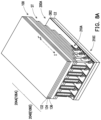
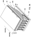
- FIG. 1 A through FIG. 4 C illustrate varying views of manufacturing a memory device in accordance with some embodiments.
- FIG. 5 A through FIG. 5 C illustrate varying views of a memory device in accordance with some embodiments.
- FIG. 6 A through FIG. 10 B illustrate varying views of manufacturing a memory device in accordance with some embodiments.
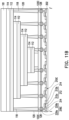
- FIG. 11 A and FIG. 11 B illustrate varying views of a memory device in accordance with some embodiments.
- FIG. 12 illustrates a method of forming a memory device in accordance with some embodiments.
- first and second features are formed in direct contact
- additional features may be formed between the first and second features, such that the first and second features may not be in direct contact
- present disclosure may repeat reference numerals and/or letters in the various examples. This repetition is for the purpose of simplicity and clarity and does not in itself dictate a relationship between the various embodiments and/or configurations discussed.
- spatially relative terms such as “beneath,” “below,” “lower,” “above,” “upper” and the like, may be used herein for ease of description to describe one element or feature's relationship to another element(s) or feature(s) as illustrated in the figures.
- the spatially relative terms are intended to encompass different orientations of the device in use or operation in addition to the orientation depicted in the figures.
- the apparatus may be otherwise oriented (rotated 180 degrees or at other orientations) and the spatially relative descriptors used herein may likewise be interpreted accordingly.
- the 3D memory device is a ferroelectric field effect transistor (FeFET) memory circuit including a plurality of vertically stacked memory cells.
- FeFET ferroelectric field effect transistor
- each memory cell is regarded as a FeFET that includes a word line region acting as a gate electrode, a bit line region acting as a first source/drain electrode, a source line region acting as a second source/drain electrode, a ferroelectric material acting as a gate dielectric, and an oxide semiconductor (OS) acting as a channel region.
- each memory cell is regarded as a thin film transistor (TFT).
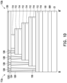
- FIG. 1 A through FIG. 4 C illustrate varying views of manufacturing a memory device in accordance with some embodiments.
- FIG. 1 B is illustrated along a reference cross-section I-I′ illustrated in FIG. 1 A
- FIG. 1 C is illustrated along a reference cross-section II-II′ illustrated in FIG. 1 A
- FIG. 1 D is illustrated along a reference cross-section III-III′ illustrated in FIG. 1 A
- FIG. 2 B through 4 B is illustrated along a reference cross-section I-I′ illustrated in FIG. 2 A through 4 A
- FIG. 2 C through 4 C is illustrated along a reference cross-section I-I′ illustrated in FIG. 2 A through 4 A .
- a memory 100 is formed over a carrier C 1 .
- a de-bonding layer DB 1 is formed on a top surface of the carrier C 1
- the memory 100 is formed on the de-bonding layer DB 1 .
- the carrier C 1 is a glass substrate and the de-bonding layer DB 1 is a light-to-heat conversion (LTHC) release layer formed on the glass substrate.
- LTHC light-to-heat conversion
- the disclosure is not limited thereto, and other suitable materials may be adapted for the carrier C 1 and the de-bonding layer DB 1 .
- a buffer layer (not shown) is coated on the de-bonding layer DB 1 , where the de-bonding layer DB 1 is sandwiched between the buffer layer and the carrier C 1 , and a top surface of the buffer layer further provides a high degree of coplanarity.
- the buffer layer may be a dielectric material layer or a polymer layer which is made of polyimide, BCB, PBO, or any other suitable polymer-based dielectric material.
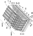
- the memory 100 (also referred to as a memory array) includes a plurality of memory cells 102 , which may be arranged in a grid of rows and columns.
- the memory cells 102 may be further stacked vertically to provide a three dimensional memory, thereby increasing device density.
- the memory 100 is a 3D stackable memory.
- the memory 100 may be a flash memory, such as a NAND flash memory, a NOR flash memory, or the like.
- a process temperature of the memory 100 is higher than 400° C., for example. In an embodiment, a process temperature of the memory 100 is about 550° C.
- a gate of each memory cell 102 is electrically coupled to a respective word line (e.g., conductive line 112 ), a first source/drain structure of each memory cell 102 is electrically coupled to a respective conductive line 126 A (e.g., bit line), and a second source/drain structure of each memory cell 102 is electrically coupled to a respective conductive line 126 B (e.g., source line).
- the memory cells 102 in a same horizontal row of the memory 100 may share a common word line while the memory cells 102 in a same vertical column of the memory 100 may share a common source line and a common bit line.
- the memory 100 includes a memory cell region 106 A and staircase regions 106 B, 106 C at opposite sides of the memory cell region 106 A.
- the memory cells 102 are disposed over an etching stop layer 101 in the memory cell region 106 A.
- the memory 100 may include a plurality of staircase structures ST in the memory cell region 106 A and the staircase regions 106 B, 106 C, and a dielectric material 104 is disposed between the staircase structures ST.
- the staircase structure ST includes a plurality of vertically stacked conductive lines 112 (e.g., word lines) with dielectric layers 114 disposed between adjacent ones of the conductive lines 112 .
- the conductive lines 112 and the dielectric layers 114 are stacked along a direction D from a first side to a second side.
- the first side is a bottom side and the second side is an upper side, and vice versa.
- the conductive lines 112 extend in a direction parallel to a major surface of the carrier C 1 .
- the conductive lines 112 may have a staircase configuration such that lower conductive lines 112 are longer than and extend laterally past endpoints of upper conductive lines 112 .
- FIG. 1 B multiple, stacked layers of conductive lines 112 are illustrated with topmost conductive lines 112 being the shortest and bottommost conductive lines 112 being the longest.
- Respective lengths of the conductive lines 112 may increase in a direction towards the underlying etching stop layer 101 . In this manner, a portion of each of the conductive lines 112 may be accessible from above the memory 100 , and conductive contacts may be made to exposed portions of the conductive lines 112 , respectively.
- the staircase structure ST is illustrated as contacting the etching stop layer 101 , any number of intermediate layers may be disposed between the etching stop layer 101 and the staircase structure ST. In alternative embodiments, the etching stop layer 101 is omitted.
- the conductive line 112 may each include two barrier layers (not shown) and a metal layer between the barrier layers. Specifically, a barrier layer is disposed between the metal layer and the adjacent dielectric layer 114 . The barrier layers may prevent the metal layer from diffusion to the adjacent dielectric layers 114 . The barrier layers may also provide the function of increasing the adhesion between the metal layer and the adjacent dielectric layers 114 , and may be referred to as glue layers in some examples. In some embodiments, both barrier layers and glue layers with different materials are provided as needed.
- the barrier layers are formed of a first conductive material, such as a metal nitride, such as titanium nitride, tantalum nitride, molybdenum nitride, zirconium nitride, hafnium nitride, or the like.
- the metal layer may be formed of a second conductive material, such as a metal, such as tungsten, ruthenium, molybdenum, cobalt, aluminum, nickel, copper, silver, gold, alloys thereof, or the like.
- the barrier layers and metal layer may each be formed by an acceptable deposition process such as CVD, PVD, ALD, PECVD, or the like.
- the memory 100 further includes conductive pillars 116 A (e.g., electrically connected to bit lines) and conductive pillars 116 B (e.g., electrically connected to source lines) arranged alternately.
- the conductive pillars 116 A and 116 B may each extend in a direction perpendicular to the conductive lines 112 .
- a dielectric material 115 is disposed between and isolates adjacent ones of the conductive pillars 116 A and the conductive pillars 116 B, and a dielectric material 117 is disposed between and isolates adjacent pairs of the conductive pillars 116 A and 116 B.
- a material of the conductive pillars 116 A, 116 B may include copper, titanium, titanium nitride, tantalum, tantalum nitride, tungsten, ruthenium, aluminum, combinations thereof, or the like, which may be formed by a deposition process (e.g., CVD, ALD, PVD, PECVD, or the like) and a planarization (e.g., a CMP, etch back, or the like).
- the conductive pillars 116 A correspond to and are electrically connected to the bit lines in the memory device
- the conductive pillars 116 B correspond to correspond to and are electrically connected to the source lines in the memory 100 .
- the conductive pillars 116 A correspond to and are electrically connected to the source lines in the memory device
- the conductive pillars 116 B correspond to correspond to and are electrically connected to the bit lines in the memory 100 .
- the staircase configuration of the conductive lines 112 are disposed in the staircase regions 106 B, 106 C, and the conductive pillars 116 A and 116 B are disposed in the memory cell region 106 A. Pairs of the conductive pillars 116 A and 116 B along with an intersecting conductive line 112 define boundaries of each memory cell 102 , and the dielectric material 117 is disposed between and isolates adjacent pairs of the conductive pillars 116 A and 116 B. In some embodiments, the conductive pillars 116 B are electrically coupled to ground.
- the memory device is formed by a “staircase first process” in which the staircase structure is formed before the memory cells are formed.
- the disclosure is not limited thereto.
- the memory device may be formed by a “staircase last process” in which the staircase structure is formed after the memory cells are formed.
- a plurality of conductive contacts 118 are formed to electrically connected to the conductive lines 112 respectively.
- the conductive contacts 118 may be formed in a dielectric material 120 over the dielectric material 104 . Top surfaces of the conductive contacts 118 may be substantially coplanar with top surfaces of the conductive pillars 116 A and 116 B, the dielectric layers 114 and the dielectric materials 104 , 115 and 117 . Then, a plurality of conductive contacts 122 A, 122 B and 122 C are formed on and electrically connected to the conductive pillars 116 A, the conductive pillars 116 B, and the conductive contacts 118 , respectively.
- the conductive contacts 122 A, 122 B and 122 C may be formed in a dielectric material 124 over the dielectric material 120 .
- the conductive material of the conductive contacts 122 A, 122 B and 122 C may include copper, a copper alloy, silver, gold, tungsten, cobalt, aluminum, nickel, or the like.
- a plurality of conductive lines 126 A, 126 B are formed to electrically connect to the conductive contacts 122 A and 122 B, so as to electrically connect to the conductive pillars 116 A and 116 B.
- the conductive lines 126 A, 126 B are crossing over the plurality of the conductive lines 112 and the dielectric layers 114 .
- Conductive contacts 128 are formed to electrically connect to the conductive contacts 122 C, so as to electrically connect to the conductive lines 112 .
- the conductive lines 126 A and the conductive lines 126 B may each extend in a direction perpendicular to the conductive lines 112 .
- the conductive lines 126 A are electrically connected to the conductive pillars 116 A through the conductive contacts 122 A, and the conductive lines 126 B are electrically connected to the conductive pillars 116 B through the conductive contacts 122 B. Although the conductive lines 126 A and the conductive lines 126 B are arranged as shown in FIG. 1 A , the conductive lines 126 A and the conductive lines 126 B may have any suitable arrangement.
- the conductive contacts 128 are electrically connected to the conductive lines 112 through the conductive contacts 118 and 122 C. The conductive lines 126 A, 126 B and the conductive contacts 128 may be formed simultaneously.
- the conductive lines 126 A, 126 B and the conductive contacts 128 are formed in a dielectric material 130 over the dielectric material 124 , for example.
- the conductive line 126 A and the corresponding conductive contact 122 A are integrally formed
- the conductive line 126 B and the corresponding conductive contact 122 B are integrally formed and/or the conductive contacts 128 and the conductive contacts 122 C are integrally formed.
- the conductive lines 126 A, 126 B and the conductive contacts 122 A and 122 B are formed by using a dual damascene process
- the conductive contacts 128 and the conductive contacts 122 C are formed by in a same process.
- the conductive contact 128 is also referred to as a pad portion, and the conductive contact 122 C is also referred to as a via portion.
- a width of the conductive contacts 128 is may be larger than a width of the conductive contacts 122 C.
- the conductive contact 128 may be also referred to as a bonding pad, the dielectric material 130 aside the conductive contact 128 may be also referred to as a bonding layer, and the conductive contact 128 and the dielectric material 130 may be also collectively referred to as a bonding structure.
- the conductive contact 122 C may be also referred to as a bonding via.
- a material of the conductive lines 126 A, 126 B and the conductive contacts 128 includes copper, silver, gold, tungsten, aluminum, combinations thereof, or the like, for example.
- the dielectric materials 104 , 115 , 117 , 120 , 124 and 130 may include an oxide (e.g., silicon oxide or the like), a nitride (e.g., silicon nitride or the like), phospho-silicate glass (PSG), boro-silicate glass (BSG), boron-doped phospho-silicate glass (BPSG), undoped silicate glass (USG), a combination thereof or the like.
- the memory 100 includes a channel layer 108 .
- the channel layer 108 may provide channel regions for the memory cells 102 .
- an appropriate voltage e.g., higher than a respective threshold voltage (V th ) of a corresponding memory cell 102
- V th a respective threshold voltage
- the channel layer 108 includes materials suitable for providing channel regions for the memory cells 102 .
- the channel layer 108 includes oxide semiconductor (OS) such as zinc oxide (ZnO), indium tungsten oxide (InWO), indium gallium zinc oxide (InGaZnO, IGZO), indium zinc oxide (InZnO), indium tin oxide (ITO), combinations thereof, or the like.
- OS oxide semiconductor
- the channel layer 108 includes polycrystalline silicon (poly-Si), amorphous silicon (a-Si), or the like.
- the channel layer 108 may be deposited by CVD, PVD, ALD, PECVD, or the like.
- a memory material layer 110 is disposed between the channel layer 108 and each of the conductive lines 112 and the dielectric layer 114 , and the memory material layer 110 serve as a gate dielectric for each memory cell 102 .
- the memory material layer 110 includes a ferroelectric material, such as a hafnium oxide, hafnium zirconium oxide, silicon-doped hafnium oxide, or the like.
- the memory material layer 110 may be polarized in one of two different directions, and the polarization direction may be changed by applying an appropriate voltage differential across the memory material layer 110 and generating an appropriate electric field.
- the polarization may be relatively localized (e.g., generally contained within each boundaries of the memory cells 102 ), and a continuous region of the memory material layer 110 may extend across a plurality of memory cells 102 .
- a threshold voltage of a corresponding memory cell 102 varies, and a digital value (e.g., 0 or 1) can be stored.
- the corresponding memory cell 102 when a region of the memory material layer 110 has a first electrical polarization direction, the corresponding memory cell 102 may have a relatively low threshold voltage, and when the region of the memory material layer 110 has a second electrical polarization direction, the corresponding memory cell 102 may have a relatively high threshold voltage.
- the difference between the two threshold voltages may be referred to as the threshold voltage shift.
- a larger threshold voltage shift makes it easier (e.g., less error prone) to read the digital value stored in the corresponding memory cell 102 .
- a write voltage is applied across a portion of the memory material layer 110 corresponding to the memory cell 102 .
- the write voltage is applied, for example, by applying appropriate voltages to a corresponding conductive line 112 (e.g., the word line) and the corresponding conductive pillars 116 A/ 116 B (e.g., the bit line/source line).
- a polarization direction of the region of the memory material layer 110 may be changed.
- the corresponding threshold voltage of the corresponding memory cell 102 may also be switched from a low threshold voltage to a high threshold voltage or vice versa, and a digital value may be stored in the memory cell 102 . Because the conductive lines 112 intersect the conductive pillars 116 A and 116 B, individual memory cells 102 may be selected for the write operation.
- a read voltage (a voltage between the low and high threshold voltages) is applied to the corresponding conductive line 112 (e.g., the word line).
- the memory cell 102 may or may not be turned on.
- the conductive pillar 116 A may or may not be discharged through the conductive pillar 116 B (e.g., a source line that is coupled to ground), and the digital value stored in the memory cell 102 can be determined. Because the conductive lines 112 intersect the conductive pillars 116 A and 116 B, individual memory cells 102 may be selected for the read operation.
- the staircase shape of the conductive lines 112 provides a surface on each of the conductive lines 112 for the conductive contact 122 C to land on.
- the conductive line 112 has opposite sides 112 a and 112 b , and the conductive contact 122 C for the conductive line 112 are disposed on one of the sides 112 a and 112 b .
- the conductive contact 122 C for the conductive line 112 is disposed at one of the sides 112 a and 112 b .
- the conductive contacts 122 C for the conductive line 112 are disposed at both sides 112 a and 112 b .
- the conductive contacts 122 C for the staircase structure ST are disposed at the same side 112 a of the conductive lines 112 .
- the opposite sides 112 a and 112 b are also referred to as opposite sides of the memory cell region 106 A or opposite sides of the staircase structure ST.
- the staircase structure ST includes a staircase ST 1 in the staircase region 106 B and a staircase ST 2 in the staircase region 106 C. In an embodiment in which the memory 100 is a single-sided driving structure, one of the staircases ST 1 and ST 2 is used, and the other of the staircases ST 1 and ST 2 is non-used.
- the used staircase may be also referred to as a used staircase
- the non-used staircase may be also referred to as a non-used staircase.
- the conductive contacts 122 C are all disposed on the to the staircases ST 1
- the staircases ST 1 are used staircases
- the staircases ST 2 are non-used staircases.
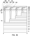
- a circuit structure 200 is formed over a carrier C 2 .
- the circuit structure 200 is also referred to as a periphery circuit.
- a process temperature of the circuit structure 200 is lower than 400° C., for example.
- the circuit structure 200 includes a plurality of drivers 210 A, 210 B and 210 C.
- the drivers 210 A, 210 B and 210 C may be formed on and in a substrate 202 .
- the substrate 202 may be a semiconductor substrate, such as a wafer, a bulk semiconductor, a semiconductor-on-insulator (SOI) substrate, or the like, which may be doped (e.g., with a p-type or an n-type dopant) or undoped.
- SOI substrate is a layer of a semiconductor material formed on an insulator layer.
- the insulator layer may be, for example, a buried oxide (BOX) layer, a silicon oxide layer, or the like.
- the insulator layer is provided on a substrate, typically a silicon or glass substrate. Other substrates, such as a multi-layered or gradient substrate may also be used.
- the semiconductor material of the substrate 202 may include silicon; germanium; a compound semiconductor including silicon carbide, gallium arsenide, gallium phosphide, indium phosphide, indium arsenide, and/or indium antimonide; an alloy semiconductor including silicon-germanium, gallium arsenide phosphide, aluminum indium arsenide, aluminum gallium arsenide, gallium indium arsenide, gallium indium phosphide, and/or gallium indium arsenide phosphide; or combinations thereof.
- the drivers 210 A, 210 B and 210 C may include transistors.
- the drivers 210 A, 210 B and 210 C respectively include a gate structure 212 and a source/drain structure 214 on opposite sides of the gate structure 212 .
- the gate structure 212 may include a gate dielectric layer 212 a over a top surface of the substrate 202 , a gate electrode 212 b over the gate dielectric layer 212 a and a gate spacer 212 c formed along a sidewall of the gate dielectric layer 212 a and the gate electrode 212 b .
- the source/drain structure 214 is a doping region in the substrate 202 or an epitaxial structure formed in a recess of the substrate 202 .
- the gate spacer 212 c may separate the source/drain structure 214 from the gate electrode 212 b by appropriate lateral distances.
- the transistors of the drivers 210 A, 210 B and 210 C are referred as planar-type transistors, and skin portions of the substrate 202 respectively covered by the gate structure 212 and extending between the source/drain structures 214 is functioned as a conductive channel of the transistor.
- an isolation structure 204 such as shallow trench isolation (STI) is formed between the transistors of the drivers 210 A, 210 B and 210 C.
- a well (not shown) may be formed between the isolation structures 204 , and the source/drain structure 214 is formed in the well.
- the transistors of the drivers 210 A, 210 B and 210 C are respectively formed as a fin-type transistor or a gate-all-around (GAA) transistor.
- GAA gate-all-around
- three-dimensional structure(s) e.g., fin structure(s), nanosheet(s) or the like
- FIG. 2 A , FIG. 2 B and FIG. 2 C discuss transistors formed on and in the substrate 202 , other active devices (e.g., diodes or the like) and/or passive devices (e.g., capacitors, resistors, or the like) may also be formed as part of the circuit structure 200 .
- the circuit structure 200 in addition to the memory circuit, the circuit structure 200 further includes logic circuits, sense amplifiers, controllers, input/output circuits, image sensor circuits, the like, or combinations thereof.
- the drivers 210 A, 210 B and 210 C are disposed corresponding to the conductive lines 126 A, 126 B and 112 , respectively. A number of the drivers 210 A, 210 B and 210 C may be respectively the same as the conductive lines 126 A, 126 B and 112 .
- the substrate 202 may include a region 204 A corresponding to the memory cell region 106 A and a region 204 B corresponding to one of the staircase region 106 B and 106 C.
- the second region 204 B corresponds to one of the staircase regions 106 B and 106 C.
- the second region 204 B corresponds to the staircase region 106 B.
- the drivers 210 A and 210 B are disposed in the region 204 A, and the drivers 210 C are disposed in the region 204 B.
- a shown in FIG. 2 A at least two of the drivers 210 A and 210 B are disposed adjacent to each other.
- the drivers 210 A are disposed immediately adjacent to each other
- the drivers 210 B are disposed immediately adjacent to each other
- the driver 210 A and the driver 210 B are disposed immediately adjacent to each other.
- the drivers 210 A and 210 B may have any suitable arrangement.
- the drivers 210 C may be arranged in a grid of rows and columns.
- a number of the rows of the drivers 210 C is the same as a number of the staircase structures ST, and a number of the columns of the drivers 210 C is the same as a number of the conductive lines 112 of one staircase structure ST.
- the drivers 210 A and 210 B may be alternately arranged. In some embodiments, a spacing between adjacent transistors of the drivers 210 C and between adjacent transistors of drivers 210 A and 210 B ranges from 10 nm to 1000 nm. Furthermore, although not shown, the drivers 210 A, 210 B and 210 C may further include other active device(s) and/or passive device(s).
- a dielectric material 216 may surrounds and isolates the gate dielectric layers 212 a and the gate electrodes 212 b .
- a plurality of conductive contacts 218 A, 218 B and 218 C are formed on and electrically connected to the drivers 210 A, 210 B and 210 C, respectively.
- the conductive contacts 218 A, 218 B and 218 C are formed to electrically connected to the source/drain structures 214 of the drivers 210 A, 210 B and 210 C.
- the conductive contacts 218 A, 218 B and 218 C may be also referred to as source/drain contacts.
- the conductive contacts 218 A, 218 B and 218 C are formed in the dielectric material 216 .
- the conductive contacts 218 A, 218 B and 218 C respectively include a pad portion 220 a and a via portion 220 b between the pad portion 220 a and the driver 210 A, 210 B or 210 C.
- the pad portion 220 a may have a width lager than the via portion 220 b .
- the pad portion 220 a is also referred to as a bonding pad
- the via portion 220 b is also referred to as a bonding via
- the dielectric material 216 is also referred to as a bonding layer
- the pad portion 220 a , the via portion 220 b and the dielectric material 216 may be also collectively referred to as a bonding structure.
- the memory 100 and the circuit structure 200 are bonded.
- the memory 100 is de-bonded and is separated from the carrier C 1 .
- the de-bonding process includes projecting a light such as a laser light or an UV light on the de-bonding layer DB 1 (e.g., the LTHC release layer) so that the carrier C 1 can be easily removed along with the de-bonding layer DB 1 .
- a tape (not shown) may be used to secure the structure before de-bonding the carrier C 1 and the de-bonding layer DB 1 .
- the memory 100 is bonded onto the circuit structure 200 through a wafer to wafer bonding process, for example.
- the conductive lines 126 A are bonded to the conductive contacts 218 A of the drivers 210 A
- the conductive lines 126 B are bonded to the conductive contacts 218 B of the drivers 210 B
- the conductive contacts 128 of the conductive lines 112 are bonded to the conductive contacts 218 C of the drivers 210 C.
- the conductive lines 126 A are electrically connected to the drivers 210 A
- the conductive lines 126 B are electrically connected to the drivers 210 B
- the conductive lines 112 are electrically connected to the drivers 210 C, respectively.
- the dielectric material 130 may be bonded to the dielectric material 216 .
- the conductive lines 126 A connecting to the adjacent drivers 210 A may be physically separated by at least one conductive line 126 A, 126 B therebetween.
- the conductive lines 126 A, 126 B connecting to the adjacent drivers 210 A, 210 B are physically separated by two conductive lines 126 A, 126 B therebetween.
- the drivers 210 A and the drivers 210 B may have any suitable arrangement.
- the conductive lines 126 A, 126 B connecting to the adjacent drivers 210 A, 210 B are immediately adjacent to each other or physically separated by one or more conductive lines 126 A, 126 B therebetween.
- a reflow process may be performed. During the bonding process, a process temperature may be lower than 400° C.
- the de-bonding process includes projecting a light such as a laser light or an UV light on the de-bonding layer DB 2 (e.g., the LTHC release layer) so that the carrier C 2 can be easily removed along with the de-bonding layer DB 2 .
- a tape (not shown) may be used to secure the structure before de-bonding the carrier C 2 and the de-bonding layer DB 2 .
- a thinning process such as a grinding process is performed on the substrate 202 after de-bonding from the carrier C 2 , so as to reduce a total thickness of the formed structure.
- the memory 100 is bonded onto the circuit structure 200 over the carrier C 2 , and then the resulting structure is de-bonded from the carrier C 2 .
- the disclosure is not limited thereto.
- the circuit structure 200 is bonded onto the memory 100 over the carrier C 1 .
- the resulting structure is de-bonded from the carrier C 1 , to form the memory device 10 as shown in FIG. 4 A , FIG. 4 B and FIG. 4 C .
- a thinning process such as a grinding process is performed on the substrate 202 after bonding the circuit structure 200 to the memory 100 , so as to reduce a total thickness of the formed structure.
- the memory 100 and the circuit structure 200 are formed separately and then combined by bonding.
- the memory 100 and the circuit structure 200 may be formed under different process condition such as process temperature, and one would not have an impact on the other.
- the memory 100 without the periphery circuit is fabricated under a relative high temperature such as 550° C. which may have impact on the circuit structure 200 , however, the impact is prevented since the memory 100 and the circuit structure 200 are formed separately. Accordingly, the memory and the circuit structure may be formed under the desired condition thereof, and the performance of the formed memory device is improved.
- the circuit structure 200 is formed at one side of the memory 100 .
- the drivers 210 A, 210 B and 210 C are all disposed below or above the memory 100 .
- the disclosure is not limited thereto.
- the drivers 210 A, 210 B and 210 C are formed at different sides of the memory 100 .
- FIG. 6 A through FIG. 10 B illustrate varying views of manufacturing a memory device in accordance with some embodiments.
- FIG. 6 B and FIG. 6 C are illustrated along reference cross-sections I-I′ and II-II′ illustrated in FIG. 6 A .
- FIG. 8 B through FIG. 10 B are illustrated along reference cross-sections III-III′ illustrated in FIG. 8 A through FIG. 10 A .
- the manufacturing method is similar to the patterning method of FIG. 1 A to FIG. 4 A and FIG. 1 B to FIG. 4 B , and the main difference is described as below.
- a memory 100 is formed over a carrier C 1 .
- the structure, the material and the forming process of the memory 100 are similar to those of the memory 100 as described with reference to FIG. 1 A , FIG. 1 B , FIG. 1 C and FIG. 1 D , and the main difference lies in the conductive lines 126 A and the conductive lines 126 B are formed at opposite sides (i.e., upper side and bottom side) of the staircase structures ST.
- the conductive lines 126 A are disposed over the staircase structures ST, and the conductive lines 126 B are disposed below the staircase structures ST.
- FIG. 6 A the conductive lines 126 A are disposed over the staircase structures ST
- the conductive lines 126 B are disposed below the staircase structures ST.
- the conductive pillars 116 B are extended into the etching stop layer 101 , to electrically connect to the conductive lines 126 B.
- the conductive contacts 122 B, 122 B′ in dielectric materials 134 , 136 are disposed between the conductive lines 126 B and the conductive pillars 116 B to electrically connect the conductive lines 126 B and the conductive pillars 116 B.
- the conductive lines 126 B electrically connect the conductive pillars 116 B in the same row, for example.
- the conductive contacts 122 B′ are disposed between the conductive pillars 116 B and the conductive contacts 122 B.
- one of the conductive contact 122 B and the corresponding conductive contact 122 B′ is omitted, or the conductive contact 122 B and the corresponding conductive contact 122 B′ are formed integrally.
- the conductive lines 126 B below the staircase structures ST may have other configurations.
- the conductive lines 126 A are bit lines, and the conductive lines 126 B are source lines.
- the conductive lines 126 A are source lines, and the conductive lines 126 B are bit lines.
- the memory 100 may be formed by the following steps. First, the conductive lines 126 B in a dielectric material 132 are formed over the de-bonding layer DB 1 , and the conductive contacts 122 B and the conductive contacts 122 B′ are formed over the conductive lines 126 B. For example, the conductive contacts 122 B are formed in a dielectric material 134 and the conductive contacts 122 B′ are formed in a dielectric material 136 . Then, the etching stop layer 101 is formed over the dielectric material 136 . After that, the conductive lines 112 , the conductive pillars 116 A and the conductive pillars 116 B may be formed over the etching stop layer 101 .
- the conductive pillars 116 B are formed to extend into the etching stop layer 101 while the conductive pillars 116 A are formed to stop on the top surface of the etching stop layer 101 .
- the conductive contacts 122 A and the conductive contacts 122 C may be formed in the dielectric material 124 to electrically connect to the conductive pillars 126 A and the conductive contacts 118 , respectively.
- the conductive lines 126 A and the conductive contacts 128 may be formed to electrically connect to the conductive contacts 122 A and the conductive contacts 122 C, respectively.
- a circuit structure 200 A is formed over a carrier C 2
- a circuit structure 200 B is formed over a carrier C 2 ′.
- the circuit structure 200 A may include a plurality of drivers 210 A and a plurality drivers 210 C.
- the circuit structure 200 A may include a plurality of drivers 210 B.
- the structure, the material and the forming process of the drivers 210 A, 210 B and 210 C are similar to those of the drivers 210 A, 210 B and 210 C as described with reference to FIG. 2 B and FIG. 3 B , and the main difference lies in the drivers 210 B are formed over the carrier C 2 ′ different from the carrier C 2 over which the drivers 210 A and 210 C are formed.
- the fabricating process of the drivers 210 A and 210 C and the fabricating process of the drivers 210 B are separately performed.
- the memory 100 of FIG. 6 A is bonded to one of the circuit structure 200 A and the circuit structure 200 B.
- the memory 100 is de-bonded and separated from the carrier C 1 , and then the memory 100 is bonded to the circuit structure 200 A over the carrier C 2 .
- the memory 100 is bonded onto the circuit structure 200 A through a wafer to wafer bonding process, for example.
- the conductive lines 126 A are bonded to the conductive contacts 218 A of the drivers 210 A, and the conductive contacts 128 of the conductive lines 112 are bonded to the conductive contacts 218 C of the drivers 210 C, and the dielectric material 130 is bonded to the dielectric material 216 .
- the conductive lines 126 A are electrically connected to the drivers 210 A, and the conductive lines 112 are electrically connected to the drivers 210 C, respectively.
- a reflow process may be performed.
- a process temperature may be lower than 400° C.
- a thinning process such as a grinding process is performed on the substrate 202 after de-bonding from the carrier C 2 , so as to reduce a total thickness of the formed structure.
- the circuit structure 200 B is bonded to the resulting structure of FIG. 8 A and FIG. 8 B .
- the circuit structure 200 B is de-bonded and separated from the carrier C 2 ′, and then the circuit structure 200 B is bonded to the memory 100 over the carrier C 2 .
- the circuit structure 200 B is bonded onto the memory 100 through a wafer to wafer bonding process, for example.
- the conductive contacts 218 B of the drivers 210 B are bonded to the conductive lines 126 B, and a dielectric material 216 aside the conductive contacts 218 B is bonded to the dielectric material 132 aside the conductive lines 126 B.
- the conductive lines 126 B are electrically connected to the drivers 210 B, respectively.
- a reflow process may be performed.
- a process temperature may be lower than 400° C.
- a thinning process such as a grinding process is performed on the substrate 202 after de-bonding from the carrier C 2 ′, so as to reduce a total thickness of the formed structure.
- the circuit structure 200 B is bonded to the memory 100 after bonding the circuit structure 200 A onto the memory 100 . In alternative embodiments, the circuit structure 200 B is bonded to the memory 100 before bonding the circuit structure 200 A onto the memory 100 .
- the formed structure of FIG. 9 A and FIG. 9 B is de-bonded from the carrier C 1 , to form a memory device 10 .
- the de-bonding process includes projecting a light such as a laser light or an UV light on the de-bonding layer DB 1 (e.g., the LTHC release layer) so that the carrier C 1 can be easily removed along with the de-bonding layer DB 1 .
- a tape (not shown) may be used to secure the structure before de-bonding the carrier C 1 and the de-bonding layer DB 1 .
- all drivers connecting to the same type of the conductive lines are formed over the same carrier.
- the drivers 210 A connecting to the conductive lines 126 A are all formed over the carrier C 2
- the drivers 210 B connecting to the conductive lines 126 B are all formed over the carrier C 2
- the drivers 210 C connecting to the conductive lines 112 are all formed over the carrier C 2 ′.
- the disclosure is not limited thereto.
- drivers connecting to different type of the conductive lines are formed over the same carrier. That is, two of the driver 210 A, driver 210 B and the driver 210 C may be formed over the same carrier.
- FIG. 1 A through FIG. 10 B illustrate a particular pattern for the conductive pillars 116 A and 116 B
- the conductive pillars 116 A and 116 B have a staggered pattern.
- the conductive pillars 116 A and 116 B in a same row of the array are all aligned with each other.
- the memory device is a single-sided driving structure, and the second region 204 B corresponds to one of the staircase regions 106 B and 106 C.
- the memory device 10 is a double-sided driving structure, the second regions 204 B at opposite sides of the first region 204 A correspond to the staircase region 106 B and the staircase region 106 C respectively.
- the conductive contacts 118 are formed at both sides 112 a and 112 b of the conductive line 112 , and the drivers 210 C are disposed in both the second regions 204 B to electrically connect the conductive contacts 118 respectively.
- a number of the drivers 210 C is doubled.
- FIG. 12 illustrates a method of forming a memory device in accordance with some embodiments.
- the method is illustrated and/or described as a series of acts or events, it will be appreciated that the method is not limited to the illustrated ordering or acts. Thus, in some embodiments, the acts may be carried out in different orders than illustrated, and/or may be carried out concurrently. Further, in some embodiments, the illustrated acts or events may be subdivided into multiple acts or events, which may be carried out at separate times or concurrently with other acts or sub-acts. In some embodiments, some illustrated acts or events may be omitted, and other un-illustrated acts or events may be included.
- a three dimensional memory is formed over a first carrier, the three dimensional memory including a plurality of first conductive lines.
- FIGS. 1 A, 1 B, 1 C, 1 D, 6 A and 6 B illustrate varying views corresponding to some embodiments of act S 300 .
- a first circuit structure is formed over a second carrier, the first circuit structure including a plurality of first drivers and a plurality of first bonding pads electrically connected to the plurality of first drivers respectively.
- FIGS. 2 A, 2 B, 2 C, 7 A and 7 B illustrate varying views corresponding to some embodiments of act S 302 .
- FIGS. 3 A, 3 B, 3 C, 5 A, 5 B, 5 C, 8 A, 8 B, 9 A and 9 B illustrate varying views corresponding to some embodiments of act S 304 .
- the memory and the circuit structure are formed separately and then combined by bonding.
- the memory and the circuit structure may be formed under a desired condition thereof such as a desired process temperature, and one would not have an impact on the other. Accordingly, the performance of the formed memory device is improved.
- a memory device includes a staircase structure, a plurality of first conductive contacts, a plurality of first drivers and a plurality of second conductive contacts.
- the staircase structure includes a plurality of first conductive lines and a plurality of first dielectric layers stacked alternately.
- the first conductive contacts are electrically connected to the plurality of first conductive lines respectively.
- the second conductive contacts are electrically connected to the plurality of first drivers respectively.
- the plurality of first conductive contacts and the plurality of second conductive contacts are bonded and disposed between the plurality of first conductive lines and the plurality of first drivers.
- a memory device includes a staircase structure, a plurality of first drivers, a plurality of second conductive lines and a plurality of second drivers.
- the staircase structure has a first side and a second side opposite to the first side and includes a plurality of first conductive lines and a plurality of first dielectric layers stacked alternately along a direction from the first side to the second side.
- the first drivers are disposed at the first side of the staircase structure and electrically connected to the plurality of first conductive lines respectively.
- the second conductive lines are disposed at the second side and cross over the plurality of first conductive lines and the plurality of dielectric layers.
- the second drivers are disposed at the second side of the staircase structure and electrically connected to the second conductive lines respectively.
- a method of forming a memory device includes following steps.
- a three dimensional memory is formed over a first carrier and the three dimensional memory includes a plurality of first conductive lines.
- a first circuit structure is formed over a second carrier, and the first circuit structure includes a plurality of first drivers and a plurality of first bonding pads electrically connected to the plurality of first drivers respectively.
- the three dimensional memory and the first circuit structure are electrically connected by bonding the plurality of first conductive lines and the plurality of the first bonding pads.
Landscapes
- Semiconductor Memories (AREA)
- Engineering & Computer Science (AREA)
- Manufacturing & Machinery (AREA)
- Dram (AREA)
Abstract
Description
Claims (20)
Priority Applications (4)
| Application Number | Priority Date | Filing Date | Title |
|---|---|---|---|
| US17/344,946 US12051663B2 (en) | 2021-01-15 | 2021-06-11 | Memory devices and methods of forming the same |
| TW111100511A TW202230745A (en) | 2021-01-15 | 2022-01-06 | Memory devices |
| CN202210030442.5A CN114361179A (en) | 2021-01-15 | 2022-01-12 | Memory device and method of forming the same |
| US18/751,336 US20240347489A1 (en) | 2021-01-15 | 2024-06-23 | Memory devices |
Applications Claiming Priority (2)
| Application Number | Priority Date | Filing Date | Title |
|---|---|---|---|
| US202163137757P | 2021-01-15 | 2021-01-15 | |
| US17/344,946 US12051663B2 (en) | 2021-01-15 | 2021-06-11 | Memory devices and methods of forming the same |
Related Child Applications (1)
| Application Number | Title | Priority Date | Filing Date |
|---|---|---|---|
| US18/751,336 Division US20240347489A1 (en) | 2021-01-15 | 2024-06-23 | Memory devices |
Publications (2)
| Publication Number | Publication Date |
|---|---|
| US20220230976A1 US20220230976A1 (en) | 2022-07-21 |
| US12051663B2 true US12051663B2 (en) | 2024-07-30 |
Family
ID=81108928
Family Applications (2)
| Application Number | Title | Priority Date | Filing Date |
|---|---|---|---|
| US17/344,946 Active 2041-07-23 US12051663B2 (en) | 2021-01-15 | 2021-06-11 | Memory devices and methods of forming the same |
| US18/751,336 Pending US20240347489A1 (en) | 2021-01-15 | 2024-06-23 | Memory devices |
Family Applications After (1)
| Application Number | Title | Priority Date | Filing Date |
|---|---|---|---|
| US18/751,336 Pending US20240347489A1 (en) | 2021-01-15 | 2024-06-23 | Memory devices |
Country Status (3)
| Country | Link |
|---|---|
| US (2) | US12051663B2 (en) |
| CN (1) | CN114361179A (en) |
| TW (1) | TW202230745A (en) |
Families Citing this family (1)
| Publication number | Priority date | Publication date | Assignee | Title |
|---|---|---|---|---|
| US11696449B2 (en) * | 2021-04-16 | 2023-07-04 | Taiwan Semiconductor Manufacturing Company, Ltd. | Semiconductor devices and methods of manufacturing thereof |
Citations (7)
| Publication number | Priority date | Publication date | Assignee | Title |
|---|---|---|---|---|
| US20200027509A1 (en) * | 2018-07-20 | 2020-01-23 | Yangtze Memory Technologies Co., Ltd. | Three-dimensional memory devices |
| US20200144242A1 (en) * | 2018-11-06 | 2020-05-07 | Samsung Electronics Co.. Ltd. | Semiconductor device |
| US20200203364A1 (en) * | 2018-12-24 | 2020-06-25 | Sandisk Technologies Llc | Three-dimensional memory devices having a multi-stack bonded structure using a logic die and multiple three-dimensional memory dies and method of making the same |
| US20200335487A1 (en) * | 2019-03-01 | 2020-10-22 | Sandisk Technologies Llc | Three-dimensional memory device having an epitaxial vertical semiconductor channel and method for making the same |
| US20210066282A1 (en) * | 2019-09-02 | 2021-03-04 | Samsung Electronics Co., Ltd. | Three-dimensional semiconductor memory device |
| US20210082865A1 (en) * | 2019-03-01 | 2021-03-18 | Sandisk Technologies Llc | Methods for reusing substrates during manufacture of a bonded assembly including a logic die and a memory die |
| US20210407980A1 (en) * | 2020-06-29 | 2021-12-30 | Taiwan Semiconductor Manufacturing Co., Ltd. | 3D Semiconductor Package Including Memory Array |
-
2021
- 2021-06-11 US US17/344,946 patent/US12051663B2/en active Active
-
2022
- 2022-01-06 TW TW111100511A patent/TW202230745A/en unknown
- 2022-01-12 CN CN202210030442.5A patent/CN114361179A/en active Pending
-
2024
- 2024-06-23 US US18/751,336 patent/US20240347489A1/en active Pending
Patent Citations (7)
| Publication number | Priority date | Publication date | Assignee | Title |
|---|---|---|---|---|
| US20200027509A1 (en) * | 2018-07-20 | 2020-01-23 | Yangtze Memory Technologies Co., Ltd. | Three-dimensional memory devices |
| US20200144242A1 (en) * | 2018-11-06 | 2020-05-07 | Samsung Electronics Co.. Ltd. | Semiconductor device |
| US20200203364A1 (en) * | 2018-12-24 | 2020-06-25 | Sandisk Technologies Llc | Three-dimensional memory devices having a multi-stack bonded structure using a logic die and multiple three-dimensional memory dies and method of making the same |
| US20200335487A1 (en) * | 2019-03-01 | 2020-10-22 | Sandisk Technologies Llc | Three-dimensional memory device having an epitaxial vertical semiconductor channel and method for making the same |
| US20210082865A1 (en) * | 2019-03-01 | 2021-03-18 | Sandisk Technologies Llc | Methods for reusing substrates during manufacture of a bonded assembly including a logic die and a memory die |
| US20210066282A1 (en) * | 2019-09-02 | 2021-03-04 | Samsung Electronics Co., Ltd. | Three-dimensional semiconductor memory device |
| US20210407980A1 (en) * | 2020-06-29 | 2021-12-30 | Taiwan Semiconductor Manufacturing Co., Ltd. | 3D Semiconductor Package Including Memory Array |
Also Published As
| Publication number | Publication date |
|---|---|
| TW202230745A (en) | 2022-08-01 |
| CN114361179A (en) | 2022-04-15 |
| US20220230976A1 (en) | 2022-07-21 |
| US20240347489A1 (en) | 2024-10-17 |
Similar Documents
| Publication | Publication Date | Title |
|---|---|---|
| US11056454B2 (en) | Stacked three-dimensional heterogeneous memory devices and methods for forming the same | |
| US12293999B2 (en) | 3D semiconductor package including memory array | |
| US12002534B2 (en) | Memory array word line routing | |
| US12225731B2 (en) | Memory array contact structures | |
| US12363907B2 (en) | Memory device comprising conductive pillars | |
| US11605593B2 (en) | Semiconductor devices having interposer structure with adhesive polymer and methods for forming the same | |
| US12232328B2 (en) | Memory devices | |
| US20240215255A1 (en) | Method for fabricating memory device | |
| US11844224B2 (en) | Memory structure and method of forming the same | |
| US12538475B2 (en) | Drain sharing for memory cell thin film access transistors and methods for forming the same | |
| US12114506B2 (en) | Semiconductor structure and method of fabricating the same | |
| US20250240965A1 (en) | Memory device | |
| US20240347489A1 (en) | Memory devices | |
| US20250311242A1 (en) | Memory device and operation method thereof | |
| US12108605B2 (en) | Memory device and method of forming the same | |
| US20250311239A1 (en) | Semiconductor device and methods for forming the same |
Legal Events
| Date | Code | Title | Description |
|---|---|---|---|
| FEPP | Fee payment procedure |
Free format text: ENTITY STATUS SET TO UNDISCOUNTED (ORIGINAL EVENT CODE: BIG.); ENTITY STATUS OF PATENT OWNER: LARGE ENTITY |
|
| AS | Assignment |
Owner name: TAIWAN SEMICONDUCTOR MANUFACTURING COMPANY, LTD., TAIWAN Free format text: ASSIGNMENT OF ASSIGNORS INTEREST;ASSIGNORS:LIN, MENG-HAN;YEONG, SAI-HOOI;LIN, YU-MING;SIGNING DATES FROM 20210502 TO 20210503;REEL/FRAME:056610/0838 |
|
| STPP | Information on status: patent application and granting procedure in general |
Free format text: DOCKETED NEW CASE - READY FOR EXAMINATION |
|
| STPP | Information on status: patent application and granting procedure in general |
Free format text: NON FINAL ACTION MAILED |
|
| STPP | Information on status: patent application and granting procedure in general |
Free format text: RESPONSE TO NON-FINAL OFFICE ACTION ENTERED AND FORWARDED TO EXAMINER |
|
| STPP | Information on status: patent application and granting procedure in general |
Free format text: FINAL REJECTION MAILED |
|
| STPP | Information on status: patent application and granting procedure in general |
Free format text: DOCKETED NEW CASE - READY FOR EXAMINATION |
|
| STPP | Information on status: patent application and granting procedure in general |
Free format text: NON FINAL ACTION MAILED |
|
| STPP | Information on status: patent application and granting procedure in general |
Free format text: RESPONSE TO NON-FINAL OFFICE ACTION ENTERED AND FORWARDED TO EXAMINER |
|
| STPP | Information on status: patent application and granting procedure in general |
Free format text: NOTICE OF ALLOWANCE MAILED -- APPLICATION RECEIVED IN OFFICE OF PUBLICATIONS |
|
| ZAAA | Notice of allowance and fees due |
Free format text: ORIGINAL CODE: NOA |
|
| ZAAB | Notice of allowance mailed |
Free format text: ORIGINAL CODE: MN/=. |
|
| STPP | Information on status: patent application and granting procedure in general |
Free format text: PUBLICATIONS -- ISSUE FEE PAYMENT VERIFIED |
|
| STCF | Information on status: patent grant |
Free format text: PATENTED CASE |