US12047077B2 - High-accuracy adaptive digital frequency synthesizer for wireless power systems - Google Patents
High-accuracy adaptive digital frequency synthesizer for wireless power systems Download PDFInfo
- Publication number
- US12047077B2 US12047077B2 US18/010,234 US202118010234A US12047077B2 US 12047077 B2 US12047077 B2 US 12047077B2 US 202118010234 A US202118010234 A US 202118010234A US 12047077 B2 US12047077 B2 US 12047077B2
- Authority
- US
- United States
- Prior art keywords
- ring
- resolution
- oscillator
- signal
- frequency
- Prior art date
- Legal status (The legal status is an assumption and is not a legal conclusion. Google has not performed a legal analysis and makes no representation as to the accuracy of the status listed.)
- Active
Links
- 230000003044 adaptive effect Effects 0.000 title claims abstract description 29
- 230000002708 enhancing effect Effects 0.000 claims abstract description 6
- 238000012935 Averaging Methods 0.000 claims abstract description 5
- 238000000034 method Methods 0.000 claims description 28
- 230000008569 process Effects 0.000 claims description 10
- 238000013461 design Methods 0.000 claims description 8
- 238000013459 approach Methods 0.000 claims description 7
- 230000003111 delayed effect Effects 0.000 claims description 6
- 238000004891 communication Methods 0.000 claims description 3
- 230000007423 decrease Effects 0.000 claims description 3
- 238000004519 manufacturing process Methods 0.000 claims description 3
- 238000012986 modification Methods 0.000 claims description 3
- 230000004048 modification Effects 0.000 claims description 3
- 230000003247 decreasing effect Effects 0.000 claims description 2
- 238000012163 sequencing technique Methods 0.000 claims description 2
- 238000010586 diagram Methods 0.000 description 11
- 238000012546 transfer Methods 0.000 description 8
- 230000033228 biological regulation Effects 0.000 description 5
- 238000005516 engineering process Methods 0.000 description 5
- XUIMIQQOPSSXEZ-UHFFFAOYSA-N Silicon Chemical compound [Si] XUIMIQQOPSSXEZ-UHFFFAOYSA-N 0.000 description 4
- 229910052710 silicon Inorganic materials 0.000 description 4
- 239000010703 silicon Substances 0.000 description 4
- 230000008878 coupling Effects 0.000 description 3
- 238000010168 coupling process Methods 0.000 description 3
- 238000005859 coupling reaction Methods 0.000 description 3
- 230000001939 inductive effect Effects 0.000 description 3
- 230000005540 biological transmission Effects 0.000 description 2
- 230000001976 improved effect Effects 0.000 description 2
- 230000010355 oscillation Effects 0.000 description 2
- 208000035217 Ring chromosome 1 syndrome Diseases 0.000 description 1
- 230000006978 adaptation Effects 0.000 description 1
- 230000032683 aging Effects 0.000 description 1
- 238000004458 analytical method Methods 0.000 description 1
- 230000009286 beneficial effect Effects 0.000 description 1
- 230000015556 catabolic process Effects 0.000 description 1
- 230000008859 change Effects 0.000 description 1
- 238000012937 correction Methods 0.000 description 1
- 238000006731 degradation reaction Methods 0.000 description 1
- 230000001934 delay Effects 0.000 description 1
- 238000001514 detection method Methods 0.000 description 1
- 230000004907 flux Effects 0.000 description 1
- 230000010354 integration Effects 0.000 description 1
- 238000005259 measurement Methods 0.000 description 1
- 230000007246 mechanism Effects 0.000 description 1
- 230000002093 peripheral effect Effects 0.000 description 1
- 229920001296 polysiloxane Polymers 0.000 description 1
- 238000013139 quantization Methods 0.000 description 1
- 230000004044 response Effects 0.000 description 1
- 230000035945 sensitivity Effects 0.000 description 1
- 230000003068 static effect Effects 0.000 description 1
- 230000004936 stimulating effect Effects 0.000 description 1
- 230000002194 synthesizing effect Effects 0.000 description 1
- 238000012795 verification Methods 0.000 description 1
- 239000003643 water by type Substances 0.000 description 1
Images


Classifications
-
- H—ELECTRICITY
- H03—ELECTRONIC CIRCUITRY
- H03K—PULSE TECHNIQUE
- H03K5/00—Manipulating of pulses not covered by one of the other main groups of this subclass
- H03K5/13—Arrangements having a single output and transforming input signals into pulses delivered at desired time intervals
- H03K5/133—Arrangements having a single output and transforming input signals into pulses delivered at desired time intervals using a chain of active delay devices
-
- H—ELECTRICITY
- H03—ELECTRONIC CIRCUITRY
- H03K—PULSE TECHNIQUE
- H03K3/00—Circuits for generating electric pulses; Monostable, bistable or multistable circuits
- H03K3/02—Generators characterised by the type of circuit or by the means used for producing pulses
- H03K3/027—Generators characterised by the type of circuit or by the means used for producing pulses by the use of logic circuits, with internal or external positive feedback
- H03K3/03—Astable circuits
- H03K3/0315—Ring oscillators
-
- H—ELECTRICITY
- H03—ELECTRONIC CIRCUITRY
- H03K—PULSE TECHNIQUE
- H03K5/00—Manipulating of pulses not covered by one of the other main groups of this subclass
- H03K5/13—Arrangements having a single output and transforming input signals into pulses delivered at desired time intervals
- H03K5/14—Arrangements having a single output and transforming input signals into pulses delivered at desired time intervals by the use of delay lines
-
- H—ELECTRICITY
- H03—ELECTRONIC CIRCUITRY
- H03K—PULSE TECHNIQUE
- H03K5/00—Manipulating of pulses not covered by one of the other main groups of this subclass
- H03K5/22—Circuits having more than one input and one output for comparing pulses or pulse trains with each other according to input signal characteristics, e.g. slope, integral
-
- H—ELECTRICITY
- H03—ELECTRONIC CIRCUITRY
- H03L—AUTOMATIC CONTROL, STARTING, SYNCHRONISATION OR STABILISATION OF GENERATORS OF ELECTRONIC OSCILLATIONS OR PULSES
- H03L7/00—Automatic control of frequency or phase; Synchronisation
- H03L7/06—Automatic control of frequency or phase; Synchronisation using a reference signal applied to a frequency- or phase-locked loop
- H03L7/08—Details of the phase-locked loop
- H03L7/081—Details of the phase-locked loop provided with an additional controlled phase shifter
- H03L7/0812—Details of the phase-locked loop provided with an additional controlled phase shifter and where no voltage or current controlled oscillator is used
- H03L7/0818—Details of the phase-locked loop provided with an additional controlled phase shifter and where no voltage or current controlled oscillator is used the controlled phase shifter comprising coarse and fine delay or phase-shifting means
-
- H—ELECTRICITY
- H03—ELECTRONIC CIRCUITRY
- H03L—AUTOMATIC CONTROL, STARTING, SYNCHRONISATION OR STABILISATION OF GENERATORS OF ELECTRONIC OSCILLATIONS OR PULSES
- H03L7/00—Automatic control of frequency or phase; Synchronisation
- H03L7/06—Automatic control of frequency or phase; Synchronisation using a reference signal applied to a frequency- or phase-locked loop
- H03L7/08—Details of the phase-locked loop
- H03L7/099—Details of the phase-locked loop concerning mainly the controlled oscillator of the loop
- H03L7/0995—Details of the phase-locked loop concerning mainly the controlled oscillator of the loop the oscillator comprising a ring oscillator
- H03L7/0997—Controlling the number of delay elements connected in series in the ring oscillator
-
- H—ELECTRICITY
- H03—ELECTRONIC CIRCUITRY
- H03K—PULSE TECHNIQUE
- H03K5/00—Manipulating of pulses not covered by one of the other main groups of this subclass
- H03K2005/00013—Delay, i.e. output pulse is delayed after input pulse and pulse length of output pulse is dependent on pulse length of input pulse
- H03K2005/00078—Fixed delay
Definitions
- the present invention relates to the field of wireless power transmission systems. More particularly, the present invention relates to a high-accuracy adaptive digital frequency synthesizer Integrated Circuit (IC), for wireless power transmission systems.
- IC Integrated Circuit
- WPT Wireless Power Transfer
- Inductive Power Transfer that couples power from a “track” being an elongated coil to a pickup coil on the receiver where both the track and the pickup coil are tuned at the operating frequency to enhance the power transfer
- Capacitive Power Transfer CPT—a capacitive, rather than inductive interface to deliver power, where the capacitive interface the field is confined between conductive plates, alleviating the need for magnetic flux guiding and shielding components that add bulk and cost to inductive solutions
- RWPT-WPT Resonant-Based WPT
- the coupling coefficient of the transfer medium and load conditions are sensitive to changes in the environment, component aging and temperature drifts, which dramatically decrease the power transfer capabilities of the system. Reducing the sensitivity of the WPT system to variations can be alleviated by passive compensation such as designing matching networks that provide loose coupling between the transmitting and receiving sides [12]-[15].
- passive compensation such as designing matching networks that provide loose coupling between the transmitting and receiving sides [12]-[15].
- the system characteristics still strongly depend of the component values and the precision of the operating frequency. To fully disengage the system's characteristics from any drifts, changes and variations, a closed-loop active compensation is essential.
- a ring oscillator which consists of a chain of an odd number of delay line cells (stages), in feedback.
- the number of delay stages determines the oscillation frequency. For example, if the delay of each delay stage is 1 nS then a ring oscillator that consists of a chain of 10 delay stages will provide a delay of 10 nS, which is equivalent to oscillation frequency of 100 MHz.
- the ring oscillator operates in combination with a counter that counts how many times the delay of the chain repeats.
- these solutions require a fast and accurate counter, which is complex, consumes power and occupies silicon area.
- ASIC Application Specific Integrated Circuit
- IC digital frequency synthesizer integrated circuit
- IC digital frequency synthesizer integrated circuit
- a high-resolution adaptive digital frequency synthesizer Integrated Circuit (IC) for wireless power systems which comprises:
- the tuner unit receives as input pre-defined parameters for initialization and a compensation/reference signal and outputs the following auxiliary tuning signals:
- the frequency synthesizer may further comprise a synchronization unit, for simultaneously passing and locking the auxiliary tuning parameters received from the tuner, and provided to the high-resolution internal reference clock signal during every period, to avoid frequency glitches and the generation of false frequency tuning signals.
- the counter-comparator unit receives as an input:
- the adaptive Dither unit may comprise a logic component, which is adapted to:
- the adaptive ring-oscillator may further comprise:
- the trigger signal may be generated by a one-shot timer, based on a chain of delay-line cells.
- a wide-range, high-frequency, high-resolution output signal is generated, with time resolution significantly finer than a propagation time of a single digital delay-element.
- a fixed-frequency may be generated with high-resolution output signal, with time resolution significantly finer than a propagation time of a single digital delay-element.
- a wide-range, high-frequency, high-resolution output signal may generated with high-resolution variable duty-cycle.
- the frequency synthesizer is implemented by using all-digital standard-cell approach with a single supply domain without modifications, for allowing design using a generic digital flow procedure.
- the frequency synthesizer is based on asynchronous hardware and combinatorial circuits, thereby eliminating the need for complex and power-hungry hardware for timing and high-speed synchronization.
- a high-resolution output signal may be generated based on the internal high-resolution reference clock f ring and the coarse-tuning signal.
- a method for generating high-resolution switching frequency for wireless power systems comprising the steps of:
- the extracted parameters coarse tuning, fine tuning, ultra-fine tuning and enhancement may be generated upon receiving every new frequency command.
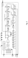
- FIG. 1 shows a block diagram of a digital frequency synthesizer IC
- FIGS. 3 A- 3 C show a conceptual flowcharts of a frequency synthesizer algorithm
- FIG. 4 shows a high-level block diagram of an adaptive variable ring-oscillator
- FIG. 5 shows a detailed schematic diagram of an adaptive DL-based ring-oscillator
- FIG. 6 shows a block diagram of a 3-bit Frac-N dithering module
- FIG. 7 shows a timing sequence of the system for different dither rates
- FIG. 8 A shows a schematic diagram of the DL-based one-shot timer for the startup procedure
- FIG. 8 B shows ring-oscillator waveforms at start-up
- FIG. 9 A shows a Layout of the frequency synthesizer IC
- FIG. 9 B shows post-layout results—frequency resolution at the ISM frequency of 6.78 MHz.
- the present invention proposes a high-performance adaptive digital frequency synthesizer integrated circuit (IC) for wireless power systems (for WPT systems), which is wide-range, high-frequency, high-resolution and scalable.
- the frequency synthesizer is a key building block of WPT controllers, which compensates on-the-fly for variations in wireless power applications.
- the new proposed synthesizer IC relies on continuous tuning of the operating frequency to the target frequency, regardless of system variations and components drifts.
- the new proposed synthesizer design allows obtaining very high accuracy and frequency resolution, while saving silicon area and power consumption.
- FIG. 1 is a block diagram of the proposed high-resolution synthesizer IC.
- the synthesizer 100 comprises a tuner unit 101 , a Serial Peripheral Interface (SPI) 102 that is pre-programmed with a set of default values for the main parameters of the synthesizer such as:
- SPI Serial Peripheral Interface
- the frequency synthesizer 101 is based on an adaptive digitally controlled tunable ring-oscillator 103 , combined with a counter-comparator 104 .
- the output signal of the synthesizer 100 is generated based on coarse, fine and ultra-fine tuning signals provided to the ring-oscillator 103 . These tuning signals are generated by the tuner unit 101 , which receives a compensation (reference) signal, c[n], from a compensator and generates arithmetic operations which are determined by a local Arithmetic Logic Unit (ALU) as detailed later on with respect to FIG. 3 A .
- a synchronization unit 105 is responsible for simultaneously passing and locking the tuning signals (received from tuner unit 101 ) every switching cycle, so as to avoid frequency glitches and false frequency tuning.
- the synchronization unit 105 outputs (locked) tuning signals Y 1 , Y 2 , Y 3 and Y 4 , which represent the coarse-tuning, fine-tuning, ultra-fine tuning and an enhancement signal, respectively.
- These tuning signals are essential to obtain accurate, stable, wide range, high-frequency operation while maintaining a single delay-cell resolution, without significant penalty on the power consumption and silicon area, as will be described later on.
- the value of the coarse-tuning signal Y 1 defines how many ring-oscillator cycles are needed for generating the output period T sw by a counter-based signal generator 106 .
- the value of the fine-tuning signal (Y 2 ) controls the delay ring size, i.e., how many extra delay elements should be added to the basic ring-oscillator string to improve the resolution.
- the value of the ultra-fine value (Y 3 ) defines how many ring cycles should have an additional delay element within the output period.
- the enhancement signal (Y 4 ) defines when to add extra delay element to the ring-oscillator string, for further improving the resolution of the output period, effectively finer than a single cell resolution.
- the delay of a single delay stage is 1 nS and the desired resolution is 10.5 nS
- the first cycle will include the counting of 10 delay stages and the second cycle will include the counting of 11 delay stages.
- the average will be a delay of 10.5 nS.
- the desired resolution is 10.1 nS
- two cycles of the ring oscillator will be required: the counting cycles will include the counting of 10 delay stages 90 times and the last cycle will include the counting of 11 delay stages.
- the average will be a delay of 10.1 nS.
- FIG. 2 shows typical block diagram of a near-field WPT system with frequency-based controller 200 .
- primary and secondary matching networks for both the transmitter and receiver are used.
- the controller core primarily relies on several building blocks: (i) frequency synthesizer 101 , (ii) a phase detector 201 , (iii) and core control and power management module 202 to process various measurements from the system and thereby provide the necessary control signals to the DC-AC inverter.
- the phase detector 201 provides phase difference between measured voltage/current signals of the transmitter, to provide correction signal for the frequency synthesizer 101 .
- the controller provides the required PWM control signal.
- the controller 200 provides the necessary control signals to adjust the passive components.
- the controller 200 also processes information from the receiver provided via a communication interface 203 (typically Bluetooth), for allowing device/s to connect (disconnect), adjustments in control signals and other system parameters that allows proper wireless power operation.
- a communication interface 203 typically Bluetooth
- FIGS. 3 A- 3 C illustrate flowcharts of the frequency regulation procedure, describing the principle of operation of the new high-performance digital frequency synthesizer IC.
- the coarse-tuning (denoted as Y 1 ) defines how many ring-oscillator cycles are needed for generating the output period.
- the fine-tuning value (Y 2 ) controls the delay ring size, i.e., how many extra delay elements should be added to the basic ring-oscillator string to improve the resolution.
- the ultra-fine value (Y 3 ) defines how many ring cycles should have an additional delay element within the output period. Based on the ultra-fine and coarse signals, a counter-comparator unit is responsible for enabling the additional delay (as shown in FIG. 3 B ).
- a frequency dithering (dithering is the process of adding noise to a signal, in an effort to mask and randomize higher-order harmonics, and in turn, make quantization distortion less perceivable) feature [32]-[35] outputting an enhancement signal (Y 4 ) has been embedded in the frequency synthesizer.
- the enhancement signal (Y 4 ) defines and enables to add extra delay element to the ring-oscillator string, for further improving the resolution of the output period, effectively finer than a single cell resolution.
- a high-resolution output period is generated (as shown in FIG. 3 C ).
- the duty-cycle of the output signal is 50% but if required, it can be also adjusted with high-resolution tuning.
- the internal high-resolution reference clock signal f ring (Local Clock) should be greater than f sw by an order of magnitude.
- too high f ring is not desired.
- FIG. 3 A is a flowchart of the operations performed to generate the signals Y 1 , Y 2 , Y 3 , Y 4 provided by the tuner 101 and the synchronization unit 105 .
- an initial period value, the duty cycle, the value of the compensation (reference) signal and the control gain are input to the tuner 101 .
- P i is the initial period value
- g c is the compensation gain
- P c is the compensation value
- L 0 is the base ring oscillator length
- L 0 is the base ring oscillator length
- FIG. 3 B is a flowchart of the operations performed to generate the modulo signal provided by the counter-comparator unit 104 .
- the values Y 1 and Y 3 are input to the counter-comparator unit 104 and the count value is set to 0.
- the counter-comparator unit 104 waits to receive the local clock signal of the ring oscillator 103 .
- the process checks if count ⁇ Y 3 . If yes, at the next step 310 the modulo value is set to “1” and counting is advanced at step 311 using the “1”. If no, at the next step 312 , the modulo value is set to “0”.
- the process checks if count ⁇ Y 1 . If no, counting is advanced at step 311 using the “0”. If yes, the modulo signal is determined.
- FIG. 3 C is a flowchart of the operations performed to generate the output frequency f sw provided by the counter-based signal generator 106 .
- the value Y 1 is input to the counter-based signal generator 106 and the count value is set to 0.
- the counter-based signal generator 106 waits to receive the local clock signal of the ring oscillator 103 .
- the process checks if count ⁇ Y 1 /2. If yes, at the next step 317 the output value is set to “1” and counting is advanced at step 318 using the “1”. If no, at the next step 319 , the output value is set to “0”.
- the process checks if count ⁇ Y 1 . If no, counting is advanced at step 318 using the “0”. If yes, output signal is determined.
- the present invention proposes the realization of both area and power efficient high-performance frequency synthesizer IC suitable for the strict demands of WPT systems in general, and in particular of resonant-based WPT systems [36], [37].
- the main enabler to achieve the latter is that the fundamental units in this invention have been implemented as an asynchronous hardware based on standard-cell delay-lines (DL) and combinatorial circuits [38], [39]. By doing so, a significant portion of complex and power-hungry hardware for timing and high-speed synchronization is eliminated.
- FIG. 4 is a block diagram of the adaptive variable ring-oscillator.
- FIG. 5 is a block diagram of the oscillator's architecture that has been developed on the basis of all-digital standard-cell approach with a single supply domain, and can therefore be designed using a generic digital flow procedure, which is very beneficial in terms of scalability and technology advancements.
- the propagation time of the entire DL string t ring can be manually calibrated by adding/removing delay elements within the ring-oscillator (by using the SPI 102 ).
- t ring is pre-defined to be in the middle of the calibration span.
- the oscillator can be calibrated to 16 different options, and is able to generate frequencies between approximately 1-to-10 MHz.
- f ring is the frequency of the ring-oscillator 103 (denoted as ‘Local Clock’ at FIG. 1 and represents an internal high-resolution reference clock signal)
- t DE is the delay of a single delay-element within the ring-oscillator
- N is adjustable overall number of the delay elements in the ring
- CNT per is an integer represents the coarse value of the counter for generating the target output frequency f sw (period-T sw ). From Formula (1), it can be observed that f sw can be varied by adjusting t ring and CNT per .
- t ring is primarily determined by the main DL string (as shown at FIG. 5 ), and can be adjusted by: (i) fine value which with the aid of the MUX determines how many extra DE (DLY 0 -DLY 7 ) would be added to the main DL string to improve the resolution; (ii) modulus bit (produced by a modulus bit block), which is determined by the ultra-fine value; (iii) dither bit (produced by a dither bit module) which enables to further improve the resolution of t ring , is determined by the enhancement value.
- the frequency resolution of the frequency synthesizer, f res can be calculated as the LSB change in CNT per :
- Some commercial microcontroller products include a frequency resolution enhancement (hardware embedded) by a variation of Frac-N method and additional features dedicated to power applications [43]-[46].
- a significant drawback of the approach implemented in these products which is based on the use of a fixed dither period for all fractional frequencies of the digitally controlled oscillator, is a considerably slow response of the system in closed-loop operation.
- FIG. 6 is a block diagram of a 3-bit Fractional-N dithering module.
- the method of its operation applies an adaptive dither rate based on the desired accuracy (an enhancement signal which is determined by the tuner unit 101 ) which improves the resolution of the ring-oscillator and hence the overall resolution of the frequency synthesizer is significantly improved.
- the implementation of the dither algorithm on digital platforms is straightforward with minimum hardware complexity.
- the adaptive Fractional-N dithering method is facilitated by dithering the oscillator between CNT per and CNT per +1 at a defined rate, varied by the required accuracy.
- the dither factor, n is the number of oscillator cycles needed to achieve the desired fractional frequency. Dithering is accomplished by keeping a constant period over (n ⁇ 1) oscillator cycles (referred as base period) and then changing the last slot (n) to another period. Then, the resolution provided by a single delay-line cell of the ring-oscillator, is averaged.
- the resultant (average) frequency in this method can be calculated by a general expression as follows:
- FIG. 7 An example for dither rates that can be generated by a 3-bit Fractional-N dithering module with respect to the Enhancement value and Local Clock signal is shown in FIG. 7 .
- the oscillator used by the present invention primarily relies on delays and counting the propagation of ‘1’ within the string. This implies that for ramping-up the oscillator (and the frequency synthesizer) and stimulating the system, high logic level needs to propagate within the DL string at initialization.
- a DL-based one-shot timer has been realized, as shown at FIG. 8 A .
- the enable signal, EN is provided to the IC, at initialization the flip-flop generates ‘1’ that is being passed throughout the ring-oscillator string triggering the system (by a triggering signal), and therefore, an initial f ring is generated.
- the oscillator is an adaptive standalone unit that depends on the value of MUX out signal, the one-shot timer generates a short pulse that is determined by the propagation time of QB. Therefore, after initialization only MUX out is responsible for triggering the oscillator every cycle.
- FIG. 8 B An Illustrative example that depicts the waveforms of the oscillator at start-up procedure is shown at FIG. 8 B .
- a high-performance frequency synthesizer IC has been designed and implemented in 0.18- ⁇ m, where the effective die area of the synthesizer is 0.1 mm 2 , the chip layout is shown at FIG. 9 A .
- Post-layout analysis shows that at ISM frequency of 6.78 MHz, the effective frequency resolution is approximately ⁇ 1.25 kHz, which satisfies the allocated frequency bandwidth according to alliance for wireless power consortium [47].
Landscapes
- Physics & Mathematics (AREA)
- Nonlinear Science (AREA)
- Stabilization Of Oscillater, Synchronisation, Frequency Synthesizers (AREA)
- Transceivers (AREA)
Abstract
Description
-
- a. a digitally controlled tunable ring-oscillator, based on a chain of delay-line cells (DLs) being adapted to generate an internal high-resolution reference clock signal fring;
- b. a tuner unit for receiving as input a compensation/target signal and performing arithmetic operations that produce auxiliary tuning signals provided to the ring-oscillator, for allowing the ring-oscillator to generate a high-resolution output period/frequency;
- c. a counter-comparator unit introducing an additional delay to the chain, the counter-comparator unit operating in combination with the ring-oscillator and counts how many times the delay of the chain repeats, for providing ultra-fine tuning signal for tuning the frequency resolution of digitally controlled ring-oscillator; and
- d. an adaptive Fractional-N dithering module, for enhancing the frequency resolution of the digitally controlled ring-oscillator by averaging the resolution provided by a single delay-line cell of the ring-oscillator.
-
- a. a coarse-tuning signal (Y1) that defines how many complete oscillator cycles are needed for generating the output period/frequency;
- b. a fine-tuning signal (Y2) that defines how many extra delay elements should be added to the oscillator's chain to improve the resolution;
- c. an ultra-fine-tuning signal (Y3) that defines how many oscillator cycles should have an additional delay element within the output period; and
- d. an enhancement signal (Y4) that defines the sequencing of adding an extra delay element to the oscillator chain, for further improving the resolution of the output period to be finer than the resolution of a single delay-line cell.
-
- a. the coarse tuning signal;
- b. the ultra-fine tuning signal; and
- c. the internal reference clock fring,
and outputs a modulus signal which allows adding an extra delay-line cell to the ring-oscillator, to improve the resolution of the output signal.
-
- receive the enhancement signal and the internal reference clock signal fring provided by the ring-oscillator;
- perform a logic operation between the enhancement signal and the internal reference clock signal fring;
- produce a Dither signal which sequentially enables adding extra delay-element to the ring-oscillator, to further improve the resolution of the output signal.
-
- a. a start-up circuit, which receives as input an enable signal and outputs a triggering signal to initiate a tuning procedure upon power-up of the frequency synthesizer, and to synthesize the internal reference clock fring;
- b. a calibration module, which receives calibration signals from a serial communications port, and compensates for variations in process, voltage and temperature, and for post-fabrication mismatches;
- c. a Modulus bit block which receives as input the Modulus signal and a delayed version of the internal reference clock fring and increases or decreases the delay within the ring-oscillator;
- d. a Dither bit module for increasing/decreasing sequenced delay within the oscillator, which receives as input the Dither signal and a delayed version of the internal reference clock fring; and
- e. main DL-string and fine-tuning DL-string for producing high-resolution feedback signal to fine-tune the internal reference clock fring, which receives as input:
- i. the Dither signal; and
- ii. delayed version of the internal reference clock fring;
-
- a. generating an internal high-resolution reference clock signal fring by digitally controlled tunable ring-oscillator, based on a chain of delay-line cells (DLs);
- b. receiving by a tuner unit, a compensation/target signal and performing arithmetic operations that produce auxiliary unit signals provided to the ring-oscillator, for allowing the ring-oscillator to generate a high-resolution output period/frequency;
- c. providing, by a counter-comparator unit, ultra-fine tuning signal for tuning the frequency resolution of digitally controlled ring-oscillator; and
- d. enhancing, by an adaptive Fractional-N dithering module, the frequency resolution of the digitally controlled ring-oscillator by averaging the resolution provided by a single cell of the ring-oscillator.
-
- the initial period value;
- the reference value;
- the (variable) duty-cycle;
- the gain,
- which determine the target output period Tsw and the derived output frequency fsw.
P=floor(P/L 0);
R=modulo(P/L 0);
Y 2=floor[(R/Y 1)−L 0);
Y 3=modulo(R/Y 1).
Y 4=round[N D(P i +g c P c −P)];
R=modulo(P/L 0);
-
- a. Given target frequency of fsw=6.785 MHz, which translated to time period of Tsw=147.384 ns.
- b. Given that the propagation time of a single delay element is tDE=200 ps; (Pi+gcPc) can be found by the ratio between Tsw and tD as follows:
P i +g c P c =T sw /t DE=736.920 - c. According to stage I (
FIG. 3A ), P=736. - d. Given that the base ring-oscillator length is L0=64, according to stage II (
FIG. 3A ) the coarse value Y1=11, with residue of R=32. - e. According to stage III (
FIG. 3A ) the fine value Y2=2, and the ultra-fine value Y3=10. - f. Given that the number of dither segments is ND=8, according to stage IV (
FIG. 3A ) the enhancement value Y4=7. - g. Having the auxiliary tuning signals Y1-Y4, the operations in
FIGS. 3B and 3C can be activated; thus, a high-resolution output signal can be generated.
-
- and the enhanced frequency resolution:
-
- [1] T. Imura and Y. Hori, “Maximizing air gap and efficiency of magnetic resonant coupling for wireless power transfer using equivalent circuit and Neumann formula,” IEEE Trans. Ind. Electron, vol. 58, no. 10, pp. 4746-4752, October 2011.
- [2] T. Langlotz, T. Nguyen, D. Schmalstieg, and R. Grasset, “Next generation augmented reality browsers: Rich, seamless, and adaptive,” in Proc. IEEE, vol. 102, no. 2, pp. 155-169, February 2014.
- [3] D. Xu, L. Han, M. Tan, and Y. F. Li, “Ceiling-based visual positioning for an indoor mobile robot with monocular vision,” IEEE Trans. Ind. Electron, vol. 56, no. 5, pp. 1617-1628, May 2009.
- [4] S. Li and C. Mi, “Wireless Power Transfer for Electric Vehicle Applications,” IEEE Journal of Emerging and Selected Topics in Power Electronics, vol. PP, pp. 1-1, 2014.
- [5] S. Jaegue et al., “Design and implementation of shaped magnetic resonance-based wireless power transfer system for roadway-powered moving electric vehicles,” IEEE Trans. Ind. Electron, vol. 61, no. 3, pp. 1179-1192, March 2014.
- [6] L. Collins, “Cut the cord,” Electron. Syst. Softw, vol. 5, no. 6, pp. 42-46, January-December 2007.
- [7] F. Musavi and W. Eberle, “Overview of wireless power transfer technologies for electric vehicle battery charging,” IET Power Electronics, vol. 7, no. 1, pp. 60-66, 2014.
- [8] D. C. Bock, A. C. Marschilok, K. J. Takeuchi, and E. S. Takeuchi, “Batteries used to power implantable biomedical devices,” Electrochimica Acta, vol. 84, pp. 155-164, 2012.
- [9] F. Lu, H. Zhang, C. Mi, “A two-plate capacitive wireless power transfer system for electric vehicle charging Applications,” IEEE Trans. Power Electron, vol. 33, no. 2, pp. 946-969, August 2017.
- [10] F. Lu, H. Zhang, H. Hofmann, and C. Mi, “A double-sided LC compensation circuit for loosely-coupled capacitive power transfer,” IEEE Trans. Power Electron, vol. 33, no. 2, pp. 1633-1643, February 2017.
- [11] J. Dai and D. C Ludois, “A survey of wireless power transfer and a critical comparison of inductive and capacitive coupling for small gap applications,” IEEE Trans. Power Electron, vol. 30, no. 11, pp. 6017-6029, November 2015.
- [12] F. Lu, H. Zhang, H. Hofmann, and C. Mi, “A double-sided LCLC compensated capacitive power transfer system for electric vehicle charging,” IEEE Trans. Power Electron, vol. 30, no. 11, pp. 6011-6014, June 2015.
- [13] H. Zhang, F. Lu, H. Hofmann, W. Liu, and C. C. Mi, “A four-plate compact capacitive coupler design and LCL-compensated topology for capacitive power transfer in electric vehicle charging application,” IEEE Trans. Power Electron, vol. 31, no. 12, pp. 8541-8551, December 2016.
- [14] F. Lu, H. Zhang, H. Hofmann, C. Mi, “A loosely coupled capacitive power transfer system with LC compensation circuit topology,” Proc. IEEE Energy Conyers. Congr. Expo. (ECCE), pp. 1-5, 2016.
- [15] F. Lu, H. Zhang, H. Hofmann, and C. Mi, “A double-sided LC compensation circuit for loosely-coupled capacitive power transfer,” IEEE Trans. Power Electron, vol. 33, no. 2, pp. 1633-1643, February 2017.
- [16] H. Li, J. Li, K. Wang, W. Chen, and Y. Xu, “A maximum efficiency point tracking control scheme for wireless power transfer systems using magnetic resonant coupling,” IEEE Trans. Power Electron, vol. 30, no. 7, pp. 3998-4008, July 2015.
- [17] T. D. Yeo, D. Kwon, S. T. Khang, and J. W. Yu, “Design of maximum efficiency tracking control scheme for closed-loop wireless power charging system employing series resonant tank,” IEEE Trans. Power Electron, vol. 32, no. 1, pp. 471-478, January 2017.
- [18] N. Y. Kim, K. Y. Kim, J. Choi, and C. W. Kim, “Adaptive frequency with power-level tracking system for efficient magnetic resonance wireless power transfer,” Electron. Lett, vol. 48, no. 8, pp. 452-454, April 2012.
- [19] N. Y. Kim et al., “Automated adaptive frequency tracking system for efficient mid-range wireless power transfer via magnetic resonant coupling,” in Proc. 42nd Eur. Microw. Conf., 2012, pp. 221-224.
- [20] K. Lu, S. K. Nguang, S. Ji, and L. Wei, “Design of auto frequency tuning capacitive power transfer system based on class-E2 dc/dc converter,”IET Power Electronics, vol. 10, no. 12, pp. 1588-1595, 2017.
- [21] M. Kline, I. Izyumin, B. Boser, and S. Sanders, “Capacitive power transfer for contactless charging,” in Proc. IEEE Appl. Power Electron. Conf. Expo., 2011, pp. 1398-1404.
- [22] P. Si, A. P. Hu, S. Malpas, and D. Budgett, “A frequency control method for regulating wireless power to implantable devices,” IEEE Trans. Biomed. Circuits Syst, vol. 2, no. 1, pp. 22-29, March 2008.
- [23] Y. Jiang et al. “Analysis, Design and implementation of WPT system for EV's battery charging based on optimal operation frequency range,” in IEEE Transactions on Power Electronics, vol. 34, no. 7, pp. 6890-6905, July 2018.
- [24] Y. Jiang, Y. Wang, J. Liu, X. Li, and L. Wang, “An accurate phase detection method for realizing ZVS of high frequency inverter in wireless power transmission,” in Proc. Future Energy Electron. Conf. ECCE Asia, 2017, pp. 1380-1384.
- [25] H. G. Park et al., “A design of a wireless power receiving unit with a high-efficiency 6.78-MHz active rectifier using shared DLLs for magnetic-resonant A4 WP applications,” IEEE Trans. Power Electron, vol. 31, no. 6, pp. 4484-4498, June 2016.
- [26] E. Abramov, T. Vekslender, O. Kirshenboim, and M. M. Peretz, “Fully-integrated digital average current-mode control voltage regulator module IC,” IEEE Journal on Emerging and Selected Topics in Power Electronics, vol. 6, no. 2, pp. 549-562, June 2018.
- [27] M. Rodriguez, Y. Zhang, and D. Maksimovic, “High-frequency PWM buck converters using GaN-on-SiC HEMTs,” IEEE Trans. Power Electron, vol. 29, no. 5, pp. 2462-2473, May 2014.
- [28] Y. Zhang, M. Rodriguez, and D. Maksimovic, “Very high frequency PWM buck converters using monolithic GaN half-bridge power stages with integrated gate drivers,” IEEE Trans. Power Electron, vol. 31, no. 11, pp. 7926-7942, November 2016.
- [29] Altera (2012, September) Transciever Overview: Stratix IV and Hard-Copy IV. [Online]. Avialable: http://www.altera.com/devices/fpga/stratixfpgas/stratix-iv/transceivers/stxiv-transceivers.html
- [30] B. H. Waters, A. P. Sample, J. R. Smith, “Adaptive impedance matching for magnetically coupled resonators,” in Proc. Prog. Electromagn. Res. Symp., 2012, pp. 694-701.
- [31] F. C. Commission, “Cfr 18-industrial, scientific and medical equipment,” Code Federal Regulations, pp. 862-868, 2008.
- [32] M. M. Peretz and S. Ben-Yaakov, “Digital control of resonant converters: enhancing frequency resolution by dithering,” in Proc. IEEE Applied Power Electronics Conference and Exposition (APEC), February 2009, pp. 1202-1207.
- [33] M. Hovin, A. Olsen, T. S. Lande, and C. Toumazou, “Delta-sigma modulators using frequency-modulated intermediate values”, IEEE Journal of Solid-State Circuits, vol. 32, no. 1, pp. 13-22, January 1997.
- [34] A. V. Peterchev and S. R. Sanders, “Quantization resolution and limit cycling in digitally controlled PWM converters,” IEEE Trans. Power Electron, vol. 18, no. 1, pp. 301-308, January 2003.
- [35] Z. Lukic, N. Rahman, and A. Prodic, “Multi-bit S-D PWM digital controller IC for DC-DC converters operating at switching frequencies beyond 10 MHz,” IEEE Trans. Power Electron, vol. 22, no. 5, pp. 1693-1707, September 2012.
- [36] Z. Pantic and S. M. Lukic, “Framework and topology for active tuning of parallel compensated receivers in power transfer systems,” IEEE Trans. Power Electron, vol. 27, no. 11, pp. 4503-4513, November 2012.
- [37] B. L. Cannon, J. F. Hoburg, D. D. Stancil, and S. C. Goldstein, “Magnetic resonant coupling as a potential means for wireless power transfer to multiple small receivers,” IEEE Trans. Power Electron, vol. 24, no. 7, pp. 1819-1825, July 2009.
- [38] B. J. Patella, A. Prodić, A. Zirger, and D. Maksimović, “High-frequency digital PWM controller IC for DC-DC converters,” IEEE Trans. Power Electron, vol. 18, no. 1, pp. 438-446, January 2003.
- [39] O. Trescases, A. Prodić, Wai Tung Ng, “Digitally controlled current-Mode DC-DC converter IC,” IEEE Trans. Circuits Syst. I, Reg. Papers, vol. 58, no. 1, pp. 219-231, January 2011.
- [40] A. Abidi, “Phase noise and jitter in CMOS ring oscillators,” IEEE J. Solid-State Circuits, vol. 41, no. 8, pp. 1803-1816, August 2006.
- [41] Pepe, Federico and Pietro Andreani. “An accurate analysis of phase noise in CMOS ring oscillators.” IEEE Transactions on Circuits and Systems II: Express Brief, vol. 66, no. 8, pp. 1292-1296, December 2018.
- [42] W. Bae, H. Ju, K. Park, S-Y. Cho, and D-K. Jeong, “A 7.6 mW, 414 fs RMS-jitter 10 GHz phase-locked loop for a 40 Gb/s serial link transmitter based on a two-stage ring oscillator in 65 nm CMOS,’ IEEE J. Solid-State Circuits, vol. 51, no. 10, pp. 2357-2367, October 2016.
- [43] Atmel Corporation, “AT90PWMx microcontrollers data sheet”, available at www.atmel.com, Doc No. doc7710.pdf.
- [44] Microchip Technology, “dsPIC30F SMPS reference manual, sec. 29 oscillator section”, available at www.microchip.com, Doc No. 70268A.pdf.
- [45] STMicroelectronics, “PWM resolution enhancement through a dithering technique for STM32 advanced-configuration, general-purpose and lite timers”, available at www.st.com, Doc No. en.DM00119042.pdf.
- [46] Texas Instrument, “AN-1879 Fractional N Frequency Synthesis”, available at http://www.ti.com, Doc No. en.DM00119042.pdf.
- [47] R. Tseng, B. von Novak, S. Shevde, and K. A. Grajski, “Introduction to the Alliance for Wireless Power Loosely-Coupled Wireless Power Transfer System Specification Version 1.0,” IEEE Wireless Power Transfer Conference, Perugia, Italy, May 2013.
Claims (15)
Applications Claiming Priority (3)
| Application Number | Priority Date | Filing Date | Title |
|---|---|---|---|
| IL275511A IL275511B2 (en) | 2020-06-18 | 2020-06-18 | High-accuracy adaptive digital frequency synthesizer for wireless power systems |
| IL275511 | 2020-06-18 | ||
| PCT/IL2021/050737 WO2021255739A1 (en) | 2020-06-18 | 2021-06-17 | High-accuracy adaptive digital frequency synthesizer for wireless power systems |
Publications (2)
| Publication Number | Publication Date |
|---|---|
| US20230253959A1 US20230253959A1 (en) | 2023-08-10 |
| US12047077B2 true US12047077B2 (en) | 2024-07-23 |
Family
ID=79268591
Family Applications (1)
| Application Number | Title | Priority Date | Filing Date |
|---|---|---|---|
| US18/010,234 Active US12047077B2 (en) | 2020-06-18 | 2021-06-17 | High-accuracy adaptive digital frequency synthesizer for wireless power systems |
Country Status (5)
| Country | Link |
|---|---|
| US (1) | US12047077B2 (en) |
| EP (1) | EP4169163A4 (en) |
| CN (1) | CN115917973A (en) |
| IL (1) | IL275511B2 (en) |
| WO (1) | WO2021255739A1 (en) |
Cited By (1)
| Publication number | Priority date | Publication date | Assignee | Title |
|---|---|---|---|---|
| US20250167591A1 (en) * | 2022-06-15 | 2025-05-22 | Capow Technologies Ltd | Wide-range power-regulation method for wireless power receiving units by using hybrid multi-level topologies |
Citations (9)
| Publication number | Priority date | Publication date | Assignee | Title |
|---|---|---|---|---|
| US20100260242A1 (en) | 2008-03-04 | 2010-10-14 | Katsuaki Abe | Time digital converter, digital pll frequency synthesizer, transceiver, and receiver |
| US20160006421A1 (en) | 2014-07-04 | 2016-01-07 | Nxp B.V. | Frequency synthesiser circuit |
| US20160118990A1 (en) | 2013-05-31 | 2016-04-28 | The Regents Of The University Of Michigan | Automatically placed-and-routed adpll with pwm-based dco resolution enhancement |
| US20160359493A1 (en) | 2015-06-01 | 2016-12-08 | University Of Southern California | Adaptive spur cancellation techniques and multi-phase injection locked tdc for digital phase locked loop circuit |
| US20170012632A1 (en) | 2015-07-08 | 2017-01-12 | Denso Corporation | Digital Control Oscillator Circuit |
| US20170244544A1 (en) | 2016-02-24 | 2017-08-24 | The Regents Of The University Of California | Digital fractional-n pll based upon ring oscillator delta-sigma frequency conversion |
| CN110838845A (en) | 2019-11-19 | 2020-02-25 | 中山大学 | TDC based on multiphase ring oscillator and annular pulse contraction delay chain |
| US10790837B1 (en) * | 2019-10-22 | 2020-09-29 | Qualcomm Incorporated | Self-tuning digital clock generator |
| US10826501B1 (en) * | 2019-06-24 | 2020-11-03 | Silicon Laboratories Inc. | Ring oscillator based RC calibration circuit |
Family Cites Families (2)
| Publication number | Priority date | Publication date | Assignee | Title |
|---|---|---|---|---|
| US5799049A (en) * | 1996-04-02 | 1998-08-25 | Motorola, Inc. | Phase-independent clock circuit and method |
| JP3540589B2 (en) * | 1998-02-02 | 2004-07-07 | 株式会社東芝 | Clock multiplication circuit |
-
2020
- 2020-06-18 IL IL275511A patent/IL275511B2/en unknown
-
2021
- 2021-06-17 WO PCT/IL2021/050737 patent/WO2021255739A1/en not_active Ceased
- 2021-06-17 US US18/010,234 patent/US12047077B2/en active Active
- 2021-06-17 CN CN202180043282.1A patent/CN115917973A/en active Pending
- 2021-06-17 EP EP21825436.5A patent/EP4169163A4/en active Pending
Patent Citations (9)
| Publication number | Priority date | Publication date | Assignee | Title |
|---|---|---|---|---|
| US20100260242A1 (en) | 2008-03-04 | 2010-10-14 | Katsuaki Abe | Time digital converter, digital pll frequency synthesizer, transceiver, and receiver |
| US20160118990A1 (en) | 2013-05-31 | 2016-04-28 | The Regents Of The University Of Michigan | Automatically placed-and-routed adpll with pwm-based dco resolution enhancement |
| US20160006421A1 (en) | 2014-07-04 | 2016-01-07 | Nxp B.V. | Frequency synthesiser circuit |
| US20160359493A1 (en) | 2015-06-01 | 2016-12-08 | University Of Southern California | Adaptive spur cancellation techniques and multi-phase injection locked tdc for digital phase locked loop circuit |
| US20170012632A1 (en) | 2015-07-08 | 2017-01-12 | Denso Corporation | Digital Control Oscillator Circuit |
| US20170244544A1 (en) | 2016-02-24 | 2017-08-24 | The Regents Of The University Of California | Digital fractional-n pll based upon ring oscillator delta-sigma frequency conversion |
| US10826501B1 (en) * | 2019-06-24 | 2020-11-03 | Silicon Laboratories Inc. | Ring oscillator based RC calibration circuit |
| US10790837B1 (en) * | 2019-10-22 | 2020-09-29 | Qualcomm Incorporated | Self-tuning digital clock generator |
| CN110838845A (en) | 2019-11-19 | 2020-02-25 | 中山大学 | TDC based on multiphase ring oscillator and annular pulse contraction delay chain |
Non-Patent Citations (1)
| Title |
|---|
| Search Report and Written Opinion issued in PCT Application No. PCT/IL2021/050737, mailed Oct. 20, 2021. |
Cited By (2)
| Publication number | Priority date | Publication date | Assignee | Title |
|---|---|---|---|---|
| US20250167591A1 (en) * | 2022-06-15 | 2025-05-22 | Capow Technologies Ltd | Wide-range power-regulation method for wireless power receiving units by using hybrid multi-level topologies |
| US12489315B2 (en) * | 2022-06-15 | 2025-12-02 | Capow Technologies Ltd | Wide-range power-regulation method for wireless power receiving units by using hybrid multi-level topologies |
Also Published As
| Publication number | Publication date |
|---|---|
| EP4169163A1 (en) | 2023-04-26 |
| WO2021255739A1 (en) | 2021-12-23 |
| CN115917973A (en) | 2023-04-04 |
| IL275511A (en) | 2022-01-01 |
| IL275511B2 (en) | 2023-11-01 |
| US20230253959A1 (en) | 2023-08-10 |
| IL275511B1 (en) | 2023-07-01 |
| EP4169163A4 (en) | 2024-08-28 |
Similar Documents
| Publication | Publication Date | Title |
|---|---|---|
| US10008980B2 (en) | Wideband digitally controlled injection-locked oscillator | |
| US10965156B2 (en) | Capacitive wireless power transfer by means of adaptive matching networks | |
| EP2451081A1 (en) | Pll circuit, and radio communication device equipped therewith | |
| Abramov et al. | Adaptive self-tuned controller IC for resonant-based wireless power transfer transmitters | |
| US12047077B2 (en) | High-accuracy adaptive digital frequency synthesizer for wireless power systems | |
| US20100007390A1 (en) | Clock generating circuit, power converting system, and related method with spread spectrum for EMI reduction | |
| Wang et al. | A digital to time converter with fully digital calibration scheme for ultra-low power ADPLL in 40 nm CMOS | |
| CN101741250B (en) | Pulse Width Modulation Control Circuit and Method for Reducing Electromagnetic Interference by Mains Frequency Modulation | |
| EP2329597B1 (en) | Oscillating circuit, dc-dc converter, and semiconductor device | |
| US9806701B1 (en) | Digital frequency multiplier to generate a local oscillator signal in FDSOI technology | |
| Rehman et al. | An ultra-low-power 2.4 GHz all-digital phase-locked loop with injection-locked frequency multiplier and continuous frequency tracking | |
| Abramov et al. | Adaptive self-tuned mixed-signal controller IC for resonant wireless power transfer | |
| CN103916124A (en) | Injection locking frequency division structure with automatic frequency verification function | |
| WO2006039187A3 (en) | Sigma-delta based phase lock loop | |
| WO2016155278A1 (en) | Circuit and equipment for quickly locking microwave frequency source | |
| US7277519B2 (en) | Frequency and phase correction in a phase-locked loop (PLL) | |
| TW200525895A (en) | Auto loop gain calibration of a synthesizer | |
| Wang et al. | A Time and Energy-Efficient Asynchronous Hybrid-Searching Auto Frequency Calibration for a 3.2 GHz Phase-Locked Loop | |
| US20100176888A1 (en) | Voltage-controlled oscillator, frequency synthesizer, and oscillation frequency control method | |
| CN118316443B (en) | Low-phase-noise fractional frequency-division phase-locked loop, chip and electronic equipment | |
| Abramov et al. | Regulated power transfer using self-tuned networks for capacitive wireless systems | |
| TWI527380B (en) | Frequency locking device | |
| US20090322433A1 (en) | Method of Controlling Voltage-Controlled Oscillator | |
| Kim et al. | Low power FSK transmitter using all-digital PLL for IEEE 802.15. 4g application | |
| Verma et al. | COMPARATIVE STUDY OF CMOS FRACTIONAL-N SYNTHESIZER BASED ON PHASE LOCKED LOOP-A REVIEW |
Legal Events
| Date | Code | Title | Description |
|---|---|---|---|
| AS | Assignment |
Owner name: CAPOW TECHNOLOGIES LTD, ISRAEL Free format text: ASSIGNMENT OF ASSIGNORS INTEREST;ASSIGNOR:CERVERA, ALON;REEL/FRAME:062083/0555 Effective date: 20210803 |
|
| FEPP | Fee payment procedure |
Free format text: ENTITY STATUS SET TO UNDISCOUNTED (ORIGINAL EVENT CODE: BIG.); ENTITY STATUS OF PATENT OWNER: SMALL ENTITY |
|
| FEPP | Fee payment procedure |
Free format text: ENTITY STATUS SET TO SMALL (ORIGINAL EVENT CODE: SMAL); ENTITY STATUS OF PATENT OWNER: SMALL ENTITY |
|
| STPP | Information on status: patent application and granting procedure in general |
Free format text: DOCKETED NEW CASE - READY FOR EXAMINATION |
|
| STPP | Information on status: patent application and granting procedure in general |
Free format text: NON FINAL ACTION MAILED |
|
| STPP | Information on status: patent application and granting procedure in general |
Free format text: RESPONSE TO NON-FINAL OFFICE ACTION ENTERED AND FORWARDED TO EXAMINER |
|
| STPP | Information on status: patent application and granting procedure in general |
Free format text: NOTICE OF ALLOWANCE MAILED -- APPLICATION RECEIVED IN OFFICE OF PUBLICATIONS |
|
| ZAAB | Notice of allowance mailed |
Free format text: ORIGINAL CODE: MN/=. |
|
| STPP | Information on status: patent application and granting procedure in general |
Free format text: AWAITING TC RESP., ISSUE FEE NOT PAID |
|
| STPP | Information on status: patent application and granting procedure in general |
Free format text: NOTICE OF ALLOWANCE MAILED -- APPLICATION RECEIVED IN OFFICE OF PUBLICATIONS |
|
| STPP | Information on status: patent application and granting procedure in general |
Free format text: PUBLICATIONS -- ISSUE FEE PAYMENT VERIFIED |
|
| STCF | Information on status: patent grant |
Free format text: PATENTED CASE |