US12041808B2 - Electroluminescent display substrate, manufacturing method thereof, and electroluminescent display device - Google Patents
Electroluminescent display substrate, manufacturing method thereof, and electroluminescent display device Download PDFInfo
- Publication number
- US12041808B2 US12041808B2 US17/255,107 US202017255107A US12041808B2 US 12041808 B2 US12041808 B2 US 12041808B2 US 202017255107 A US202017255107 A US 202017255107A US 12041808 B2 US12041808 B2 US 12041808B2
- Authority
- US
- United States
- Prior art keywords
- layer
- base substrate
- post spacer
- overcoat
- orthographic projection
- Prior art date
- Legal status (The legal status is an assumption and is not a legal conclusion. Google has not performed a legal analysis and makes no representation as to the accuracy of the status listed.)
- Active, expires
Links
- 239000000758 substrate Substances 0.000 title claims abstract description 223
- 238000004519 manufacturing process Methods 0.000 title claims description 18
- 125000006850 spacer group Chemical group 0.000 claims abstract description 181
- 239000010409 thin film Substances 0.000 claims abstract description 51
- 229910010272 inorganic material Inorganic materials 0.000 claims abstract description 45
- 239000011147 inorganic material Substances 0.000 claims abstract description 45
- 230000000149 penetrating effect Effects 0.000 claims abstract description 7
- XLYOFNOQVPJJNP-UHFFFAOYSA-N water Substances O XLYOFNOQVPJJNP-UHFFFAOYSA-N 0.000 claims description 74
- 230000000903 blocking effect Effects 0.000 claims description 67
- 238000000034 method Methods 0.000 claims description 35
- 239000010408 film Substances 0.000 claims description 31
- 238000002161 passivation Methods 0.000 claims description 30
- 238000000059 patterning Methods 0.000 claims description 23
- 239000000463 material Substances 0.000 claims description 21
- 239000011368 organic material Substances 0.000 claims description 9
- 229920002120 photoresistant polymer Polymers 0.000 claims description 8
- 239000010410 layer Substances 0.000 description 410
- QVGXLLKOCUKJST-UHFFFAOYSA-N atomic oxygen Chemical compound [O] QVGXLLKOCUKJST-UHFFFAOYSA-N 0.000 description 18
- 229910052760 oxygen Inorganic materials 0.000 description 18
- 239000001301 oxygen Substances 0.000 description 18
- 239000011229 interlayer Substances 0.000 description 7
- 230000008020 evaporation Effects 0.000 description 5
- 238000001704 evaporation Methods 0.000 description 5
- 239000002346 layers by function Substances 0.000 description 5
- 230000009286 beneficial effect Effects 0.000 description 4
- 238000002347 injection Methods 0.000 description 4
- 239000007924 injection Substances 0.000 description 4
- 239000004020 conductor Substances 0.000 description 3
- 238000005520 cutting process Methods 0.000 description 3
- 238000005538 encapsulation Methods 0.000 description 3
- VYPSYNLAJGMNEJ-UHFFFAOYSA-N Silicium dioxide Chemical compound O=[Si]=O VYPSYNLAJGMNEJ-UHFFFAOYSA-N 0.000 description 2
- 230000007423 decrease Effects 0.000 description 2
- 230000000694 effects Effects 0.000 description 2
- 238000005516 engineering process Methods 0.000 description 2
- 230000005525 hole transport Effects 0.000 description 2
- 238000009434 installation Methods 0.000 description 2
- 239000012044 organic layer Substances 0.000 description 2
- 238000000206 photolithography Methods 0.000 description 2
- 239000002356 single layer Substances 0.000 description 2
- 239000000243 solution Substances 0.000 description 2
- 229910052581 Si3N4 Inorganic materials 0.000 description 1
- 239000011248 coating agent Substances 0.000 description 1
- 238000000576 coating method Methods 0.000 description 1
- 229910003460 diamond Inorganic materials 0.000 description 1
- 239000010432 diamond Substances 0.000 description 1
- 238000005530 etching Methods 0.000 description 1
- 238000007641 inkjet printing Methods 0.000 description 1
- 239000002184 metal Substances 0.000 description 1
- 238000004080 punching Methods 0.000 description 1
- HQVNEWCFYHHQES-UHFFFAOYSA-N silicon nitride Chemical compound N12[Si]34N5[Si]62N3[Si]51N64 HQVNEWCFYHHQES-UHFFFAOYSA-N 0.000 description 1
- 229910052814 silicon oxide Inorganic materials 0.000 description 1
- 239000004984 smart glass Substances 0.000 description 1
Images


Classifications
-
- H—ELECTRICITY
- H10—SEMICONDUCTOR DEVICES; ELECTRIC SOLID-STATE DEVICES NOT OTHERWISE PROVIDED FOR
- H10K—ORGANIC ELECTRIC SOLID-STATE DEVICES
- H10K59/00—Integrated devices, or assemblies of multiple devices, comprising at least one organic light-emitting element covered by group H10K50/00
- H10K59/10—OLED displays
- H10K59/12—Active-matrix OLED [AMOLED] displays
- H10K59/1201—Manufacture or treatment
-
- H—ELECTRICITY
- H10—SEMICONDUCTOR DEVICES; ELECTRIC SOLID-STATE DEVICES NOT OTHERWISE PROVIDED FOR
- H10K—ORGANIC ELECTRIC SOLID-STATE DEVICES
- H10K59/00—Integrated devices, or assemblies of multiple devices, comprising at least one organic light-emitting element covered by group H10K50/00
- H10K59/80—Constructional details
- H10K59/87—Passivation; Containers; Encapsulations
- H10K59/871—Self-supporting sealing arrangements
-
- H—ELECTRICITY
- H10—SEMICONDUCTOR DEVICES; ELECTRIC SOLID-STATE DEVICES NOT OTHERWISE PROVIDED FOR
- H10K—ORGANIC ELECTRIC SOLID-STATE DEVICES
- H10K50/00—Organic light-emitting devices
- H10K50/80—Constructional details
- H10K50/84—Passivation; Containers; Encapsulations
- H10K50/842—Containers
- H10K50/8428—Vertical spacers, e.g. arranged between the sealing arrangement and the OLED
-
- H—ELECTRICITY
- H10—SEMICONDUCTOR DEVICES; ELECTRIC SOLID-STATE DEVICES NOT OTHERWISE PROVIDED FOR
- H10K—ORGANIC ELECTRIC SOLID-STATE DEVICES
- H10K50/00—Organic light-emitting devices
- H10K50/80—Constructional details
- H10K50/84—Passivation; Containers; Encapsulations
- H10K50/844—Encapsulations
-
- H—ELECTRICITY
- H10—SEMICONDUCTOR DEVICES; ELECTRIC SOLID-STATE DEVICES NOT OTHERWISE PROVIDED FOR
- H10K—ORGANIC ELECTRIC SOLID-STATE DEVICES
- H10K59/00—Integrated devices, or assemblies of multiple devices, comprising at least one organic light-emitting element covered by group H10K50/00
- H10K59/80—Constructional details
- H10K59/87—Passivation; Containers; Encapsulations
- H10K59/871—Self-supporting sealing arrangements
- H10K59/8723—Vertical spacers, e.g. arranged between the sealing arrangement and the OLED
-
- H—ELECTRICITY
- H10—SEMICONDUCTOR DEVICES; ELECTRIC SOLID-STATE DEVICES NOT OTHERWISE PROVIDED FOR
- H10K—ORGANIC ELECTRIC SOLID-STATE DEVICES
- H10K59/00—Integrated devices, or assemblies of multiple devices, comprising at least one organic light-emitting element covered by group H10K50/00
- H10K59/80—Constructional details
- H10K59/87—Passivation; Containers; Encapsulations
- H10K59/873—Encapsulations
-
- H—ELECTRICITY
- H10—SEMICONDUCTOR DEVICES; ELECTRIC SOLID-STATE DEVICES NOT OTHERWISE PROVIDED FOR
- H10K—ORGANIC ELECTRIC SOLID-STATE DEVICES
- H10K71/00—Manufacture or treatment specially adapted for the organic devices covered by this subclass
-
- H—ELECTRICITY
- H10—SEMICONDUCTOR DEVICES; ELECTRIC SOLID-STATE DEVICES NOT OTHERWISE PROVIDED FOR
- H10K—ORGANIC ELECTRIC SOLID-STATE DEVICES
- H10K59/00—Integrated devices, or assemblies of multiple devices, comprising at least one organic light-emitting element covered by group H10K50/00
- H10K59/10—OLED displays
- H10K59/12—Active-matrix OLED [AMOLED] displays
Definitions
- the present disclosure relates to the field of display technology, in particular to an electroluminescent display substrate, a manufacturing method thereof, and an electroluminescent display device.
- an electroluminescent display device such as an OLED display device usually includes an OLED device sensitive to water and oxygen.
- the water and oxygen easily enter the OLED device from a cut surface of the hole, thereby affecting the performance and service life of the OLED device. Therefore, improving the encapsulating reliability of display devices with holes is a key issue for developers who develop such display devices.
- an electroluminescent display substrate comprising: a base substrate; a thin film transistor on the base substrate; a display light-emitting element disposed on the base substrate and located on a side of the thin film transistor away from the base substrate; an inorganic material layer disposed on the base substrate and located between the thin film transistor and the display light-emitting element; an encapsulating structure disposed on the base substrate and covering the display light-emitting element; a hole, the hole at least penetrating the encapsulating structure; at least one post spacer on the base substrate, the at least one post spacer surrounding the hole; and an overcoat layer disposed on the base substrate and covering the at least one post spacer, wherein an orthographic projection of the inorganic material layer on the base substrate at least partially overlaps with an orthographic projection of the thin film transistor on the base substrate, an orthographic projection of the at least one post spacer on the base substrate falls within an orthographic projection of the overcoat layer on the base substrate, a material of the overcoat layer
- the thin film transistor comprises a source electrode and a drain electrode, and the source electrode and the drain electrode are located in a first conductive layer;
- the inorganic material layer comprises a second conductive layer,
- the display light-emitting element comprises an anode and a cathode, and the second conductive layer electrically connects the source electrode or the drain electrode to the anode or cathode of the display light-emitting element.
- the inorganic material layer comprises a passivation layer between the thin film transistor and the display light-emitting element.
- the inorganic material layer further comprises a passivation layer between the thin film transistor and the display light-emitting element; and wherein the overcoat layer comprises a first overcoat sub-layer and a second overcoat sub-layer, the first overcoat sub-layer and the second conductive layer are located in the same layer, and the second overcoat sub-layer and the passivation layer are located in the same layer.
- the overcoat layer contacts a first side surface, a second side surface and a top surface of each post spacer, the first side of the post spacer is a side of the post spacer close to the hole, the second side of the post spacer is a side of the post spacer away from the hole, and the top surface of the post spacer is a surface of the post spacer away from the base substrate.
- the electroluminescent display substrate further comprises: a first planarization layer disposed between the thin film transistor and the inorganic material layer and covering the thin film transistor; and a support layer disposed between the base substrate and the post spacer and supporting the post spacer, wherein the first planarization layer and the support layer are located in the same layer and contain the same material.
- the orthographic projection of the at least one post spacer on the base substrate falls within an orthographic projection of the support layer on the base substrate.
- an orthographic projection of the support layer on the base substrate falls within the orthographic projection of the overcoat layer on the base substrate, and the overcoat layer covers both the post spacer and the support layer.
- the encapsulating structure comprises: a first water blocking layer on a side of the display light-emitting element away from the base substrate; a second planarization layer on a side of the first water blocking layer away from the base substrate; and a second water blocking layer on a side of the second planarization layer away from the base substrate, wherein the first water blocking layer and the second water blocking layer comprise an inorganic material, and the second planarization layer comprises an organic material, and wherein an orthographic projection of each of the first water blocking layer and the second water blocking layer on the base substrate covers an orthographic projection of each of the overcoat layer, the post spacer and the support layer on the base substrate.
- an orthographic projection of one post spacer of the at least one post spacer closest to the hole on the base substrate does not overlap with an orthographic projection of the second planarization layer on the base substrate.
- a cross section of each post spacer in a direction perpendicular to the base substrate has a shape selected from an inverted trapezoid shape, an I-shape or a T-shape.
- the display light-emitting element comprises an anode, a cathode, and a light-emitting layer sandwiched between the anode and the cathode, and at least one of the light-emitting layer and the cathode is disconnected at each post spacer.
- the at least one post spacer comprises two or more post spacers, and the two or more post spacers are disposed on the same support layer.
- the at least one post spacer comprises two or more post spacers
- the support layer comprises two or more support sub-layers
- the two or more support sub-layers support the two or more post spacers, respectively, so that a corner of the overcoat layer at a junction where each support sub-layer is connected with the post spacer supported by the support sub-layer has an obtuse angle.
- each post spacer comprises a photoresist material.
- the second conductive layer and the first conductive layer comprise the same material.
- an electroluminescent display device comprising the electroluminescent display substrate according to any one of the above embodiments is provided.
- a manufacturing method of an electroluminescent display substrate comprising: forming a thin film transistor on a base substrate; forming a planarization film layer on a side of the thin film transistor away from the base substrate, and then forming a first planarization layer and a support layer through one patterning process; forming a post spacer on a side of the support layer away from the base substrate; forming an inorganic material film layer on a side of the first planarization layer and the post spacer away from the base substrate, and then forming an inorganic material layer and an overcoat layer through one patterning process; forming a display light-emitting element on a side of the inorganic material layer and the overcoat layer away from the base substrate; forming an encapsulating structure on a side of the display light-emitting element away from the base substrate; and forming a hole that at least penetrates the encapsulating structure in an area surrounded by the post spacer, wherein an orthographic projection of the inorganic
- the thin film transistor comprises a source electrode and a drain electrode, and the source electrode and the drain electrode are located in the first conductive layer;
- the inorganic material layer comprises a second conductive layer,
- the display light-emitting element comprises an anode and a cathode, and the second conductive layer electrically connects the source electrode or the drain electrode to the anode or cathode of the display light-emitting element.
- the inorganic material layer comprises a passivation layer between the thin film transistor and the display light-emitting element.
- the inorganic material layer further comprises a passivation layer between the thin film transistor and the display light-emitting element; and wherein the overcoat layer comprises a first overcoat sub-layer and a second overcoat sub-layer, the first overcoat sub-layer and the second conductive layer are located in the same layer, and the second overcoat sub-layer and the passivation layer are located in the same layer.
- FIG. 1 is a schematic cross-sectional view of an electroluminescent display device
- FIG. 2 is a schematic cross-sectional view of a structure of the display device shown in FIG. 1 after forming a hole;
- FIG. 3 is a schematic structural view of a mask used in an evaporation process for forming a film layer of a display light-emitting element
- FIG. 4 is a plan view of an electroluminescent display substrate according to exemplary embodiments of the present disclosure.
- FIG. 5 is a schematic cross-sectional view, taken along line A-A′ in FIG. 4 , of an electroluminescent display substrate according to exemplary embodiments of the present disclosure
- FIG. 6 is a partial cross-sectional view, taken along the line A-A′ in FIG. 4 , of an electroluminescent display substrate according to exemplary embodiments of the present disclosure
- FIG. 7 is a partial cross-sectional view, taken along the line A-A′ in FIG. 4 , of an electroluminescent display substrate according to other exemplary embodiments of the present disclosure
- FIG. 8 is a partial cross-sectional view, taken along the line A-A′ in FIG. 4 , of an electroluminescent display substrate according to still other exemplary embodiments of the present disclosure
- FIGS. 9 A and 9 B are schematic cross-sectional views of a post spacer of an electroluminescent display substrate according to exemplary embodiments of the present disclosure.
- FIG. 10 is a partial enlarged view of an electroluminescent display substrate according to exemplary embodiments of the present disclosure, in which a relative relationship between the encapsulating structure and the post spacer is shown;
- FIGS. 11 A and 11 B are respectively partial enlarged views of a cross-sectional view of a display substrate according to embodiments of the present disclosure, in which the shape and relative positional relationship of the support layer and the post spacer are mainly shown;
- FIG. 12 is a flowchart of a manufacturing method of an electroluminescent display substrate according to exemplary embodiments of the present disclosure.
- FIG. 13 is a schematic plan view of an electroluminescent display device according to exemplary embodiments of the present disclosure.
- on may mean that a layer is directly formed or disposed on another layer, or may mean that a layer is formed indirectly or disposed on another layer, that is, there are other layers between the two layers.
- first”, “second” and the like may be used herein to describe various components, members, elements, regions, layers and/or parts, these components, members, elements, regions, and layers and/or parts should not be limited by these terms. Rather, these terms are used to distinguish one component, member, element, region, layer, and/or part from another.
- first component, the first member, the first element, the first region, the first layer, and/or the first part discussed below may be referred to as the second component, the second member, the second element, the second region, the second layer and/or the second part without departing from the teachings of the present disclosure.
- an expression “located in the same layer” means that two layers, components, members, elements or parts may be formed by the same patterning process, and the two layers, components, members, elements or parts are generally formed of the same material.
- an expression “patterning process” generally includes steps of photoresist coating, exposure, development, etching, and photoresist stripping.
- An expression “one patterning process” means a process of forming patterned layers, components, members or the like by using one mask.
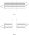
- an electroluminescent display device such as an OLED display device includes: a base substrate 10 , a display light-emitting element 11 located on the base substrate 10 , and an encapsulating layer 12 covering the display light-emitting element 11 .
- the display light-emitting element 11 may include a circuit layer 111 and an OLED device layer 112 located on the circuit layer 111 .
- the circuit layer 111 may include various circuits and conductive traces for driving the display light-emitting element
- the OLED device layer 112 may include an anode, a cathode, and various functional layers.
- various functional layers may include an electron injection layer, an electron transport layer, a hole injection layer, a hole transport layer, an organic light-emitting layer, and the like.
- the encapsulating layer 12 may include a film layer formed of an inorganic layer and an organic layer that are alternately provided.
- the encapsulating layer may include a first water blocking layer 121 , a planarization layer 122 , and a second water blocking layer 123 arranged in sequence.
- the first water blocking layer 121 and the second water blocking layer 123 may include an inorganic material
- the planarization layer 122 may include an organic material.
- the hole may be formed at a position where two dotted lines in FIG. 1 are located to obtain the structure shown in FIG. 2 , so as to reserve installation positions for hardware, such as front camera or home button, on a terminal device.
- OLED devices are very sensitive to water vapor and oxygen.
- the water vapor and oxygen invading into the device are a main factor that affects the service life of the OLED devices. Therefore, encapsulation is very important for the OLED devices.
- the water vapor and oxygen may easily invade the display light-emitting elements through a cut surface HS at the hole, as shown by the arrow in FIG. 2 , directly invade the display light-emitting elements located in the display area, resulting in encapsulation failure of OLED display device, thereby affecting display effect of the OLED display device and seriously affecting the service life of the OLED display device.
- FIG. 3 schematically shows the mask 14 used in the evaporation process.
- the mask 14 has an open mask structure, and a shielding structure cannot be formed in the opening area of the mask 14 , as a result, after punching a hole on the OLED display device subsequently, the display light-emitting elements located at the cut surface of the hole (the cut surface HS in FIG. 2 ) may not be protected by the encapsulating layer.
- the water and oxygen may enter the interior of the display light-emitting elements through the cut surface, resulting in the encapsulation failure of the OLED display device, thereby affecting the display effect of the OLED display device and seriously affecting the service life of the OLED display device.
- FIG. 4 shows a plan view of an electroluminescent display substrate according to exemplary embodiments of the present disclosure.
- FIG. 5 is a schematic cross-sectional view of an electroluminescent display substrate according to exemplary embodiments of the present disclosure taken along line AA′ in FIG. 4 .
- FIG. 6 is a partial cross-sectional view of an electroluminescent display substrate according to exemplary embodiments of the present disclosure taken along line AA′ in FIG. 4 .
- the electroluminescent display substrate includes a display area 41 and at least one hole 43 located in the display area 41 .
- two holes 43 are provided as an example for illustration. It should be understood that the embodiments of the present disclosure are not limited to this. In other embodiments, fewer (for example, one) or more holes 43 may be provided.
- the hole mentioned in this context is an area on the display substrate for installing the hardware structure.
- a name “hole” is used in this context, and the hole includes but is not limited to the following forms: through hole, groove, opening, etc.
- the hardware structure may include one or more of the following structures: a front camera, a home key, an earpiece, or a speaker.
- the specific installation method of the hardware structure is not particularly limited in the embodiments of the present disclosure.
- the shape of the hole may be determined according to the shape of the hardware structure to be installed. For example, a cross section of the hole in a direction parallel to the base substrate of the display substrate may have one or more of the following shapes: circle, ellipse, rectangle, rounded rectangle, square, diamond, trapezoid, etc.
- the display substrate includes: a base substrate 50 , and a thin film transistor (abbreviated as TFT) 51 , a display light-emitting element 52 and an encapsulating structure 53 sequentially arranged on the base substrate 50 .
- TFT thin film transistor
- the hole 43 penetrates the base substrate and various film layers on the display substrate in a direction perpendicular to the base substrate 50 .
- the display substrate is applicable for full-screen and frameless display panels.
- the display substrate may be an OLED display substrate.
- the thin film transistor may be a top-gate type TFT or a bottom-gate type TFT.
- the display light-emitting element 52 may include an anode, a light-emitting layer, and a cathode.
- the encapsulating structure 53 may be a thin film encapsulating structure (TFE).
- TFE thin film encapsulating structure
- the display substrate may also include some other film layers, for example, a conductive layer, a planarization layer, a passivation layer, etc., which will be further described below.
- the hole 43 may be arranged in the display area, that is, the hardware structure is installed in the display area, so that the frame may be reduced, the effective area of the display area may be increased, and the fabrication of a full screen may be realized.
- a rectangular area 43 located in the middle position in FIG. 5 and enclosed by the dashed frame is the position of the hole, and the hole 43 penetrates the base substrate 50 and various film layers in the direction perpendicular to the base substrate 50 (i.e., Y-axis direction in FIG. 5 ) to form the structure shown in FIG. 5 .
- the hole may also be set to only penetrate film layers except the base substrate in the Y-axis direction as required, and the specific penetrating part of the hole may be set as required, which is not specifically limited here.
- the display substrate includes at least one post spacer 45 disposed around the hole 43 .
- the post spacer 45 may block water vapor and oxygen to prevent the water vapor and oxygen from invading the display light-emitting elements through the cut surface of the hole 43 .
- FIG. 4 shows that two holes are provided.
- the hole includes a closed-ring pattern
- the post spacer 45 is arranged around the hole 43 . Therefore, the post spacer 45 also includes a closed-ring pattern.
- the shape of the post spacer 45 is consistent with the shape of the hole 43 .
- the lower hole 43 in FIG. 4 is circular and the corresponding post spacer 45 is also circular
- the upper hole 43 is rectangular and the corresponding post spacer 45 is also rectangular.
- the display substrate may be an OLED display substrate and the thin film transistor is a top-gate TFT.
- the display substrate includes a buffer layer 61 disposed on the base substrate 50 , and the thin film transistor 51 is disposed on a side of the buffer layer 61 away from the base substrate 50 .
- the thin film transistor 51 includes an active layer 511 arranged on the side of the buffer layer 61 away from the base substrate 50 , a gate insulating layer 512 arranged on a side of the active layer 511 away from the base substrate 50 , and a gate electrode 513 arranged on a side of the gate insulating layer 512 away from the base substrate 50 , an interlayer dielectric layer 514 arranged on a side of the gate electrode 513 away from the base substrate 50 and covering the gate electrode 513 , and a first conductive layer arranged on a side of the interlayer dielectric layer 514 away from the base substrate 50 .
- the first conductive layer may include a source electrode 515 and a drain electrode 516 of the thin film transistor as well as conductive plugs 517 formed in via holes penetrating the interlayer dielectric layer 514 .
- the source electrode 515 and the drain electrode 516 of the thin film transistor are electrically connected to the active layer 511 through respective conductive plugs 517 .
- the display substrate further includes a pixel defining layer 65 , and the pixel defining layer 65 defines an opening area 651 , and the display light-emitting element 52 may be located in the opening area 651 .
- the display light-emitting element 52 may include an anode 521 , a light-emitting layer 522 , and a cathode 523 , and the light-emitting layer 522 is sandwiched between the anode 521 and the cathode 523 .
- the “light-emitting layer” here is a generalized name of various functional layers of the OLED display light-emitting element, for example, it may include various functional layers such as an electron injection layer, an electron transport layer, a hole injection layer, a hole transport layer, and an organic light-emitting layer.
- the display substrate further includes various film layers arranged between the thin film transistor 51 and the display light-emitting element 52 .
- the various film layers may include a first planarization layer 62 disposed on a side of the first conductive layer away from the base substrate 50 and covering the first conductive layer, a second conductive layer 63 disposed on a side of the first planarization layer 62 away from the base substrate 50 , and a passivation layer 64 disposed on a side of the second conductive layer 63 away from the base substrate 50 and covering the second conductive layer 63 .
- the first planarization layer 62 may be composed of an organic material
- the second conductive layer 63 and the passivation layer 64 may both be composed of an inorganic material. Therefore, in this context, the second conductive layer 63 and the passivation layer 64 may be referred to as inorganic material layers.
- the second conductive layer 63 may be composed of the same conductive material as the first conductive layer.
- the second conductive layer 63 may be electrically connected to the source electrode or drain electrode of the thin film transistor through a conductive plug 621 formed in a via hole penetrating the first planarization layer 62 .
- the anode 521 or the cathode 523 may be electrically connected to the second conductive layer 63 through a conductive plug 641 formed in the via hole penetrating the passivation layer 64 .
- the second conductive layer 63 is electrically connected to the drain electrode 516
- the anode 521 is electrically connected to the second conductive layer 63 . In this way, the anode 521 and the drain electrode 516 are electrically connected.
- the encapsulating structure 53 may include film layers which include an inorganic layer and an organic layer alternately disposed, for example, it may include a first water blocking layer 531 , a second planarization layer 532 , and a second water blocking layer 533 arranged in sequence.
- the first water blocking layer 531 and the second water blocking layer 533 may be composed of an inorganic material
- the second planarization layer 532 may be composed of an organic material.
- the display substrate further includes a support layer 44 .
- the support layer 44 may be disposed on the side of the interlayer dielectric layer 514 away from the base substrate 50 to support the post spacer 45 .
- the support layer 44 may be located in the same layer as the first planarization layer 62 .
- the post spacer 45 is disposed on the support layer 44 .
- the post spacer 45 may be disposed on a surface of the support layer 44 away from the interlayer dielectric layer 514 , and a surface of the post spacer 45 facing the support layer 44 may be in contact with a surface of the support layer 44 away from interlayer the dielectric layer 514 .
- An orthographic projection of the post spacer 45 on the base substrate 50 falls within an orthographic projection of the support layer 44 on the base substrate 50 .
- the display substrate further includes an overcoat layer 46 covering the post spacer 45 .
- the overcoat layer 46 may be made of an inorganic material, and the overcoat layer 46 covers side surfaces of the post spacer 45 and a surface of the post spacer 45 away from the support layer 44 . That is, the overcoat layer 46 contacts a first side surface of the post spacer 45 close to the hole 43 , a second side surface of the post spacer 45 away from the hole 43 , and the surface of the post spacer 45 away from the base substrate (that is, a top surface of the post spacer 45 ). As shown in FIGS.
- an orthographic projection of the overcoat layer 46 on the base substrate 50 covers the orthographic projection of the post spacer 45 on the base substrate 50 .
- the post spacer 45 is formed as a water blocking structure as a whole to further prevent water vapor and oxygen from invading the display light-emitting elements through the cut surface of the hole 43 .
- the material of the post spacer 45 may be photoresist, such as a negative photoresist, and the pattern of the post spacer 45 may be obtained through a photolithography process.
- the overcoat layer 46 may have a single-layer structure, and the overcoat layer 46 may be located in the same layer as the second conductive layer 63 .
- the overcoat layer 46 and the second conductive layer 63 may be made of the same material as the source electrode and drain electrode of the thin film transistor. In this way, the overcoat layer 46 and the second conductive layer 63 may be formed of the same material and through the same patterning process, that is, there is no need to increase the number of patterning processes to form the overcoat layer separately, which is beneficial to save the number of patterning processes and to reduce the manufacturing difficulty and cost.
- the overcoat layer 46 may have a single-layer structure, and the overcoat layer 46 may be located in the same layer as the passivation layer 64 .
- the overcoat layer 46 and the passivation layer 64 may be composed of an inorganic material such as silicon oxide, silicon nitride, and the like. In this way, the overcoat layer 46 and the passivation layer 64 may be formed of the same material and through the same patterning process, that is, there is no need to increase the number of patterning processes to form the overcoat layer separately, which is beneficial to save the number of patterning processes and to reduce the manufacturing difficulty and cost.
- the overcoat layer 46 may have a multilayer structure, and the overcoat layer 46 may include a first overcoat sub-layer 461 and a second overcoat sub-layer 462 , wherein the first overcoat sub-layer 461 may be located in the same layer as the second conductive layer 63 , and the second overcoat sub-layer 462 may be located in the same layer as the passivation layer 64 .
- the first overcoat sub-layer 461 and the second conductive layer 63 may be formed of the same material and through the same patterning process
- the second overcoat sub-layer 462 and the passivation layer 64 may be formed of the same material and through the same patterning process.
- a laminated structure including the support layer, the post spacer and the overcoat layer is formed. Since the support layer is provided under the post spacer, it is advantageous for the overcoat layer provided in the same layer as the inorganic material layer to cover the post spacer, thereby facilitating that the post spacer as a whole is formed into a water blocking structure.
- the cathode 523 of the light-emitting element 52 is also formed on the overcoat layer 46 , that is, an orthographic projection of the cathode 523 of the light-emitting element 52 on the base substrate 50 overlaps with an orthographic projection of the overcoat layer 46 on the base substrate 50 .
- the orthographic projection of the cathode 523 of the display light-emitting element 52 on the base substrate 50 overlaps with the orthographic projection of the post spacer 45 on the base substrate 50 .
- the light-emitting layer 522 and the cathode 523 of the display light-emitting element 52 are further formed on the overcoat layer 46 , that is, an orthographic projection of each of the light-emitting layer 522 and the cathode 523 of the display light-emitting element 52 on the base substrate 50 overlaps with the orthographic projection of the overcoat layer 46 on the base substrate 50 .
- the orthographic projection of each of the light-emitting layer 522 and the cathode 523 of the display light-emitting element 52 on the base substrate 50 overlaps with the orthographic projection of the post spacer 45 on the base substrate 50 .
- the cross section of the post spacer 45 in the direction perpendicular to the base substrate 50 may have an inverted trapezoid shape, that is, an area of the cross section of the post spacer 45 in the direction parallel to the base substrate 50 gradually increases.
- the various film layers of the display light-emitting element 52 may be disconnected at the post spacer 45 , for example, as shown in FIGS. 6 - 8 , the cathode 523 of the display light-emitting element 52 is disconnected at the post spacer 45 .
- both the light-emitting layer 522 and the cathode 523 of the display light-emitting element 52 may be disconnected at the post spacer 45 . Therefore, the water vapor and oxygen will not penetrate the interior of the display light-emitting element along the film layer (such as the light-emitting layer or the cathode) of the display light-emitting element through the cut surface of the hole 43 , which further improves the encapsulating reliability of the display light-emitting elements.
- the cross section of the post spacer 45 in the direction perpendicular to the base substrate 50 may have other shapes, for example, I-shape shown in FIG. 9 A and T-shape shown in FIG. 9 B . That is, there is a convex structure on a side surface of the post spacer 45 .
- a cross section of the post spacer 45 in the direction parallel to the base substrate 50 at a first position has a first cross-sectional area
- a cross section of the post spacer 45 in the direction parallel to the base substrate 50 at a second position has a second cross-sectional area
- the first position is farther away from the support layer 44 than the second position
- the first cross-sectional area is larger than the second cross-sectional area.
- respective film layers of the display light-emitting element 52 are disconnected at the post spacer 45 .
- the light-emitting layer 522 and the cathode 523 of the display light-emitting element 52 are disconnected at the post spacer 45 . Therefore, the water vapor and oxygen may not invade the interior of the display light-emitting element along the film layers of the display light-emitting element through the cut surface of the hole 43 , which further improves the encapsulating reliability of the display light-emitting elements.
- the encapsulating structure 53 may cover the post spacer 45 and the overcoat layer 46 .
- the first water blocking layer 531 and the second water blocking layer 533 of the encapsulating structure 53 cover the post spacer 45 and the overcoat layer 46 .
- each of the first water blocking layer 531 , the second planarization layer 532 , and the second water blocking layer 533 of the encapsulating structure 53 is located above the display light-emitting elements 52 to cover the display light-emitting elements 52 .
- an orthographic projection of each film layer of the display light-emitting element 52 on the base substrate 50 falls within an orthographic projection of each of the first water blocking layer 531 , the second planarization layer 532 , and the second water blocking layer 533 on the base substrate 50 .
- the encapsulating structure 53 may encapsulate the display light-emitting element 52 .
- first water blocking layer 531 and the second water blocking layer 533 of the encapsulating structure 53 extend from a position above the display light-emitting elements 52 to an edge of the hole 43 , so that the orthographic projection of each of the support layer 44 , the post spacer 45 and the overcoat layer 46 on the base substrate 50 falls within the orthographic projection of each of the first water blocking layer 531 and the second water blocking layer 533 of the encapsulating structure 53 on the base substrate 50 .
- the water vapor and oxygen may be better prevented from invading the interior of the display light-emitting element through the cut surface of the hole 43 , which further improves the encapsulating reliability of the display light-emitting elements.
- one hole 43 may be surrounded by two post spacers 45 to improve the ability of the post spacers to prevent water and oxygen from invading.
- the embodiments of the present disclosure are not limited to this, and fewer post spacers 45 (for example, one) or more post spacers 45 may be provided to surround one hole 43 according to actual needs.
- the overcoat layer 46 covers the side surfaces of each post spacer 45 and the surface of each post spacer 45 away from the support layer 44 . As shown in FIGS.
- the orthographic projection of the overcoat layer 46 on the base substrate 50 covers the orthographic projection of each post spacer 45 on the base substrate 50 .
- the post spacer 45 is integrally formed as a water blocking structure to further prevent water vapor and oxygen from invading the display light-emitting elements through the cut surface of the hole 43 .
- a post spacer 45 close to the hole 43 may be referred to as a first post spacer 451
- a post spacer 45 distal to the hole 43 may be referred to as a second post spacer 452 . That is, the first post spacer 451 is closer to the hole 43 than the second post spacer 452 .
- the second planarization layer 532 of the encapsulating structure 53 extends from a position above the display light-emitting elements 52 to a position above the second post spacer 452 , for example, the second planarization layer 532 may extend to a position where a side surface of the second post spacer 452 away from the hole 43 is located, that is, an orthographic projection of each of the first post spacer 451 and the second post spacer 452 on the base substrate 50 does not completely fall within the orthographic projection of the second planarization layer 532 on the base substrate 50 .
- the second planarization layer 532 of the encapsulating structure 53 extends from a position above the display light-emitting elements 52 to a position close to above the first post spacer 451 .
- the second planarization layer 532 may extend to a position where a side surface of the first post spacer 451 away from the hole 43 is located, that is, the orthographic projection of the first post spacer 451 on the base substrate 50 does not fall within the orthographic projection of the second planarization layer 532 on the base substrate 50 .
- the second planarization layer 532 of the encapsulating structure 53 does not cover the post spacer closest to the hole 43 , and the second planarization layer 532 of the encapsulating structure 53 extends to a position above the post spacer closest to the hole 43 , therefore, the second planarization layer 532 does not extend to the cut surface of the hole 43 .
- the second planarization layer 532 is made of an organic material, and the water vapor and oxygen may easily invade the interior of the display light-emitting elements through the organic material.
- the second planarization layer 532 Since the second planarization layer 532 is disconnected at the post spacer, it may better prevent the water vapor and oxygen from invading the interior of the display light-emitting elements through the cut surface of the hole 43 , which further improves the encapsulating reliability of the display light-emitting elements. Moreover, the material for forming the second planarization layer 532 may be saved, and the hole 43 may be formed more easily by cutting.
- FIGS. 11 A and 11 B are respectively partial enlarged views of a cross-sectional view of a display substrate according to embodiments of the present disclosure, which mainly show the shape and relative positional relationship of the support layer and the post spacer.
- two post spacers 451 and 452 may share one support layer 44 .
- the cross section of the support layer 44 in the direction perpendicular to the base substrate 50 may have a regular trapezoidal shape, that is, the area of the cross section of the support layer 44 in the direction parallel to the base substrate 50 gradually decreases in a direction away from the base substrate 50 .
- Two post spacers 451 , 452 or more post spacers are arranged on one support layer 44 , and orthographic projections of the two post spacers 451 , 452 or more post spacers on the base substrate 50 fall within the orthographic projection of the one support layer 44 on the base substrate 50 .
- the two post spacers 451 and 452 may each have a respective support layer.
- the support layer 44 may include a first support sub-layer 441 and a second support sub-layer 442 , and the first support sub-layer 441 and the second support sub-layer 442 are located in the same layer.
- a cross section of each of the first support sub-layer 441 and the second support sub-layer 442 in the direction perpendicular to the base substrate 50 may have a regular trapezoidal or convex arc shape, that is, an area of the cross section of each of the first support sub-layer 441 and the second support sub-layer 442 in the direction parallel to the base substrate 50 gradually decreases in a direction away from the base substrate 50 .
- the two post spacers 451 , 452 or more post spacers are arranged on the respective support sub-layers, and the orthographic projections of the two post spacers 451 , 452 or more post spacers on the base substrate 50 fall with orthographic projections of respective support sub-layers 441 , 442 on the base substrate 50 .
- a corner of the overcoat layer 46 covering the post spacer at a junction position where the post spacer is connected with the support sub-layer may have an obtuse angle, as shown by angle ⁇ in the drawing.
- corners of the first water blocking layer 531 and the second water blocking layer 533 covering the post spacer at the junction position where the post spacer is connected with the support sub-layer are also obtuse angles.
- the overcoat layer 46 , the first water blocking layer 531 , and the second water blocking layer 533 are not prone to stress concentration problems at the corners, thereby the overcoat layer 46 , the first water blocking layer 531 , and the second water blocking layer 533 are prevented from generating cracks at the corners. Therefore, with such a setting manner, the encapsulating reliability may be further improved.
- the display substrate may further include conductive traces 47 .
- the conductive traces 47 may be located in the first conductive layer, that is, the conductive traces 47 may be located in the same layer as the source electrode and drain electrode of the thin film transistor.
- the display substrate may further include a blocking structure 48 .
- the blocking structure 48 may be disposed between the hole 43 and the post spacer 45 , that is, an orthographic projection of the blocking structure 48 on the base substrate 50 is located between the orthographic projection of the hole 43 on the base substrate 50 and the orthographic projection of the post spacer 45 on the base substrate 50 .
- the blocking structure 48 is also called a crack dam, and configured to block cracks from extending to the display light-emitting elements of the display substrate, thereby further improving the encapsulating reliability.
- the blocking structure 48 may include a trench (i.e., a recess) provided in an insulating layer (for example, a gate insulating layer, an interlayer insulating layer, etc.) to form a crack dam for blocking expansion of cracks.
- the blocking structure 48 may include a blocking dam (i.e., a protrusion), which may be provided in the same layer as metal conductive layer (for example, a gate electrode) to form a crack dam for blocking the expansion of the cracks.
- a recess or a protrusion may also be formed to block the expansion of the cracks.
- FIG. 12 is a flowchart of a manufacturing method of an electroluminescent display substrate according to embodiments of the present disclosure. With reference to FIGS. 6 - 8 and FIG. 12 , the manufacturing method may be performed according to the following steps. It should be noted that, according to some embodiments of the present disclosure, some of the following steps may be executed individually or in combination, and may be executed in parallel or sequentially, and are not limited to the specific operation sequence described below.
- step S 101 various film layers of the thin film transistor are sequentially formed on the base substrate 50 to form the thin film transistor 51 .
- a support layer 44 is formed on the base substrate 50 .
- a planarization film layer may be formed on the side of the thin film transistor 51 away from the base substrate 50 , and the first planarization layer 62 and the support layer 44 may be formed through one patterning process.
- a post spacer 45 is formed on a side of the support layer 44 away from the base substrate 50 .
- the material of the post spacer 45 may be photoresist, such as a negative photoresist, and the post spacer 45 may be obtained through a photolithography process.
- the cross section of the post spacer 45 in a direction perpendicular to the base substrate 50 may have an inverted trapezoid shape, an I-shape or a T-shape. That is, there is a convex structure on the side surface of the post spacer 45 , that is, a cross section of the post spacer 45 in the direction parallel to the base substrate 50 at a first position has a first cross-sectional area, the cross section of the post spacer 45 in the direction parallel to the base substrate 50 at a second position has a second cross-sectional area, the first position is farther away from the support layer 44 than the second position, and the first cross-sectional area is larger than the second cross-sectional area.
- step S 104 an overcoat layer is formed on a side of the post spacer 45 away from the base substrate 50 .
- a conductive material film layer may be formed on a side of the first planarization layer 62 and the post spacer 45 away from the base substrate 50 , and the second conductive layer 63 and the overcoat layer 46 may be formed by one patterning process.
- the second conductive layer 63 is electrically connected to the source electrode or drain electrode of the thin film transistor, and the overcoat layer 46 covers the post spacer 45 and the support layer 44 .
- a passivation material film layer may be formed on a side of the second conductive layer 63 away from the base substrate 50 , and the passivation layer 64 and the overcoat layer 46 may be formed through one patterning process.
- the passivation layer 64 covers the second conductive layer 63
- the overcoat layer 46 covers the post spacer 45 and the support layer 44 .
- a conductive material film layer may be formed on a side of the first planarization layer 62 and the post spacer 45 away from the base substrate 50 , and the second conductive layer 63 and the first overcoat sub-layer 461 may be formed through one patterning process.
- the second conductive layer 63 is electrically connected to the source electrode or drain electrode of the thin film transistor, and the first overcoat sub-layer 461 covers the post spacer 45 and the support layer 44 .
- a passivation material film layer is formed on a side of the second conductive layer 63 and the first overcoat sub-layer 461 away from the base substrate 50 , and the passivation layer 64 and the second overcoat sub-layer 462 are formed through one patterning process.
- the passivation layer 64 covers the second conductive layer 63
- the second overcoat sub-layer 462 covers the post spacer 45 and the support layer 44 .
- step S 105 various film layers of the display light-emitting element 52 are formed on a side of the passivation layer 64 and the overcoat layer 46 away from the base substrate 50 .
- the anode, the light-emitting layer, and the cathode of the display light-emitting element 52 may be sequentially formed, and the anode, the light-emitting layer, and the cathode of the display light-emitting element 52 may not be formed at a position where the hole is to be formed.
- the light-emitting layer and the cathode of the display light-emitting element 52 may be formed by an evaporation process.
- the post spacer 45 has a structure of wide top and narrow bottom, the light-emitting layer and the cathode of the display light-emitting element 52 may be disconnected at the post spacer 45 to prevent the water vapor and oxygen from invading the interior of the display light-emitting elements along the film layers of the display light-emitting elements.
- step S 106 an encapsulating structure 53 is formed on the base substrate 50 .
- the encapsulating structure 53 may include a first water blocking layer 531 , a second planarization layer 532 , and a second water blocking layer 533 arranged in sequence.
- the first water blocking layer 531 and the second water blocking layer 533 may be composed of an inorganic material
- the second planarization layer 532 may be composed of an organic material.
- the first water blocking layer 531 and the second water blocking layer 533 cover the post spacer 45
- the second planarization layer 532 of the encapsulating structure 53 does not cover at least the post spacer closest to the hole 43 .
- step S 107 a hole 43 is formed in an area surrounded by the post spacer 45 .
- laser, stamping, or other cutting methods may be used to remove portions of respective film layers and the base substrate in the area surrounded by the post spacer 45 to form the hole 43 .
- the support layer, the overcoat layer and other film layers may be formed through the same patterning process as the planarization layer, the conductive layer or the passivation layer. In this way, the encapsulating reliability of the display substrate may be improved without changing the existing process flow, which is beneficial to save equipment investment and reduce manufacturing costs.
- the material of the post spacer may be selected as required, and the embodiments of the present disclosure do not intend to limit it.
- the post spacer may be fabricated through a separate step, or may be fabricated together with other film layers.
- the pattern of the planarization layer may not be formed at the position corresponding to the hole to be formed, so that the material for the planarization layer may be saved, and the hole may be more easily formed by cutting.
- the pattern of the planarization layer may be formed by inkjet printing.
- a blocking structure 48 may also be formed between the hole and the corresponding post spacer.
- the above-mentioned manufacturing method provided by the embodiments of the present disclosure should have the same characteristics and advantages as the display substrate provided by the embodiments of the present disclosure. Therefore, the characteristics and advantages of the above-mentioned manufacturing method provided by the embodiments of the present disclosure may be referred to the characteristics and advantages of the display substrate described above, which will not be repeated here.
- embodiments of the present disclosure also provide a display device, including the electroluminescent display substrate provided by the above-mentioned embodiments.
- the display device 130 may include the display substrate described in any one of the above embodiments, and in particular, it may be a type of display device with at least one hole.
- the display device may be any product or part with a display function, such as a smart phone, a wearable smart watch, smart glasses, a tablet computer, a television, a monitor, a notebook computer, a digital photo frame, a navigator, a car monitor, an e-book, etc.
Landscapes
- Engineering & Computer Science (AREA)
- Manufacturing & Machinery (AREA)
- Physics & Mathematics (AREA)
- Optics & Photonics (AREA)
- Microelectronics & Electronic Packaging (AREA)
- Electroluminescent Light Sources (AREA)
- Devices For Indicating Variable Information By Combining Individual Elements (AREA)
Abstract
Description
Claims (18)
Applications Claiming Priority (3)
| Application Number | Priority Date | Filing Date | Title |
|---|---|---|---|
| CN201910475322.4 | 2019-05-31 | ||
| CN201910475322.4A CN110212113B (en) | 2019-05-31 | 2019-05-31 | Electroluminescent display substrate, preparation method thereof and electroluminescent display device |
| PCT/CN2020/083256 WO2020238412A1 (en) | 2019-05-31 | 2020-04-03 | Electroluminescent display substrate and preparation method therefor, and electroluminescent display apparatus |
Publications (2)
| Publication Number | Publication Date |
|---|---|
| US20210273194A1 US20210273194A1 (en) | 2021-09-02 |
| US12041808B2 true US12041808B2 (en) | 2024-07-16 |
Family
ID=67790275
Family Applications (1)
| Application Number | Title | Priority Date | Filing Date |
|---|---|---|---|
| US17/255,107 Active 2042-05-26 US12041808B2 (en) | 2019-05-31 | 2020-04-03 | Electroluminescent display substrate, manufacturing method thereof, and electroluminescent display device |
Country Status (3)
| Country | Link |
|---|---|
| US (1) | US12041808B2 (en) |
| CN (1) | CN110212113B (en) |
| WO (1) | WO2020238412A1 (en) |
Families Citing this family (29)
| Publication number | Priority date | Publication date | Assignee | Title |
|---|---|---|---|---|
| US11575102B2 (en) | 2019-03-26 | 2023-02-07 | Chengdu Boe Optoelectronics Technology Go., Ltd. | Display substrate, preparation method thereof and display device |
| CN112838167B (en) * | 2019-11-22 | 2025-01-10 | 京东方科技集团股份有限公司 | Display substrate and manufacturing method thereof |
| CN110212113B (en) * | 2019-05-31 | 2021-11-09 | 京东方科技集团股份有限公司 | Electroluminescent display substrate, preparation method thereof and electroluminescent display device |
| CN110265583B (en) * | 2019-07-26 | 2022-08-12 | 京东方科技集团股份有限公司 | A display panel, method of making the same, and display device |
| CN110610972B (en) * | 2019-09-19 | 2022-06-03 | 京东方科技集团股份有限公司 | Display substrate, preparation method thereof and display device |
| CN110729334B (en) | 2019-10-22 | 2022-10-18 | 京东方科技集团股份有限公司 | Electroluminescent display substrate and display device |
| CN110783488B (en) * | 2019-10-31 | 2022-08-16 | 京东方科技集团股份有限公司 | Display substrate, manufacturing method thereof, display device and electronic watch |
| CN110767735B (en) * | 2019-11-06 | 2022-06-03 | 京东方科技集团股份有限公司 | Manufacturing method of display panel, display panel and display |
| CN110867526B (en) * | 2019-11-25 | 2023-04-18 | 京东方科技集团股份有限公司 | Display substrate, preparation method thereof and display device |
| JP7485484B2 (en) * | 2019-12-11 | 2024-05-16 | 京東方科技集團股▲ふん▼有限公司 | Display substrate, its manufacturing method, and display device |
| CN111129103A (en) * | 2020-01-02 | 2020-05-08 | 昆山国显光电有限公司 | Display panel and display device |
| CN111180465B (en) * | 2020-01-03 | 2022-09-23 | 京东方科技集团股份有限公司 | Display panel, preparation method and display device |
| CN111180496B (en) * | 2020-01-06 | 2023-07-04 | 京东方科技集团股份有限公司 | Display substrate, preparation method thereof, display panel and display device |
| CN211719594U (en) * | 2020-02-21 | 2020-10-20 | 京东方科技集团股份有限公司 | A display panel and display device |
| WO2021184273A1 (en) * | 2020-03-18 | 2021-09-23 | 京东方科技集团股份有限公司 | Display substrate and manufacturing method therefor, and display apparatus |
| CN111341210A (en) | 2020-04-09 | 2020-06-26 | 京东方科技集团股份有限公司 | Display panel, display device, and manufacturing method of display panel |
| US11864413B2 (en) * | 2020-05-15 | 2024-01-02 | Chengdu Boe Optoelectronics Technology Co., Ltd. | Display substrate and method for manufacturing the same, display device |
| CN113745269B (en) * | 2020-05-27 | 2024-10-18 | 京东方科技集团股份有限公司 | Display substrate and manufacturing method thereof, display panel, and display device |
| TWI727900B (en) * | 2020-10-06 | 2021-05-11 | 友達光電股份有限公司 | Display panel |
| KR102852522B1 (en) | 2020-11-25 | 2025-09-02 | 삼성디스플레이 주식회사 | Display device and method of manufacturing the same |
| CN116324949A (en) * | 2021-07-28 | 2023-06-23 | 京东方科技集团股份有限公司 | Display substrate, display device |
| CN113838952B (en) * | 2021-09-06 | 2023-10-27 | 厦门乾照半导体科技有限公司 | Nano-LED application-based epitaxial structure, chip and preparation method |
| CN116053280B (en) * | 2021-10-27 | 2025-04-18 | 京东方科技集团股份有限公司 | A display panel, a manufacturing method thereof and a display device |
| CN114077108B (en) * | 2021-11-19 | 2023-11-07 | 京东方科技集团股份有限公司 | Display panel and display device |
| CN114551553A (en) * | 2022-02-25 | 2022-05-27 | 合肥京东方卓印科技有限公司 | Display substrate and display device |
| CN114628613B (en) * | 2022-03-22 | 2025-01-28 | 京东方科技集团股份有限公司 | Display panel and display device |
| CN114784081A (en) * | 2022-05-27 | 2022-07-22 | 广州华星光电半导体显示技术有限公司 | Display panel and manufacturing method thereof |
| CN115347133A (en) * | 2022-08-26 | 2022-11-15 | 北京京东方技术开发有限公司 | Display substrate, preparation method thereof and display panel |
| CN119072150A (en) * | 2023-05-31 | 2024-12-03 | 京东方科技集团股份有限公司 | Display panel and manufacturing method thereof, and display device |
Citations (10)
| Publication number | Priority date | Publication date | Assignee | Title |
|---|---|---|---|---|
| CN106601781A (en) | 2017-01-25 | 2017-04-26 | 上海天马微电子有限公司 | Organic light emitting display panel and display device |
| CN107068715A (en) | 2017-03-28 | 2017-08-18 | 上海天马微电子有限公司 | Organic light-emitting display panel, organic light-emitting display device and preparation method of organic light-emitting display panel |
| CN107452894A (en) | 2017-07-31 | 2017-12-08 | 京东方科技集团股份有限公司 | A kind of organic EL display panel, its preparation method and display device |
| CN107808896A (en) | 2017-10-27 | 2018-03-16 | 上海天马微电子有限公司 | Display panel, manufacturing method of display panel and display device |
| US20180151834A1 (en) * | 2016-11-28 | 2018-05-31 | Japan Display Inc. | Display device |
| US20180151838A1 (en) | 2016-11-29 | 2018-05-31 | Lg Display Co., Ltd. | Organic light-emitting display device |
| CN108649133A (en) | 2018-03-30 | 2018-10-12 | 上海天马微电子有限公司 | Organic light emitting display panel, method of manufacturing the same, and organic light emitting display device |
| CN108962947A (en) | 2018-07-04 | 2018-12-07 | 上海天马微电子有限公司 | Flexible display panel and display device |
| CN110212113A (en) | 2019-05-31 | 2019-09-06 | 京东方科技集团股份有限公司 | Electroluminescent display substrate and preparation method thereof, el display device |
| US20200313102A1 (en) * | 2019-03-27 | 2020-10-01 | Samsung Display Co., Ltd. | Display device |
-
2019
- 2019-05-31 CN CN201910475322.4A patent/CN110212113B/en active Active
-
2020
- 2020-04-03 WO PCT/CN2020/083256 patent/WO2020238412A1/en not_active Ceased
- 2020-04-03 US US17/255,107 patent/US12041808B2/en active Active
Patent Citations (14)
| Publication number | Priority date | Publication date | Assignee | Title |
|---|---|---|---|---|
| US20180151834A1 (en) * | 2016-11-28 | 2018-05-31 | Japan Display Inc. | Display device |
| US20180151838A1 (en) | 2016-11-29 | 2018-05-31 | Lg Display Co., Ltd. | Organic light-emitting display device |
| CN106601781A (en) | 2017-01-25 | 2017-04-26 | 上海天马微电子有限公司 | Organic light emitting display panel and display device |
| US20180061910A1 (en) | 2017-03-28 | 2018-03-01 | Shanghai Tianma Micro-electronics Co., Ltd. | Organic Light-Emitting Display Panel, Device And Method For Manufacturing The Same |
| CN107068715A (en) | 2017-03-28 | 2017-08-18 | 上海天马微电子有限公司 | Organic light-emitting display panel, organic light-emitting display device and preparation method of organic light-emitting display panel |
| US10566394B2 (en) | 2017-03-28 | 2020-02-18 | Shanghai Tianma Micro-electronics Co., Ltd. | Organic light-emitting display panel, device and method for manufacturing the same |
| CN107452894A (en) | 2017-07-31 | 2017-12-08 | 京东方科技集团股份有限公司 | A kind of organic EL display panel, its preparation method and display device |
| CN107808896A (en) | 2017-10-27 | 2018-03-16 | 上海天马微电子有限公司 | Display panel, manufacturing method of display panel and display device |
| CN108649133A (en) | 2018-03-30 | 2018-10-12 | 上海天马微电子有限公司 | Organic light emitting display panel, method of manufacturing the same, and organic light emitting display device |
| US20180342700A1 (en) | 2018-03-30 | 2018-11-29 | Shanghai Tianma Micro-electronics Co., Ltd. | Organic light-emitting display panel, method for manufacturing organic light-emitting display panel and organic light-emitting display device |
| US10224508B2 (en) | 2018-03-30 | 2019-03-05 | Shanghai Tianma Micro-electronics Co., Ltd. | Organic light-emitting display panel, method for manufacturing organic light-emitting display panel and organic light-emitting display device |
| CN108962947A (en) | 2018-07-04 | 2018-12-07 | 上海天马微电子有限公司 | Flexible display panel and display device |
| US20200313102A1 (en) * | 2019-03-27 | 2020-10-01 | Samsung Display Co., Ltd. | Display device |
| CN110212113A (en) | 2019-05-31 | 2019-09-06 | 京东方科技集团股份有限公司 | Electroluminescent display substrate and preparation method thereof, el display device |
Non-Patent Citations (1)
| Title |
|---|
| First Office Action, including Search Report, for Chinese Patent Application No. 201910475322.4, dated Dec. 25, 2020, 15 pages. |
Also Published As
| Publication number | Publication date |
|---|---|
| CN110212113B (en) | 2021-11-09 |
| CN110212113A (en) | 2019-09-06 |
| WO2020238412A1 (en) | 2020-12-03 |
| US20210273194A1 (en) | 2021-09-02 |
Similar Documents
| Publication | Publication Date | Title |
|---|---|---|
| US12041808B2 (en) | Electroluminescent display substrate, manufacturing method thereof, and electroluminescent display device | |
| US11871605B2 (en) | Display panel and manufacturing method thereof, display device | |
| US11257957B2 (en) | Thin film transistor, method of fabricating the same, array substrate and display device | |
| US11569472B2 (en) | Electroluminescent display substrate, manufacturing method thereof and electroluminescent display apparatus | |
| US11943979B2 (en) | Array substrate and fabrication method thereof, array substrate motherboard and display device | |
| US11882716B2 (en) | Display panel, method for manufacturing same, and display apparatus | |
| US20160043116A1 (en) | Thin film transistor and manufacturing method thereof, array substrate and manufacturing method thereof and display device | |
| KR20170075113A (en) | Mask assembly for thin film deposition | |
| US10333002B2 (en) | Thin film transistor and manufacturing method thereof, array substrate and manufacturing method thereof, and display device | |
| US11903276B2 (en) | Display panel, manufacturing method therefor, and display device | |
| US20200251678A1 (en) | Organic electroluminescent display panel, manufacturing method thereof and display device | |
| US20250380591A1 (en) | Array Substrate, Manufacturing Method Therefor, and Display Apparatus | |
| US12507479B2 (en) | Array substrate and display panel | |
| US20240234428A9 (en) | Array substrate, manufacturing method thereof, and display panel | |
| US20240114730A1 (en) | Display panel and manufacturing method thereof | |
| CN114792694A (en) | Thin film transistor array substrate, preparation method thereof and display panel | |
| CN118870873A (en) | Display panel and manufacturing method thereof, and display device | |
| CN111312732A (en) | Display panel, manufacturing method thereof, display module and electronic device | |
| CN115347003B (en) | Display substrate, manufacturing method thereof, and display device | |
| CN120916482A (en) | Array substrate and display panel | |
| CN111883483A (en) | Preparation method of array substrate |
Legal Events
| Date | Code | Title | Description |
|---|---|---|---|
| AS | Assignment |
Owner name: BOE TECHNOLOGY GROUP CO., LTD., CHINA Free format text: ASSIGNMENT OF ASSIGNORS INTEREST;ASSIGNORS:XIE, CHUNYAN;ZHANG, SONG;ZHANG, ZIYU;REEL/FRAME:054725/0306 Effective date: 20201014 |
|
| FEPP | Fee payment procedure |
Free format text: ENTITY STATUS SET TO UNDISCOUNTED (ORIGINAL EVENT CODE: BIG.); ENTITY STATUS OF PATENT OWNER: LARGE ENTITY |
|
| STPP | Information on status: patent application and granting procedure in general |
Free format text: DOCKETED NEW CASE - READY FOR EXAMINATION |
|
| STPP | Information on status: patent application and granting procedure in general |
Free format text: NON FINAL ACTION MAILED |
|
| STPP | Information on status: patent application and granting procedure in general |
Free format text: RESPONSE TO NON-FINAL OFFICE ACTION ENTERED AND FORWARDED TO EXAMINER |
|
| STPP | Information on status: patent application and granting procedure in general |
Free format text: NOTICE OF ALLOWANCE MAILED -- APPLICATION RECEIVED IN OFFICE OF PUBLICATIONS |
|
| STPP | Information on status: patent application and granting procedure in general |
Free format text: PUBLICATIONS -- ISSUE FEE PAYMENT RECEIVED |
|
| STPP | Information on status: patent application and granting procedure in general |
Free format text: PUBLICATIONS -- ISSUE FEE PAYMENT VERIFIED |
|
| STCF | Information on status: patent grant |
Free format text: PATENTED CASE |