US12040720B2 - Resonance conversion device and universal serial bus circuit - Google Patents
Resonance conversion device and universal serial bus circuit Download PDFInfo
- Publication number
- US12040720B2 US12040720B2 US17/704,442 US202217704442A US12040720B2 US 12040720 B2 US12040720 B2 US 12040720B2 US 202217704442 A US202217704442 A US 202217704442A US 12040720 B2 US12040720 B2 US 12040720B2
- Authority
- US
- United States
- Prior art keywords
- switch
- voltage
- signal
- coupled
- output voltage
- Prior art date
- Legal status (The legal status is an assumption and is not a legal conclusion. Google has not performed a legal analysis and makes no representation as to the accuracy of the status listed.)
- Active, expires
Links
Images


Classifications
-
- H—ELECTRICITY
- H02—GENERATION; CONVERSION OR DISTRIBUTION OF ELECTRIC POWER
- H02M—APPARATUS FOR CONVERSION BETWEEN AC AND AC, BETWEEN AC AND DC, OR BETWEEN DC AND DC, AND FOR USE WITH MAINS OR SIMILAR POWER SUPPLY SYSTEMS; CONVERSION OF DC OR AC INPUT POWER INTO SURGE OUTPUT POWER; CONTROL OR REGULATION THEREOF
- H02M3/00—Conversion of DC power input into DC power output
- H02M3/22—Conversion of DC power input into DC power output with intermediate conversion into AC
- H02M3/24—Conversion of DC power input into DC power output with intermediate conversion into AC by static converters
- H02M3/28—Conversion of DC power input into DC power output with intermediate conversion into AC by static converters using discharge tubes with control electrode or semiconductor devices with control electrode to produce the intermediate AC
- H02M3/325—Conversion of DC power input into DC power output with intermediate conversion into AC by static converters using discharge tubes with control electrode or semiconductor devices with control electrode to produce the intermediate AC using devices of a triode or a transistor type requiring continuous application of a control signal
- H02M3/335—Conversion of DC power input into DC power output with intermediate conversion into AC by static converters using discharge tubes with control electrode or semiconductor devices with control electrode to produce the intermediate AC using devices of a triode or a transistor type requiring continuous application of a control signal using semiconductor devices only
- H02M3/33569—Conversion of DC power input into DC power output with intermediate conversion into AC by static converters using discharge tubes with control electrode or semiconductor devices with control electrode to produce the intermediate AC using devices of a triode or a transistor type requiring continuous application of a control signal using semiconductor devices only having several active switching elements
-
- H—ELECTRICITY
- H02—GENERATION; CONVERSION OR DISTRIBUTION OF ELECTRIC POWER
- H02M—APPARATUS FOR CONVERSION BETWEEN AC AND AC, BETWEEN AC AND DC, OR BETWEEN DC AND DC, AND FOR USE WITH MAINS OR SIMILAR POWER SUPPLY SYSTEMS; CONVERSION OF DC OR AC INPUT POWER INTO SURGE OUTPUT POWER; CONTROL OR REGULATION THEREOF
- H02M1/00—Details of apparatus for conversion
- H02M1/0003—Details of control, feedback or regulation circuits
- H02M1/0025—Arrangements for modifying reference values, feedback values or error values in the control loop of a converter
-
- H—ELECTRICITY
- H02—GENERATION; CONVERSION OR DISTRIBUTION OF ELECTRIC POWER
- H02M—APPARATUS FOR CONVERSION BETWEEN AC AND AC, BETWEEN AC AND DC, OR BETWEEN DC AND DC, AND FOR USE WITH MAINS OR SIMILAR POWER SUPPLY SYSTEMS; CONVERSION OF DC OR AC INPUT POWER INTO SURGE OUTPUT POWER; CONTROL OR REGULATION THEREOF
- H02M1/00—Details of apparatus for conversion
- H02M1/0003—Details of control, feedback or regulation circuits
- H02M1/0032—Control circuits allowing low power mode operation, e.g. in standby mode
- H02M1/0035—Control circuits allowing low power mode operation, e.g. in standby mode using burst mode control
-
- H—ELECTRICITY
- H02—GENERATION; CONVERSION OR DISTRIBUTION OF ELECTRIC POWER
- H02M—APPARATUS FOR CONVERSION BETWEEN AC AND AC, BETWEEN AC AND DC, OR BETWEEN DC AND DC, AND FOR USE WITH MAINS OR SIMILAR POWER SUPPLY SYSTEMS; CONVERSION OF DC OR AC INPUT POWER INTO SURGE OUTPUT POWER; CONTROL OR REGULATION THEREOF
- H02M1/00—Details of apparatus for conversion
- H02M1/0048—Circuits or arrangements for reducing losses
-
- H—ELECTRICITY
- H02—GENERATION; CONVERSION OR DISTRIBUTION OF ELECTRIC POWER
- H02M—APPARATUS FOR CONVERSION BETWEEN AC AND AC, BETWEEN AC AND DC, OR BETWEEN DC AND DC, AND FOR USE WITH MAINS OR SIMILAR POWER SUPPLY SYSTEMS; CONVERSION OF DC OR AC INPUT POWER INTO SURGE OUTPUT POWER; CONTROL OR REGULATION THEREOF
- H02M1/00—Details of apparatus for conversion
- H02M1/08—Circuits specially adapted for the generation of control voltages for semiconductor devices incorporated in static converters
-
- H—ELECTRICITY
- H02—GENERATION; CONVERSION OR DISTRIBUTION OF ELECTRIC POWER
- H02M—APPARATUS FOR CONVERSION BETWEEN AC AND AC, BETWEEN AC AND DC, OR BETWEEN DC AND DC, AND FOR USE WITH MAINS OR SIMILAR POWER SUPPLY SYSTEMS; CONVERSION OF DC OR AC INPUT POWER INTO SURGE OUTPUT POWER; CONTROL OR REGULATION THEREOF
- H02M3/00—Conversion of DC power input into DC power output
- H02M3/01—Resonant DC/DC converters
-
- H—ELECTRICITY
- H02—GENERATION; CONVERSION OR DISTRIBUTION OF ELECTRIC POWER
- H02M—APPARATUS FOR CONVERSION BETWEEN AC AND AC, BETWEEN AC AND DC, OR BETWEEN DC AND DC, AND FOR USE WITH MAINS OR SIMILAR POWER SUPPLY SYSTEMS; CONVERSION OF DC OR AC INPUT POWER INTO SURGE OUTPUT POWER; CONTROL OR REGULATION THEREOF
- H02M3/00—Conversion of DC power input into DC power output
- H02M3/22—Conversion of DC power input into DC power output with intermediate conversion into AC
- H02M3/24—Conversion of DC power input into DC power output with intermediate conversion into AC by static converters
- H02M3/28—Conversion of DC power input into DC power output with intermediate conversion into AC by static converters using discharge tubes with control electrode or semiconductor devices with control electrode to produce the intermediate AC
- H02M3/325—Conversion of DC power input into DC power output with intermediate conversion into AC by static converters using discharge tubes with control electrode or semiconductor devices with control electrode to produce the intermediate AC using devices of a triode or a transistor type requiring continuous application of a control signal
- H02M3/335—Conversion of DC power input into DC power output with intermediate conversion into AC by static converters using discharge tubes with control electrode or semiconductor devices with control electrode to produce the intermediate AC using devices of a triode or a transistor type requiring continuous application of a control signal using semiconductor devices only
- H02M3/33507—Conversion of DC power input into DC power output with intermediate conversion into AC by static converters using discharge tubes with control electrode or semiconductor devices with control electrode to produce the intermediate AC using devices of a triode or a transistor type requiring continuous application of a control signal using semiconductor devices only with automatic control of the output voltage or current, e.g. flyback converters
- H02M3/33515—Conversion of DC power input into DC power output with intermediate conversion into AC by static converters using discharge tubes with control electrode or semiconductor devices with control electrode to produce the intermediate AC using devices of a triode or a transistor type requiring continuous application of a control signal using semiconductor devices only with automatic control of the output voltage or current, e.g. flyback converters with digital control
-
- H—ELECTRICITY
- H02—GENERATION; CONVERSION OR DISTRIBUTION OF ELECTRIC POWER
- H02M—APPARATUS FOR CONVERSION BETWEEN AC AND AC, BETWEEN AC AND DC, OR BETWEEN DC AND DC, AND FOR USE WITH MAINS OR SIMILAR POWER SUPPLY SYSTEMS; CONVERSION OF DC OR AC INPUT POWER INTO SURGE OUTPUT POWER; CONTROL OR REGULATION THEREOF
- H02M3/00—Conversion of DC power input into DC power output
- H02M3/22—Conversion of DC power input into DC power output with intermediate conversion into AC
- H02M3/24—Conversion of DC power input into DC power output with intermediate conversion into AC by static converters
- H02M3/28—Conversion of DC power input into DC power output with intermediate conversion into AC by static converters using discharge tubes with control electrode or semiconductor devices with control electrode to produce the intermediate AC
- H02M3/325—Conversion of DC power input into DC power output with intermediate conversion into AC by static converters using discharge tubes with control electrode or semiconductor devices with control electrode to produce the intermediate AC using devices of a triode or a transistor type requiring continuous application of a control signal
- H02M3/335—Conversion of DC power input into DC power output with intermediate conversion into AC by static converters using discharge tubes with control electrode or semiconductor devices with control electrode to produce the intermediate AC using devices of a triode or a transistor type requiring continuous application of a control signal using semiconductor devices only
- H02M3/33507—Conversion of DC power input into DC power output with intermediate conversion into AC by static converters using discharge tubes with control electrode or semiconductor devices with control electrode to produce the intermediate AC using devices of a triode or a transistor type requiring continuous application of a control signal using semiconductor devices only with automatic control of the output voltage or current, e.g. flyback converters
- H02M3/33523—Conversion of DC power input into DC power output with intermediate conversion into AC by static converters using discharge tubes with control electrode or semiconductor devices with control electrode to produce the intermediate AC using devices of a triode or a transistor type requiring continuous application of a control signal using semiconductor devices only with automatic control of the output voltage or current, e.g. flyback converters with galvanic isolation between input and output of both the power stage and the feedback loop
-
- H—ELECTRICITY
- H02—GENERATION; CONVERSION OR DISTRIBUTION OF ELECTRIC POWER
- H02M—APPARATUS FOR CONVERSION BETWEEN AC AND AC, BETWEEN AC AND DC, OR BETWEEN DC AND DC, AND FOR USE WITH MAINS OR SIMILAR POWER SUPPLY SYSTEMS; CONVERSION OF DC OR AC INPUT POWER INTO SURGE OUTPUT POWER; CONTROL OR REGULATION THEREOF
- H02M3/00—Conversion of DC power input into DC power output
- H02M3/22—Conversion of DC power input into DC power output with intermediate conversion into AC
- H02M3/24—Conversion of DC power input into DC power output with intermediate conversion into AC by static converters
- H02M3/28—Conversion of DC power input into DC power output with intermediate conversion into AC by static converters using discharge tubes with control electrode or semiconductor devices with control electrode to produce the intermediate AC
- H02M3/325—Conversion of DC power input into DC power output with intermediate conversion into AC by static converters using discharge tubes with control electrode or semiconductor devices with control electrode to produce the intermediate AC using devices of a triode or a transistor type requiring continuous application of a control signal
- H02M3/335—Conversion of DC power input into DC power output with intermediate conversion into AC by static converters using discharge tubes with control electrode or semiconductor devices with control electrode to produce the intermediate AC using devices of a triode or a transistor type requiring continuous application of a control signal using semiconductor devices only
- H02M3/33569—Conversion of DC power input into DC power output with intermediate conversion into AC by static converters using discharge tubes with control electrode or semiconductor devices with control electrode to produce the intermediate AC using devices of a triode or a transistor type requiring continuous application of a control signal using semiconductor devices only having several active switching elements
- H02M3/33573—Full-bridge at primary side of an isolation transformer
-
- H—ELECTRICITY
- H02—GENERATION; CONVERSION OR DISTRIBUTION OF ELECTRIC POWER
- H02M—APPARATUS FOR CONVERSION BETWEEN AC AND AC, BETWEEN AC AND DC, OR BETWEEN DC AND DC, AND FOR USE WITH MAINS OR SIMILAR POWER SUPPLY SYSTEMS; CONVERSION OF DC OR AC INPUT POWER INTO SURGE OUTPUT POWER; CONTROL OR REGULATION THEREOF
- H02M3/00—Conversion of DC power input into DC power output
- H02M3/22—Conversion of DC power input into DC power output with intermediate conversion into AC
- H02M3/24—Conversion of DC power input into DC power output with intermediate conversion into AC by static converters
- H02M3/28—Conversion of DC power input into DC power output with intermediate conversion into AC by static converters using discharge tubes with control electrode or semiconductor devices with control electrode to produce the intermediate AC
- H02M3/325—Conversion of DC power input into DC power output with intermediate conversion into AC by static converters using discharge tubes with control electrode or semiconductor devices with control electrode to produce the intermediate AC using devices of a triode or a transistor type requiring continuous application of a control signal
- H02M3/335—Conversion of DC power input into DC power output with intermediate conversion into AC by static converters using discharge tubes with control electrode or semiconductor devices with control electrode to produce the intermediate AC using devices of a triode or a transistor type requiring continuous application of a control signal using semiconductor devices only
- H02M3/33569—Conversion of DC power input into DC power output with intermediate conversion into AC by static converters using discharge tubes with control electrode or semiconductor devices with control electrode to produce the intermediate AC using devices of a triode or a transistor type requiring continuous application of a control signal using semiconductor devices only having several active switching elements
- H02M3/33576—Conversion of DC power input into DC power output with intermediate conversion into AC by static converters using discharge tubes with control electrode or semiconductor devices with control electrode to produce the intermediate AC using devices of a triode or a transistor type requiring continuous application of a control signal using semiconductor devices only having several active switching elements having at least one active switching element at the secondary side of an isolation transformer
-
- Y—GENERAL TAGGING OF NEW TECHNOLOGICAL DEVELOPMENTS; GENERAL TAGGING OF CROSS-SECTIONAL TECHNOLOGIES SPANNING OVER SEVERAL SECTIONS OF THE IPC; TECHNICAL SUBJECTS COVERED BY FORMER USPC CROSS-REFERENCE ART COLLECTIONS [XRACs] AND DIGESTS
- Y02—TECHNOLOGIES OR APPLICATIONS FOR MITIGATION OR ADAPTATION AGAINST CLIMATE CHANGE
- Y02B—CLIMATE CHANGE MITIGATION TECHNOLOGIES RELATED TO BUILDINGS, e.g. HOUSING, HOUSE APPLIANCES OR RELATED END-USER APPLICATIONS
- Y02B70/00—Technologies for an efficient end-user side electric power management and consumption
- Y02B70/10—Technologies improving the efficiency by using switched-mode power supplies [SMPS], i.e. efficient power electronics conversion e.g. power factor correction or reduction of losses in power supplies or efficient standby modes
Definitions
- the present invention relates to a resonance conversion device, and in particular, to a full-bridge LLC resonance conversion device with a hybrid control mechanism.
- switch power supplies gradually replace conventional linear power supplies.
- the voltage and the current are not zero when a power control switch of a switch power supply is turned on or turned off, the voltage and the current have a high overlapping region area, that is, a high switching loss during switching, and thereby heat is generated, causing efficiency reduction.
- the switching frequency increases, the switching loss and electromagnetic interference also increase. LLC resonance conversion devices have attracted more attention in recent years due to their advantages of zero-voltage switching and a voltage regulation capability.
- a novel full-bridge LLC resonance conversion device with a hybrid control mechanism is urgently needed in this field.
- embodiments of the present invention provide a resonance conversion device and a universal serial bus circuit to improve the existing technical problems.
- An embodiment of the present invention provides a resonance conversion device.
- the resonance conversion device includes an input filter circuit, a full-bridge LLC converter circuit, a transformer circuit, a rectifier filter circuit, and a controller.
- the input filter circuit is configured to receive a DC input voltage and filter the DC input voltage to output a filtered DC voltage.
- the full-bridge LLC converter circuit is configured to receive the filtered DC voltage and output a converted voltage.
- the transformer circuit includes a primary side and a secondary side. The primary side of the transformer circuit is coupled to the full-bridge LLC converter circuit to receive the converted voltage. The secondary side of the transformer circuit induces the converted voltage to generate an induced voltage.
- the rectifier filter circuit is coupled to the secondary side of the transformer circuit, and is configured to receive, rectify, and filter the induced voltage to output a DC output voltage.
- the controller is coupled to the full-bridge LLC converter circuit and the rectifier filter circuit. The controller can detect the DC output voltage and receive a voltage command from outside.
- the controller is configured to determine whether an indication voltage of the voltage command is less than or equal to a threshold value and to perform the following steps: in response to the indication voltage being less than or equal to the threshold value, controlling the full-bridge LLC converter circuit into a half-bridge operation mode, and regulating the DC output voltage by performing half-bridge burst mode control on the full-bridge LLC converter circuit based on the DC output voltage; and in response to the indication voltage being greater than the threshold value, regulating the DC output voltage by performing full-bridge burst mode control on the full-bridge LLC converter circuit based on the DC output voltage.
- the resonance conversion device includes an input filter circuit, a full-bridge LLC converter circuit, a transformer circuit, a rectifier filter circuit, a load detection circuit, and a controller.
- the input filter circuit is configured to receive a DC input voltage and filter the DC input voltage to output a filtered DC voltage.
- the full-bridge LLC converter circuit is configured to receive the filtered DC voltage and output a converted voltage.
- the transformer circuit includes a primary side and a secondary side. The primary side of the transformer circuit is coupled to the full-bridge LLC converter circuit to receive the converted voltage. The secondary side of the transformer circuit induces the converted voltage to generate an induced voltage.
- the load detection circuit detects a load condition of the resonance conversion device.
- the controller is configured to determine whether an indication voltage of the voltage command is less than or equal to a threshold value and to perform the following steps: in response to the indication voltage being less than or equal to the threshold value, controlling the full-bridge LLC converter circuit into a half-bridge operation mode, and regulating the DC output voltage by performing half-bridge burst-variable frequency switching mode control on the full-bridge LLC converter circuit based on the DC output voltage; and in response to the indication voltage being greater than the threshold value, regulating the DC output voltage by performing full-bridge burst-variable frequency switching mode control on the full-bridge LLC converter circuit based on the DC output voltage.
- An embodiment of the present invention provides a universal serial bus (USB) circuit including the foregoing resonance conversion device.
- the USB circuit sends the voltage command to the resonance conversion device based on a request of an external device.
- some embodiments of the present invention can avoid efficiency reduction by a single-level design. Some embodiments of the present invention can achieve a wide output voltage and improve the efficiency by switching the operation mode and control method of the full-bridge LLC converter circuit based on the indication voltage. Some embodiments of the present invention can further improve the efficiency by controlling using a variable frequency control method within a specific voltage and load range.
- FIG. 2 - 1 is a circuit structure diagram of the resonance conversion device according to an embodiment of the present invention.
- FIG. 3 - 1 is a circuit structure diagram of the resonance conversion device according to an embodiment of the present invention.
- FIG. 3 - 2 is a circuit structure diagram of the resonance conversion device according to an embodiment of the present invention.
- FIG. 4 is an equivalent circuit diagram of a series branch in a full-bridge LLC converter circuit according to an embodiment of the present invention.
- FIG. 5 is a response diagram of a product of a switching gain and a resonance tank gain and a normalized frequency according to an embodiment of the present invention
- FIG. 6 is a timing diagram of a switch control signal according to an embodiment of the present invention.
- FIG. 7 is a timing diagram of a switch control signal according to an embodiment of the present invention.
- FIG. 8 is a timing diagram of a switch control signal according to an embodiment of the present invention.
- FIG. 9 is a control flow chart of the resonance conversion device according to an embodiment of the present invention.
- FIG. 10 is a control flow chart according to an embodiment of the present invention.
- FIG. 11 is a control flow chart according to an embodiment of the present invention.
- FIG. 12 is a control flow chart of the resonance conversion device according to an embodiment of the present invention.
- FIG. 13 is a control flow chart according to an embodiment of the present invention.
- FIG. 14 is a control flow chart according to an embodiment of the present invention.
- FIG. 16 is a control flow chart according to an embodiment of the present invention.
- FIG. 17 is a control flow chart according to an embodiment of the present invention.
- FIG. 18 is a control flow chart according to an embodiment of the present invention.
- FIG. 19 is a block diagram of a USB circuit and an external device according to an embodiment of the present invention.
- FIG. 20 is an efficiency comparison diagram of the resonance conversion device at light load
- FIG. 21 is an efficiency comparison diagram of the resonance conversion device at heavy load
- FIG. 22 is an efficiency comparison diagram of half-bridge burst mode control and half-bridge variable frequency control of the resonance conversion device.
- FIG. 23 is an efficiency comparison diagram of full-bridge burst mode control and full-bridge variable frequency control of the resonance conversion device.
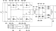
- FIG. 1 is a block diagram of a resonance conversion device according to an embodiment of the present invention.
- the resonance conversion device 100 includes an input filter circuit 101 , a full-bridge LLC converter circuit 102 , a transformer circuit 103 , a rectifier filter circuit 104 , and a controller 105 .
- the input filter circuit 101 receives a DC input voltage and filters the DC input voltage to output a filtered DC voltage.
- the full-bridge LLC converter circuit 102 is a resonance switch converter, and includes a resonance tank formed by a resonance inductor, a resonance capacitor, and an excitation inductor.
- the full-bridge LLC converter circuit 102 receives the filtered DC voltage, and outputs a converted voltage through the resonance tank formed by the resonance inductor, the resonance capacitor, and the excitation inductor.
- the specific implementation of the full-bridge LLC converter circuit 102 will be described in detail in the following embodiments.
- the transformer circuit 103 includes a primary side and a secondary side.
- the primary side of the transformer circuit 103 is coupled to the full-bridge LLC converter circuit to receive the converted voltage output by the resonance tank.
- the secondary side of the transformer circuit 103 induces the converted voltage to generate an induced voltage.
- the rectifier filter circuit 104 is coupled to the secondary side of the transformer circuit 103 to receive the induced voltage generated by the secondary side of the transformer circuit 103 .
- the rectifier filter circuit 104 rectifies and filters the induced voltage to output a DC output voltage as an output of the resonance conversion device 100 .
- the controller 105 is coupled to the full-bridge LLC converter circuit 102 and an output end of the rectifier filter circuit 104 .
- the controller 105 detects the DC output voltage output by the rectifier filter circuit 104 and receives a voltage command from outside.
- the voltage command includes an indication voltage used for indicating a value of the DC output voltage of the resonance conversion device 100 .
- the controller 105 further receives a load condition.
- the indication voltages include 5 V, 9 V, 15 V, 20 V, 28 V, 36 V, and 48 V.
- the indication voltage may satisfy the PD 3.1 specification (USB Power Delivery Specification Revision 3.1, Version 1.0) of the universal serial bus.
- the controller 105 controls the full-bridge LLC converter circuit 102 based on the voltage command and the value of the detected DC output voltage output by the rectifier filter circuit 104 .
- FIG. 9 is a control flow chart of the resonance conversion device according to an embodiment of the present invention.
- the controller 105 based on the indication voltage of the voltage command received from outside and the value of the detected DC output voltage output by the rectifier filter circuit 104 , the controller 105 sends a control signal to the full-bridge LLC converter circuit 102 to make the rectifier filter circuit 104 of the resonance conversion device 100 output a DC output voltage corresponding to the indication voltage.
- the controller 105 detects the DC output voltage output by the rectifier filter circuit 104 and receives a voltage command from outside.
- step S 902 the controller 105 determines whether an indication voltage of the voltage command is less than or equal to a threshold value.
- the controller 105 controls the full-bridge LLC converter circuit 102 into a half-bridge operation mode, and regulates the DC output voltage by performing half-bridge burst mode control on the full-bridge LLC converter circuit 102 based on the value of the DC output voltage output by the rectifier filter circuit 104 and detected by the controller 105 .
- the controller 105 regulates the DC output voltage by performing full-bridge burst mode control on the full-bridge LLC converter circuit 102 based on the value of the DC output voltage output by the rectifier filter circuit 104 and detected by the controller 105 .
- FIG. 12 is a control flow chart of the resonance conversion device according to an embodiment of the present invention. Refer to FIG. 1 and FIG. 12 together. Each step shown in FIG. 12 is performed by the controller 105 . In some embodiments of the present invention, based on the indication voltage of the voltage command received from outside, the load condition, and the value of the detected DC output voltage output by the rectifier filter circuit 104 , the controller 105 sends a control signal to the full-bridge LLC converter circuit 102 to make the rectifier filter circuit 104 of the resonance conversion device 100 output a DC output voltage corresponding to the indication voltage.
- step S 1201 the controller 105 detects the DC output voltage output by the rectifier filter circuit 104 , receives a load condition, and receives a voltage command from outside.
- step S 1202 the controller 105 determines whether an indication voltage of the voltage command is less than or equal to a threshold value. When the indication voltage is less than or equal to the threshold value, the controller 105 controls the full-bridge LLC converter circuit 102 into a half-bridge operation mode, and regulates the DC output voltage by performing half-bridge burst-variable frequency switching mode control on the full-bridge LLC converter circuit 102 based on the value of the DC output voltage output by the rectifier filter circuit 104 and detected by the controller 105 .
- the controller 105 regulates the DC output voltage by performing full-bridge burst-variable frequency switching mode control on the full-bridge LLC converter circuit 102 based on the value of the DC output voltage output by the rectifier filter circuit 104 and detected by the controller 105 .
- a first end 1021 of the first switch Q 1 is coupled to a first end 1011 of the input filter circuit 101 .
- the first switch Q 1 is connected in parallel to a diode D Q1 and a capacitor C Q1 .
- a first end 1022 of the second switch Q 2 is coupled to the first end 1021 of the first switch Q 1 and the first end 1011 of the input filter circuit 101 .
- the second switch Q 2 is connected in parallel to a diode D Q2 and a capacitor C Q2 .
- a first end 1023 of the third switch Q 3 is coupled to a second end 1027 of the first switch Q 1 , and a second end 1029 of the third switch Q 3 is coupled to a second end 1012 of the input filter circuit 101 .
- the third switch Q 3 is connected in parallel to a diode D Q3 and a capacitor C Q3 .
- a first end 1024 of the fourth switch Q 4 is coupled to a second end 1028 of the second switch Q 2 , and a second end 1030 of the fourth switch Q 4 is coupled to the second end 1029 of the third switch Q 3 .
- the fourth switch Q 4 is connected in parallel to a diode D Q4 and a capacitor C Q4 .
- the series branch includes a first resonance inductor L r , a second resonance inductor L m , and a resonance capacitor C r connected in series.
- the first resonance inductor L r is a resonance inductor of the full-bridge LLC converter circuit 102
- the second resonance inductor L m is an excitation inductor of the full-bridge LLC converter circuit 102
- the resonance capacitor C r is a resonance capacitor of the full-bridge LLC converter circuit 102 .
- the first resonance inductor L r , the second resonance inductor L m , and the resonance capacitor C r form a resonance tank of the full-bridge LLC converter circuit 102 .
- a first end 1025 of the series branch is coupled between the second end 1027 of the first switch Q 1 and the first end 1023 of the third switch Q 3 .
- a second end 1026 of the series branch is coupled between the second end 1028 of the second switch Q 2 and the first end 1024 of the fourth switch Q 4 .
- the primary side of the transformer circuit 103 includes a primary coil L 1 .
- the secondary side of the transformer circuit 103 includes a secondary coil L 2 .
- the ratio of the number of turns of the primary coil L 1 to the secondary coil L 2 is N 1 :N 2 .
- the second resonance inductor L m is connected in parallel to the primary coil L 1 of the primary side of the transformer circuit 103 .
- the secondary coil L 2 includes a first end 1031 and a second end 1032 , and the rectifier filter circuit 104 is coupled to the secondary side of the transformer circuit 103 through the first end 1031 and the second end 1032 of the secondary coil L 2 .
- the resonance conversion device 100 includes a load detection circuit 109 .
- the load detection circuit 109 is coupled to an output end of the rectifier filter circuit 104 to detect a DC output voltage and a load current of the rectifier filter circuit 104 .
- the load detection circuit 109 obtains the load condition by the DC output voltage and the load current of the rectifier filter circuit 104 .
- the rectifier filter circuit 104 includes a first forward conduction element D 1 , a second forward conduction element D 2 , a third forward conduction element D 3 , a fourth forward conduction element D 4 , and a capacitor C out .
- the first forward conduction element D 1 , the second forward conduction element D 2 , the third forward conduction element D 3 , and the fourth forward conduction element D 4 are all diodes.
- a first end 1091 of the first forward conduction element D 1 and a second end 1099 of the third forward conduction element D 3 are coupled.
- the first end 1031 of the secondary coil L 2 of the secondary side of the transformer circuit 103 is coupled between the first end 1091 of the first forward conduction element D 1 and the second end 1099 of the third forward conduction element D 3 .
- a first end 1092 of the second forward conduction element D 2 and a second end 10910 of the fourth forward conduction element D 4 are coupled.
- the second end 1032 of the secondary coil L 2 of the secondary side of the transformer circuit 103 is coupled between the first end 1092 of the second forward conduction element D 2 and the second end 10910 of the fourth forward conduction element D 4 .
- a second end 1097 of the first forward conduction element D 1 , a second end 1098 of the second forward conduction element D 2 , and a first end 1095 of the capacitor C out are coupled to each other.
- a first end 1093 of the third forward conduction element D 3 , a first end 1094 of the fourth forward conduction element D 4 , and a second end 1096 of the capacitor C out are coupled to each other.
- a voltage across the capacitor C out serves as the DC output voltage of the rectifier filter circuit 104 .
- a DC output voltage V o of the resonance conversion device 100 is the DC output voltage of the rectifier filter circuit 104 .
- the controller 105 includes a processor 107 , an analog-to-digital converter circuit 106 , and a digital-to-analog converter circuit 108 .
- the analog-to-digital converter circuit 106 of the controller 105 receives the load condition of the load detection circuit 109 , digitizes the load condition, and then transmits the digitized load condition to the processor 107 .
- the analog-to-digital converter circuit 106 also receives the DC output voltage output by the rectifier filter circuit 104 , digitizes the DC output voltage output by the rectifier filter circuit 104 , and then transmits the digitized DC output voltage to the processor 107 .
- the processor 107 receives a voltage command from outside, and the processor 107 obtains an indication voltage from the received voltage command.
- the indication voltage is used to indicate a value of the DC output voltage of the resonance conversion device 100 .
- FIG. 2 - 2 is a circuit structure diagram of the resonance conversion device according to another embodiment of the present invention.
- the rectifier filter circuit 104 in the resonance conversion device 100 shown in FIG. 2 - 2 includes a fifth switch Q 5 , a sixth switch Q 6 , a seventh switch Q 7 , an eighth switch Q 8 , and a capacitor C out .
- the fifth switch Q 5 , the sixth switch Q 6 , the seventh switch Q 7 , and the eighth switch Q 8 are all n-type MOS field effect transistors.
- a second end 2091 of the fifth switch Q 5 is coupled to a first end 2099 of the seventh switch Q 7 .
- the first end 1031 of the secondary coil L 2 of the secondary side of the transformer circuit 103 is coupled between the second end 2091 of the fifth switch Q 5 and the first end 2099 of the seventh switch Q 7 .
- a second end 2092 of the sixth switch Q 6 is coupled to a first end 20910 of the eighth switch Q 8 .
- the second end 1032 of the secondary coil L 2 of the secondary side of the transformer circuit 103 is coupled between the second end 2092 of the sixth switch Q 6 and the first end 20910 of the eighth switch Q 8 .
- a first end 2097 of the fifth switch Q 5 , a first end 2098 of the sixth switch Q 6 , and a first end 1095 of the capacitor C out are coupled to each other.
- a second end 2093 of the seventh switch Q 7 , a second end 2094 of the eighth switch Q 8 , and a second end 1096 of the capacitor C out are coupled to each other.
- a voltage across the capacitor C out serves as the DC output voltage of the rectifier filter circuit 104 .
- a DC output voltage V o of the resonance conversion device 100 is the DC output voltage of the rectifier filter circuit 104 .
- the controller 105 sends appropriate control signals to the fifth switch Q 5 , the sixth switch Q 6 , the seventh switch Q 7 , and the eighth switch Q 8 , to rectify the induced voltage.
- the controller 105 sends appropriate control signals to the fifth switch Q 5 , the sixth switch Q 6 , the seventh switch Q 7 , and the eighth switch Q 8 , so that the fifth switch Q 5 , the sixth switch Q 6 , the seventh switch Q 7 , and the eighth switch Q 8 behave the same as those of the first forward conduction element D 1 , the second forward conduction element D 2 , the third forward conduction element D 3 , and the fourth forward conduction element D 4 in FIG. 2 - 1 .
- FIG. 3 - 1 is a circuit structure diagram of the resonance conversion device according to another embodiment of the present invention.
- the primary side of the transformer circuit 103 in the resonance conversion device 100 shown in FIG. 3 - 1 includes the primary coil L 1 .
- the secondary side of the transformer circuit 103 includes a secondary coil L 3 .
- the secondary coil L 3 includes a first end 1033 , a second end 1034 , and a center tap junction 1035 .
- the rectifier filter circuit 104 is coupled to the secondary side of the transformer circuit 103 through the first end 1033 , the second end 1034 , and the center tap junction 1035 of the secondary coil L 3 .
- the rectifier filter circuit 104 includes a first forward conduction element D 5 , a second forward conduction element D 6 , and a capacitor C out .
- a second end 10913 of the first forward conduction element D 5 is coupled to the first end 1033 of the secondary coil L 3
- a second end 10914 of the second forward conduction element D 6 is coupled to the second end 1034 of the secondary coil L 3 .
- a first end 10912 of the second forward conduction element D 6 is coupled to a second end 10916 of the capacitor C out
- a first end 10911 of the first forward conduction element D 5 is coupled between the first end 10912 of the second forward conduction element D 6 and the second end 10916 of the capacitor C out .
- a first end 10915 of the capacitor C out is coupled to the center tap junction 1035 .
- a voltage across the capacitor C out serves as the DC output voltage of the rectifier filter circuit 104 .
- a DC output voltage V o of the resonance conversion device 100 is the DC output voltage of the rectifier filter circuit 104 .
- FIG. 3 - 2 is a circuit structure diagram of the resonance conversion device according to an embodiment of the present invention.
- the rectifier filter circuit 104 in the resonance conversion device 100 shown in FIG. 3 - 2 includes a fifth switch Q 9 , a sixth switch Q 10 , and a capacitor C out .
- a first end 20913 of the fifth switch Q 9 is coupled to a first end 1033 of the secondary coil L 3 .
- a first end 20914 of the sixth switch Q 10 is coupled to the second end 1034 of the secondary coil L 3
- a second end 20912 of the sixth switch Q 10 is coupled to a second end 10916 of the capacitor C out .
- a second end 20911 of the fifth switch is coupled between the second end 20912 of the sixth switch Q 10 and the second end 10916 of the capacitor C out .
- a first end 10915 of the capacitor C out is coupled to the center tap junction 1035 .
- a voltage across the capacitor C out serves as the DC output voltage of the rectifier filter circuit 104 .
- a DC output voltage V o of the resonance conversion device 100 is the DC output voltage of the rectifier filter circuit 104 .
- the controller 105 sends appropriate control signals to the fifth switch Q 9 and the sixth switch Q 10 , to rectify the induced voltage.
- the controller 105 sends appropriate control signals to the fifth switch Q 9 and the sixth switch Q 10 , so that the fifth switch Q 9 and the sixth switch Q 10 behave the same as those of the first forward conduction element D 5 and the second forward conduction element D 6 shown in FIG. 3 - 1 .
- the full-bridge LLC converter circuit 102 has two operation modes. One is that the controller 105 simultaneously controls the first switch Q 1 , the second switch Q 2 , the third switch Q 3 , and the fourth switch Q 4 to regulate the DC output voltage. This operation mode is referred to as a full-bridge operation mode. The other is that the controller 105 controls the second switch Q 2 to be turned off and controls the fourth switch Q 4 to be turned on. In this case, the second switch Q 2 acts as an open circuit, the fourth switch Q 4 acts as a short circuit, and the controller 105 controls only the first switch Q 1 and the third switch Q 3 to regulate the output DC voltage. This operation mode is referred to as a half-bridge operation mode.
- FIG. 4 is an equivalent circuit diagram of a series branch in a full-bridge LLC converter circuit according to an embodiment of the present invention. Referring to FIG. 2 - 1 and FIG. 4 together, s in FIG. 4 is the Laplace operator, and a gain of the resonance tank of the full-bridge LLC converter circuit 102 is
- R a ⁇ c 8 ⁇ 2 ⁇ N 1 2 N 2 2 ⁇
- R o is an output impedance looking out from the capacitor C out ,
- f r 1 2 ⁇ ⁇ ⁇ L r ⁇ C r is a resonance frequency
- f s is a switching frequency
- FIG. 5 is a response diagram of a product of a switching gain and a resonance tank gain and a normalized frequency according to an embodiment of the present invention.
- the switching gain*resonance tank gain is 1 at the resonance frequency f r .
- the switching gain*resonance tank gain is 0.5 at the resonance frequency f r .
- the switching gain*resonance tank gain is less than 1 when the switching frequency f s is greater than the resonance frequency f r , and the switching gain*resonance tank gain decreases when the switching frequency f s increases.
- the full-bridge LLC converter circuit 102 operates in an interval where the switching frequency is greater than or equal to the resonance frequency f r .
- the processor 107 transmits, to the digital-to-analog converter circuit 108 , the control signals to be transmitted to the first switch Q 1 , the second switch Q 2 , the third switch Q 3 , and the fourth switch Q 4 of the full-bridge LLC converter circuit 102 .
- the digital-to-analog converter circuit 108 converts the received control signals into appropriate drive signals, and then transmits the drive signals to the first switch Q 1 , the second switch Q 2 , the third switch Q 3 , and the fourth switch Q 4 of the full-bridge LLC converter circuit 102 , to drive the first switch Q 1 , the second switch Q 2 , the third switch Q 3 , and the fourth switch Q 4 .
- FIG. 6 is a timing diagram of a switch control signal according to an embodiment of the present invention.
- FIG. 7 is a timing diagram of a switch control signal according to an embodiment of the present invention.
- FIG. 10 is a control flow chart according to an embodiment of the present invention.
- FIG. 11 is a control flow chart according to an embodiment of the present invention. Refer to FIG. 2 - 1 , FIG. 6 , FIG. 7 , FIG. 10 , and FIG. 11 together. V GSQ1 recorded in FIG.
- V GSQ2 represents a voltage between a gate and a source of the second switch Q 2
- V GSQ3 represents a voltage between a gate and a source of the third switch Q 3
- V GSQ4 represents a voltage between a gate and a source of the fourth switch Q 4 .
- step S 903 further includes step S 1001 and step S 1002 .
- step S 1001 in response to the indication voltage being less than or equal to a threshold value, the processor 107 makes the digital-to-analog converter circuit 108 transmit the drive signals of V GSQ2 and V GSQ4 recorded in FIG. 6 , to control the voltage between the gate and the source of the second switch Q 2 and the voltage between the gate and the source of the fourth switch Q 4 , to turn off the second switch Q 2 and turn on the fourth switch Q 4 .
- the full-bridge LLC converter circuit 102 enters the half-bridge operation mode.
- step S 1002 the controller 105 detects the DC output voltage of the rectifier filter circuit 104 .
- the processor 107 makes the digital-to-analog converter circuit 108 transmit the drive signals having signal waveforms of V GSQ1 and V GSQ3 before a time point T 1 as recorded in FIG. 6 , to control the voltage between the gate and the source of the first switch Q 1 and the voltage between the gate and the source of the third switch Q 3 , thereby turning off the first switch Q 1 and the third switch Q 3 .
- the processor 107 makes the digital-to-analog converter circuit 108 transmit a first signal (a signal waveform of V GSQ1 from the time point T 1 to the time point T 2 as recorded in FIG. 6 ) to drive the first switch Q 1 , and transmit a second signal (a signal waveform of V GSQ3 from the time point T 1 to the time point T 2 as recorded in FIG. 6 ) to drive the third switch Q 3 , as shown from the time point T 1 to a time point T 2 recorded in FIG. 6 .
- the first signal and the second signal are periodic pulse signals in which a duty cycle is 50% and a frequency is a burst mode frequency, and the first signal and the second signal are complementary.
- the burst mode frequency is
- T r is a cycle of the first signal and the second signal.
- the processor 107 makes the digital-to-analog converter circuit 108 transmit drive signals having signal waveforms of V GSQ1 and V GSQ3 from the time point T 2 to a time point T 3 as recorded in FIG. 6 , to control the voltage between the gate and the source of the first switch Q 1 and the voltage between the gate and the source of the third switch Q 3 , to turn off the first switch Q 1 and the third switch Q 3 .
- the first preset voltage is greater than the indication voltage
- the second preset voltage is less than the indication voltage
- the controller 105 controls the DC output voltage to be within a range of the first preset voltage and the second preset voltage. Actual values of the first preset voltage and the second preset voltage are set according to design specifications.
- step S 1003 the controller 105 continues performing step S 1002 until the processor 107 receives a stop signal.
- step S 904 further includes step S 1101 and step S 1102 .
- the controller 105 detects the DC output voltage of the rectifier filter circuit 104 .
- the processor 107 makes the digital-to-analog converter circuit 108 transmit drive signals having signal waveforms of V GSQ1 , V GSQ2 , V GSQ3 , and V GSQ4 before the time point T 1 as recorded in FIG.
- the processor 107 makes the digital-to-analog converter circuit 108 transmit a first signal (a signal waveform of V GSQ1 from the time point T 4 to the time point T 5 as recorded in FIG. 7 ) to drive the first switch Q 1 and the fourth switch Q 4 , and transmit a second signal (a signal waveform of V GSQ2 from the time point T 4 to the time point T 5 as recorded in FIG. 7 ) to drive the second switch Q 2 and the third switch Q 3 , as shown from a time point T 4 to a time point T 5 recorded in FIG. 7 .
- the first signal and the second signal are periodic pulse signals in which a duty cycle is 50% and a frequency is a burst mode frequency, and the first signal and the second signal are complementary.
- the burst mode frequency is
- T r is a cycle of the first signal and the second signal.
- the burst mode frequency is selected as the resonance frequency
- f r 1 2 ⁇ ⁇ ⁇ L r ⁇ C r of the full-bridge LLC converter circuit 102 .
- the threshold value is half of a designed maximum output voltage of the resonance conversion device 100 at an operation point at the resonance frequency
- f r 1 2 ⁇ ⁇ ⁇ L r ⁇ C r is designed to be 50 V, and the threshold value is selected to be 25 V.
- FIG. 8 is a timing diagram of a switch control signal according to an embodiment of the present invention.
- the first switch Q 1 and the third switch Q 3 are simultaneously turned on or the second switch Q 2 and the fourth switch Q 4 are simultaneously turned on, a large current may be generated to damage the first switch Q 1 and the third switch Q 3 or the second switch Q 2 and the fourth switch Q 4 . Therefore, the first signal (the signal waveform of V GSQ1 from the time point T 1 to the time point T 2 as recorded in FIG. 6 ) and the second signal (the signal waveform of V GSQ3 from the time point T 1 to the time point T 2 as recorded in FIG.
- a dead time is set from a time point T 7 to a time point T 8 (corresponding to a time point T 13 to a time point T 14 ), from a time point T 9 to a time point T 10 (corresponding to a time point T 15 to a time point T 16 ), from a time point T 10 to a time point T 11 (corresponding to a time point T 16 to a time point TO, and from a time point T 12 to the time point T 13 .
- the duty cycle of the first signal and the second signal without the dead time is 50%.
- the processor 107 makes the digital-to-analog converter circuit 108 transmit the first signal (the signal waveform of V GSQ1 from the time point T 1 to the time point T 2 as recorded in FIG. 6 ) to drive the first switch Q 1 , and transmit the second signal (the signal waveform of V GSQ3 from the time point T 1 to the time point T 2 as recorded in FIG. 6 ) to drive the third switch Q 3 , as shown from the time point T 1 to the time point T 2 recorded in FIG. 6 .
- the first signal and the second signal are periodic pulse signals in which a duty cycle is 50% and a frequency is a burst mode frequency, and the first signal and the second signal are complementary.
- the burst mode frequency is
- T r is a cycle of the first signal and the second signal.
- the processor 107 makes the digital-to-analog converter circuit 108 transmit drive signals having signal waveforms of V GSQ1 and V GSQ3 from the time point T 2 to a time point T 3 as recorded in FIG. 6 , to control the voltage between the gate and the source of the first switch Q 1 and the voltage between the gate and the source of the third switch Q 3 , to turn off the first switch Q 1 and the third switch Q 3 .
- step S 1402 the controller 105 continues performing step S 1401 until the processor 107 receives a stop signal.
- FIG. 15 is a control flow chart according to an embodiment of the present invention.
- the foregoing step S 1305 further includes steps S 1403 to S 1407 .
- the processor 107 makes the digital-to-analog converter circuit 108 transmit a third signal to drive the first switch Q 1 and transmit a fourth signal to drive the third switch Q 3 .
- the third signal and the fourth signal are variable frequency periodic pulse signals having a duty cycle of 50%, and the third signal and the fourth signal are complementary.
- step S 1403 the processor 107 determines whether the difference between the DC output voltage and the preset voltage is greater than 0. If the difference between the DC output voltage and the preset voltage is greater than 0, step S 1404 is performed.
- step S 1404 the processor 107 increases a frequency of the third signal and a frequency of the fourth signal. If the difference between the DC output voltage and the preset voltage is less than 0, step S 1405 is performed. In step S 1405 , the processor 107 decreases the frequency of the third signal and the frequency of the fourth signal. If the difference between the DC output voltage and the preset voltage is 0, the frequency of the third signal and the frequency of the fourth signal are not changed.
- step S 1406 the processor 107 makes the digital-to-analog converter circuit 108 transmit the third signal to drive the first switch Q 1 and transmit the fourth signal to drive the third switch Q 3 .
- step S 1407 the controller 105 continues performing the foregoing steps S 1403 to S 1406 until the processor 107 receives a stop signal.
- FIG. 16 is a control flow chart according to an embodiment of the present invention. Referring to FIG. 7 and FIG. 16 together, as shown in FIG. 16 , the foregoing step S 1204 further includes steps S 1501 to S 1504 .
- step S 1501 the processor 107 determines whether the indication voltage of the voltage command is in a second voltage interval. If the processor 107 determines that the indication voltage of the voltage command is not in the second voltage interval, step S 1503 is performed. If the processor 107 determines that the indication voltage of the voltage command is in the second voltage interval, step S 1502 is performed. In step S 1502 , whether the load condition is light is further determined, if yes, step S 1503 is performed, and if not, step S 1504 is performed.
- step S 1503 the processor 107 regulates the DC output voltage by performing full-bridge burst mode control on the full-bridge LLC converter circuit 102 based on the DC output voltage.
- step S 1504 the DC output voltage is regulated by performing full-bridge variable frequency control on the full-bridge LLC converter circuit 102 based on the difference between the DC output voltage and the indication voltage.
- FIG. 17 is a control flow chart according to an embodiment of the present invention. As shown in FIG. 17 , step S 1503 further includes step S 1601 and step S 1602 . Because step S 1601 is the same as the foregoing step S 1101 , and step S 1602 is the same as the foregoing step S 1102 , the description is not repeated here.
- FIG. 18 is a control flow chart according to an embodiment of the present invention.
- the foregoing step S 1504 further includes steps S 1603 to S 1607 .
- the processor 107 makes the digital-to-analog converter circuit 108 transmit a third signal to drive the first switch Q 1 and the fourth switch Q 4 and transmit a fourth signal to drive the second switch Q 2 and the third switch Q 3 .
- the third signal and the fourth signal are variable frequency periodic pulse signals having a duty cycle of 50%, and the third signal and the fourth signal are complementary.
- the processor 107 determines whether the difference between the DC output voltage and the preset voltage is greater than 0. If the difference between the DC output voltage and the preset voltage is greater than 0, step S 1604 is performed.
- step S 1604 the processor 107 increases the frequency of the third signal and the frequency of the fourth signal. If the difference between the DC output voltage and the preset voltage is less than 0, step S 1605 is performed. In step S 1605 , the processor 107 decreases the frequency of the third signal and the frequency of the fourth signal. If the difference between the DC output voltage and the preset voltage is 0, the frequency of the third signal and the frequency of the fourth signal are not changed.
- step S 1606 the processor 107 makes the digital-to-analog converter circuit 108 transmit the third signal to drive the first switch Q 1 and the fourth switch Q 4 and transmit the fourth signal to drive the second switch Q 2 and the third switch Q 3 .
- step S 1607 the controller 105 continues performing the foregoing steps S 1603 to S 1606 until the processor 107 receives a stop signal.
- the burst mode frequency is selected as the resonance frequency
- the burst mode frequency includes the resonance frequency of the resonance conversion device. In some embodiments of the present invention, the burst mode frequency includes the resonance frequency
- f r 1 2 ⁇ ⁇ ⁇ L r ⁇ C r of the full-bridge LLC converter circuit 102 .
- the second voltage interval is an interval including the maximum output voltage of the resonance conversion device 100 at the operation point at the resonance frequency
- the first voltage interval is an interval including the threshold value.
- the maximum output voltage of the resonance conversion device 100 at the operation point at the resonance frequency f r is designed to be 50 V and the threshold value is selected to be 25 V
- the second voltage interval ranges from 48 to 50 V
- the first voltage interval ranges from 24 to 25 V.
- FIG. 19 is a block diagram of a universal serial bus (USB) circuit and an external device according to an embodiment of the present invention.
- the universal serial bus circuit 1900 includes a resonance conversion device 1901 .
- the resonance conversion device 1901 may be the resonance conversion device 100 described in any of the foregoing embodiments.
- the universal serial bus circuit 1900 is connected to the external device 1902 .
- the universal serial bus circuit 1900 sends a voltage command to the resonance conversion device 1901 according to a requirement of the external device 1902 , so that the resonance conversion device 1901 provides a fixed voltage to the external device 1902 .
- FIG. 20 is an efficiency comparison diagram of the resonance conversion device at light load.
- FIG. 21 is an efficiency comparison diagram of the resonance conversion device at heavy load. Refer to FIG. 20 and FIG. 21 together.
- the efficiency of using the half-bridge burst mode control is better than that of using the full-bridge burst mode control below 25 V.
- the efficiency of using the full-bridge burst mode control is better than that of using the conventional full-bridge phase-shift mode control.
- the efficiency of using the half-bridge burst mode control is better than that of using the full-bridge burst mode control below 25 V.
- the efficiency of using the full-bridge burst mode control is better than that of using the conventional full-bridge phase-shift mode control.
- the results shown in FIG. 20 and FIG. 21 may verify that the control method of the resonance conversion device shown in FIG. 9 has good efficiency.
- FIG. 22 is an efficiency comparison diagram of half-bridge burst mode control and half-bridge variable frequency control of the resonance conversion device.
- FIG. 23 is an efficiency comparison diagram of full-bridge burst mode control and full-bridge variable frequency control of the resonance conversion device. Refer to FIG. 22 and FIG. 23 together.
- the efficiency of using the half-bridge burst mode control is better than that of using the half-bridge variable frequency control when the load is below 40%, and the efficiency of using the half-bridge variable frequency control is better than that of using the half-bridge burst mode control when the load is above 40%.
- the efficiency of using the full-bridge burst mode control is better than that of using the full-bridge variable frequency control when the load is below 30%, and the efficiency of using the full-bridge variable frequency control is better than that of using the full-bridge burst mode control when the load is above 30%.
- the results shown in FIG. 22 and FIG. 23 may verify that the control method of the resonance conversion device shown in FIG. 12 has good efficiency.
- some embodiments of the present invention can avoid efficiency reduction by a single-stage design. Some embodiments of the present invention can achieve a wide output voltage and improve the efficiency by switching the operation mode and control method of the full-bridge LLC converter circuit based on the indication voltage. Some embodiments of the present invention can further improve the efficiency by controlling using a variable frequency control method within a specific voltage and load range.
Landscapes
- Engineering & Computer Science (AREA)
- Power Engineering (AREA)
- Dc-Dc Converters (AREA)
- Control Of Motors That Do Not Use Commutators (AREA)
- Input Circuits Of Receivers And Coupling Of Receivers And Audio Equipment (AREA)
Abstract
Description
where
is a quality factor,
is a reflective load resistance, Ro is an output impedance looking out from the capacitor Cout,
is a normalized switching frequency,
is a resonance frequency, fs is a switching frequency, and
conversion gain=switching gain*resonance tank gain*ratio of number of turns of the primary coil L 1 to the secondary coil L 2(N 2 /N 1).
and Tr is a cycle of the first signal and the second signal. When the
and Tr is a cycle of the first signal and the second signal.
In some embodiments of the present invention, the burst mode frequency includes the resonance frequency of the resonance conversion device. In some embodiments of the present invention, the burst mode frequency includes the resonance frequency
of the full-bridge
For example, in order to cover the foregoing indication voltages 5 V, 9 V, 15 V, 20 V, 28 V, 36 V, and 48 V, the maximum output voltage of the
is designed to be 50 V, and the threshold value is selected to be 25 V.
and Tr is a cycle of the first signal and the second signal. When the
In some embodiments of the present invention, the burst mode frequency includes the resonance frequency of the resonance conversion device. In some embodiments of the present invention, the burst mode frequency includes the resonance frequency
of the full-bridge
and the first voltage interval is an interval including the threshold value. In the embodiment in which the maximum output voltage of the
Claims (44)
Applications Claiming Priority (2)
| Application Number | Priority Date | Filing Date | Title |
|---|---|---|---|
| TW111103015A TWI805201B (en) | 2022-01-24 | 2022-01-24 | Resonant converter device and universal serial bus circuit |
| TW111103015 | 2022-01-24 |
Publications (2)
| Publication Number | Publication Date |
|---|---|
| US20230238890A1 US20230238890A1 (en) | 2023-07-27 |
| US12040720B2 true US12040720B2 (en) | 2024-07-16 |
Family
ID=87314747
Family Applications (1)
| Application Number | Title | Priority Date | Filing Date |
|---|---|---|---|
| US17/704,442 Active 2043-03-21 US12040720B2 (en) | 2022-01-24 | 2022-03-25 | Resonance conversion device and universal serial bus circuit |
Country Status (3)
| Country | Link |
|---|---|
| US (1) | US12040720B2 (en) |
| CN (1) | CN116526851A (en) |
| TW (1) | TWI805201B (en) |
Families Citing this family (1)
| Publication number | Priority date | Publication date | Assignee | Title |
|---|---|---|---|---|
| CN119134925B (en) * | 2024-11-11 | 2025-02-28 | 泉州师范学院 | LLC resonant converter for automotive DC-DC converters |
Citations (17)
| Publication number | Priority date | Publication date | Assignee | Title |
|---|---|---|---|---|
| US6804129B2 (en) | 1999-07-22 | 2004-10-12 | 02 Micro International Limited | High-efficiency adaptive DC/AC converter |
| US20060133119A1 (en) | 2004-12-21 | 2006-06-22 | Fujio Nomura | Electric power unit |
| TW201027892A (en) | 2009-01-05 | 2010-07-16 | Spi Electronic Co Ltd | Resonant converter with phase-shift output line |
| US20150049515A1 (en) * | 2013-08-13 | 2015-02-19 | Delphi Technologies, Inc. | Resonant converter and method of operating the same |
| CN104467443A (en) | 2015-01-06 | 2015-03-25 | 山东鲁能智能技术有限公司 | Super-wide output voltage range charger based on LLC topology and control method |
| US20150098254A1 (en) | 2013-10-09 | 2015-04-09 | Power Systems Technologies Ltd. | Controller for use with a power converter and method of operating the same |
| US20150162840A1 (en) | 2010-02-18 | 2015-06-11 | Arda Power Inc | Dc-dc converter circuit using an llc circuit in the region of voltage gain above unity |
| US20150229225A1 (en) | 2014-02-12 | 2015-08-13 | Delta Electronics, Inc. | Resonant converters and control methods thereof |
| US9263960B2 (en) | 2013-09-16 | 2016-02-16 | Delta Electronics, Inc. | Power converters for wide input or output voltage range and control methods thereof |
| CN108258910A (en) | 2017-12-25 | 2018-07-06 | 浙江大学 | A kind of full-bridge LLC resonant transform circuits and its wide range output control method |
| CN108964466A (en) | 2017-05-19 | 2018-12-07 | 恩智浦有限公司 | Power source converter and method for operating power source converter |
| US20190068069A1 (en) * | 2017-08-31 | 2019-02-28 | Google Inc. | Programmable Power Adapter |
| US10389233B1 (en) | 2018-10-08 | 2019-08-20 | Infineon Technologies Austria Ag | Switched mode power supply with PFC burst mode control |
| TW201937329A (en) | 2018-02-23 | 2019-09-16 | 台達電子工業股份有限公司 | Power supply device and control method thereof |
| CN110504847A (en) | 2018-05-18 | 2019-11-26 | 龙海特尔福汽车电子研究所有限公司 | A kind of AC-DC converter based on PFC+LLC topology |
| US20230077388A1 (en) * | 2021-08-20 | 2023-03-16 | Delta Electronics (Thailand) Public Co., Ltd. | On-the-fly topology morphing for frequency-multiplier half-bridge operation |
| US20230198371A1 (en) * | 2020-09-30 | 2023-06-22 | Guangdong Oppo Mobile Telecommunications Corp., Ltd. | Power source providing apparatus, and charging method and system |
Family Cites Families (5)
| Publication number | Priority date | Publication date | Assignee | Title |
|---|---|---|---|---|
| CN104953837B (en) * | 2014-03-31 | 2018-05-08 | 台达电子企业管理(上海)有限公司 | Control device and control method and Switching Power Supply for power inverter |
| US20200220368A1 (en) * | 2019-01-08 | 2020-07-09 | Google Llc | Universal Adapter |
| KR102739582B1 (en) * | 2019-08-02 | 2024-12-09 | 삼성전자주식회사 | Display apparatus |
| WO2021168831A1 (en) * | 2020-02-28 | 2021-09-02 | Astec International Limited | Power measurements in switched mode power supplies |
| CN113765398A (en) * | 2021-09-10 | 2021-12-07 | 安徽工业大学 | A novel bidirectional LLC resonant converter topology and control method suitable for energy storage systems |
-
2022
- 2022-01-24 TW TW111103015A patent/TWI805201B/en active
- 2022-02-21 CN CN202210156467.XA patent/CN116526851A/en active Pending
- 2022-03-25 US US17/704,442 patent/US12040720B2/en active Active
Patent Citations (17)
| Publication number | Priority date | Publication date | Assignee | Title |
|---|---|---|---|---|
| US6804129B2 (en) | 1999-07-22 | 2004-10-12 | 02 Micro International Limited | High-efficiency adaptive DC/AC converter |
| US20060133119A1 (en) | 2004-12-21 | 2006-06-22 | Fujio Nomura | Electric power unit |
| TW201027892A (en) | 2009-01-05 | 2010-07-16 | Spi Electronic Co Ltd | Resonant converter with phase-shift output line |
| US20150162840A1 (en) | 2010-02-18 | 2015-06-11 | Arda Power Inc | Dc-dc converter circuit using an llc circuit in the region of voltage gain above unity |
| US20150049515A1 (en) * | 2013-08-13 | 2015-02-19 | Delphi Technologies, Inc. | Resonant converter and method of operating the same |
| US9263960B2 (en) | 2013-09-16 | 2016-02-16 | Delta Electronics, Inc. | Power converters for wide input or output voltage range and control methods thereof |
| US20150098254A1 (en) | 2013-10-09 | 2015-04-09 | Power Systems Technologies Ltd. | Controller for use with a power converter and method of operating the same |
| US20150229225A1 (en) | 2014-02-12 | 2015-08-13 | Delta Electronics, Inc. | Resonant converters and control methods thereof |
| CN104467443A (en) | 2015-01-06 | 2015-03-25 | 山东鲁能智能技术有限公司 | Super-wide output voltage range charger based on LLC topology and control method |
| CN108964466A (en) | 2017-05-19 | 2018-12-07 | 恩智浦有限公司 | Power source converter and method for operating power source converter |
| US20190068069A1 (en) * | 2017-08-31 | 2019-02-28 | Google Inc. | Programmable Power Adapter |
| CN108258910A (en) | 2017-12-25 | 2018-07-06 | 浙江大学 | A kind of full-bridge LLC resonant transform circuits and its wide range output control method |
| TW201937329A (en) | 2018-02-23 | 2019-09-16 | 台達電子工業股份有限公司 | Power supply device and control method thereof |
| CN110504847A (en) | 2018-05-18 | 2019-11-26 | 龙海特尔福汽车电子研究所有限公司 | A kind of AC-DC converter based on PFC+LLC topology |
| US10389233B1 (en) | 2018-10-08 | 2019-08-20 | Infineon Technologies Austria Ag | Switched mode power supply with PFC burst mode control |
| US20230198371A1 (en) * | 2020-09-30 | 2023-06-22 | Guangdong Oppo Mobile Telecommunications Corp., Ltd. | Power source providing apparatus, and charging method and system |
| US20230077388A1 (en) * | 2021-08-20 | 2023-03-16 | Delta Electronics (Thailand) Public Co., Ltd. | On-the-fly topology morphing for frequency-multiplier half-bridge operation |
Also Published As
| Publication number | Publication date |
|---|---|
| TW202332180A (en) | 2023-08-01 |
| US20230238890A1 (en) | 2023-07-27 |
| CN116526851A (en) | 2023-08-01 |
| TWI805201B (en) | 2023-06-11 |
Similar Documents
| Publication | Publication Date | Title |
|---|---|---|
| US9209697B2 (en) | Switching power-supply device | |
| US8536851B2 (en) | Quasi-resonant systems and methods with multi-mode control | |
| US7843708B2 (en) | Synchronous rectifier type series resonant converter for operating in intermittence mode | |
| CN101582638B (en) | Switching power source apparatus | |
| US11664736B2 (en) | Auto-tuned synchronous rectifier controller | |
| US8488338B2 (en) | Controller with valley switching and limited maximum frequency for quasi-resonant power converters | |
| EP0765022B1 (en) | Uninterrupted switching regulator | |
| JP2002300779A (en) | Switching power supply | |
| CN111654189B (en) | Resonant power conversion device | |
| US20130271876A1 (en) | Switching control circuit and switching power supply apparatus | |
| JP5424031B2 (en) | Power factor correction circuit | |
| US9093918B2 (en) | Control circuit for offline power converter without input capacitor | |
| US12040720B2 (en) | Resonance conversion device and universal serial bus circuit | |
| WO2023065230A1 (en) | Hold-up time circuit for llc converter | |
| JP6919612B2 (en) | Non-contact power supply device | |
| US7729136B2 (en) | Isolated DC-DC converter | |
| US12155312B2 (en) | Power converter controller, power converter and method for operating control of a power stage based on an intermediate voltage with respect to a threshold value determined from a turns ratio of a transformer | |
| CN118282217A (en) | Asymmetric half-bridge flyback converter and control circuit and control method thereof | |
| TWI809716B (en) | Asymmetric half-bridge converter | |
| TW202122901A (en) | Dynamic multi-function power controller to provide a protection mechanism in response to different peak load requirements, avoid the continuous high wattage state when the abnormal state is not resolved | |
| JP2002354798A (en) | Switching power supply | |
| US9276481B2 (en) | Power control device for dynamically adjusting frequency | |
| KR100359709B1 (en) | Switching mode power supply | |
| JP6791744B2 (en) | Switching power supply | |
| JPS59226656A (en) | Switching power source |
Legal Events
| Date | Code | Title | Description |
|---|---|---|---|
| AS | Assignment |
Owner name: NATIONAL TAIPEI UNIVERSITY OF TECHNOLOGY, TAIWAN Free format text: ASSIGNMENT OF ASSIGNORS INTEREST;ASSIGNORS:LAI, YEN-SHIN;HUANG, YONG-YI;WU, XIANG-YU;AND OTHERS;REEL/FRAME:059403/0207 Effective date: 20220323 Owner name: CHICONY POWER TECHNOLOGY CO., LTD., TAIWAN Free format text: ASSIGNMENT OF ASSIGNORS INTEREST;ASSIGNORS:LAI, YEN-SHIN;HUANG, YONG-YI;WU, XIANG-YU;AND OTHERS;REEL/FRAME:059403/0207 Effective date: 20220323 |
|
| FEPP | Fee payment procedure |
Free format text: ENTITY STATUS SET TO UNDISCOUNTED (ORIGINAL EVENT CODE: BIG.); ENTITY STATUS OF PATENT OWNER: LARGE ENTITY |
|
| STPP | Information on status: patent application and granting procedure in general |
Free format text: DOCKETED NEW CASE - READY FOR EXAMINATION |
|
| STPP | Information on status: patent application and granting procedure in general |
Free format text: NOTICE OF ALLOWANCE MAILED -- APPLICATION RECEIVED IN OFFICE OF PUBLICATIONS |
|
| STPP | Information on status: patent application and granting procedure in general |
Free format text: PUBLICATIONS -- ISSUE FEE PAYMENT RECEIVED |
|
| STPP | Information on status: patent application and granting procedure in general |
Free format text: PUBLICATIONS -- ISSUE FEE PAYMENT VERIFIED |
|
| STCF | Information on status: patent grant |
Free format text: PATENTED CASE |