US12035546B2 - Method for producing an electronic component which includes a self-assembled monolayer - Google Patents
Method for producing an electronic component which includes a self-assembled monolayer Download PDFInfo
- Publication number
- US12035546B2 US12035546B2 US17/251,669 US201917251669A US12035546B2 US 12035546 B2 US12035546 B2 US 12035546B2 US 201917251669 A US201917251669 A US 201917251669A US 12035546 B2 US12035546 B2 US 12035546B2
- Authority
- US
- United States
- Prior art keywords
- denotes
- atoms
- denote
- compounds
- formula
- Prior art date
- Legal status (The legal status is an assumption and is not a legal conclusion. Google has not performed a legal analysis and makes no representation as to the accuracy of the status listed.)
- Active, expires
Links
Images


Classifications
-
- H—ELECTRICITY
- H10—SEMICONDUCTOR DEVICES; ELECTRIC SOLID-STATE DEVICES NOT OTHERWISE PROVIDED FOR
- H10K—ORGANIC ELECTRIC SOLID-STATE DEVICES
- H10K71/00—Manufacture or treatment specially adapted for the organic devices covered by this subclass
- H10K71/10—Deposition of organic active material
-
- G—PHYSICS
- G11—INFORMATION STORAGE
- G11C—STATIC STORES
- G11C13/00—Digital stores characterised by the use of storage elements not covered by groups G11C11/00, G11C23/00, or G11C25/00
- G11C13/0002—Digital stores characterised by the use of storage elements not covered by groups G11C11/00, G11C23/00, or G11C25/00 using resistive RAM [RRAM] elements
- G11C13/0009—RRAM elements whose operation depends upon chemical change
- G11C13/0014—RRAM elements whose operation depends upon chemical change comprising cells based on organic memory material
- G11C13/0016—RRAM elements whose operation depends upon chemical change comprising cells based on organic memory material comprising polymers
-
- H—ELECTRICITY
- H10—SEMICONDUCTOR DEVICES; ELECTRIC SOLID-STATE DEVICES NOT OTHERWISE PROVIDED FOR
- H10K—ORGANIC ELECTRIC SOLID-STATE DEVICES
- H10K10/00—Organic devices specially adapted for rectifying, amplifying, oscillating or switching; Organic capacitors or resistors having potential barriers
- H10K10/50—Bistable switching devices
-
- H—ELECTRICITY
- H10—SEMICONDUCTOR DEVICES; ELECTRIC SOLID-STATE DEVICES NOT OTHERWISE PROVIDED FOR
- H10K—ORGANIC ELECTRIC SOLID-STATE DEVICES
- H10K10/00—Organic devices specially adapted for rectifying, amplifying, oscillating or switching; Organic capacitors or resistors having potential barriers
- H10K10/701—Organic molecular electronic devices
-
- H—ELECTRICITY
- H10—SEMICONDUCTOR DEVICES; ELECTRIC SOLID-STATE DEVICES NOT OTHERWISE PROVIDED FOR
- H10K—ORGANIC ELECTRIC SOLID-STATE DEVICES
- H10K19/00—Integrated devices, or assemblies of multiple devices, comprising at least one organic element specially adapted for rectifying, amplifying, oscillating or switching, covered by group H10K10/00
- H10K19/202—Integrated devices comprising a common active layer
-
- H—ELECTRICITY
- H10—SEMICONDUCTOR DEVICES; ELECTRIC SOLID-STATE DEVICES NOT OTHERWISE PROVIDED FOR
- H10K—ORGANIC ELECTRIC SOLID-STATE DEVICES
- H10K30/00—Organic devices sensitive to infrared radiation, light, electromagnetic radiation of shorter wavelength or corpuscular radiation
- H10K30/671—Organic radiation-sensitive molecular electronic devices
-
- H—ELECTRICITY
- H10—SEMICONDUCTOR DEVICES; ELECTRIC SOLID-STATE DEVICES NOT OTHERWISE PROVIDED FOR
- H10K—ORGANIC ELECTRIC SOLID-STATE DEVICES
- H10K71/00—Manufacture or treatment specially adapted for the organic devices covered by this subclass
- H10K71/10—Deposition of organic active material
- H10K71/12—Deposition of organic active material using liquid deposition, e.g. spin coating
-
- H—ELECTRICITY
- H10—SEMICONDUCTOR DEVICES; ELECTRIC SOLID-STATE DEVICES NOT OTHERWISE PROVIDED FOR
- H10K—ORGANIC ELECTRIC SOLID-STATE DEVICES
- H10K71/00—Manufacture or treatment specially adapted for the organic devices covered by this subclass
- H10K71/10—Deposition of organic active material
- H10K71/16—Deposition of organic active material using physical vapour deposition [PVD], e.g. vacuum deposition or sputtering
-
- H—ELECTRICITY
- H10—SEMICONDUCTOR DEVICES; ELECTRIC SOLID-STATE DEVICES NOT OTHERWISE PROVIDED FOR
- H10K—ORGANIC ELECTRIC SOLID-STATE DEVICES
- H10K71/00—Manufacture or treatment specially adapted for the organic devices covered by this subclass
- H10K71/40—Thermal treatment, e.g. annealing in the presence of a solvent vapour
-
- H—ELECTRICITY
- H10—SEMICONDUCTOR DEVICES; ELECTRIC SOLID-STATE DEVICES NOT OTHERWISE PROVIDED FOR
- H10K—ORGANIC ELECTRIC SOLID-STATE DEVICES
- H10K85/00—Organic materials used in the body or electrodes of devices covered by this subclass
- H10K85/60—Organic compounds having low molecular weight
- H10K85/649—Aromatic compounds comprising a hetero atom
- H10K85/657—Polycyclic condensed heteroaromatic hydrocarbons
- H10K85/6574—Polycyclic condensed heteroaromatic hydrocarbons comprising only oxygen in the heteroaromatic polycondensed ring system, e.g. cumarine dyes
-
- H—ELECTRICITY
- H10—SEMICONDUCTOR DEVICES; ELECTRIC SOLID-STATE DEVICES NOT OTHERWISE PROVIDED FOR
- H10K—ORGANIC ELECTRIC SOLID-STATE DEVICES
- H10K85/00—Organic materials used in the body or electrodes of devices covered by this subclass
- H10K85/60—Organic compounds having low molecular weight
- H10K85/649—Aromatic compounds comprising a hetero atom
- H10K85/657—Polycyclic condensed heteroaromatic hydrocarbons
- H10K85/6576—Polycyclic condensed heteroaromatic hydrocarbons comprising only sulfur in the heteroaromatic polycondensed ring system, e.g. benzothiophene
Definitions
- the invention relates to a process for the production of an electronic component comprising a self-assembled monolayer (SAM) using mesogenic compounds containing a spacer group and an anchor group, where the anchor group is an ester derivative of secondary or tertiary alcohols; the present invention furthermore relates to the use of the components in electronic switching elements and to compounds for the production of the SAM.
- SAM self-assembled monolayer
- DRAM dynamic random access memory
- memristor is a contraction of the words “memory” and “resistor” and denotes a component which is able to change its electrical resistance reproducibly between high and low electrical resistance. The respective state (high resistance or low resistance) is retained even without a supply voltage, meaning that non-volatile memories can be achieved with memristors.
- mesogenic compounds are known from the prior art and are compounds which contain one or more mesogenic groups.
- a mesogenic group is the part of a molecule which, due to the anisotropy of its attractive and repulsive interactions, makes a significant contribution to low-molecular-weight substances forming a liquid-crystalline (LC) mesophase (C. Tschierske, G. Pelzl, S. Diele, Angew. Chem. 2004, 116, 6340-6368).
- LC liquid-crystalline
- the invention furthermore relates to the use of the component according to the invention in a memristive electronic switching element.
- mesogenic group is known to the person skilled in the art and is defined in accordance with C. Tschierske, G. Pelzl, S. Diele, Angew. Chem. 2004, 116, 6340-6368, as the part of a molecule or macromolecule which, due to the anisotropy of its attracting and repelling interactions, makes a significant contribution to the low-molecular-weight or polymeric substances forming a liquid-crystalline mesophase.
- the majority of mesogenic groups consist of rigid rod- or disc-shaped units.
- Particularly preferred groups Sp′ are, for example, in each case straight-chain ethylene, propylene, butylene, pentylene, hexylene, heptylene, octylene, nonylene, decylene, undecylene, dodecylene, octadecylene, perfluoroethylene, perfluoropropylene, perfluorobutylene, perfluoropentylene, perfluorohexylene, perfluoroheptylene, perfluorooctylene, perfluorononylene, perfluorodecylene, perfluoroundecylene, perfluorododecylene, perfluorooctadecylene, ethylenoxyethylene, methylenoxybutylene, ethylenethioethylene, ethylene-N-methyliminoethylene, 1-methylalkylene, ethenylene, propenylene and butenylene.
- Suitable substrates are known to the person skilled in the art. Particularly suitable substrates are selected from:
- the application of the solution of the material to the substrate can be carried out by conventional methods for the coating of surfaces, such as dip coating, knife coating, spray coating, roller coating, spin coating, furthermore spray coating, slot-die coating, and conventional printing processes, such as, for example, ink-jet printing, screen printing, microcontact stamp printing, and in addition by deposition from the gas phase. Spin coating and deposition from the gas phase are preferred.
- Sulfonic acid esters of the formula I are prepared via the acid chloride by reaction with an alcohol in the presence of a base, for example triethylamine, as described, for example, in Z. Guan, X. Chai, S. Yu, Q. Meng, Q. Wu, Chem. Biol. Drug Des. 2010, 76, 496-504.
- a base for example triethylamine
- Another process, in particular for the preparation of secondary alkyl sulphonates, is, according to I. Galyker, W. C. Still, Tetrahedron Lett. 1982, 23, 4461-4464, the Mitsunobu condensation.
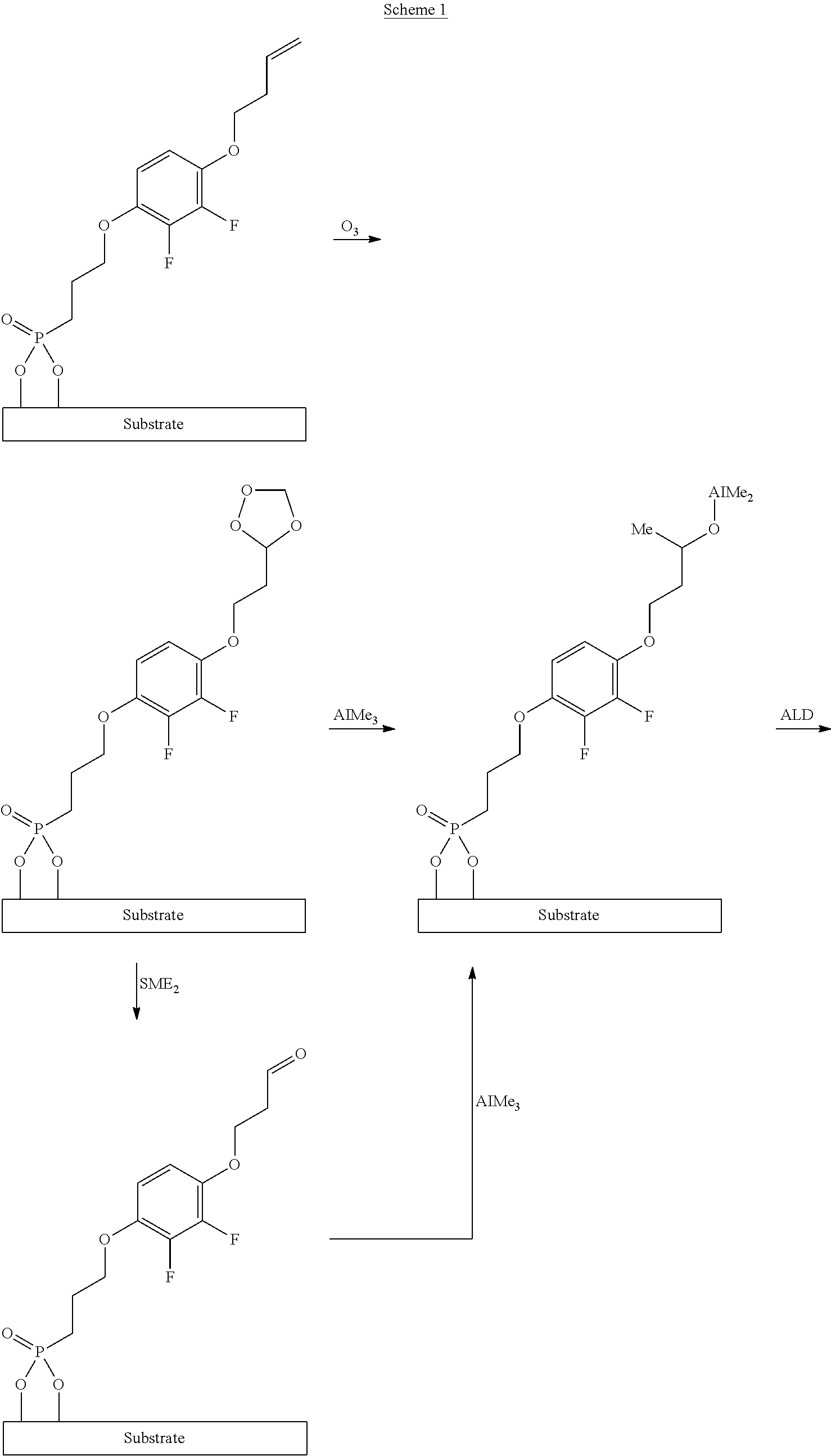
- a 1-2 nm thick aluminium oxide layer is produced on a silicon wafer (8 ⁇ 8 mm, p ++ -doped) by means of atomic layer deposition.
- the substrate is subsequently degreased three times with acetone in an ultrasound bath at room temperature and then cleaned in an oxygen plasma ( ⁇ 0.3 mbar of O 2 , 2 min, 100 W).
- a 5 mM solution of the compound di-tert-butyl (3-(2,3-difluoro-4-(4-pentylcyclohexyl)phenoxy)propyl)phosphonate (Synthesis Example 1) in decalin is applied to the substrate prepared in this way by spin coating at 4000 rpm for 30 s.
- the substrate is subsequently annealed at 110° C. for 1 h, washed with isopropanol and dried under nitrogen.
- the contact angle of water on the substrate is determined after each of the following steps:
- the value of 106° measured after completion of the production process indicates the presence of a stable monolayer.
- the component is characterised electrically as described in WO2018/007337 A1 on pages 72 to 75 and exhibits memristive switching behaviour.
- the contact angle of water on the substrate is determined after each of the following steps:
- Wafer (substrate) before treatment 90°
- Substrate after degreasing 73°
- plasma treatment 7°
- spin coating 71°
- drying 102°.
- the value of 102° measured after completion of the production process indicates the presence of a stable monolayer.
- a glass substrate (8 ⁇ 8 mm) is degreased three times with isopropanol in an ultrasound bath at room temperature and then cleaned for 10 min with a freshly prepared mixture of conc. sulfuric acid and 30 percent hydrogen peroxide (3:1, “piranha solution”), washed with water and dried under nitrogen.
- a 0.1 mM solution of the compound di-tert-butyl (3-(2,3-difluoro-4-(4-pentylcyclohexyl)phenoxy)propyl)phosphonate (Synthesis Example 1) in decalin is applied to the substrate prepared in this way by spin coating at 4000 rpm for 30 s.
- the substrate is subsequently annealed at 110° C. for 1 h, washed with tetrahydrofuran and dried under nitrogen.
- the value of 63° measured after completion of the production process indicates the presence of a stable monolayer.
- a 1-2 nm thick aluminium oxide layer is produced on a silicon wafer (8 ⁇ 8 mm, p ++ -doped) by means of atomic layer deposition.
- the substrate is subsequently degreased three times with acetone in an ultrasound bath at room temperature and then cleaned in an oxygen plasma ( ⁇ 0.3 mbar of O 2 , 1 min, 200 W).
- a 1 mM solution of the compound di-tert-butyl (11-(2,3-difluoro-4-(4-pentylcyclohexyl)phenoxy)undecyl)phosphonate in tetrahydrofuran is applied to the substrate prepared in this way by spin coating (application of 4 ml of solution over the course of 10 s with rotation at 150 rpm, subsequently at 3000 rpm for 35 s).
- the substrate is subsequently annealed at 160° C. for 1 h, washed with 10 ml of tetrahydrofuran and dried under nitrogen.
- the component is characterised electrically with a mercury electrode as counterelectrode as described in WO2018/007337 A1 on pages 72 to 75 and exhibits memristive switching behaviour.
- the current/voltage curve is shown in FIG. 1 .
- a substrate, produced as in Example 4, is derivatised with the free phosphonic acid corresponding to the ester from Example 4 (11-(2,3-difluoro-4-(4-pentylcyclohexyl)phenoxy)undecyl)phosphonic acid, substance example 19 from WO2018/007337 A2) by dip coating.
- the substrate is dipped into a 1 mM solution of this phosphonic acid in tetrahydrofuran for 72 h, subsequently dried in a stream of nitrogen, dried at 120° C. under nitrogen for 1 h, rinsed with 10 ml of tetrahydrofuran and dried again in a stream of nitrogen.
- the component is characterised electrically in the same way as the component from Example 4.
- the current/voltage curve is shown in FIG. 2 .
Landscapes
- Physics & Mathematics (AREA)
- Engineering & Computer Science (AREA)
- Spectroscopy & Molecular Physics (AREA)
- Manufacturing & Machinery (AREA)
- Chemical & Material Sciences (AREA)
- Materials Engineering (AREA)
- Electromagnetism (AREA)
- Organic Low-Molecular-Weight Compounds And Preparation Thereof (AREA)
- Semiconductor Memories (AREA)
- Organic Chemistry (AREA)
- Health & Medical Sciences (AREA)
- Life Sciences & Earth Sciences (AREA)
- Biochemistry (AREA)
- General Health & Medical Sciences (AREA)
- Molecular Biology (AREA)
- Thin Film Transistor (AREA)
- Electroluminescent Light Sources (AREA)
Abstract
Description
-
- (1) provision of a substrate having a substrate surface,
- (2) application of a solution comprising one or more compounds of the formula I to the substrate surface,
- (3) heating of the substrate to a temperature in the range from 60° C. to 300° C.,
- where formula I is defined as follows:
R1-(A1-Z1)r—(B1)n—(Z2-A2)s-Sp-G (I) - in which
- R1 denotes H, an alkyl or alkoxy radical having 1 to 15 C atoms, where, in addition, one or more CH2 groups in these radicals may each be replaced, independently of one another, by —C≡C—, —CH═CH—,

-
- —O—, —S—, —CF2O—, —OCF2—, —CO—O—, —O—CO—, —SiR0R00—, —NH—, —NR0— or —SO2— in such a way that O atoms are not linked directly to one another, and in which, in addition, one or more H atoms may be replaced by halogen, CN, SCN or SF5,
- R0, R00 denote, identically or differently, an alkyl or alkoxy radical having 1 to 15 C atoms, in which, in addition, one or more H atoms may be replaced by halogen,
- A1, A2 on each occurrence, identically or differently, denote an aromatic, heteroaromatic, alicyclic or heteroaliphatic ring having 4 to 25 ring atoms, which may also contain condensed rings and which may be mono- or polysubstituted by Y,
- Y on each occurrence, identically or differently, denotes F, Cl, CN, SCN, SF5 or straight-chain or branched, in each case optionally fluorinated, alkyl, alkoxy, alkylcarbonyl, alkoxycarbonyl, alkylcarbonyloxy or alkoxycarbonyloxy having 1 to 12 C atoms,
- B1 denotes


-
-
- where the groups may be oriented in both directions,
- L1 to L5, independently of one another, denote F, Cl, Br, I, CN, SF5, CF3 or OCF3, preferably Cl or F, where L3 may alternatively also denote H,
- Z1, Z2 on each occurrence, identically or differently, denote a single bond, —CF2O—, —OCF2—, —CF2S—, —SCF2—, —CH2O—, —OCH2—, —C(O)O—, —OC(O)—, —C(O)S—, —SC(O)—, —CH2—, —(CH2)2—, —(CH2)3, —(CH2)4—, —CF2—, —CF2—CF2—, —CF2—CH2—, —CH2—CF2—, —CH═CH—, —CF═CF—, —CF═CH—, —CH═CF—, —(CH2)3O—, —O(CH2)3—, —C≡C—, —O—, —S—, —C═N—, —N═C—, —N═N—, —N═N(O)—, —N(O)═N— or —N═C—C═N—,
- Sp denotes a spacer group or a single bond,
- G denotes-SO2ORV, —OP(O)(ORV)2, —PO(ORV)2, —C(OH)(PO(ORV)2)2, —COORV or —Si(ORV)3,
- RV denotes secondary or tertiary alkyl having 3 to 20 C atoms,
- r and s, independently of one another, denote 0, 1, 2 or 3,
- where r+s 4, and
- n denotes 0 or 1.
-
R1-(A1-Z1)r—B1—(Z2-A2)s-Sp-G (IA)
in which the groups and parameters occurring have the meanings indicated above.
-
- A1 and A2, independently of one another and identically or differently on each occurrence, are particularly preferably selected from the following groups:
- a) 1,4-phenylene, in which, in addition, one or two CH groups may be replaced by N and in which, in addition, one or more H atoms may be replaced by Y,
- b) the group consisting of trans-1,4-cyclohexylene and 1,4-cyclohexenylene, in which, in addition, one or more non-adjacent CH2 groups may be replaced by —O— and/or —S— and in which, in addition, one or more H atoms may be replaced by Y, and
- c) the group consisting of 1,3-dioxolane-2,4-diyl, tetrahydrofuran-2,5-diyl, cyclobutane-1,3-diyl, 1,4-bicyclo[2.2.2]octanediyl, piperidine-1,5-diyl and thiophene-2,5-diyl, in which, in addition, one or more H atoms may be replaced by Y,
- where Y has the meaning indicated above under formula I and preferably denotes F, CI, CN or CF3.
- A1 and A2, independently of one another and identically or differently on each occurrence, are particularly preferably selected from the following groups:
-
- Sp′ denotes straight-chain or branched alkylene having 1 to 20, preferably 1 to 12 C atoms, which is optionally mono- or poly-substituted by F, Cl, Br, I or CN and in which, in addition, one or more non-adjacent CH2 groups may each be replaced, independently of one another, by —O—, —S—, —NH—, —NR0—, —SiR00R000—, —CO—, —COO—, —OCO—, —OCO—O—, —S—CO—, —CO—S—, —NR00—CO—O—, —O—CO—NR00—, —NR00—CO—NR00—, —CH═CH— or —C≡C— in such a way that O and/or S atoms are not linked directly to one another,
- X′ denotes —O—, —S—, —CO—, —COO—, —OCO—, —O—COO—, —CO—NR00—, —NR00—CO—, —NR00—CO—NR00—, —OCH2—, —CH2O—, —SCH2—, —CH2S—, —CF2O—, —OCF2—, —CF2S—, —SCF2—, —CF2CH2—, —CH2CF2—, —CF2CF2—, —CH═N—, —N═CH—, —N═N—, —CH═CR00—, —CYx═CYx′—, —C≡C—, —CH═CH—COO—, —OCO—CH═CH— or a single bond,
- R00
- and R000 each, independently of one another, denote H or alkyl having 1 to 12 C atoms, and
- Yx and Yx′ each, independently of one another, denote H, F, Cl or CN.
- X′ is preferably —O—, —S—, —CO—, —COO—, —OCO—, —O—COO—, —CO—NR0—, —NR0—CO—, —NR0—CO—NR0— or a single bond.
| R1-B1-Sp-G | IAa | ||
| R1-(A1-Z1)-B1-Sp-G | IAb | ||
| R1-(A1-Z1)2-B1-Sp-G | IAc | ||
| R1-B1-(Z2-A2)-Sp-G | IAd | ||
| R1-B1-(Z2-A2)2-Sp-G | IAe | ||
| R1-(A1-Z1)-B1-(Z2-A2-)-Sp-G | IAf | ||
-
- in which R1, A1, A2, B1, Z1, Z2, Sp and G have the meanings indicated above and preferably
- A1 and denote

-
- B1 denotes

-
-
- where the groups may be oriented in both directions,
- R1 denotes alkyl having 1-15 C atoms, preferably having 1-7 C atoms, in particular CH3, C2H5, n-C3H7, n-C4H9, n-C5H11, n-C6H13 or n-C7H15.
- L1 and L2, independently of one another, denote Cl or F,
- L3 denotes F,
- Y1 and Y2, independently of one another, denote H, Cl or F,
- Z1, Z2, independently of one another, denote a single bond, —CF2O—, —OCF2—, —CH2O—, OCH2— or —CH2CH2—,
- Sp denotes unbranched 1,ω-alkylene having 1 to 12 C atoms,
- G denotes —CH═CH2, —OH, —SH, —SO2OH, —OP(O)(OH)2, —PO(OH)2, —COH(PO(OH)2)2, —COOH, —Si(OR)3 or —SiCl3.
-
-
- Sp denotes unbranched 1,ω-perfluoroalkylene having 1 to 12 C atoms,
- where R1, A1, A2, B1, Z1, Z2 and G have the meanings indicated above.
R2-G Ig,
in which R2 has the meaning indicated for R1 above under formula I and G has the meaning indicated above under formula I.
CH3(CH2)r-G Ig-1
CF3(CF2)sCH2CH2-G Ig-2
-
- in which
- G denotes —PO(ORV)2 or —SO2ORV,
- RV denotes secondary or tertiary alkyl having 3 to 20 C atoms,
- r denotes an integer from 1 to 20,
- s denotes an integer from 1 to 18, and
- t denotes an integer from 1 to 4.


-
- in which R1 and G have the meanings given above and preferably
- R1 denotes alkyl having 1 to 7 C atoms,
- G denotes —SO2ORV or —PO(ORV)2,
- RV denotes an isopropyl or tert-butyl radical, and
- v denotes an integer from 1 to 12, preferably from 2 to 7.

-
- (1) provision of a substrate having a substrate surface,
- (2) application of a solution comprising one or more compounds of the formula IB onto the substrate surface,
- (3) heating of the substrate to a temperature in the range from 60° C. to 300° C.,
- (4) treatment of the surface with ozone,
- where formula IB is defined as follows:

-
- in which
- R3 and R4, independently of one another, denote H, F, CI, alkyl or alkoxy having 1 to 6 C atoms, preferably H or CH3, particularly preferably H,
- Sp′ denotes straight-chain or branched or cyclic alkylene having 1 to 20 C atoms, in which one or more H atoms may be replaced by F or CH3 and in which one or more non-adjacent CH2 groups may be replaced by 0, preferably straight-chain alkylene, preferably straight-chain alkylene having 1 to 15 C atoms, in particular having 2 to 10 C atoms, and in which the other groups and parameters have the meanings indicated for formula I in claim 1, with the proviso that the anchor group G is not vinyl.
-
- in which R3, R4 and Sp′ have the meanings indicated for formula IB.
-
- element semiconductors, such as Si, Ge, C (diamond, graphite, graphene, fullerene), α-Sn, B, Se and Te;
- compound semiconductors, preferably
- group III-V semiconductors, in particular GaAs, GaP, InP, InSb, InAs, GaSb, GaN, TaN, TiN, MoN, WN, AlN, InN, AlxGa1-xAs and InxGa1-xNi,
- group II-VI semiconductors, in particular ZnO, ZnS, ZnSe, ZnTe, CdS, CdSe, CdTe, Hg(1-x)Cd(x)Te, BeSe, BeTex and HgS;
- group III-VI semiconductors, in particular GaS, GaSe, GaTe, InS, InSex and InTe,
- group I-III-VI semiconductors, in particular CuInSe2, CuInGaSe2, CuInS2 and CuInGaS2,
- group IV-IV semiconductors, in particular SiC and SiGe,
- group IV-VI semiconductors, in particular SeTe;
- organic semiconductors, in particular polythiophene, tetracene, pentacene, phthalocyanines, PTCDA, MePTCDI, quinacridone, acridone, indanthrone, flaranthrone, perinone, AlQ3, and mixed systems, in particular PEDOT:PSS and polyvinylcarbazole/TLNQ complexes;
- metals, in particular Ta, Ti, Co, Mo, Pt, Ru, Au, Ag, Cu, Al, W and Mg;
- conductive oxidic materials, in particular indium tin oxide (ITO), indium gallium oxide (IGO), InGa-α-ZnO (IGZO), aluminium-doped zinc oxide (AZO), tin-doped zinc oxide (TZO), fluorine-doped tin oxide (FTO) and antimony tin oxide;
- metal oxides (SiO2, Al2O3, TiO2, HfO2 and ZrO2);
- metal nitrides (Si3N4, TaNx and TiNx); mixed metal oxynitrides (TiNxOy and TaNxOy).


| Wafer (substrate) before treatment: | 81° | ||
| Substrate after degreasing: | 72° | ||
| After plasma treatment: | 5° | ||
| After spin coating: | 81° | ||
| After drying: | 106°. | ||
| Wafer (substrate) before treatment: | 90° | ||
| Substrate after degreasing: | 73° | ||
| After plasma treatment: | 7° | ||
| After spin coating: | 71° | ||
| After drying: | 102°. | ||
| Glass substrate before treatment: | 35° | ||
| Substrate after degreasing: | 15° | ||
| After piranha treatment: | 7° | ||
| After spin coating: | 25° | ||
| After drying: | 63°. | ||
Claims (20)
R1-(A1-Z1)r—(B1)n—(Z2-A2)s-Sp-G (I)


R1-(A1-Z1)r—B1—(Z2-A2)s-Sp-G (IA)


R2-G Ig
CH3(CH2)r-G Ig-1
CF3(CF2)sCH2CH2-G Ig-2
R1-(A1-Z1)r—B1—(Z2-A2)s-Sp-G (IA)


Applications Claiming Priority (3)
| Application Number | Priority Date | Filing Date | Title |
|---|---|---|---|
| DE102018004733.5A DE102018004733A1 (en) | 2018-06-14 | 2018-06-14 | Method for producing an electronic component containing a self-organized monolayer |
| DE102018004733.5 | 2018-06-14 | ||
| PCT/EP2019/065160 WO2019238649A1 (en) | 2018-06-14 | 2019-06-11 | Method for producing an electronic component which includes a self-assembled monolayer |
Publications (2)
| Publication Number | Publication Date |
|---|---|
| US20210257569A1 US20210257569A1 (en) | 2021-08-19 |
| US12035546B2 true US12035546B2 (en) | 2024-07-09 |
Family
ID=67001741
Family Applications (1)
| Application Number | Title | Priority Date | Filing Date |
|---|---|---|---|
| US17/251,669 Active 2041-09-15 US12035546B2 (en) | 2018-06-14 | 2019-06-11 | Method for producing an electronic component which includes a self-assembled monolayer |
Country Status (10)
| Country | Link |
|---|---|
| US (1) | US12035546B2 (en) |
| EP (1) | EP3807880B1 (en) |
| JP (1) | JP7453922B2 (en) |
| KR (1) | KR102834025B1 (en) |
| CN (1) | CN112262434B (en) |
| DE (1) | DE102018004733A1 (en) |
| IL (1) | IL279380B2 (en) |
| SG (1) | SG11202012423XA (en) |
| TW (1) | TWI837138B (en) |
| WO (1) | WO2019238649A1 (en) |
Families Citing this family (9)
| Publication number | Priority date | Publication date | Assignee | Title |
|---|---|---|---|---|
| DE102017005884A1 (en) * | 2016-07-07 | 2018-01-11 | Merck Patent Gmbh | Electronic switching element |
| EP3813132A1 (en) | 2019-10-21 | 2021-04-28 | Merck Patent GmbH | Electronic switching device |
| US12163223B2 (en) | 2019-10-29 | 2024-12-10 | Merck Patent Gmbh | Process for the production of a molecular layer and electronic component comprising same |
| EP4102571B1 (en) | 2021-06-09 | 2024-11-13 | Merck Patent GmbH | Electronic element comprising a plurality of cells arranged in a three dimensional array of cells and method for producing such an electronic device |
| EP4174077A1 (en) | 2021-10-27 | 2023-05-03 | Merck Patent GmbH | Electronic switching device |
| TW202347336A (en) | 2022-03-16 | 2023-12-01 | 德商馬克專利公司 | Electronic switching device |
| IL300665B1 (en) | 2022-03-16 | 2026-04-01 | Merck Patent Gmbh | Electronic Switching Device |
| EP4349842A1 (en) | 2022-10-04 | 2024-04-10 | Merck Patent GmbH | Hydroxyaminophosphinic acid derivatives |
| JP2026500467A (en) * | 2022-11-11 | 2026-01-07 | メルク パテント ゲゼルシャフト ミット ベシュレンクテル ハフツング | Liquid crystal SAMs via spin-coating assembly and their area-selective deposition properties |
Citations (22)
| Publication number | Priority date | Publication date | Assignee | Title |
|---|---|---|---|---|
| EP0207890B1 (en) | 1985-06-11 | 1990-03-14 | Ciba-Geigy Ag | Microbicidal composition |
| US5189030A (en) | 1985-06-11 | 1993-02-23 | Ciba-Geigy Corporation | 1-amino-2-phenylethanephosphonic acids as microbiocides |
| WO1998028311A1 (en) | 1996-12-20 | 1998-07-02 | Symphar S.A. | Pharmaceutical aminophosphonic acid derivatives |
| JP2000192046A (en) | 1998-12-25 | 2000-07-11 | Canon Inc | Liquid crystal composition, liquid crystal element having the same, display device using the same, and display method |
| US20050099209A1 (en) | 2002-06-21 | 2005-05-12 | Luyken R. J. | Circuit element having a first layer composed of an electrically insulating substrate material, a method for producing a circuit element, bispyridinium compounds and their use in circuit elements |
| JP2007177051A (en) | 2005-12-27 | 2007-07-12 | Toyota Central Res & Dev Lab Inc | Organic inorganic hybrid composition |
| EP1879240A2 (en) | 2006-07-13 | 2008-01-16 | Hitachi, Ltd. | Field effect transistor, organic thin-film transistor and manufacturing method of organic transistor |
| US20090131384A1 (en) | 2006-03-22 | 2009-05-21 | Syndexa Pharmaceuticals Corporation | Compounds and methods for treatment of disorders associated with er stress |
| US20120184510A1 (en) | 2011-01-14 | 2012-07-19 | Colburn Raymond W | Cold menthol receptor-1 antagonists |
| WO2012127542A1 (en) | 2011-03-24 | 2012-09-27 | Kabushiki Kaisha Toshiba | Organic molecular memory and method of manufacturing the same |
| WO2013004372A1 (en) | 2011-07-07 | 2013-01-10 | Merck Patent Gmbh | Liquid-crystalline medium |
| WO2013043624A1 (en) | 2011-09-23 | 2013-03-28 | Merck Sharp & Dohme Corp. | Substituted pyrimidines |
| US20130129922A1 (en) * | 2011-11-21 | 2013-05-23 | Qualcomm Mems Technologies, Inc. | Batch processing for electromechanical systems and equipment for same |
| US20140008601A1 (en) | 2011-03-24 | 2014-01-09 | Kabushiki Kaisha Toshiba | Organic molecular memory |
| US20140009379A1 (en) * | 2012-07-06 | 2014-01-09 | Qualcomm Mems Technologies, Inc. | Cavity liners for electromechanical systems devices |
| US20140141564A1 (en) | 2012-11-20 | 2014-05-22 | Boe Technology Group Co., Ltd. | Method for surface treatment |
| WO2014169988A1 (en) | 2013-04-16 | 2014-10-23 | Merck Patent Gmbh | Device containing a liquid-crystalline medium |
| DE102015000120A1 (en) | 2015-01-07 | 2016-07-07 | Merck Patent Gmbh | Electronic component |
| US20160355405A1 (en) | 2015-06-02 | 2016-12-08 | Korea Advanced Institute Of Science And Technology | Method of fabricating array of nanoparticle clusters using thermal transformation of sublimable liquid crystal film |
| US20170298166A1 (en) | 2016-04-18 | 2017-10-19 | Coleen Pugh | Polybutadiene graft copolymers as coupling agents for carbon black and silica dispersion in rubber compounds |
| DE102017005884A1 (en) | 2016-07-07 | 2018-01-11 | Merck Patent Gmbh | Electronic switching element |
| EP3270664A1 (en) | 2015-03-11 | 2018-01-17 | Toray Industries, Inc. | Organic el display device and method for manufacturing same |
Family Cites Families (6)
| Publication number | Priority date | Publication date | Assignee | Title |
|---|---|---|---|---|
| DE10037391A1 (en) * | 2000-08-01 | 2002-02-14 | Covion Organic Semiconductors | Structurable materials, processes for their production and their use |
| JP4506105B2 (en) | 2003-06-10 | 2010-07-21 | Dic株式会社 | Liquid crystal alignment accelerator, liquid crystal composition and optical anisotropic body |
| US20080020148A1 (en) * | 2004-10-07 | 2008-01-24 | Markus Klein | Chromane Derivatives Method for Production and the Use Thereof |
| DE102007043921A1 (en) * | 2006-10-12 | 2008-04-17 | Merck Patent Gmbh | Polymerizable compounds useful for making liquid crystal displays of the polymer sustained alignment type comprise polymerizable groups bonded to a biaryl structure |
| EP3510122B1 (en) * | 2016-09-07 | 2020-12-16 | Merck Patent GmbH | Liquid-crystal media and light modulation element |
| CN106206944A (en) * | 2016-09-29 | 2016-12-07 | 南京大学 | A kind of nano-film memristor and preparation method thereof |
-
2018
- 2018-06-14 DE DE102018004733.5A patent/DE102018004733A1/en active Granted
-
2019
- 2019-06-11 WO PCT/EP2019/065160 patent/WO2019238649A1/en not_active Ceased
- 2019-06-11 EP EP19732550.9A patent/EP3807880B1/en active Active
- 2019-06-11 IL IL279380A patent/IL279380B2/en unknown
- 2019-06-11 KR KR1020217000579A patent/KR102834025B1/en active Active
- 2019-06-11 CN CN201980038244.XA patent/CN112262434B/en active Active
- 2019-06-11 JP JP2020569202A patent/JP7453922B2/en active Active
- 2019-06-11 US US17/251,669 patent/US12035546B2/en active Active
- 2019-06-11 SG SG11202012423XA patent/SG11202012423XA/en unknown
- 2019-06-13 TW TW108120512A patent/TWI837138B/en active
Patent Citations (33)
| Publication number | Priority date | Publication date | Assignee | Title |
|---|---|---|---|---|
| EP0207890B1 (en) | 1985-06-11 | 1990-03-14 | Ciba-Geigy Ag | Microbicidal composition |
| US5189030A (en) | 1985-06-11 | 1993-02-23 | Ciba-Geigy Corporation | 1-amino-2-phenylethanephosphonic acids as microbiocides |
| WO1998028311A1 (en) | 1996-12-20 | 1998-07-02 | Symphar S.A. | Pharmaceutical aminophosphonic acid derivatives |
| JP2000192046A (en) | 1998-12-25 | 2000-07-11 | Canon Inc | Liquid crystal composition, liquid crystal element having the same, display device using the same, and display method |
| US20050099209A1 (en) | 2002-06-21 | 2005-05-12 | Luyken R. J. | Circuit element having a first layer composed of an electrically insulating substrate material, a method for producing a circuit element, bispyridinium compounds and their use in circuit elements |
| JP2007177051A (en) | 2005-12-27 | 2007-07-12 | Toyota Central Res & Dev Lab Inc | Organic inorganic hybrid composition |
| US20090131384A1 (en) | 2006-03-22 | 2009-05-21 | Syndexa Pharmaceuticals Corporation | Compounds and methods for treatment of disorders associated with er stress |
| US20080012009A1 (en) | 2006-07-13 | 2008-01-17 | Tomihiro Hashizume | Field effect transistor, organic thin-film transistor and manufacturing method of organic transistor |
| EP1879240A2 (en) | 2006-07-13 | 2008-01-16 | Hitachi, Ltd. | Field effect transistor, organic thin-film transistor and manufacturing method of organic transistor |
| US20120184510A1 (en) | 2011-01-14 | 2012-07-19 | Colburn Raymond W | Cold menthol receptor-1 antagonists |
| US9172053B2 (en) | 2011-03-24 | 2015-10-27 | Kabushiki Kaisha Toshiba | Organic molecular memory and method of manufacturing the same |
| WO2012127542A1 (en) | 2011-03-24 | 2012-09-27 | Kabushiki Kaisha Toshiba | Organic molecular memory and method of manufacturing the same |
| US20140008601A1 (en) | 2011-03-24 | 2014-01-09 | Kabushiki Kaisha Toshiba | Organic molecular memory |
| WO2013004372A1 (en) | 2011-07-07 | 2013-01-10 | Merck Patent Gmbh | Liquid-crystalline medium |
| US9234136B2 (en) | 2011-07-07 | 2016-01-12 | Merck Patent Gmbh | Liquid-crystalline medium |
| WO2013043624A1 (en) | 2011-09-23 | 2013-03-28 | Merck Sharp & Dohme Corp. | Substituted pyrimidines |
| US9079930B2 (en) | 2011-09-23 | 2015-07-14 | Merck Sharp & Dohme Corp. | Substituted pyrimidines |
| US20130129922A1 (en) * | 2011-11-21 | 2013-05-23 | Qualcomm Mems Technologies, Inc. | Batch processing for electromechanical systems and equipment for same |
| US20140009379A1 (en) * | 2012-07-06 | 2014-01-09 | Qualcomm Mems Technologies, Inc. | Cavity liners for electromechanical systems devices |
| US20140141564A1 (en) | 2012-11-20 | 2014-05-22 | Boe Technology Group Co., Ltd. | Method for surface treatment |
| US20160060530A1 (en) | 2013-04-16 | 2016-03-03 | Merck Patent Gmbh | Device containing a liquid-crystalline medium |
| WO2014169988A1 (en) | 2013-04-16 | 2014-10-23 | Merck Patent Gmbh | Device containing a liquid-crystalline medium |
| US10741778B2 (en) | 2015-01-07 | 2020-08-11 | Merck Patent Gmbh | Electronic component including molecular layer |
| DE102015000120A1 (en) | 2015-01-07 | 2016-07-07 | Merck Patent Gmbh | Electronic component |
| US10896942B2 (en) | 2015-03-11 | 2021-01-19 | Toray Industries, Inc. | Organic EL display device and method for manufacturing same |
| EP3270664A1 (en) | 2015-03-11 | 2018-01-17 | Toray Industries, Inc. | Organic el display device and method for manufacturing same |
| US20160355405A1 (en) | 2015-06-02 | 2016-12-08 | Korea Advanced Institute Of Science And Technology | Method of fabricating array of nanoparticle clusters using thermal transformation of sublimable liquid crystal film |
| US20170298166A1 (en) | 2016-04-18 | 2017-10-19 | Coleen Pugh | Polybutadiene graft copolymers as coupling agents for carbon black and silica dispersion in rubber compounds |
| WO2018007337A2 (en) | 2016-07-07 | 2018-01-11 | Merck Patent Gmbh | Electronic switching element |
| US20190312216A1 (en) | 2016-07-07 | 2019-10-10 | Merck Patent Gmbh | Electronic switching element |
| TW201811718A (en) | 2016-07-07 | 2018-04-01 | 德商馬克專利公司 | Electronic switching element |
| DE102017005884A1 (en) | 2016-07-07 | 2018-01-11 | Merck Patent Gmbh | Electronic switching element |
| US11522141B2 (en) | 2016-07-07 | 2022-12-06 | Merck Patent Gmbh | Electronic switching element |
Non-Patent Citations (11)
| Title |
|---|
| English translation of Office action in corresponding ROC (Taiwan) Patent Application No. 108120512 (pp. 1-4). |
| International Search report PCT/EP2019/065160 dated Oct. 1, 2019 (pp. 1-3). |
| Liu et al., "Conductivity switching and memory effect in polymer brushes . . . " Synthetic Metals 2012, 162, 13, 1059-1064. |
| Machine translation of the written opinion (ETWOS) (Year: 0000). * |
| Office Action in corresponding Chinese Patent Application for Invention No. 201980038244.X dated Dec. 1, 2023 (pp. 1-14) and English translation thereof (pp. 1-13). |
| Office Action in corresponding German application 102018004733.5dated Dec. 12, 2021 (pp. 1-5). |
| Office Action in corresponding Singapore application 11202012423X dated Oct. 20, 2022 (pp. 1-2) and written Opinion pp. (1-6). |
| Queffélec et al., ‘Surface Modification Using Phosphonic Acids and Esters’, Chemical Reviews 2012, 112, 7, 3777-3807. |
| Schreiber: "Structure and growth of self-assembling monlayers" Progress in Surface Science 2000_65_5-8_ 151-256. |
| Wang et al., "Direct regioselective phosphonation . . . " Chemical Communications 2014, 50, 92, 14409-14411. |
| Yoon: "The rate of charge Tunneling . . . " J. Am. Chem. Soc. 136 (2014) 16-19. |
Also Published As
| Publication number | Publication date |
|---|---|
| DE102018004733A1 (en) | 2019-12-19 |
| IL279380A (en) | 2021-01-31 |
| IL279380B2 (en) | 2026-04-01 |
| JP2021527337A (en) | 2021-10-11 |
| CN112262434B (en) | 2024-09-20 |
| KR20210019071A (en) | 2021-02-19 |
| EP3807880B1 (en) | 2026-04-29 |
| JP7453922B2 (en) | 2024-03-21 |
| CN112262434A (en) | 2021-01-22 |
| TW202005975A (en) | 2020-02-01 |
| EP3807880A1 (en) | 2021-04-21 |
| IL279380B1 (en) | 2025-12-01 |
| TWI837138B (en) | 2024-04-01 |
| WO2019238649A1 (en) | 2019-12-19 |
| SG11202012423XA (en) | 2021-01-28 |
| US20210257569A1 (en) | 2021-08-19 |
| KR102834025B1 (en) | 2025-07-14 |
Similar Documents
| Publication | Publication Date | Title |
|---|---|---|
| US12035546B2 (en) | Method for producing an electronic component which includes a self-assembled monolayer | |
| US11522141B2 (en) | Electronic switching element | |
| US12336362B2 (en) | Diamondoid compounds | |
| US12193328B2 (en) | Aromatic compounds and use thereof for formation of molecular layers and fabrication of switching elements for memristive devices | |
| US12424277B2 (en) | Electronic switching device | |
| US12163223B2 (en) | Process for the production of a molecular layer and electronic component comprising same | |
| KR102954479B1 (en) | aromatic compounds | |
| KR102954480B1 (en) | diamond-type compounds | |
| JP2025533346A (en) | Hydroxyaminophosphinic acid derivatives |
Legal Events
| Date | Code | Title | Description |
|---|---|---|---|
| FEPP | Fee payment procedure |
Free format text: ENTITY STATUS SET TO UNDISCOUNTED (ORIGINAL EVENT CODE: BIG.); ENTITY STATUS OF PATENT OWNER: LARGE ENTITY |
|
| STPP | Information on status: patent application and granting procedure in general |
Free format text: APPLICATION DISPATCHED FROM PREEXAM, NOT YET DOCKETED |
|
| STPP | Information on status: patent application and granting procedure in general |
Free format text: DOCKETED NEW CASE - READY FOR EXAMINATION |
|
| AS | Assignment |
Owner name: MERCK PATENT GMBH, GERMANY Free format text: ASSIGNMENT OF ASSIGNORS INTEREST;ASSIGNOR:MERCK PERFORMANCE MATERIALS GERMANY GMBH;REEL/FRAME:058115/0370 Effective date: 20200123 Owner name: MERCK PERFORMANCE MATERIALS GERMANY GMBH, GERMANY Free format text: ASSIGNMENT OF ASSIGNORS INTEREST;ASSIGNOR:EMD PERFORMANCE MATERIALS CORPORATION;REEL/FRAME:058115/0315 Effective date: 20200124 Owner name: MERCK PERFORMANCE MATERIALS GERMANY GMBH, GERMANY Free format text: ASSIGNMENT OF ASSIGNORS INTEREST;ASSIGNOR:MERCK KGAA;REEL/FRAME:058115/0246 Effective date: 20200622 Owner name: EMD PERFORMANCE MATERIALS CORPORATION, PENNSYLVANIA Free format text: ASSIGNMENT OF ASSIGNORS INTEREST;ASSIGNORS:WOODRUFF, JACOB;NANAYAKKARA, CHARITH;SIGNING DATES FROM 20210430 TO 20210813;REEL/FRAME:058115/0211 Owner name: MERCK KGAA, GERMANY Free format text: ASSIGNMENT OF ASSIGNORS INTEREST;ASSIGNOR:JACOBS UNIVERSITY BREMEN GGMBH;REEL/FRAME:058115/0154 Effective date: 20210413 Owner name: JACOBS UNIVERSITY BREMEN GGMBH, GERMANY Free format text: ASSIGNMENT OF ASSIGNORS INTEREST;ASSIGNORS:ROESCHENTHALER, GERD-VOLKER;PAJKERT, ROMANA;REEL/FRAME:058115/0044 Effective date: 20210412 Owner name: MERCK KGAA, GERMANY Free format text: ASSIGNMENT OF ASSIGNORS INTEREST;ASSIGNOR:TECHNISCHE UNIVERSITAET MUENCHEN;REEL/FRAME:058114/0899 Effective date: 20210930 Owner name: TECHNISCHE UNIVERSITAET MUENCHEN, GERMANY Free format text: ASSIGNMENT OF ASSIGNORS INTEREST;ASSIGNORS:TORNOW, MARC;KAMIYAMA, TAKUYA;REEL/FRAME:058114/0784 Effective date: 20210419 Owner name: MERCK KGAA, GERMANY Free format text: ASSIGNMENT OF ASSIGNORS INTEREST;ASSIGNORS:KIRSCH, PEER;RESCH, SEBASTIAN;SEIM, HENNING;SIGNING DATES FROM 20210408 TO 20210913;REEL/FRAME:058114/0704 |
|
| STPP | Information on status: patent application and granting procedure in general |
Free format text: NON FINAL ACTION MAILED |
|
| STPP | Information on status: patent application and granting procedure in general |
Free format text: RESPONSE TO NON-FINAL OFFICE ACTION ENTERED AND FORWARDED TO EXAMINER |
|
| STPP | Information on status: patent application and granting procedure in general |
Free format text: NOTICE OF ALLOWANCE MAILED -- APPLICATION RECEIVED IN OFFICE OF PUBLICATIONS |
|
| ZAAB | Notice of allowance mailed |
Free format text: ORIGINAL CODE: MN/=. |
|
| STPP | Information on status: patent application and granting procedure in general |
Free format text: PUBLICATIONS -- ISSUE FEE PAYMENT VERIFIED |
|
| STCF | Information on status: patent grant |
Free format text: PATENTED CASE |