US12035463B2 - Display panel, display device and terminal apparatus - Google Patents
Display panel, display device and terminal apparatus Download PDFInfo
- Publication number
- US12035463B2 US12035463B2 US17/761,662 US202117761662A US12035463B2 US 12035463 B2 US12035463 B2 US 12035463B2 US 202117761662 A US202117761662 A US 202117761662A US 12035463 B2 US12035463 B2 US 12035463B2
- Authority
- US
- United States
- Prior art keywords
- backlight surface
- test section
- section
- relief groove
- display panel
- Prior art date
- Legal status (The legal status is an assumption and is not a legal conclusion. Google has not performed a legal analysis and makes no representation as to the accuracy of the status listed.)
- Active, expires
Links
Images


Classifications
-
- H—ELECTRICITY
- H05—ELECTRIC TECHNIQUES NOT OTHERWISE PROVIDED FOR
- H05K—PRINTED CIRCUITS; CASINGS OR CONSTRUCTIONAL DETAILS OF ELECTRIC APPARATUS; MANUFACTURE OF ASSEMBLAGES OF ELECTRICAL COMPONENTS
- H05K1/00—Printed circuits
- H05K1/02—Details
-
- H—ELECTRICITY
- H05—ELECTRIC TECHNIQUES NOT OTHERWISE PROVIDED FOR
- H05K—PRINTED CIRCUITS; CASINGS OR CONSTRUCTIONAL DETAILS OF ELECTRIC APPARATUS; MANUFACTURE OF ASSEMBLAGES OF ELECTRICAL COMPONENTS
- H05K1/00—Printed circuits
- H05K1/18—Printed circuits structurally associated with non-printed electric components
- H05K1/189—Printed circuits structurally associated with non-printed electric components characterised by the use of a flexible or folded printed circuit
-
- G—PHYSICS
- G09—EDUCATION; CRYPTOGRAPHY; DISPLAY; ADVERTISING; SEALS
- G09G—ARRANGEMENTS OR CIRCUITS FOR CONTROL OF INDICATING DEVICES USING STATIC MEANS TO PRESENT VARIABLE INFORMATION
- G09G3/00—Control arrangements or circuits, of interest only in connection with visual indicators other than cathode-ray tubes
- G09G3/006—Electronic inspection or testing of displays and display drivers, e.g. of LED or LCD displays
-
- H—ELECTRICITY
- H05—ELECTRIC TECHNIQUES NOT OTHERWISE PROVIDED FOR
- H05K—PRINTED CIRCUITS; CASINGS OR CONSTRUCTIONAL DETAILS OF ELECTRIC APPARATUS; MANUFACTURE OF ASSEMBLAGES OF ELECTRICAL COMPONENTS
- H05K1/00—Printed circuits
- H05K1/02—Details
- H05K1/0277—Bendability or stretchability details
- H05K1/028—Bending or folding regions of flexible printed circuits
-
- H—ELECTRICITY
- H10—SEMICONDUCTOR DEVICES; ELECTRIC SOLID-STATE DEVICES NOT OTHERWISE PROVIDED FOR
- H10H—INORGANIC LIGHT-EMITTING SEMICONDUCTOR DEVICES HAVING POTENTIAL BARRIERS
- H10H29/00—Integrated devices, or assemblies of multiple devices, comprising at least one light-emitting semiconductor element covered by group H10H20/00
- H10H29/10—Integrated devices comprising at least one light-emitting semiconductor component covered by group H10H20/00
- H10H29/14—Integrated devices comprising at least one light-emitting semiconductor component covered by group H10H20/00 comprising multiple light-emitting semiconductor components
- H10H29/142—Two-dimensional arrangements, e.g. asymmetric LED layout
-
- H—ELECTRICITY
- H05—ELECTRIC TECHNIQUES NOT OTHERWISE PROVIDED FOR
- H05K—PRINTED CIRCUITS; CASINGS OR CONSTRUCTIONAL DETAILS OF ELECTRIC APPARATUS; MANUFACTURE OF ASSEMBLAGES OF ELECTRICAL COMPONENTS
- H05K1/00—Printed circuits
- H05K1/02—Details
- H05K1/0266—Marks, test patterns or identification means
- H05K1/0268—Marks, test patterns or identification means for electrical inspection or testing
-
- H—ELECTRICITY
- H05—ELECTRIC TECHNIQUES NOT OTHERWISE PROVIDED FOR
- H05K—PRINTED CIRCUITS; CASINGS OR CONSTRUCTIONAL DETAILS OF ELECTRIC APPARATUS; MANUFACTURE OF ASSEMBLAGES OF ELECTRICAL COMPONENTS
- H05K2201/00—Indexing scheme relating to printed circuits covered by H05K1/00
- H05K2201/05—Flexible printed circuits [FPCs]
- H05K2201/055—Folded back on itself
-
- H—ELECTRICITY
- H05—ELECTRIC TECHNIQUES NOT OTHERWISE PROVIDED FOR
- H05K—PRINTED CIRCUITS; CASINGS OR CONSTRUCTIONAL DETAILS OF ELECTRIC APPARATUS; MANUFACTURE OF ASSEMBLAGES OF ELECTRICAL COMPONENTS
- H05K2201/00—Indexing scheme relating to printed circuits covered by H05K1/00
- H05K2201/09—Shape and layout
- H05K2201/09009—Substrate related
- H05K2201/09036—Recesses or grooves in insulating substrate
-
- H—ELECTRICITY
- H05—ELECTRIC TECHNIQUES NOT OTHERWISE PROVIDED FOR
- H05K—PRINTED CIRCUITS; CASINGS OR CONSTRUCTIONAL DETAILS OF ELECTRIC APPARATUS; MANUFACTURE OF ASSEMBLAGES OF ELECTRICAL COMPONENTS
- H05K2201/00—Indexing scheme relating to printed circuits covered by H05K1/00
- H05K2201/09—Shape and layout
- H05K2201/09009—Substrate related
- H05K2201/09063—Holes or slots in insulating substrate not used for electrical connections
-
- H—ELECTRICITY
- H05—ELECTRIC TECHNIQUES NOT OTHERWISE PROVIDED FOR
- H05K—PRINTED CIRCUITS; CASINGS OR CONSTRUCTIONAL DETAILS OF ELECTRIC APPARATUS; MANUFACTURE OF ASSEMBLAGES OF ELECTRICAL COMPONENTS
- H05K2201/00—Indexing scheme relating to printed circuits covered by H05K1/00
- H05K2201/10—Details of components or other objects attached to or integrated in a printed circuit board
- H05K2201/10007—Types of components
- H05K2201/10128—Display
-
- H—ELECTRICITY
- H05—ELECTRIC TECHNIQUES NOT OTHERWISE PROVIDED FOR
- H05K—PRINTED CIRCUITS; CASINGS OR CONSTRUCTIONAL DETAILS OF ELECTRIC APPARATUS; MANUFACTURE OF ASSEMBLAGES OF ELECTRICAL COMPONENTS
- H05K2201/00—Indexing scheme relating to printed circuits covered by H05K1/00
- H05K2201/10—Details of components or other objects attached to or integrated in a printed circuit board
- H05K2201/10007—Types of components
- H05K2201/10151—Sensor
-
- H—ELECTRICITY
- H05—ELECTRIC TECHNIQUES NOT OTHERWISE PROVIDED FOR
- H05K—PRINTED CIRCUITS; CASINGS OR CONSTRUCTIONAL DETAILS OF ELECTRIC APPARATUS; MANUFACTURE OF ASSEMBLAGES OF ELECTRICAL COMPONENTS
- H05K2201/00—Indexing scheme relating to printed circuits covered by H05K1/00
- H05K2201/10—Details of components or other objects attached to or integrated in a printed circuit board
- H05K2201/10007—Types of components
- H05K2201/10189—Non-printed connector
-
- H—ELECTRICITY
- H10—SEMICONDUCTOR DEVICES; ELECTRIC SOLID-STATE DEVICES NOT OTHERWISE PROVIDED FOR
- H10K—ORGANIC ELECTRIC SOLID-STATE DEVICES
- H10K59/00—Integrated devices, or assemblies of multiple devices, comprising at least one organic light-emitting element covered by group H10K50/00
- H10K59/10—OLED displays
- H10K59/12—Active-matrix OLED [AMOLED] displays
-
- H—ELECTRICITY
- H10—SEMICONDUCTOR DEVICES; ELECTRIC SOLID-STATE DEVICES NOT OTHERWISE PROVIDED FOR
- H10K—ORGANIC ELECTRIC SOLID-STATE DEVICES
- H10K59/00—Integrated devices, or assemblies of multiple devices, comprising at least one organic light-emitting element covered by group H10K50/00
- H10K59/40—OLEDs integrated with touch screens
-
- H—ELECTRICITY
- H10—SEMICONDUCTOR DEVICES; ELECTRIC SOLID-STATE DEVICES NOT OTHERWISE PROVIDED FOR
- H10K—ORGANIC ELECTRIC SOLID-STATE DEVICES
- H10K59/00—Integrated devices, or assemblies of multiple devices, comprising at least one organic light-emitting element covered by group H10K50/00
- H10K59/60—OLEDs integrated with inorganic light-sensitive elements, e.g. with inorganic solar cells or inorganic photodiodes
- H10K59/65—OLEDs integrated with inorganic image sensors
-
- H—ELECTRICITY
- H10—SEMICONDUCTOR DEVICES; ELECTRIC SOLID-STATE DEVICES NOT OTHERWISE PROVIDED FOR
- H10K—ORGANIC ELECTRIC SOLID-STATE DEVICES
- H10K77/00—Constructional details of devices covered by this subclass and not covered by groups H10K10/80, H10K30/80, H10K50/80 or H10K59/80
- H10K77/10—Substrates, e.g. flexible substrates
- H10K77/111—Flexible substrates
Definitions
- the purpose of the present disclosure is to provide a display panel, a display device, and a terminal apparatus.
- a display panel including a display substrate and a main flexible circuit board.
- the display substrate has a backlight surface.
- the crack relief groove is in a smooth and transitional connection with a side of the test section close to the fixed section through an arc-shaped transition surface.
- the crack relief groove is in a smooth and transitional connection with the first side.
- the orthographic projection of the crack relief groove on the backlight surface and the orthographic projection of the transition surface on the backlight surface are equal in radius.
- the orthographic projection of the crack relief groove on the backlight surface is in a U shape, and the crack relief groove has two opposite side walls.
- One of the two opposite side walls is connected to a side of the test section close to the fixed section, and the other of the two opposite side walls intersects with the first side.
- the display substrate has a light-transmissive area, located between the fixed section and the test section in the first state.
- the display panel also includes: a fingerprint sense unit, arranged on the backlight surface, and located between the fixed section and the test section in the first state.
- the light-transmissive area is located within the projection of the fingerprint sense unit on the backlight surface.
- a side of the fixed section close to the test section is provided with an avoidance hole, configured to penetrate through the fixed section in a direction perpendicular to the backlight surface.
- a partial outline of the light-transmissive area is located in the avoidance hole and matches the avoidance hole in shape.
- a side of the fixed section close to the test section is in a smooth and transitional connection with the first side through a connection groove, and the connection groove penetrates through the main flexible circuit board in a direction perpendicular to the backlight surface.
- the display panel further includes: a touch layer, disposed on a side of the display substrate away from the backlight surface or integrated in the display substrate; and a flexible touch circuit board, connected with the touch layer, folded to the backlight surface, and connected with the fixed section.
- a display device including the display panel as described in any one of the above embodiments.
- a terminal apparatus including the display device as described in any one of the above embodiments.
- FIG. 1 is a partial top view of a test section in a first state of the display panel according to an embodiment of the present disclosure.
- FIG. 2 is a partial top view of a test section in a second state of the display panel according to an embodiment of the present disclosure.
- FIG. 3 is a side view of a test section in the second state of the display panel according to an embodiment of the present disclosure.
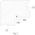
- FIG. 5 is a partial schematic view of the main flexible circuit board in FIG. 4 .
- FIG. 8 is a schematic diagram of the main flexible circuit board in the first state of the display panel according to a fourth embodiment of the present disclosure.
- FIG. 9 is a schematic diagram of the main flexible circuit board in the first state of the display panel according to a fifth embodiment of the present disclosure.
- FIG. 10 is a schematic diagram of the main flexible circuit board and the light-transmissive area in the first state of the display panel in an embodiment of the present disclosure.
- FIG. 11 is a schematic diagram of a chip-on-film flexible circuit board and a flexible touch circuit board of the display panel in an embodiment of the present disclosure.
- Example embodiments will now be described more fully with reference to the accompanying drawings.
- Example embodiments may be embodied in various forms and should not be construed as limited to embodiments set forth herein. Rather, these embodiments are provided so that the present disclosure will be thorough and complete, and will fully convey the concept of example embodiments to those skilled in the art.
- the same reference numerals in the drawings denote the same or similar structures, and thus their detailed descriptions will be omitted.
- the drawings are merely schematic illustrations of the present disclosure and are not necessarily drawn to scale.
- the display panel has a Main Flexible Printed Circuit (MFPC), which is used to transmit the drive signal and the power signal from the main board of the terminal apparatus to the display panel for image display.
- MFPC Main Flexible Printed Circuit
- the display panel needs to be tested by a test device for testing the display panel. For example, when a lighting test is performed by a lighting test device, a test signal may be input to the display panel by the lighting test device to make it present a specific pattern, thereby determining whether the display panel displays normally.
- the test device needs to be connected to the main flexible circuit board of the display panel, in order to input the test signal.
- it is usually necessary to fold the main flexible circuit board so that the connection port thereof extends out of the display panel for connection with the test device.
- it is easy to cause the main flexible circuit board to tear.
- the pressure is too large, the phenomenon of “dead break” that exceeds the elastic limit and cannot be recovered is prone to occur, thus affecting the normal display of the display panel, and even causing the display panel to be scrapped.
- the main flexible circuit board is not folded, it needs to be connected to the test device through an adapter device, which increases the cost, and may still leads to problems such as tearing during connection and detachment of the adapter device.
- Embodiments of the present disclosure provide a display panel.
- the display panel includes a display substrate 1 and a main flexible circuit board 2 .
- the display substrate 1 has a backlight surface 11 .
- the main flexible circuit board 2 includes a connection section 21 , a fixed section 22 , and a test section 23 .
- connection section 21 is disposed on the backlight surface 11 .
- the outer peripheral surface of the connection section 21 includes a first side 211 and a second side 212 that are opposite to each other.
- the fixed section 22 is attached and fixed onto the backlight surface 11 .
- One end of the fixed section 22 is connected to the first side 211 , and the other end of the fixed section 22 extends to an end of the first side 211 away from the second side 212 .
- test section 23 is attached onto the backlight surface 11 , and the connection port 231 is located within an edge of the display substrate 1 .
- the test section 23 may be in the first state when the test is not performed or after the test is completed. At this time, the test section 23 is attached onto the backlight surface, and the connection port 231 is located within the edge of the display substrate 1 , so as to prevent the connection port 231 from protruding out from the edge of the display substrate 1 and interfering with other structures, so that the display panel may be installed normally.
- the depth of the crack relief groove 100 is not greater than 10% of the width of the test section. This helps to prevent the crack relief groove 100 from being too wide and affecting the wiring of the test section 23 . Further, this also helps to avoid that the corner where the test section 23 and the connection section 21 are connected is too narrow, causing the local strength too low.
- the display substrate 1 may have a backlight surface 11 and a light emission surface 12 opposite to each other.
- the light emission surface 12 is configured to emit light for image display.
- the display substrate 1 may be an Organic Light-Emitting Diode (OLED) display substrate, a liquid crystal display substrate, a micro Light-Emitting Diode (micro LED) display substrate, or the like.
- OLED Organic Light-Emitting Diode
- the display substrate 1 includes a drive backplane 101 and a light-emitting device layer 102 disposed on one side of the drive backplane 101 .
- the light-emitting device layer 102 may include a plurality of light-emitting units.
- the drive backplane 101 may drive each light-emitting unit to emit light independently for image display.
- the specific display principle will not be described in detail here.
- the backlight surface 11 may be a surface of the drive backplane 101 facing away from the light-emitting device layer 102 .
- the light emission surface 12 may be a surface of the light-emitting device layer 102 facing away from the drive backplane 101 .
- the outer peripheral surface of the connection section 21 may include a first side 211 and a second side 212 opposite to each other.
- the first side 211 may extend in a direction parallel to one side of the display substrate 1 .
- the orthographic projection of the connection section 21 on the backlight surface 11 is a rectangle.
- the first side 211 and the second side 212 may be sides corresponding to two opposite sides of the rectangle.
- the distance between the first side 211 and the second side 212 is not particularly limited here.
- the distance between the first side 211 and the second side 212 may be from 8 mm to 12 mm, such as 10.7 mm.
- connection port 231 The specific structure of the connection port 231 depends on the test device 001 to be connected, which is not specified here, as long as it can be connected to the test device 001 in a pluggable way and can transmit test signals.
- the test section 23 is a flexible structure, and the test section 23 may also be a flexible structure.
- the test section 23 may include a flexible substrate made of polyimide or other flexible materials, and further include a circuit formed on the flexible substrate.
- the orthographic projection of the crack relief groove 100 on the backlight surface 11 is arc-shaped, such as in a circular arc or an elliptical arc shape.
- the first side 211 and the side of the test section 23 close to the fixed section 22 are planes perpendicular to each other.
- the orthographic projection of the crack relief groove 100 on the backlight surface 11 is U-shaped.
- the crack relief groove 100 has two opposite side walls. One side wall of the crack relief groove 100 is coplanar with the side of the test section 23 close to the fixed section 22 , and the other side wall of the crack relief groove 100 intersects with the first side 211 , where the intersection may be a perpendicular intersection.
- the number of crack relief grooves 100 is two, and the orthographic projections of the two crack relief grooves 100 on the backlight surface 11 are both U-shaped.
- the U-shaped openings are oriented perpendicular to each other.
- the crack relief groove 100 has two opposite side walls, and the distance between the two side walls gradually decreases toward the second side 212 .
- the orthographic projection of the crack relief groove 100 on the backlight surface 11 is in a V shape, and the two side walls are two intersecting planes with an included angle less than 90°.
- the orthographic projection of the connection section 21 on the backlight surface 11 is a rectangle
- the first side 211 corresponds to a long side of the rectangle
- the extension direction of the orthographic projection of the first side 211 on the backlight surface 11 is the longitudinal direction of the rectangle.
- the width of the test section 23 in the longitudinal direction is 10.4 mm
- the orthographic projection of the crack relief groove 100 on the backlight surface 11 and the orthographic projection of the transition surface 200 on the backlight surface 11 are arcs with a radius of 0.5 mm. That is, the depth of the crack relief groove 100 in the longitudinal direction is 1 mm.
- the display panel in an embodiment of the present disclosure may also have an under-screen fingerprint recognition function.
- the display substrate 1 may have a light-transmissive area 300 .
- the light-transmissive area 300 may be an open structure, a transparent solid structure.
- the display panel may further include a fingerprint sense unit 3 .
- the fingerprint sense unit 3 may be arranged on the backlight surface 11 .
- the light-transmissive area 300 is located within the projection of the fingerprint sense unit 3 on the backlight surface 11 .
- the fingerprint sense unit 3 may include a photoelectric sensor, used to sense the light reflected by the valley ridges of the fingers, for generating a signal reflecting the fingerprint information.
- the side of the fixed section 22 close to the test section 23 may be provided with an avoidance hole 221 .
- the avoidance hole 221 penetrates through the fixed section 22 in a direction perpendicular to the backlight surface 11 .
- a partial outline of the light-transmissive area 300 is located in the avoidance hole 221 and matches the avoidance hole 221 in shape.
- the display panel in an embodiment of the present disclosure may further include a chip-on-film (COF) flexible circuit board 6 .
- the chip-on-film flexible circuit board 6 is connected to the display substrate 1 , folded to the backlight surface 11 , and connected with the fixed section 22 .
Landscapes
- Engineering & Computer Science (AREA)
- Microelectronics & Electronic Packaging (AREA)
- Physics & Mathematics (AREA)
- Computer Hardware Design (AREA)
- General Physics & Mathematics (AREA)
- Theoretical Computer Science (AREA)
- Devices For Indicating Variable Information By Combining Individual Elements (AREA)
Abstract
Description
Claims (19)
Applications Claiming Priority (3)
| Application Number | Priority Date | Filing Date | Title |
|---|---|---|---|
| CN202010568363.0 | 2020-06-19 | ||
| CN202010568363.0A CN113825297B (en) | 2020-06-19 | 2020-06-19 | Display panel, display device and terminal equipment |
| PCT/CN2021/094718 WO2021254081A1 (en) | 2020-06-19 | 2021-05-19 | Display panel, display device and terminal apparatus |
Publications (2)
| Publication Number | Publication Date |
|---|---|
| US20220330416A1 US20220330416A1 (en) | 2022-10-13 |
| US12035463B2 true US12035463B2 (en) | 2024-07-09 |
Family
ID=78924804
Family Applications (1)
| Application Number | Title | Priority Date | Filing Date |
|---|---|---|---|
| US17/761,662 Active 2042-04-13 US12035463B2 (en) | 2020-06-19 | 2021-05-19 | Display panel, display device and terminal apparatus |
Country Status (3)
| Country | Link |
|---|---|
| US (1) | US12035463B2 (en) |
| CN (1) | CN113825297B (en) |
| WO (1) | WO2021254081A1 (en) |
Families Citing this family (1)
| Publication number | Priority date | Publication date | Assignee | Title |
|---|---|---|---|---|
| TWI863762B (en) * | 2023-12-19 | 2024-11-21 | 頎邦科技股份有限公司 | Flexible circuit board |
Citations (10)
| Publication number | Priority date | Publication date | Assignee | Title |
|---|---|---|---|---|
| US20080074853A1 (en) * | 2006-09-22 | 2008-03-27 | Jang Jin-Seok | Flexible printed circuit board |
| US20110037717A1 (en) | 2009-08-11 | 2011-02-17 | Au Optronics Corporation | Backlight Module with Low Electromagnetic Interference and Display Device Using the Same |
| CN204069479U (en) | 2014-07-14 | 2014-12-31 | 联想(北京)有限公司 | Flexible circuit board FPC and electronic equipment |
| US20150036300A1 (en) * | 2013-07-30 | 2015-02-05 | Lg Display Co., Ltd. | Display device and method of manufacturing the same |
| CN104703388A (en) | 2015-02-24 | 2015-06-10 | 友达光电股份有限公司 | Flexible circuit board and curved display device using same |
| CN204578894U (en) | 2015-04-23 | 2015-08-19 | 南昌欧菲显示科技有限公司 | Be applied to pad structure and the LCM backlight display module of the backlight FPC of LCM |
| CN207283905U (en) | 2017-09-11 | 2018-04-27 | 深圳市汇晨电子股份有限公司 | A kind of flexible PCB for avoiding tearing after bending |
| CN110049616A (en) | 2019-04-10 | 2019-07-23 | 上海摩软通讯技术有限公司 | A kind of flexible circuit board |
| CN209930344U (en) | 2019-08-22 | 2020-01-10 | 南京视倍安智能科技有限公司 | Detection device is lighted automatically after reverse book of cell-phone display screen FPC |
| CN212086585U (en) | 2020-06-19 | 2020-12-04 | 京东方科技集团股份有限公司 | Display panel, display device and terminal equipment |
Family Cites Families (5)
| Publication number | Priority date | Publication date | Assignee | Title |
|---|---|---|---|---|
| JP4884746B2 (en) * | 2005-10-20 | 2012-02-29 | 株式会社 日立ディスプレイズ | Liquid crystal display |
| JP2007127742A (en) * | 2005-11-02 | 2007-05-24 | Funai Electric Co Ltd | Liquid crystal display device |
| CN204836778U (en) * | 2015-07-02 | 2015-12-02 | 上达电子(深圳)有限公司 | Flexible circuit board |
| KR102633441B1 (en) * | 2018-12-03 | 2024-02-06 | 삼성디스플레이 주식회사 | Display unit, electronic apparatus including the same, and method of manufacturing the electronic apparatus |
| CN110850634A (en) * | 2019-11-05 | 2020-02-28 | 武汉华星光电技术有限公司 | Backlight module and liquid crystal display panel |
-
2020
- 2020-06-19 CN CN202010568363.0A patent/CN113825297B/en active Active
-
2021
- 2021-05-19 WO PCT/CN2021/094718 patent/WO2021254081A1/en not_active Ceased
- 2021-05-19 US US17/761,662 patent/US12035463B2/en active Active
Patent Citations (12)
| Publication number | Priority date | Publication date | Assignee | Title |
|---|---|---|---|---|
| US20080074853A1 (en) * | 2006-09-22 | 2008-03-27 | Jang Jin-Seok | Flexible printed circuit board |
| US20110037717A1 (en) | 2009-08-11 | 2011-02-17 | Au Optronics Corporation | Backlight Module with Low Electromagnetic Interference and Display Device Using the Same |
| US9256338B2 (en) | 2009-08-11 | 2016-02-09 | Au Optronics Corporation | Backlight module with low electromagnetic interference and display device using the same |
| US20160109989A1 (en) | 2009-08-11 | 2016-04-21 | Au Optronics Corporation | Backlight Module with Low Electromagnetic Interference and Display Device Using the Same |
| US20150036300A1 (en) * | 2013-07-30 | 2015-02-05 | Lg Display Co., Ltd. | Display device and method of manufacturing the same |
| CN204069479U (en) | 2014-07-14 | 2014-12-31 | 联想(北京)有限公司 | Flexible circuit board FPC and electronic equipment |
| CN104703388A (en) | 2015-02-24 | 2015-06-10 | 友达光电股份有限公司 | Flexible circuit board and curved display device using same |
| CN204578894U (en) | 2015-04-23 | 2015-08-19 | 南昌欧菲显示科技有限公司 | Be applied to pad structure and the LCM backlight display module of the backlight FPC of LCM |
| CN207283905U (en) | 2017-09-11 | 2018-04-27 | 深圳市汇晨电子股份有限公司 | A kind of flexible PCB for avoiding tearing after bending |
| CN110049616A (en) | 2019-04-10 | 2019-07-23 | 上海摩软通讯技术有限公司 | A kind of flexible circuit board |
| CN209930344U (en) | 2019-08-22 | 2020-01-10 | 南京视倍安智能科技有限公司 | Detection device is lighted automatically after reverse book of cell-phone display screen FPC |
| CN212086585U (en) | 2020-06-19 | 2020-12-04 | 京东方科技集团股份有限公司 | Display panel, display device and terminal equipment |
Non-Patent Citations (1)
| Title |
|---|
| International Search Report and Written Opinion for International Application No. PCT/CN2021/094718 mailed Jul. 27, 2021. |
Also Published As
| Publication number | Publication date |
|---|---|
| CN113825297A (en) | 2021-12-21 |
| CN113825297B (en) | 2025-10-31 |
| WO2021254081A1 (en) | 2021-12-23 |
| US20220330416A1 (en) | 2022-10-13 |
Similar Documents
| Publication | Publication Date | Title |
|---|---|---|
| US11221645B2 (en) | Display device and method of manufacturing the same | |
| US6411353B1 (en) | Liquid crystal display device with its upper and lower cases clamped by crimping portions thereof | |
| JP2010085923A (en) | Display device | |
| KR20160085388A (en) | Display device | |
| JP2015005288A (en) | Touch display panel, and touch display device | |
| KR102600528B1 (en) | Display device | |
| JP2013025783A (en) | Touch panel | |
| US20220130912A1 (en) | Display device and method for manufacturing the same | |
| US12035463B2 (en) | Display panel, display device and terminal apparatus | |
| CN108493212A (en) | Flexible Displays structure and electronic equipment | |
| CN212086585U (en) | Display panel, display device and terminal equipment | |
| JP5086662B2 (en) | Display device | |
| US8681091B2 (en) | Bistable display device | |
| US20220132667A1 (en) | Electronic device | |
| KR20100055989A (en) | Liquid crystal display device | |
| KR20110012212A (en) | Touch screen with a structure where the upper and lower panels of the touch panel are bonded without bending by separating the upper and lower terminals of the double-sided FPC and the manufacturing method thereof | |
| CN109496067B (en) | Flexible circuit board, display panel and display device | |
| US20240074043A1 (en) | Flexible circuit board and display device | |
| CN205196083U (en) | Flexible circuit board | |
| US10925156B2 (en) | Circuit board structure and display panel | |
| US20190354219A1 (en) | Display device | |
| JP2006235252A (en) | Display device | |
| KR20230010128A (en) | Display device | |
| JP2007292838A (en) | Display device | |
| US12124646B2 (en) | Display panel |
Legal Events
| Date | Code | Title | Description |
|---|---|---|---|
| FEPP | Fee payment procedure |
Free format text: ENTITY STATUS SET TO UNDISCOUNTED (ORIGINAL EVENT CODE: BIG.); ENTITY STATUS OF PATENT OWNER: LARGE ENTITY |
|
| AS | Assignment |
Owner name: BOE TECHNOLOGY GROUP CO., LTD., CHINA Free format text: ASSIGNMENT OF ASSIGNORS INTEREST;ASSIGNORS:ZHANG, SHUANG;HUANG, XIAOXIA;JI, BING;REEL/FRAME:060406/0556 Effective date: 20220308 Owner name: CHENGDU BOE OPTOELECTRONICS TECHNOLOGY CO., LTD., CHINA Free format text: ASSIGNMENT OF ASSIGNORS INTEREST;ASSIGNORS:ZHANG, SHUANG;HUANG, XIAOXIA;JI, BING;REEL/FRAME:060406/0556 Effective date: 20220308 |
|
| STPP | Information on status: patent application and granting procedure in general |
Free format text: DOCKETED NEW CASE - READY FOR EXAMINATION |
|
| STPP | Information on status: patent application and granting procedure in general |
Free format text: NOTICE OF ALLOWANCE MAILED -- APPLICATION RECEIVED IN OFFICE OF PUBLICATIONS |
|
| STPP | Information on status: patent application and granting procedure in general |
Free format text: PUBLICATIONS -- ISSUE FEE PAYMENT RECEIVED |
|
| STPP | Information on status: patent application and granting procedure in general |
Free format text: PUBLICATIONS -- ISSUE FEE PAYMENT VERIFIED |
|
| STCF | Information on status: patent grant |
Free format text: PATENTED CASE |