US12004345B2 - Semiconductor with extended life time flash memory and fabrication method thereof - Google Patents
Semiconductor with extended life time flash memory and fabrication method thereof Download PDFInfo
- Publication number
- US12004345B2 US12004345B2 US17/538,000 US202117538000A US12004345B2 US 12004345 B2 US12004345 B2 US 12004345B2 US 202117538000 A US202117538000 A US 202117538000A US 12004345 B2 US12004345 B2 US 12004345B2
- Authority
- US
- United States
- Prior art keywords
- layer
- erasing
- floating gate
- sacrificial
- receiving portion
- Prior art date
- Legal status (The legal status is an assumption and is not a legal conclusion. Google has not performed a legal analysis and makes no representation as to the accuracy of the status listed.)
- Active, expires
Links
Images


Classifications
-
- H—ELECTRICITY
- H10—SEMICONDUCTOR DEVICES; ELECTRIC SOLID-STATE DEVICES NOT OTHERWISE PROVIDED FOR
- H10B—ELECTRONIC MEMORY DEVICES
- H10B41/00—Electrically erasable-and-programmable ROM [EEPROM] devices comprising floating gates
- H10B41/20—Electrically erasable-and-programmable ROM [EEPROM] devices comprising floating gates characterised by three-dimensional arrangements, e.g. with cells on different height levels
- H10B41/23—Electrically erasable-and-programmable ROM [EEPROM] devices comprising floating gates characterised by three-dimensional arrangements, e.g. with cells on different height levels with source and drain on different levels, e.g. with sloping channels
- H10B41/27—Electrically erasable-and-programmable ROM [EEPROM] devices comprising floating gates characterised by three-dimensional arrangements, e.g. with cells on different height levels with source and drain on different levels, e.g. with sloping channels the channels comprising vertical portions, e.g. U-shaped channels
-
- H—ELECTRICITY
- H10—SEMICONDUCTOR DEVICES; ELECTRIC SOLID-STATE DEVICES NOT OTHERWISE PROVIDED FOR
- H10B—ELECTRONIC MEMORY DEVICES
- H10B41/00—Electrically erasable-and-programmable ROM [EEPROM] devices comprising floating gates
-
- H—ELECTRICITY
- H10—SEMICONDUCTOR DEVICES; ELECTRIC SOLID-STATE DEVICES NOT OTHERWISE PROVIDED FOR
- H10D—INORGANIC ELECTRIC SEMICONDUCTOR DEVICES
- H10D64/00—Electrodes of devices having potential barriers
- H10D64/01—Manufacture or treatment
- H10D64/031—Manufacture or treatment of data-storage electrodes
- H10D64/035—Manufacture or treatment of data-storage electrodes comprising conductor-insulator-conductor-insulator-semiconductor structures
-
- H—ELECTRICITY
- H01—ELECTRIC ELEMENTS
- H01L—SEMICONDUCTOR DEVICES NOT COVERED BY CLASS H10
- H01L25/00—Assemblies consisting of a plurality of semiconductor or other solid state devices
- H01L25/03—Assemblies consisting of a plurality of semiconductor or other solid state devices all the devices being of a type provided for in a single subclass of subclasses H10B, H10D, H10F, H10H, H10K or H10N, e.g. assemblies of rectifier diodes
- H01L25/04—Assemblies consisting of a plurality of semiconductor or other solid state devices all the devices being of a type provided for in a single subclass of subclasses H10B, H10D, H10F, H10H, H10K or H10N, e.g. assemblies of rectifier diodes the devices not having separate containers
- H01L25/07—Assemblies consisting of a plurality of semiconductor or other solid state devices all the devices being of a type provided for in a single subclass of subclasses H10B, H10D, H10F, H10H, H10K or H10N, e.g. assemblies of rectifier diodes the devices not having separate containers the devices being of a type provided for in group subclass H10D
- H01L25/074—Stacked arrangements of non-apertured devices
-
- H01L29/42324—
-
- H01L29/66825—
-
- H01L29/788—
-
- H—ELECTRICITY
- H10—SEMICONDUCTOR DEVICES; ELECTRIC SOLID-STATE DEVICES NOT OTHERWISE PROVIDED FOR
- H10B—ELECTRONIC MEMORY DEVICES
- H10B41/00—Electrically erasable-and-programmable ROM [EEPROM] devices comprising floating gates
- H10B41/10—Electrically erasable-and-programmable ROM [EEPROM] devices comprising floating gates characterised by the top-view layout
-
- H—ELECTRICITY
- H10—SEMICONDUCTOR DEVICES; ELECTRIC SOLID-STATE DEVICES NOT OTHERWISE PROVIDED FOR
- H10B—ELECTRONIC MEMORY DEVICES
- H10B41/00—Electrically erasable-and-programmable ROM [EEPROM] devices comprising floating gates
- H10B41/20—Electrically erasable-and-programmable ROM [EEPROM] devices comprising floating gates characterised by three-dimensional arrangements, e.g. with cells on different height levels
-
- H—ELECTRICITY
- H10—SEMICONDUCTOR DEVICES; ELECTRIC SOLID-STATE DEVICES NOT OTHERWISE PROVIDED FOR
- H10B—ELECTRONIC MEMORY DEVICES
- H10B41/00—Electrically erasable-and-programmable ROM [EEPROM] devices comprising floating gates
- H10B41/30—Electrically erasable-and-programmable ROM [EEPROM] devices comprising floating gates characterised by the memory core region
-
- H—ELECTRICITY
- H10—SEMICONDUCTOR DEVICES; ELECTRIC SOLID-STATE DEVICES NOT OTHERWISE PROVIDED FOR
- H10D—INORGANIC ELECTRIC SEMICONDUCTOR DEVICES
- H10D30/00—Field-effect transistors [FET]
- H10D30/01—Manufacture or treatment
- H10D30/021—Manufacture or treatment of FETs having insulated gates [IGFET]
- H10D30/0411—Manufacture or treatment of FETs having insulated gates [IGFET] of FETs having floating gates
-
- H—ELECTRICITY
- H10—SEMICONDUCTOR DEVICES; ELECTRIC SOLID-STATE DEVICES NOT OTHERWISE PROVIDED FOR
- H10D—INORGANIC ELECTRIC SEMICONDUCTOR DEVICES
- H10D30/00—Field-effect transistors [FET]
- H10D30/60—Insulated-gate field-effect transistors [IGFET]
- H10D30/68—Floating-gate IGFETs
-
- H—ELECTRICITY
- H10—SEMICONDUCTOR DEVICES; ELECTRIC SOLID-STATE DEVICES NOT OTHERWISE PROVIDED FOR
- H10D—INORGANIC ELECTRIC SEMICONDUCTOR DEVICES
- H10D30/00—Field-effect transistors [FET]
- H10D30/60—Insulated-gate field-effect transistors [IGFET]
- H10D30/68—Floating-gate IGFETs
- H10D30/689—Vertical floating-gate IGFETs
-
- H—ELECTRICITY
- H10—SEMICONDUCTOR DEVICES; ELECTRIC SOLID-STATE DEVICES NOT OTHERWISE PROVIDED FOR
- H10D—INORGANIC ELECTRIC SEMICONDUCTOR DEVICES
- H10D30/00—Field-effect transistors [FET]
- H10D30/60—Insulated-gate field-effect transistors [IGFET]
- H10D30/68—Floating-gate IGFETs
- H10D30/6891—Floating-gate IGFETs characterised by the shapes, relative sizes or dispositions of the floating gate electrode
-
- H10W90/00—
Definitions
- the subject matter herein generally relates to semiconductor memory.
- three-dimensional (3D) flash can store data for a long period without being powered, and has advantages of high-density, fast storing speed, and ease of erasing and rewriting. While storing or erasing data in the 3D flash, based on the voltage between a floating gate and a control gate, electrons move between the floating gate and a channel layer by passing through a tunnel dielectric layer. During repeated storing and erasing data in the 3D flash, the performance of the tunnel dielectric layer is reduced, reducing the effective function of the 3D flash.
- FIG. 1 is a diagram illustrating an embodiment of a semiconductor along a horizontal direction.
- FIG. 2 is a diagram illustrating an embodiment of the semiconductor along a vertical direction.
- FIG. 3 is a diagram illustrating an embodiment of the erasing layer along the horizontal direction.
- FIG. 4 is a flowchart illustrating an embodiment of a method for fabricating the semiconductor.
- FIG. 5 is a diagram illustrating an embodiment of the vertical structures in block S 10 of FIG. 4 .
- FIG. 6 is a diagram illustrating an embodiment of the vertical structures in block S 11 of FIG. 4 .
- FIG. 7 is a diagram illustrating an embodiment of the vertical structures in block S 12 of FIG. 4 .
- FIG. 8 is a diagram illustrating an embodiment of the vertical structures in block S 13 of FIG. 4 .
- FIG. 9 is a diagram illustrating an embodiment of the vertical structures in block S 14 of FIG. 4 .
- FIG. 10 is a diagram illustrating an embodiment of the vertical structures in block S 15 of FIG. 4 .
- module refers to logic embodied in hardware or firmware, or to a collection of software instructions, written in a programming language, for example, Java, C, or assembly.
- One or more software instructions in the modules may be embedded in firmware, such as an EPROM, magnetic, or optical drives.
- modules may comprise connected logic units, such as gates and flip-flops, and may comprise programmable units, such as programmable gate arrays or processors, such as a CPU.
- the modules described herein may be implemented as either software and/or hardware modules and may be stored in any type of computer-readable medium or other computer storage systems.
- the present disclosure provides a semiconductor and a method for fabricating the semiconductor for reducing a dissipation of the tunnel dielectric layer while storing or erasing data.
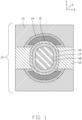
- FIG. 1 shows a semiconductor 1 taken along a horizontal direction.
- FIG. 2 shows the semiconductor 1 taken along a vertical direction.
- the semiconductor 1 in a stack structure includes a plurality of storing cells 10 .
- FIG. 1 only shows one storing cell 10
- FIG. 2 show two adjacent storing cells 10 .
- the semiconductor 1 can be a three-dimensional (3D) flash.
- Each storing cell 10 can be implemented to store data or allow erasure of data.
- Each storing cell 10 includes a stack structure ST, a receiving space OP (as shown in FIG. 6 ), an insulating layer 12 , a floating gate layer 15 , a blocking layer 14 , a tunnel dielectric layer 16 , a channel layer 17 , and a filling layer 18 .
- the stack structure ST includes several control gate layers 13 , several dielectric layers 11 , and several erasing layers 112 .
- the stack structure ST includes two control gate layers 13 , three dielectric layers 11 , and three erasing layers 112 .
- the topmost and bottommost dielectric layers 11 are respectively the top layer and the bottom layer.
- the reset dielectric layer 11 is the middle layer.
- Each control gate layer 13 is sandwiched between two adjacent dielectric layers 11 .
- Each erasing layer 112 is separated from the control gate layer 13 by the dielectric layer 11 .
- the erasing layer 112 is separated from the floating gate layer 15 by the dielectric layer 11 and the blocking layer 14 .
- the blocking layer 14 , the tunnel dielectric layer 16 , the channel layer 17 , and the filling layer 18 inside the control gate layer 13 are substantially annular in shape (as shown in FIG. 1 ).
- the control gate layer 13 is made of conductive material.
- the erasing layer 112 is insulated from the corresponding control gate layer 13 by the dielectric layer 11 .
- the erasing layer 112 is insulated from the floating gate layer 15 by the dielectric layer 11 and the blocking layer 14 .
- the erasing layer 112 is insulated from the channel layer 17 in the receiving space OP by the dielectric layer 11 and the blocking layer 14 .
- the filling layer 18 can be made of dielectric material, and is insulated from the adjacent channel layer 17 .
- FIG. 3 shows the erasing layer 112 of the storing cells 10 in a 2*2 matrix.
- the erasing layer 112 is coplanar with and in contact with the erasing layer 112 in another adjacent storing cell 10 in a whole shape technology.
- the second horizontal direction Y is perpendicular to the first vertical direction X.
- the erasing layers 112 in different storing cells 10 are in contact with each other to form a specified pattern P.
- the specified pattern P include two first portions P 1 parallel with each other along the second horizontal direction Y, and at least two second portions P 2 parallel with each along a third direction Z.
- the first vertical direction X, the second horizontal direction Y, and the third direction Z are all perpendicular to each other to form a three-dimensional coordinate system. At least one end of the second portion P 2 is in contact with the first portion P 1 . In one embodiment, both ends of the second portion P 2 are in contact with the first portion P 1 .
- the first portion P 1 establishes an electrical connection between the erasing layer 112 and an external circuit.
- the erasing layer 112 is made of conductive material with low resistance, such as metal, silicide, the dielectric layer 11 is made of insulating material.
- the receiving space OP crosses the middle portion of the stack structure ST.
- the receiving space OP includes a first receiving portion OP 1 and several second receiving portions OP 2 .
- the first receiving portion OP 1 crosses through the stack structure ST along the first vertical direction X.
- the second receiving portion OP 2 communicates with the first receiving portion OP 1 .
- the second receiving portions OP 2 extend from the first receiving portion OP 1 to the control gate layer 13 along the second horizontal direction Y.
- the second receiving portions OP 2 are symmetrically disposed on opposite sides of the first receiving portion OP 1 .
- a part of the blocking layer 14 is received in the second receiving portion OP 2 , and the rest of the blocking layer 14 is receiving in the first receiving OP 1 .
- the blocking layer 14 is coplanar with the control gate layer 13 .
- a double thickness of the blocking layer 14 is less than a thickness of the control gate layer 13 , the blocking layer 14 is completely received in the second receiving portion OP 2 , and a space (not labeled) for receiving the floating gate layer 15 .
- the blocking layer 14 in the first receiving portion OP 1 is parallel with the first vertical direction X.
- the floating gate layer 15 is received in the space of the blocking layer 14 , and in the second receiving portion OP 2 .
- the floating gate layer 15 is coplanar with the control gate layer 13 .
- the floating gate layer 15 is substantially in the shape of half a circle (or half of an oval, as shown in FIG. 1 ).
- the floating gate layer 15 is partly overlapped with the erasing layer 112 .
- the floating gate layer 15 is made of conductive material such as silicide.
- the floating gate layer 15 is used for storing data.
- the tunnel dielectric layer 16 is received in the first receiving portion OP 1 , and sidewall of the tunnel dielectric layer 16 is covered by the blocking layer 14 and the floating gate layer 15 along the first vertical direction X.
- the tunnel dielectric layer 16 is substantially in an annular shape (as shown in FIG. 1 ).
- the channel layer 17 is disposed in the first receiving portion OP 1 , and is sandwiched between the tunnel dielectric layer 16 and the filling layer 18 .
- the channel layer 17 is substantially in an annular shape (as shown in FIG. 1 ).
- the channel layer 17 is made of silicon or other semiconductor material.
- the filling layer 18 fills the empty part of the first receiving portion OP 1 .
- the filling layer 18 is made of insulation material.
- the storing cell 10 further includes the insulating layer 12 .
- the insulating layer 12 insulates the blocking layer 14 disposed on opposite side of the receiving space OP along the second horizontal direction Y, and insulates the tunnel dielectric layers in adjacent storing cells 10 along the third direction Z.
- the insulating layer 12 is made of silicon oxide material.
- a storing operation of the storing cell 10 is the same as in a normal semiconductor device. For example, when the voltage is applied on the control gate layer 13 , electrons moves along a data writing path (path-A) from the channel layer 17 into the floating gate layer 15 through the tunnel dielectric layer 16 , thus data is received in the storing cell 10 .
- path-A data writing path
- a positive voltage is applied on the erasing layer 112 , the floating gate layer 15 floats, a voltage less than the positive voltage is applied on the control gate layer 13 , thus a punch-through between the erasing layer 112 and the control gate layer 13 is avoided.
- a ground voltage or negative voltage
- the electrons move along a data erasing path (path-B) from the floating gate layer 15 to the erasing layer 112 through the portion of the dielectric layer 11 , which is overlapped with the erasing layer 112 and the floating gate layer 15 , and the sidewall of the blocking layer 14 .
- Such electrons do not pass through the tunnel dielectric layer 16 .
- the positive voltage is in a range from 10-15 volts (V).
- the erasing layer 112 being overlapped with the floating gate layer 15 along the first vertical direction X in the structure of the semiconductor causes the electrons to move along the path-B, a path different from the data writing path path-A.
- Even repeated data writing and data erasing processes cause less dissipation of the tunnel dielectric layer 16 in the storing cell 10 , and a life time of the semiconductor 1 is extended.
- FIG. 4 shows a flowchart of a method for manufacturing the above semiconductor.
- a method for fabricating the semiconductor 1 may comprise at least the following steps, which may be followed in a different order:
- a stack structure ST with at least one first sacrificial layer 19 a , at least one dielectric layer 11 , and at least one second sacrificial layer 19 b is provided.
- the stack structure ST includes two first sacrificial layers 19 a , three dielectric layers 11 , and three second sacrificial layers 19 b .
- the two first sacrificial layers 19 a are separated from each other by the dielectric layer 11 .
- the dielectric layer 11 is formed in depositing and flattening manner.
- the dielectric layer 11 is etched and patterned to form the second sacrificial layers 19 b in a first material, and after the second sacrificial layers 19 b are formed, the depositing process is continued to form the dielectric layer 11 for separating the first sacrificial layer 19 a and the second sacrificial layer 19 b , and then the first sacrificial layer 19 a is formed on the deposited dielectric layer 11 .
- the above processes are repeatedly to form the stack structure ST.
- the topmost and bottommost dielectric layers 11 are the top layer and the bottom layer, and the rest of the dielectric layers 11 is the middle layer.
- the control gate layer 13 is sandwiched between two adjacent dielectric layer 11 .
- the second sacrificial layer 19 b is insulated from the first sacrificial layer 19 a by the dielectric layer 11 .
- Each second sacrificial layer 19 b is in a specified pattern P.
- the second sacrificial layers 19 b are arranged in a 2*2 matrix.
- the specified pattern P include two parallel first portions P 1 along second horizontal direction Y and at least two parallel second portions P 2 along a third direction Z.
- the first portion P 1 can be divided into more second sacrificial layers 19 b in the storing cells 10 .
- At least one end of the second portion P 2 is in contact with the first portion P 1 .
- both ends of the second portion P 2 is in contact with the first portion P 1 .
- the first material can be silicon nitride
- the dielectric layer 11 is made of insulation material.
- the stack structure ST is etched to form a receiving space (op).
- the stack structure ST is divided into several storing regions 101 in a same size. Each storing region 101 correspond to a storing cell 10 .
- the receiving space OP crosses the middle portion of the stack structure ST in one storing region 101 .
- the receiving space OP includes a first receiving portion OP 1 and several receiving portions OP 2 .
- the first receiving portion OP 1 crosses through the stack structure ST along the first vertical direction X.
- the second receiving portion OP 2 communicates with the first receiving portion OP 1 .
- the second receiving portions OP 2 are extended from the first receiving portion OP 1 to the control gate layer 13 along the second horizontal direction Y. In one embodiment, there are four second receiving portions OP 2 .
- the second receiving portions OP 2 are symmetrically disposed on opposite sides of the first receiving portion OP 1 .
- the second receiving portion OP 2 is overlapped with the second sacrificial layer 19 b
- the first sacrificial layer 19 a is overlapped with the second sacrificial layer 19 b.
- a blocking layer 14 and a floating gate layer 15 is formed in the receiving space 15 .
- a partial of the blocking layer 14 is received in the second receiving portion OP 2 , and is coplanar with the first sacrificial layer 19 a for covering a sidewall of the first sacrificial layer 19 a .
- a partial of the blocking layer 14 is parallel with the first vertical direction X.
- the blocking layer 14 is overlapped with the second sacrificial layer 19 b .
- the floating gate layer 15 is received in the inside of the blocking layer 14 being received in the second receiving portion 19 b .
- the floating gate layer 15 is coplanar with the control gate layer 13 .
- a partial of the floating gate layer 15 is parallel with the first vertical direction X.
- the floating gate 15 is made of conductivity material, such as silicide.
- a partial of the floating gate layer 15 received in the first receiving portion OP 1 is removed, for ensuring the rest of the floating gate layer 15 being completely received in the second receiving portion OP 2 as shown in FIG. 8 .
- a tunnel dielectric layer 16 , a channel layer 17 , and a filling layer 18 are formed in that order in the first receiving portion OP 1 .
- the tunnel dielectric layer 16 is received in the first receiving portion OP 1 , and covers sidewalls of the blocking layer 14 and the floating gate layer 15 along the first vertical direction X.
- the channel layer 17 is received in the first receiving portion OP 1 .
- the channel layer 17 is disposed on an inner side of the tunnel dielectric layer 16 .
- the channel layer 17 is made of semiconductor material, such as SI.
- the filling layer 18 fills the rest space of the receiving portion OP 1 .
- the filling layer 18 is made of insulation material.
- control gate layers 13 are formed at the positions of the removed first sacrificial layer 19 a
- the erasing layers 112 are formed at the positions of the removed second sacrificial layers 19 b , to form the semiconductor 1 .
- control gate layer 13 and the erasing layer 112 are formed by filling the positions of the removed made of a second material.
- the second material is made of conductive material with low resistance, such as metal or silicide.
- control gate layer 13 While executing a data writing process, the control gate layer 13 is being applied with a voltage, and electron moves from the channel layer 17 into the floating gate layer 15 by passing through the tunnel dielectric layer 16 , for storing data.
- a positive voltage is applied on the erasing layer 112 , the floating gate layer 15 floats, a voltage less than the positive voltage is applied on the control gate layer 13 , thus a punch-through between the erasing layer 112 and the control gate layer 13 is avoided.
- a ground voltage or a negative voltage is applied on the channel layer 17 , and the electron moves along a data erasing path path-B from the floating gate layer 15 to the erasing layer 112 through the portion of the dielectric layer 11 , which is overlapped with the erasing layer 112 and the floating gate layer 15 , and the sidewall of the blocking layer 14 , Such electrons do not pass through the tunnel dielectric layer 16 .
- the positive voltage is in a range from 10-15 volts (V).
- the erasing layer 112 being overlapped with the floating gate layer 15 along the first vertical direction X causes the electrons to move along the path-B, a path different from the data writing path path-A.
- Even repeated data writing and data erasing processes cause less dissipation of the tunnel dielectric layer 16 in the storing cell 10 , and a life time of the semiconductor 1 is extended.
Landscapes
- Engineering & Computer Science (AREA)
- Power Engineering (AREA)
- Microelectronics & Electronic Packaging (AREA)
- Non-Volatile Memory (AREA)
- Physics & Mathematics (AREA)
- Condensed Matter Physics & Semiconductors (AREA)
- General Physics & Mathematics (AREA)
- Computer Hardware Design (AREA)
Abstract
Description
Claims (5)
Priority Applications (1)
| Application Number | Priority Date | Filing Date | Title |
|---|---|---|---|
| US18/649,949 US20240284667A1 (en) | 2021-02-01 | 2024-04-29 | Semiconductor with extended life time flash memory |
Applications Claiming Priority (2)
| Application Number | Priority Date | Filing Date | Title |
|---|---|---|---|
| CN202110139342.1A CN114843275B (en) | 2021-02-01 | 2021-02-01 | Semiconductor device and method for manufacturing semiconductor device |
| CN202110139342.1 | 2021-02-01 |
Related Child Applications (1)
| Application Number | Title | Priority Date | Filing Date |
|---|---|---|---|
| US18/649,949 Division US20240284667A1 (en) | 2021-02-01 | 2024-04-29 | Semiconductor with extended life time flash memory |
Publications (2)
| Publication Number | Publication Date |
|---|---|
| US20220246629A1 US20220246629A1 (en) | 2022-08-04 |
| US12004345B2 true US12004345B2 (en) | 2024-06-04 |
Family
ID=82560870
Family Applications (2)
| Application Number | Title | Priority Date | Filing Date |
|---|---|---|---|
| US17/538,000 Active 2042-04-29 US12004345B2 (en) | 2021-02-01 | 2021-11-30 | Semiconductor with extended life time flash memory and fabrication method thereof |
| US18/649,949 Pending US20240284667A1 (en) | 2021-02-01 | 2024-04-29 | Semiconductor with extended life time flash memory |
Family Applications After (1)
| Application Number | Title | Priority Date | Filing Date |
|---|---|---|---|
| US18/649,949 Pending US20240284667A1 (en) | 2021-02-01 | 2024-04-29 | Semiconductor with extended life time flash memory |
Country Status (2)
| Country | Link |
|---|---|
| US (2) | US12004345B2 (en) |
| CN (1) | CN114843275B (en) |
Citations (2)
| Publication number | Priority date | Publication date | Assignee | Title |
|---|---|---|---|---|
| US20200161319A1 (en) * | 2018-11-21 | 2020-05-21 | Taiwan Semiconductor Manufacturing Co., Ltd. | Memory device and manufacturing method thereof |
| US20210408253A1 (en) * | 2020-06-24 | 2021-12-30 | Taiwan Semiconductor Manufacturing Co., Ltd. | Semiconductor device and method for fabricating the same |
Family Cites Families (6)
| Publication number | Priority date | Publication date | Assignee | Title |
|---|---|---|---|---|
| CN101882576B (en) * | 2009-05-06 | 2012-03-14 | 中芯国际集成电路制造(北京)有限公司 | Method for improving efficiency of erasing floating gate |
| KR20130123165A (en) * | 2012-05-02 | 2013-11-12 | 에스케이하이닉스 주식회사 | Semiconductor device and method of manufacturing the same |
| US9324431B1 (en) * | 2015-01-27 | 2016-04-26 | Macronix International Co., Ltd. | Floating gate memory device with interpoly charge trapping structure |
| US9859291B2 (en) * | 2015-08-03 | 2018-01-02 | Iotmemory Technology Inc. | Non-volatile memory and manufacturing method thereof |
| US10468427B2 (en) * | 2018-01-23 | 2019-11-05 | Globalfoundries Singapore Pte. Ltd. | Poly-insulator-poly (PIP) capacitor |
| CN111192877B (en) * | 2018-11-14 | 2021-02-19 | 合肥晶合集成电路股份有限公司 | Nonvolatile memory and manufacturing method thereof |
-
2021
- 2021-02-01 CN CN202110139342.1A patent/CN114843275B/en active Active
- 2021-11-30 US US17/538,000 patent/US12004345B2/en active Active
-
2024
- 2024-04-29 US US18/649,949 patent/US20240284667A1/en active Pending
Patent Citations (2)
| Publication number | Priority date | Publication date | Assignee | Title |
|---|---|---|---|---|
| US20200161319A1 (en) * | 2018-11-21 | 2020-05-21 | Taiwan Semiconductor Manufacturing Co., Ltd. | Memory device and manufacturing method thereof |
| US20210408253A1 (en) * | 2020-06-24 | 2021-12-30 | Taiwan Semiconductor Manufacturing Co., Ltd. | Semiconductor device and method for fabricating the same |
Also Published As
| Publication number | Publication date |
|---|---|
| US20240284667A1 (en) | 2024-08-22 |
| CN114843275B (en) | 2025-09-09 |
| US20220246629A1 (en) | 2022-08-04 |
| CN114843275A (en) | 2022-08-02 |
Similar Documents
| Publication | Publication Date | Title |
|---|---|---|
| CN113302740B (en) | Memory array and method for forming the same | |
| US8921921B2 (en) | Nonvolatile memory device and method for fabricating the same | |
| US10056150B2 (en) | Non-volatile semiconductor memory device | |
| US8017993B2 (en) | Nonvolatile semiconductor memory device and method for manufacturing same | |
| US8916921B2 (en) | Non-volatile semiconductor storage device including a dielectric with low permittivity in memory cells arranged in a three dimensional manner | |
| US11114379B2 (en) | Integrated circuitry, memory integrated circuitry, and methods used in forming integrated circuitry | |
| US7221008B2 (en) | Bitline direction shielding to avoid cross coupling between adjacent cells for NAND flash memory | |
| US20160315097A1 (en) | Three-dimensional double density nand flash memory | |
| US20180138197A1 (en) | Semiconductor device having a memory cell array provided inside a stacked body | |
| US20180277631A1 (en) | Semiconductor device and method for manufacturing same | |
| US6610570B2 (en) | Double-bit non-volatile memory structure and corresponding method of manufacture | |
| CN119629996A (en) | Memory array and method for forming a memory array including memory cell strings | |
| US8207572B2 (en) | Nonvolatile semiconductor memory device | |
| KR101073640B1 (en) | High-density vertical-type semiconductor memory cell string, cell string array and fabricating method thereof | |
| US12004345B2 (en) | Semiconductor with extended life time flash memory and fabrication method thereof | |
| US6849514B2 (en) | Method of manufacturing SONOS flash memory device | |
| US10797069B2 (en) | Semiconductor memory device | |
| JP3963677B2 (en) | Manufacturing method of semiconductor memory device | |
| KR20110069305A (en) | Flash memory device and manufacturing method thereof | |
| US7169672B1 (en) | Split gate type nonvolatile memory device and manufacturing method thereof | |
| US12046648B2 (en) | Semiconductor with faster conduction for rapid writing to memory | |
| US20250081455A1 (en) | Semiconductor Structure and Method for Forming the Same | |
| US20080128776A1 (en) | Non-volatile rom and method of fabricating the same | |
| US11758724B2 (en) | Memory device with memory string comprising segmented memory portions and method for fabricating the same | |
| US10707411B1 (en) | MRAM structure for efficient manufacturability |
Legal Events
| Date | Code | Title | Description |
|---|---|---|---|
| AS | Assignment |
Owner name: HON HAI PRECISION INDUSTRY CO., LTD., TAIWAN Free format text: ASSIGNMENT OF ASSIGNORS INTEREST;ASSIGNOR:CHEN, CHUNG-YI;REEL/FRAME:058243/0520 Effective date: 20210519 Owner name: HON HAI PRECISION INDUSTRY CO., LTD., TAIWAN Free format text: ASSIGNMENT OF ASSIGNOR'S INTEREST;ASSIGNOR:CHEN, CHUNG-YI;REEL/FRAME:058243/0520 Effective date: 20210519 |
|
| FEPP | Fee payment procedure |
Free format text: ENTITY STATUS SET TO UNDISCOUNTED (ORIGINAL EVENT CODE: BIG.); ENTITY STATUS OF PATENT OWNER: LARGE ENTITY |
|
| STPP | Information on status: patent application and granting procedure in general |
Free format text: DOCKETED NEW CASE - READY FOR EXAMINATION |
|
| STPP | Information on status: patent application and granting procedure in general |
Free format text: NON FINAL ACTION MAILED |
|
| STPP | Information on status: patent application and granting procedure in general |
Free format text: RESPONSE TO NON-FINAL OFFICE ACTION ENTERED AND FORWARDED TO EXAMINER |
|
| STPP | Information on status: patent application and granting procedure in general |
Free format text: NOTICE OF ALLOWANCE MAILED -- APPLICATION RECEIVED IN OFFICE OF PUBLICATIONS |
|
| STPP | Information on status: patent application and granting procedure in general |
Free format text: PUBLICATIONS -- ISSUE FEE PAYMENT VERIFIED |
|
| STCF | Information on status: patent grant |
Free format text: PATENTED CASE |