US12001057B2 - Bidirectional filter - Google Patents
Bidirectional filter Download PDFInfo
- Publication number
- US12001057B2 US12001057B2 US17/648,765 US202217648765A US12001057B2 US 12001057 B2 US12001057 B2 US 12001057B2 US 202217648765 A US202217648765 A US 202217648765A US 12001057 B2 US12001057 B2 US 12001057B2
- Authority
- US
- United States
- Prior art keywords
- optical
- interface
- bidirectional
- optical component
- internal splitting
- Prior art date
- Legal status (The legal status is an assumption and is not a legal conclusion. Google has not performed a legal analysis and makes no representation as to the accuracy of the status listed.)
- Active
Links
Images


Classifications
-
- G—PHYSICS
- G02—OPTICS
- G02B—OPTICAL ELEMENTS, SYSTEMS OR APPARATUS
- G02B6/00—Light guides; Structural details of arrangements comprising light guides and other optical elements, e.g. couplings
- G02B6/24—Coupling light guides
- G02B6/26—Optical coupling means
- G02B6/28—Optical coupling means having data bus means, i.e. plural waveguides interconnected and providing an inherently bidirectional system by mixing and splitting signals
- G02B6/293—Optical coupling means having data bus means, i.e. plural waveguides interconnected and providing an inherently bidirectional system by mixing and splitting signals with wavelength selective means
- G02B6/29346—Optical coupling means having data bus means, i.e. plural waveguides interconnected and providing an inherently bidirectional system by mixing and splitting signals with wavelength selective means operating by wave or beam interference
- G02B6/2935—Mach-Zehnder configuration, i.e. comprising separate splitting and combining means
-
- G—PHYSICS
- G02—OPTICS
- G02B—OPTICAL ELEMENTS, SYSTEMS OR APPARATUS
- G02B6/00—Light guides; Structural details of arrangements comprising light guides and other optical elements, e.g. couplings
- G02B6/10—Light guides; Structural details of arrangements comprising light guides and other optical elements, e.g. couplings of the optical waveguide type
- G02B6/12—Light guides; Structural details of arrangements comprising light guides and other optical elements, e.g. couplings of the optical waveguide type of the integrated circuit kind
- G02B6/12007—Light guides; Structural details of arrangements comprising light guides and other optical elements, e.g. couplings of the optical waveguide type of the integrated circuit kind forming wavelength selective elements, e.g. multiplexer, demultiplexer
-
- G—PHYSICS
- G02—OPTICS
- G02B—OPTICAL ELEMENTS, SYSTEMS OR APPARATUS
- G02B6/00—Light guides; Structural details of arrangements comprising light guides and other optical elements, e.g. couplings
- G02B6/24—Coupling light guides
- G02B6/26—Optical coupling means
- G02B6/28—Optical coupling means having data bus means, i.e. plural waveguides interconnected and providing an inherently bidirectional system by mixing and splitting signals
- G02B6/293—Optical coupling means having data bus means, i.e. plural waveguides interconnected and providing an inherently bidirectional system by mixing and splitting signals with wavelength selective means
- G02B6/29379—Optical coupling means having data bus means, i.e. plural waveguides interconnected and providing an inherently bidirectional system by mixing and splitting signals with wavelength selective means characterised by the function or use of the complete device
- G02B6/2938—Optical coupling means having data bus means, i.e. plural waveguides interconnected and providing an inherently bidirectional system by mixing and splitting signals with wavelength selective means characterised by the function or use of the complete device for multiplexing or demultiplexing, i.e. combining or separating wavelengths, e.g. 1xN, NxM
- G02B6/29386—Interleaving or deinterleaving, i.e. separating or mixing subsets of optical signals, e.g. combining even and odd channels into a single optical signal
-
- H—ELECTRICITY
- H04—ELECTRIC COMMUNICATION TECHNIQUE
- H04B—TRANSMISSION
- H04B10/00—Transmission systems employing electromagnetic waves other than radio-waves, e.g. infrared, visible or ultraviolet light, or employing corpuscular radiation, e.g. quantum communication
- H04B10/25—Arrangements specific to fibre transmission
- H04B10/2589—Bidirectional transmission
-
- H—ELECTRICITY
- H04—ELECTRIC COMMUNICATION TECHNIQUE
- H04J—MULTIPLEX COMMUNICATION
- H04J14/00—Optical multiplex systems
- H04J14/02—Wavelength-division multiplex systems
- H04J14/0201—Add-and-drop multiplexing
- H04J14/0202—Arrangements therefor
- H04J14/0208—Interleaved arrangements
-
- G—PHYSICS
- G02—OPTICS
- G02B—OPTICAL ELEMENTS, SYSTEMS OR APPARATUS
- G02B6/00—Light guides; Structural details of arrangements comprising light guides and other optical elements, e.g. couplings
- G02B6/10—Light guides; Structural details of arrangements comprising light guides and other optical elements, e.g. couplings of the optical waveguide type
- G02B6/12—Light guides; Structural details of arrangements comprising light guides and other optical elements, e.g. couplings of the optical waveguide type of the integrated circuit kind
- G02B2006/12133—Functions
- G02B2006/12159—Interferometer
-
- H—ELECTRICITY
- H04—ELECTRIC COMMUNICATION TECHNIQUE
- H04B—TRANSMISSION
- H04B10/00—Transmission systems employing electromagnetic waves other than radio-waves, e.g. infrared, visible or ultraviolet light, or employing corpuscular radiation, e.g. quantum communication
- H04B10/40—Transceivers
-
- H—ELECTRICITY
- H04—ELECTRIC COMMUNICATION TECHNIQUE
- H04J—MULTIPLEX COMMUNICATION
- H04J14/00—Optical multiplex systems
- H04J14/02—Wavelength-division multiplex systems
-
- H—ELECTRICITY
- H04—ELECTRIC COMMUNICATION TECHNIQUE
- H04J—MULTIPLEX COMMUNICATION
- H04J14/00—Optical multiplex systems
- H04J14/02—Wavelength-division multiplex systems
- H04J14/0227—Operation, administration, maintenance or provisioning [OAMP] of WDM networks, e.g. media access, routing or wavelength allocation
- H04J14/0254—Optical medium access
- H04J14/0261—Optical medium access at the optical multiplex section layer
- H04J14/0265—Multiplex arrangements in bidirectional systems, e.g. interleaved allocation of wavelengths or allocation of wavelength groups
-
- H—ELECTRICITY
- H04—ELECTRIC COMMUNICATION TECHNIQUE
- H04J—MULTIPLEX COMMUNICATION
- H04J14/00—Optical multiplex systems
- H04J14/02—Wavelength-division multiplex systems
- H04J14/03—WDM arrangements
- H04J14/0307—Multiplexers; Demultiplexers
-
- H—ELECTRICITY
- H04—ELECTRIC COMMUNICATION TECHNIQUE
- H04Q—SELECTING
- H04Q11/00—Selecting arrangements for multiplex systems
- H04Q11/0001—Selecting arrangements for multiplex systems using optical switching
- H04Q11/0005—Switch and router aspects
- H04Q2011/0007—Construction
- H04Q2011/0016—Construction using wavelength multiplexing or demultiplexing
-
- H—ELECTRICITY
- H04—ELECTRIC COMMUNICATION TECHNIQUE
- H04Q—SELECTING
- H04Q2213/00—Indexing scheme relating to selecting arrangements in general and for multiplex systems
- H04Q2213/1301—Optical transmission, optical switches
Definitions
- the present disclosure relates generally to an optical device and in particular to a free space compact wavelength interleaver with a flat top response for optical communications.
- An optical interleaver may be used in an optical communication system, such as a fiber-optic telecommunications system, to multiplex two signals together.
- an optical interleaver may interleave alternate channel frequencies in a transmit direction and a receive direction.
- a bidirectional optical device includes a first optical component, wherein a portion of a first interface of the first optical component has a reflector coating, wherein a second interface of the first optical component has an optical coating, wherein the first optical component includes an internal splitting interface disposed between the first interface and the second interface, and a second optical component including a reflector aligned to the second interface of the first optical component, wherein the first optical component and the second optical component comprise an unbalanced Mach-Zehnder (MZ) interferometer.
- the first optical component is a glass material.
- the optical coating is an anti-reflectance coating or a reflector coating.
- the bidirectional optical device includes an air-ring resonator.
- a finite impulse response (FIR) optical device includes a first optical component including a first anti-reflectance coating on a first portion of a first surface and a second anti-reflectance coating on a first portion of a second surface; a second optical component including a first reflector; and a third optical component including a second reflector, wherein the first optical component is disposed between the second optical component and the third optical component with respective air gaps separating the first optical component from the second optical component and the third optical component.
- a frequency response for beams traversing the FIR optical device is a sinusoidal frequency response.
- a bidirectional optical device includes a first optical component, wherein a portion of a first interface of the first optical component has a reflector coating, wherein a second interface of the first optical component has an anti-reflectance coating, wherein the first optical component includes a set of internal splitting interfaces disposed between the first interface and the second interface, and a set of second optical components including a corresponding set of reflectors, wherein the first optical component and the set of second optical components comprise a three-port unbalanced MZ interferometer.
- an optical interleaver includes an optical component having a mirror-symmetric rhomboid shape, wherein the optical component has a first face forming a first interface and a second face forming a second interface, wherein the first interface is parallel with the second interface, and wherein the optical component includes at least one internal splitting interface.
- the optical interleaver may include a first mirror on a first side of the optical interleaver and a second mirror on a second side of the optical interleaver.
- the optical interleaver may include a first mirror and a second mirror positioned a same distance from a top of the optical interleaver.
- the first mirror and the second mirror are positioned different distances from a top of the optical interleaver.
- FIGS. 1 A- 1 I are diagrams of an example bidirectional optical device described herein.
- FIGS. 2 A- 2 D are diagrams of an example bidirectional optical device described herein.
- FIGS. 3 A- 3 H are diagrams of an example bidirectional optical device described herein.
- FIGS. 4 A- 4 B are diagrams of an example cross-over etalon described herein.
- an optical interleaver uses a wavelength independent 50:50 beam-splitter. Such an optical interleaver may introduce loss on both the transmit direction and the receive direction.
- two such optical interleavers may be provided (e.g., at respective ends of the single-fiber optical communication system), resulting in loss being introduced on both the transmit direction and the receive direction at both of the optical interleavers.
- this insertion loss may be 3 decibels (dB) at each optical interleaver, resulting in a total insertion loss of 6 dB on the transmit direction and 6 dB on the receive direction.
- Additional loss may be introduced in an optical communication system as a result of cross-talk between a transmit beam and a receive beam. For example, when a wavelength independent 50:50 beam-splitter is used as an optical interleaver, 25% of a receive beam may be passed through toward a transmitter and 25% of a transmit beam may be passed through toward a receiver.
- the interleaving losses and crosstalk losses may result in inefficiencies in an optical communication system.
- frequency channels are discrete with a channel separation of at least an information bandwidth. This allows interleaving of the frequency channels (e.g., with alternating channels being occupied by transmit beams and receive beams).
- the optical interleaver it may be desirable to have the optical interleaver be periodically frequency dependent, which may enable minimization of cross-talk and total loss.
- Some implementations described herein achieve low insertion loss, periodic frequency dependency, and a compact form factor using free-space optics-based structures (e.g., which may include thin film filters).
- some implementations described herein provide a finite impulse response (FIR) filter, in which an optical path is finite and a transmission function is approximately sinusoidal.
- FIR finite impulse response
- MZ Mach-Zehnder
- IIR infinite impulse response
- the aforementioned two MZ interferometers may be configured with a circulating optical path to provide the IIR filter.
- a transmission function from the IIR filter can be configured to be approximately flat, thereby achieving low loss across each channel.
- signals may have 50 gigahertz (GHz) separations, such that, for example, transmit beams occur at N ⁇ 100 GHz and receive beams occur at N ⁇ 100 GHz+50 GHz, thereby providing interleaving with discrete channels and a channel separation greater than an information bandwidth.
- GHz gigahertz
- FIGS. 1 A- 1 I are diagrams of example bidirectional optical devices 100 / 100 ′/ 100 ′′.
- one or more of bidirectional optical devices 100 / 100 ′/ 100 ′′ may be a bidirectional optical filter or interleaver in an optical communications system.
- bidirectional optical device 100 includes a first optical component 102 and a second optical component 104 separated by, for example, an air gap.
- first optical component 102 may be a glass or silica based MZ interferometer (MZI).
- second optical component 104 may include a reflector coating.
- second optical component 104 may form an external dual mirror aligned to first optical component 102 .
- second optical component 104 may include a reflector or set of reflectors disposed on a substrate, such as a glass substrate, a silica substrate, a lithium-aluminosilicate glass-ceramic substrate (e.g., Zerodur), among other examples, that has a relatively low coefficient of thermal expansion (CTE) to reduce temperature dependence of bidirectional optical device 100 .
- a substrate such as a glass substrate, a silica substrate, a lithium-aluminosilicate glass-ceramic substrate (e.g., Zerodur), among other examples, that has a relatively low coefficient of thermal expansion (CTE) to reduce temperature dependence of bidirectional optical device 100 .
- CTE coefficient of thermal expansion
- first optical component 102 includes a reflector 108 on a portion of a first interface 106 , an optical coating (e.g., an anti-reflectance (AR) coating 112 or, in another example, a reflector coating as described in more detail herein) on a second interface 110 , and an internal splitting interface 114 disposed between the first interface 106 and the second interface 110 .
- first optical component 102 may be approximately 1 millimeter (mm) in width from first interface 106 to second interface 110 .
- Bidirectional optical device 100 may have, in some implementations, a total length in a range of 2 to 3 mm, a width of approximately 0.5 mm, and a height of approximately 0.8 mm, to achieve the performance described herein. In this case, use of bidirectional optical device 100 may enable a more compact package than other techniques for implementing an optical interleaver.
- bidirectional optical device 100 may achieve a Tx-Rx cross-talk of approximately ⁇ 17 dB at a 10 GHz information bandwidth and an insertion loss of less than 0.5 dB for a transmit direction and for a receive direction, thereby reducing total loss relative to a wavelength independent 50:50 beam-splitter, as described above.
- internal splitting interface 114 may be a 50% internal splitting interface.
- internal splitting interface 114 may divide a beam (e.g., a collimated Gaussian beam) or signal into two parts with equal path lengths within first optical component 102 .
- an additional path length outside of first optical component 102 e.g., a free space optics path length as a result of reflection off second optical component 104
- bidirectional optical device 100 may form an unbalanced MZI.
- first optical component 102 may form a balanced MZI
- second optical component 104 may be aligned to an optical path of the balanced MZI to increase a length of one arm of the balanced MZI, thereby forming an unbalanced MZI.
- bidirectional optical device 100 achieves a tunable free-spectral range (FSR) for optical interleaving. Based on the optical paths within first optical component 102 being the same length (e.g., forming a balanced MZI), temperature dependence and/or dispersion effects associated with thermal expansion of first optical component 102 are minimized.
- FSR free-spectral range
- first optical component 102 being a glass material
- thermal expansion of first optical component 102 is relatively small, resulting in further minimization of temperature dependence (e.g., across a range of temperatures, such as from 0 degrees Celsius (C.) to 70° C., which may be a typical range of operating temperatures for optical interleavers, or another range of temperatures) and/or dispersion effects relative to other techniques for constructing an optical interleaver.
- first optical component 102 and second optical component 104 being separated by an air gap, temperature independence and/or nulled dispersion are preserved for the unbalanced MZI formed by bidirectional optical device 100 .
- angles of incidence When angles of incidence are relatively small, such as less than 20 degrees from normal, less than 10 degrees from normal, or less than 8 degrees from normal, polarization dependence is minimized for bidirectional optical device 100 , thereby improving performance relative to higher angles of incidence.
- the angle of incidence may be controlled using another optical component, such as an intermediate lens, a collimating lens, a reflector, or a retro-reflector, among other examples.
- FIGS. 1 B- 1 D show examples of optical paths of bidirectional optical device 100 .
- bidirectional optical device 100 may include a first optical path with a first branch and a second branch.
- the first optical path may convey an Rx beam that is incident on a bidirectional (BD) port at first interface 106 (e.g., a first portion of first interface 106 not covered by reflector 108 , which is at a second portion of first interface 106 ) through first optical component 102 to internal splitting interface 114 .
- BD bidirectional
- first optical component 102 may split the Rx beam, such that along the first branch, the Rx beam passes through to second interface 110 and AR coating 112 , passes through to second optical component 104 , is reflected back to AR coating 112 and second interface 110 , passes through back to internal splitting interface 114 , and passes through to an Rx port on first interface 106 (e.g., a portion of first interface 106 not covered by reflector 108 ).
- the Rx beam is reflected to reflector 108 , is reflected back to internal splitting interface 114 , and is reflected back to the Rx port on first interface 106 .
- the Rx beam on the first branch merges with the Rx branch on the second beam.
- a difference in path length between the first branch and the second branch results in a periodicity for the Rx signal, as described in more detail herein.
- bidirectional optical device 100 may include a second optical path with a first branch and a second branch.
- the second optical path may convey a Tx beam that is incident on a Tx port at second interface 110 through first optical component 102 to internal splitting interface 114 .
- first optical component 102 may split the Tx beam, such that along the first branch, the Tx beam is reflected to second interface 110 and AR coating 112 , passes through to second optical component 104 , is reflected back to AR coating 112 and second interface 110 , is passed through to internal splitting interface 114 , and is passed through to the BD port on first interface 106 .
- the Tx beam is passed through to reflector 108 , is reflected back to internal splitting interface 114 , and is reflected back to the BD port on first interface 106 .
- the Tx beam on the first branch merges with the Tx branch on the second beam.
- a difference in path length between the first branch and the second branch results in a periodicity for the Tx signal, as described in more detail herein.
- bidirectional optical device 100 forms a three-port bidirectional interleaver, where the Tx signal is alone at a Tx port, the Rx signal is alone at an Rx port, and the Tx and Rx signals are interleaved at a BD port.
- a bidirectional optical device 100 ′ may further include a third optical component 116 .
- bidirectional optical device 100 ′ may include a prism as third optical component 116 to deflect a direction of the Rx beam at the Rx port.
- a bidirectional optical device 100 ′′ may have an AR coating 112 ′ (e.g., which may correspond to AR coating 112 ) that covers only a portion of second interface 110 .
- bidirectional optical device 100 ′′ may have multiple BD ports, such as a first BD port (e.g., on first interface 106 as in bidirectional optical devices 100 / 100 ′) and a second BD port (e.g., on second interface 110 ).
- bidirectional optical device 100 ′′ can be used as a 4-port interleaver, rather than a 3-port interleaver, which may increase a flexibility in optical systems deployment.
- bidirectional optical device 100 ′′ may have a set of optical distances 141 (D 1 ), 142 (D 2 ), and 143 (D 3 ) between reflectors included therein and a set of reflectivities 151 (R 1 ), 152 (R 2 ), 153 (R 3 ), 154 (R 4 ), and 155 (R 5 ) for reflectors included therein, as described in more detail herein.
- an FSR of bidirectional optical device 100 ′′ may correspond to the optical distance 142 (e.g., a distance between internal splitting interface 114 , AR coating 112 ′, and back to internal splitting interface 114 ).
- a cross-talk value for bidirectional optical device 100 ′′ may be based on a reflectivity value of 153 of AR coating 112 ′.
- the optical distances may be tuned by, for example, material size, geometry, and separation, and the reflectivities may be tuned by, for example, material type.
- a frequency response for bidirectional optical device 100 is approximately sinusoidal with a cross-talk of approximately ⁇ 17 dB over ⁇ 5 GHz.
- a frequency response for bidirectional optical device 100 ′ is approximately sinusoidal with a cross-talk of approximately ⁇ 16 dB over ⁇ 5 GHz and an insertion loss of less than 0.5 GHz.
- a bidirectional optical device described herein, such as bidirectional optical device 100 / 100 ′/ 100 ′′, may be used for a frequency range of, for example, 192.1 Terahertz (THz) to 196 THz.
- THz 192.1 Terahertz
- a frequency response for bidirectional optical device 100 ′′ may be based on values for the set of reflectivities 151 - 155 .
- a relatively flat-top response function may be achieved for some reflectivity ratios for reflectivities 151 - 155 , such as for a ratio (R 1 :R 2 :R 3 :R 4 :R 5 ) of 0.5:0.5:0.6:0.98:0.99.
- FIGS. 1 A- 1 I are provided as an example. Other examples may differ from what is described with regard to FIGS. 1 A- 1 I .
- FIGS. 2 A- 2 D are diagrams of an example bidirectional optical device 200 .
- bidirectional optical device 200 includes a first optical component 202 , a second optical component 204 - 1 , and a third optical component 204 - 2 .
- First optical component 202 may include a trapezoidal prism.
- first optical component 202 may include a glass prism with a set of AR coatings 206 on a set of interfaces 208 .
- first AR coating 206 - 1 may partially cover interface 208 - 1
- second AR coating 206 - 2 may partially cover interface 208 - 2 .
- Optical components 204 may be a set of reflectors (e.g., mirrors).
- an FSR of bidirectional optical device 200 may be based on a path difference between a first portion of a beam going straight through first optical component 202 and a second portion of a beam having a path including reflection off of second optical component 204 - 1 and third optical component 204 - 2 , as described herein.
- a first branch of a first optical path may extend from a first BD port at first AR coating 206 - 1 through first optical component 202 to a second BD port at second AR coating 206 - 2 .
- a second branch of the first optical path may reflect from first AR coating 206 - 1 to second optical component 204 - 1 , reflect from second optical component 204 - 1 to third optical component 204 - 2 (e.g., through first optical component 202 ), and reflect from third optical component 204 - 2 to second AR coating 206 - 2 .
- the second branch splits into a first subbranch that passes through second AR coating 206 - 2 and first optical component 202 to a Tx port, and a second subbranch that reflects off second AR coating 206 - 2 and joins the first branch at the second BD port.
- Respective beam portions on respective branches or subbranches may interfere with each other when the respective branches or subbranches join. For example, a first beam portion from the first branch may interfere with a second beam portion from the second branch when exiting bidirectional optical device 200 at the second BD port.
- a first branch of a second optical path may extend from the second BD port at second AR coating 206 - 2 through first optical component 202 to the first BD port at first AR coating 206 - 1 .
- a second branch of the second optical path may reflect off second AR coating 206 - 2 to third optical component 204 - 2 , reflect from third optical component 204 - 2 to second optical component 204 - 1 (e.g., through first optical component 202 ), and reflect from second optical component 204 - 1 to first AR coating 206 - 1 .
- the second branch splits into a first subbranch that passes through first AR coating 206 - 1 and first optical component 202 to an Rx port, and a second subbranch that reflects off first AR coating 206 - 1 and joins the first branch at the first BD port.
- bidirectional optical device 200 forms a 4-port bidirectional interleaver, where the Tx signal is alone at a Tx port, the Rx signal is alone at an Rx port, and the Tx and Rx signals are interleaved at a first BD port and the second BD port.
- bidirectional optical device 200 may have a 50 GHz Tx-Rx channel separation with a Tx-to-Rx cross-talk of ⁇ 16 dB for a channel width of ⁇ 0.5 GHz and an information bandwidth of 10 GHz.
- FIGS. 2 A- 2 D are provided as an example. Other examples may differ from what is described with regard to FIGS. 2 A- 2 D .
- FIGS. 3 A- 3 H are diagrams of an example bidirectional optical device 300 / 300 ′.
- bidirectional optical device 300 / 300 ′ may be a bidirectional optical filter or interleaver in an optical communications system.
- bidirectional optical device 300 includes a first optical component 302 , a second optical component 304 - 1 , and a third optical component 304 - 2 .
- bidirectional optical device 300 includes second optical component 304 - 1 and third optical component 304 - 2 disposed on opposite sides of first optical component 302 .
- first optical component 302 forms a single MZI.
- bidirectional optical device 300 ′ includes second optical component 304 - 1 and third optical component 304 - 2 disposed on the same side of first optical component 302 .
- first optical component 302 forms a double MZI.
- first optical component 302 includes a first interface 306 , an AR coating 308 on a portion of a second interface 310 , and an internal splitting interface 312 between the first interface 306 and the second interface 310 .
- adding third optical component 304 - 2 e.g., as compared with, for example, bidirectional optical device 100 of FIG. 1
- two external (e.g., air) circulating paths e.g., external circulating path 316 for second optical component 304 - 1 and external circulating path 318 for third optical component 304 - 2 , rather than a single external circulating path as for bidirectional optical device 100 ).
- a length of the external circulating paths 316 / 318 and/or a differential between respective lengths of the external circulating paths 316 / 318 may be configured to achieve a selected filter FSR.
- the use of two external circulating air paths results in an infinite optical path (e.g., portions of a signal looping between second optical component 304 - 1 and third optical component 304 - 2 ), thereby providing an infinite impulse response filter, which can have a flat-top transmission function. Achieving a flat-top transmission function enables achievement of minimized loss over a transmission channel pass band.
- internal splitting interface 314 may have two different splitting areas 320 and 322 with configured reflectivities (e.g., the same or different reflectivities) and first interface 306 may have a splitting area 324 with a configured reflectivity.
- internal splitting interface 314 may have three different splitting areas 320 , 322 , and 324 with configured reflectivities (e.g., the same or different reflectivities).
- a configuration of the flat-top transmission function and associated transmission channel pass band may be based on the values for the configured reflectivities of the different splitting areas 320 , 322 , and 324 .
- FIGS. 3 C and 3 D , and diagrams 330 and 332 show an example of the flat-top transmission function (e.g., where splitting area 324 has a reflectivity value that is twice a reflectivity value of splitting area 322 ) and cross-talk values for different example values for the configured reflectivities for bidirectional optical device 300 of FIG. 3 A (e.g., with first optical component 302 being a silica material).
- diagram 332 shows a contour plot of a variation of cross-talk values for variations in values for configured reflectivities of splitting area 324 and splitting area 322 .
- FIGS. 3 E and 3 F , and diagrams 340 and 342 show an example flat-top transmission function (e.g., with an optimized cross-talk value) and cross-talk values for different example values for the configured reflectivities for bidirectional optical device 300 ′ of FIG. 3 B .
- diagram 342 shows a contour plot of a variation of cross-talk values for variations in values for configured reflectivities of splitting area 324 and splitting area 322 .
- FIG. 3 G , and diagram 350 show an example of different errors in arm lengths between reflector mirrors (e.g., optical components 304 ) and an MZ block (e.g., first optical component 302 ).
- reflector mirrors e.g., optical components 304
- MZ block e.g., first optical component 302
- an amount of attenuation can differ significantly.
- some implementations described herein may use active alignment of optical components 304 to optical component 302 (e.g., alignment with a signal passing through bidirectional optical device 300 / 300 ′ and being measured) to ensure a minimized arm length error.
- FIG. 3 H and diagrams 360 - 66 , show examples of different frequency responses, with a flatness of peaks of the frequency responses differing depending on reflectivity values R 1 (e.g., splitting area 320 ), R 2 (e.g., splitting area 322 ), and R 3 (e.g., splitting area 324 ).
- R 1 e.g., splitting area 320
- R 2 e.g., splitting area 322
- R 3 e.g., splitting area 324
- a best flat-top response is achieved for a splitting ratio (R 1 :R 2 :R 3 ) of 0.5:0.25:R 3 , where R 3 is in a range of 0.1 to 0.3.
- FIGS. 3 A- 3 H are provided as an example. Other examples may differ from what is described with regard to FIGS. 3 A- 3 H .
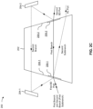
- FIGS. 4 A- 4 B are diagrams of an example cross-over etalon device 400 / 400 ′.
- etalon device 400 / 400 ′ includes an optical component 402 that is a mirror-symmetric rhombus shape with opposing faces 404 - 1 and 404 - 2 .
- Each opposing face includes an upper facet 406 and a lower facet 406 .
- face 404 - 1 includes upper facet 406 - 1 a and lower facet 406 - 1 b
- face 404 - 2 includes upper facet 406 - 2 a and lower facet 406 - 2 b.
- mirrors may be positioned at upper facets 406 - 1 a and 406 - 1 b.
- FIG. 4 B mirrors may be positioned at upper facet 406 - 1 a and lower facet 406 - 2 b. This results in a 4-port device that can be used as an interleaver or compact etalon.
- etalon devices 400 / 400 ′ may be implemented with mirrors or a prism.
- facets of etalon devices 400 / 400 ′ form a resonant cavity.
- ports of etalon device 400 / 400 ′ are located on facets that are partially reflecting surfaces. For example, in FIG. 4 A , lower facets 406 - 1 b and 406 - 2 b are partially reflecting surfaces (and upper facets 406 - 1 a and 406 - 2 a are fully reflecting surfaces).
- FIG. 4 A lower facets 406 - 1 b and 406 - 2 b are partially reflecting surfaces (and upper facets 406 - 1 a and 406 - 2 a are fully reflecting surfaces).
- etalon device 400 / 400 ′ may be configured to receive two input beams, P in (e.g., which may be a Tx beam) and RX in . Further, etalon device 400 / 400 ′ may have two outputs P out and Rx out , and two back reflected beams, Rx out-off-grid and P out-off-grid .
- P in e.g., which may be a Tx beam
- RX in etalon device 400 / 400 ′
- etalon device 400 / 400 ′ may have two outputs P out and Rx out , and two back reflected beams, Rx out-off-grid and P out-off-grid .
- FIGS. 4 A- 4 C are provided as an example. Other examples may differ from what is described with regard to FIGS. 4 A- 4 C .
- satisfying a threshold may, depending on the context, refer to a value being greater than the threshold, greater than or equal to the threshold, less than the threshold, less than or equal to the threshold, equal to the threshold, not equal to the threshold, or the like.
- “at least one of: a, b, or c” is intended to cover a, b, c, a-b, a-c, b-c, and a-b-c, as well as any combination with multiple of the same item.
- the terms “has,” “have,” “having,” or the like are intended to be open-ended terms. Further, the phrase “based on” is intended to mean “based, at least in part, on” unless explicitly stated otherwise. Also, as used herein, the term “or” is intended to be inclusive when used in a series and may be used interchangeably with “and/or,” unless explicitly stated otherwise (e.g., if used in combination with “either” or “only one of”). Further, spatially relative terms, such as “below,” “lower,” “above,” “upper,” and the like, may be used herein for ease of description to describe one element or feature's relationship to another element(s) or feature(s) as illustrated in the figures.
- the spatially relative terms are intended to encompass different orientations of the apparatus, device, and/or element in use or operation in addition to the orientation depicted in the figures.
- the apparatus may be otherwise oriented (rotated 90 degrees or at other orientations) and the spatially relative descriptors used herein may likewise be interpreted accordingly.
Landscapes
- Physics & Mathematics (AREA)
- Engineering & Computer Science (AREA)
- General Physics & Mathematics (AREA)
- Optics & Photonics (AREA)
- Computer Networks & Wireless Communication (AREA)
- Signal Processing (AREA)
- Microelectronics & Electronic Packaging (AREA)
- Electromagnetism (AREA)
- Optical Couplings Of Light Guides (AREA)
Abstract
Description
Claims (20)
Priority Applications (2)
| Application Number | Priority Date | Filing Date | Title |
|---|---|---|---|
| US17/648,765 US12001057B2 (en) | 2021-10-01 | 2022-01-24 | Bidirectional filter |
| US18/731,659 US20240319446A1 (en) | 2021-10-01 | 2024-06-03 | Bidirectional filter |
Applications Claiming Priority (2)
| Application Number | Priority Date | Filing Date | Title |
|---|---|---|---|
| US202163261985P | 2021-10-01 | 2021-10-01 | |
| US17/648,765 US12001057B2 (en) | 2021-10-01 | 2022-01-24 | Bidirectional filter |
Related Child Applications (1)
| Application Number | Title | Priority Date | Filing Date |
|---|---|---|---|
| US18/731,659 Continuation US20240319446A1 (en) | 2021-10-01 | 2024-06-03 | Bidirectional filter |
Publications (2)
| Publication Number | Publication Date |
|---|---|
| US20230106876A1 US20230106876A1 (en) | 2023-04-06 |
| US12001057B2 true US12001057B2 (en) | 2024-06-04 |
Family
ID=85774795
Family Applications (2)
| Application Number | Title | Priority Date | Filing Date |
|---|---|---|---|
| US17/648,765 Active US12001057B2 (en) | 2021-10-01 | 2022-01-24 | Bidirectional filter |
| US18/731,659 Pending US20240319446A1 (en) | 2021-10-01 | 2024-06-03 | Bidirectional filter |
Family Applications After (1)
| Application Number | Title | Priority Date | Filing Date |
|---|---|---|---|
| US18/731,659 Pending US20240319446A1 (en) | 2021-10-01 | 2024-06-03 | Bidirectional filter |
Country Status (1)
| Country | Link |
|---|---|
| US (2) | US12001057B2 (en) |
Citations (14)
| Publication number | Priority date | Publication date | Assignee | Title |
|---|---|---|---|---|
| US6125220A (en) * | 1998-12-23 | 2000-09-26 | Copner; Nigel | Interferometric optical device including a resonant optical cavity |
| US6275322B1 (en) * | 1999-06-08 | 2001-08-14 | Jds Uniphase Corporation | Michelson phase shifter interleaver/deinterleavers |
| US20010040681A1 (en) * | 1998-12-23 | 2001-11-15 | Jds Uniphase Corporation | Interferometric optical device including an optical resonator |
| US6469790B1 (en) * | 1996-10-28 | 2002-10-22 | Christopher J. Manning | Tilt-compensated interferometers |
| US20020154314A1 (en) * | 2001-02-27 | 2002-10-24 | Nigel Copner | Athermal interferometer |
| US20020154313A1 (en) * | 2001-04-23 | 2002-10-24 | Gan Zhou | Optical interferometer for multiplexing optical signals |
| US20020171908A1 (en) * | 2001-02-27 | 2002-11-21 | Jds Uniphase Corporation | Low dispersion interleaver |
| US6785000B2 (en) * | 2002-06-24 | 2004-08-31 | Jds Uniphase Corporation | Bulk optical interferometer |
| US20070070505A1 (en) * | 2004-03-08 | 2007-03-29 | Optoplex Corporation | Michelson interferometer based delay line interferometers |
| US7433054B1 (en) * | 2006-05-18 | 2008-10-07 | Lockheed Martin Corporation | Tunable Michelson and Mach-Zehnder interferometers modified with Gires-Tournois interferometers |
| US8411350B2 (en) * | 2009-11-25 | 2013-04-02 | Huawei Technologies Co., Ltd. | Optical demodulator |
| US8570524B2 (en) * | 2009-08-04 | 2013-10-29 | University Of Florida Research Foundation, Inc. | Stable monolithic interferometer for wavelenghth calibration |
| US20160124146A1 (en) * | 2013-06-24 | 2016-05-05 | Huawei Technologies Co., Ltd | Optical module and optical network system |
| US20190145825A1 (en) * | 2016-06-28 | 2019-05-16 | Oclaro Technology Limited | Optical locker |
Family Cites Families (6)
| Publication number | Priority date | Publication date | Assignee | Title |
|---|---|---|---|---|
| KR100456984B1 (en) * | 2001-03-06 | 2004-11-10 | 가부시끼가이샤 도시바 | Semiconductor laser device |
| US20020176659A1 (en) * | 2001-05-21 | 2002-11-28 | Jds Uniphase Corporation | Dynamically tunable resonator for use in a chromatic dispersion compensator |
| US6690513B2 (en) * | 2001-07-03 | 2004-02-10 | Jds Uniphase Corporation | Rhomb interleaver |
| EP1359691B1 (en) * | 2002-04-30 | 2005-06-08 | Alcatel | Optical interleaver and deinterleaver |
| JP5177969B2 (en) * | 2006-07-12 | 2013-04-10 | 浜松ホトニクス株式会社 | Optical amplifier |
| US8036506B2 (en) * | 2009-03-27 | 2011-10-11 | Lightwaves 2020, Inc. | Multi-fiber section tunable optical filter |
-
2022
- 2022-01-24 US US17/648,765 patent/US12001057B2/en active Active
-
2024
- 2024-06-03 US US18/731,659 patent/US20240319446A1/en active Pending
Patent Citations (14)
| Publication number | Priority date | Publication date | Assignee | Title |
|---|---|---|---|---|
| US6469790B1 (en) * | 1996-10-28 | 2002-10-22 | Christopher J. Manning | Tilt-compensated interferometers |
| US6125220A (en) * | 1998-12-23 | 2000-09-26 | Copner; Nigel | Interferometric optical device including a resonant optical cavity |
| US20010040681A1 (en) * | 1998-12-23 | 2001-11-15 | Jds Uniphase Corporation | Interferometric optical device including an optical resonator |
| US6275322B1 (en) * | 1999-06-08 | 2001-08-14 | Jds Uniphase Corporation | Michelson phase shifter interleaver/deinterleavers |
| US20020171908A1 (en) * | 2001-02-27 | 2002-11-21 | Jds Uniphase Corporation | Low dispersion interleaver |
| US20020154314A1 (en) * | 2001-02-27 | 2002-10-24 | Nigel Copner | Athermal interferometer |
| US20020154313A1 (en) * | 2001-04-23 | 2002-10-24 | Gan Zhou | Optical interferometer for multiplexing optical signals |
| US6785000B2 (en) * | 2002-06-24 | 2004-08-31 | Jds Uniphase Corporation | Bulk optical interferometer |
| US20070070505A1 (en) * | 2004-03-08 | 2007-03-29 | Optoplex Corporation | Michelson interferometer based delay line interferometers |
| US7433054B1 (en) * | 2006-05-18 | 2008-10-07 | Lockheed Martin Corporation | Tunable Michelson and Mach-Zehnder interferometers modified with Gires-Tournois interferometers |
| US8570524B2 (en) * | 2009-08-04 | 2013-10-29 | University Of Florida Research Foundation, Inc. | Stable monolithic interferometer for wavelenghth calibration |
| US8411350B2 (en) * | 2009-11-25 | 2013-04-02 | Huawei Technologies Co., Ltd. | Optical demodulator |
| US20160124146A1 (en) * | 2013-06-24 | 2016-05-05 | Huawei Technologies Co., Ltd | Optical module and optical network system |
| US20190145825A1 (en) * | 2016-06-28 | 2019-05-16 | Oclaro Technology Limited | Optical locker |
Also Published As
| Publication number | Publication date |
|---|---|
| US20240319446A1 (en) | 2024-09-26 |
| US20230106876A1 (en) | 2023-04-06 |
Similar Documents
| Publication | Publication Date | Title |
|---|---|---|
| US6690513B2 (en) | Rhomb interleaver | |
| US6765679B2 (en) | Multi-cavity interferometer with dispersion compensating resonators | |
| US6907167B2 (en) | Optical interleaving with enhanced spectral response and reduced polarization sensitivity | |
| US7173763B2 (en) | Optical interleaver and filter cell design with enhanced clear aperture | |
| JP6452900B2 (en) | Optical components and optical modules | |
| US20090225428A1 (en) | Optical module | |
| US6694066B2 (en) | Method and apparatus for an optical filter | |
| US6871022B2 (en) | Cascaded optical multiplexer | |
| US6684002B2 (en) | Method and apparatus for an optical filter | |
| US12001057B2 (en) | Bidirectional filter | |
| US7262904B1 (en) | Tunable optical add/drop device | |
| US6850364B2 (en) | Method and apparatus for an optical multiplexer and demultiplexer with an optical processing loop | |
| US7050671B1 (en) | Tunable compensation of chromatic dispersion using etalons with tunable optical path length and non-tunable reflectivity | |
| US6185040B1 (en) | Virtually imaged phased array (VIPA) having spacer element and optical length adjusting element | |
| US7268944B2 (en) | Optical interleaver, filter cell, and component design with reduced chromatic dispersion | |
| US6577398B1 (en) | Resonant optical cavity | |
| KR20050028814A (en) | Wavelength division multiplexer | |
| US20030099019A1 (en) | Compensation of chromatic dispersion using cascaded etalons of variable reflectivity | |
| US11909437B2 (en) | Optic for multi-pass optical channel monitor | |
| US20230017729A1 (en) | Compact etalon structure | |
| US6768591B2 (en) | Interleaver | |
| US20030231824A1 (en) | Tunable dispersion compensators | |
| JPH07198937A (en) | Wavelength tuning narrow band interference filter module | |
| US20040227996A1 (en) | Optical interleaver and filter cell design with enhanced thermal stability | |
| US20040223222A1 (en) | Hermetically sealed collimator and optical interleaver design |
Legal Events
| Date | Code | Title | Description |
|---|---|---|---|
| FEPP | Fee payment procedure |
Free format text: ENTITY STATUS SET TO UNDISCOUNTED (ORIGINAL EVENT CODE: BIG.); ENTITY STATUS OF PATENT OWNER: LARGE ENTITY |
|
| AS | Assignment |
Owner name: LUMENTUM OPERATIONS LLC, CALIFORNIA Free format text: ASSIGNMENT OF ASSIGNORS INTEREST;ASSIGNOR:JANSSEN, ADRIAN PERRIN;REEL/FRAME:061893/0491 Effective date: 20220214 Owner name: LUMENTUM OPERATIONS LLC, CALIFORNIA Free format text: ASSIGNMENT OF ASSIGNOR'S INTEREST;ASSIGNOR:JANSSEN, ADRIAN PERRIN;REEL/FRAME:061893/0491 Effective date: 20220214 |
|
| STPP | Information on status: patent application and granting procedure in general |
Free format text: NON FINAL ACTION MAILED |
|
| STPP | Information on status: patent application and granting procedure in general |
Free format text: RESPONSE TO NON-FINAL OFFICE ACTION ENTERED AND FORWARDED TO EXAMINER |
|
| STPP | Information on status: patent application and granting procedure in general |
Free format text: FINAL REJECTION MAILED |
|
| STPP | Information on status: patent application and granting procedure in general |
Free format text: RESPONSE AFTER FINAL ACTION FORWARDED TO EXAMINER |
|
| STPP | Information on status: patent application and granting procedure in general |
Free format text: ADVISORY ACTION MAILED |
|
| STPP | Information on status: patent application and granting procedure in general |
Free format text: DOCKETED NEW CASE - READY FOR EXAMINATION |
|
| STPP | Information on status: patent application and granting procedure in general |
Free format text: NOTICE OF ALLOWANCE MAILED -- APPLICATION RECEIVED IN OFFICE OF PUBLICATIONS |
|
| STPP | Information on status: patent application and granting procedure in general |
Free format text: AWAITING TC RESP., ISSUE FEE NOT PAID |
|
| STPP | Information on status: patent application and granting procedure in general |
Free format text: NOTICE OF ALLOWANCE MAILED -- APPLICATION RECEIVED IN OFFICE OF PUBLICATIONS |
|
| STPP | Information on status: patent application and granting procedure in general |
Free format text: PUBLICATIONS -- ISSUE FEE PAYMENT VERIFIED |
|
| STCF | Information on status: patent grant |
Free format text: PATENTED CASE |