US11973133B2 - High electron mobility transistor and method for fabricating the same - Google Patents
High electron mobility transistor and method for fabricating the same Download PDFInfo
- Publication number
- US11973133B2 US11973133B2 US18/144,822 US202318144822A US11973133B2 US 11973133 B2 US11973133 B2 US 11973133B2 US 202318144822 A US202318144822 A US 202318144822A US 11973133 B2 US11973133 B2 US 11973133B2
- Authority
- US
- United States
- Prior art keywords
- region
- hemt
- layer
- electrode
- hard mask
- Prior art date
- Legal status (The legal status is an assumption and is not a legal conclusion. Google has not performed a legal analysis and makes no representation as to the accuracy of the status listed.)
- Active
Links
Images


Classifications
-
- H01L29/778—
-
- H01L27/0629—
-
- H01L29/0649—
-
- H01L29/2003—
-
- H01L29/66462—
-
- H—ELECTRICITY
- H10—SEMICONDUCTOR DEVICES; ELECTRIC SOLID-STATE DEVICES NOT OTHERWISE PROVIDED FOR
- H10D—INORGANIC ELECTRIC SEMICONDUCTOR DEVICES
- H10D30/00—Field-effect transistors [FET]
- H10D30/01—Manufacture or treatment
- H10D30/015—Manufacture or treatment of FETs having heterojunction interface channels or heterojunction gate electrodes, e.g. HEMT
-
- H—ELECTRICITY
- H10—SEMICONDUCTOR DEVICES; ELECTRIC SOLID-STATE DEVICES NOT OTHERWISE PROVIDED FOR
- H10D—INORGANIC ELECTRIC SEMICONDUCTOR DEVICES
- H10D30/00—Field-effect transistors [FET]
- H10D30/40—FETs having zero-dimensional [0D], one-dimensional [1D] or two-dimensional [2D] charge carrier gas channels
- H10D30/47—FETs having zero-dimensional [0D], one-dimensional [1D] or two-dimensional [2D] charge carrier gas channels having two-dimensional [2D] charge carrier gas channels, e.g. nanoribbon FETs or high electron mobility transistors [HEMT]
-
- H—ELECTRICITY
- H10—SEMICONDUCTOR DEVICES; ELECTRIC SOLID-STATE DEVICES NOT OTHERWISE PROVIDED FOR
- H10D—INORGANIC ELECTRIC SEMICONDUCTOR DEVICES
- H10D62/00—Semiconductor bodies, or regions thereof, of devices having potential barriers
- H10D62/10—Shapes, relative sizes or dispositions of the regions of the semiconductor bodies; Shapes of the semiconductor bodies
- H10D62/113—Isolations within a component, i.e. internal isolations
- H10D62/115—Dielectric isolations, e.g. air gaps
-
- H—ELECTRICITY
- H10—SEMICONDUCTOR DEVICES; ELECTRIC SOLID-STATE DEVICES NOT OTHERWISE PROVIDED FOR
- H10D—INORGANIC ELECTRIC SEMICONDUCTOR DEVICES
- H10D62/00—Semiconductor bodies, or regions thereof, of devices having potential barriers
- H10D62/80—Semiconductor bodies, or regions thereof, of devices having potential barriers characterised by the materials
- H10D62/85—Semiconductor bodies, or regions thereof, of devices having potential barriers characterised by the materials being Group III-V materials, e.g. GaAs
- H10D62/8503—Nitride Group III-V materials, e.g. AlN or GaN
-
- H—ELECTRICITY
- H10—SEMICONDUCTOR DEVICES; ELECTRIC SOLID-STATE DEVICES NOT OTHERWISE PROVIDED FOR
- H10D—INORGANIC ELECTRIC SEMICONDUCTOR DEVICES
- H10D84/00—Integrated devices formed in or on semiconductor substrates that comprise only semiconducting layers, e.g. on Si wafers or on GaAs-on-Si wafers
- H10D84/01—Manufacture or treatment
- H10D84/02—Manufacture or treatment characterised by using material-based technologies
- H10D84/05—Manufacture or treatment characterised by using material-based technologies using Group III-V technology
-
- H—ELECTRICITY
- H10—SEMICONDUCTOR DEVICES; ELECTRIC SOLID-STATE DEVICES NOT OTHERWISE PROVIDED FOR
- H10D—INORGANIC ELECTRIC SEMICONDUCTOR DEVICES
- H10D84/00—Integrated devices formed in or on semiconductor substrates that comprise only semiconducting layers, e.g. on Si wafers or on GaAs-on-Si wafers
- H10D84/80—Integrated devices formed in or on semiconductor substrates that comprise only semiconducting layers, e.g. on Si wafers or on GaAs-on-Si wafers characterised by the integration of at least one component covered by groups H10D12/00 or H10D30/00, e.g. integration of IGFETs
- H10D84/811—Combinations of field-effect devices and one or more diodes, capacitors or resistors
-
- H—ELECTRICITY
- H10—SEMICONDUCTOR DEVICES; ELECTRIC SOLID-STATE DEVICES NOT OTHERWISE PROVIDED FOR
- H10D—INORGANIC ELECTRIC SEMICONDUCTOR DEVICES
- H10D1/00—Resistors, capacitors or inductors
- H10D1/60—Capacitors
- H10D1/68—Capacitors having no potential barriers
-
- H—ELECTRICITY
- H10—SEMICONDUCTOR DEVICES; ELECTRIC SOLID-STATE DEVICES NOT OTHERWISE PROVIDED FOR
- H10D—INORGANIC ELECTRIC SEMICONDUCTOR DEVICES
- H10D30/00—Field-effect transistors [FET]
- H10D30/40—FETs having zero-dimensional [0D], one-dimensional [1D] or two-dimensional [2D] charge carrier gas channels
- H10D30/47—FETs having zero-dimensional [0D], one-dimensional [1D] or two-dimensional [2D] charge carrier gas channels having two-dimensional [2D] charge carrier gas channels, e.g. nanoribbon FETs or high electron mobility transistors [HEMT]
- H10D30/471—High electron mobility transistors [HEMT] or high hole mobility transistors [HHMT]
- H10D30/475—High electron mobility transistors [HEMT] or high hole mobility transistors [HHMT] having wider bandgap layer formed on top of lower bandgap active layer, e.g. undoped barrier HEMTs such as i-AlGaN/GaN HEMTs
-
- H—ELECTRICITY
- H10—SEMICONDUCTOR DEVICES; ELECTRIC SOLID-STATE DEVICES NOT OTHERWISE PROVIDED FOR
- H10D—INORGANIC ELECTRIC SEMICONDUCTOR DEVICES
- H10D62/00—Semiconductor bodies, or regions thereof, of devices having potential barriers
- H10D62/10—Shapes, relative sizes or dispositions of the regions of the semiconductor bodies; Shapes of the semiconductor bodies
- H10D62/17—Semiconductor regions connected to electrodes not carrying current to be rectified, amplified or switched, e.g. channel regions
- H10D62/343—Gate regions of field-effect devices having PN junction gates
-
- H—ELECTRICITY
- H10—SEMICONDUCTOR DEVICES; ELECTRIC SOLID-STATE DEVICES NOT OTHERWISE PROVIDED FOR
- H10D—INORGANIC ELECTRIC SEMICONDUCTOR DEVICES
- H10D64/00—Electrodes of devices having potential barriers
- H10D64/20—Electrodes characterised by their shapes, relative sizes or dispositions
- H10D64/23—Electrodes carrying the current to be rectified, amplified, oscillated or switched, e.g. sources, drains, anodes or cathodes
- H10D64/251—Source or drain electrodes for field-effect devices
- H10D64/256—Source or drain electrodes for field-effect devices for lateral devices wherein the source or drain electrodes are recessed in semiconductor bodies
Definitions
- the invention relates to a semiconductor device, and more particularly to a semiconductor device having integrated a high electron mobility transistor (HEMT) and a capacitor.
- HEMT high electron mobility transistor
- High electron mobility transistor (HEMT) fabricated from GaN-based materials have various advantages in electrical, mechanical, and chemical aspects of the field. For instance, advantages including wide band gap, high break down voltage, high electron mobility, high elastic modulus, high piezoelectric and piezoresistive coefficients, and chemical inertness. All of these advantages allow GaN-based materials to be used in numerous applications including high intensity light emitting diodes (LEDs), power switching devices, regulators, battery protectors, display panel drivers, and communication devices.
- LEDs high intensity light emitting diodes
- a semiconductor device includes a substrate having a high electron mobility transistor (HEMT) region and a capacitor region, a first mesa isolation on the HEMT region, a HEMT on the first mesa isolation, a second mesa isolation on the capacitor region, and a capacitor on the second mesa isolation.
- the semiconductor device further includes buffer layer between the substrate, the first mesa isolation, and the second mesa isolation, in which bottom surfaces of the first mesa isolation and the second mesa isolation are coplanar.
- HEMT high electron mobility transistor
- a semiconductor device includes a substrate having a high electron mobility transistor (HEMT) region and a capacitor region, a mesa isolation on the HEMT region, a HEMT on the mesa isolation, a capacitor on the capacitor region, and a buffer layer between the mesa isolation, the capacitor, and substrate.
- HEMT high electron mobility transistor
- a semiconductor device includes a substrate having a high electron mobility transistor (HEMT) region and a capacitor region, a mesa isolation on the HEMT region, a HEMT on the mesa isolation, a hard mask around the HEMT and extending to the capacitor region, and a capacitor on the hard mask.
- HEMT high electron mobility transistor
- FIGS. 1 - 3 illustrate a method for fabricating a HEMT according to an embodiment of the present invention.
- FIGS. 4 - 6 illustrate a method for fabricating a HEMT according to an embodiment of the present invention.
- FIGS. 7 - 9 illustrate a method for fabricating a HEMT according to an embodiment of the present invention.
- FIGS. 1 - 3 illustrate a method for fabricating a HEMT according to an embodiment of the present invention.
- a substrate 12 such as a substrate made from silicon, silicon carbide, or aluminum oxide (or also referred to as sapphire) is provided, in which the substrate 12 could be a single-layered substrate, a multi-layered substrate, gradient substrate, or combination thereof.
- the substrate 12 could also include a silicon-on-insulator (SOI) substrate.
- SOI silicon-on-insulator
- the buffer layer 18 is preferably made of III-V semiconductors such as gallium nitride (GaN), in which a thickness of the buffer layer 18 could be between 0.5 microns to 10 microns.
- the formation of the buffer layer 18 could be accomplished by a molecular-beam epitaxy (MBE) process, a metal organic chemical vapor deposition (MOCVD) process, a chemical vapor deposition (CVD) process, a hydride vapor phase epitaxy (HVPE) process, or combination thereof.
- MBE molecular-beam epitaxy
- MOCVD metal organic chemical vapor deposition
- CVD chemical vapor deposition
- HVPE hydride vapor phase epitaxy
- the barrier layer 20 is preferably made of III-V semiconductor such as aluminum gallium nitride (Al x Ga 1-x N), in which 0 ⁇ x ⁇ 1, x being less than or equal to 20%, and the barrier layer 20 preferably includes an epitaxial layer formed through epitaxial growth process. Similar to the buffer layer 18 , the formation of the barrier layer 20 on the buffer layer 18 could be accomplished by a molecular-beam epitaxy (MBE) process, a metal organic chemical vapor deposition (MOCVD) process, a chemical vapor deposition (CVD) process, a hydride vapor phase epitaxy (HVPE) process, or combination thereof.
- MBE molecular-beam epitaxy
- MOCVD metal organic chemical vapor deposition
- CVD chemical vapor deposition
- HVPE hydride vapor phase epitaxy
- barrier layer 20 is formed directly on the surface of the buffer layer 18 , according to another embodiment of the present invention, it would also be desirable to form an extra metal nitride layer (not shown) including but not limited to for example aluminum nitride (AlN) between the buffer layer 18 and the barrier layer 20 , which is also within the scope of the present invention.
- AlN aluminum nitride
- the p-type semiconductor layer 22 preferably is a III-V compound layer including p-type GaN (p-GaN) and the formation of the p-type semiconductor layer 22 on the surface of the barrier layer 20 could be accomplished by a molecular-beam epitaxy (MBE) process, a metal organic chemical vapor deposition (MOCVD) process, a chemical vapor deposition (CVD) process, a hydride vapor phase epitaxy (HVPE) process, or combination thereof.
- MBE molecular-beam epitaxy
- MOCVD metal organic chemical vapor deposition
- CVD chemical vapor deposition
- HVPE hydride vapor phase epitaxy
- a MESA isolation process is conducted to form mesa isolations 24 , 26 on the HEMT region 14 and capacitor region 16 respectively so that devices could be isolated to operate independently without affecting each other.
- the MESA isolation process could be accomplished by conducting a photo-etching process to remove part of p-type semiconductor layer 22 , part of the barrier layer 20 , and part of the buffer layer 18 , in which the patterned p-type semiconductor layer 22 , the patterned barrier layer 20 , and the patterned buffer layer 18 preferably share equal widths and edges of the three layers are aligned.
- the width of the remaining un-patterned buffer layer 18 is preferably equal to the width of the substrate 12 .
- each of the mesa isolations 24 , 26 includes a patterned buffer layer 18 , in which the thickness of the patterned buffer layer 18 is approximately 300 nm, the thickness of the patterned barrier layer 20 is approximately 10 nm, and the thickness of the patterned p-type semiconductor layer 22 is approximately 100 nm.
- a photo-etching process is conducted to remove part of the p-type semiconductor layer 22 on the HEMT region 14 and all of the p-type semiconductor layer 22 on the capacitor region 16 so that the remaining p-type semiconductor layer 22 is only disposed on the barrier layer 20 on HEMT region 14 while none of the p-type semiconductor layer 22 is remained on the surface of the barrier layer 20 on capacitor region 16 , in which the patterned p-type semiconductor layer 22 preferably serves as part of the gate structure for the HEMT device in the later process.
- a hard mask 28 is conformally formed on the buffer layer 18 to cover the mesa isolations 24 , 26 on the HEMT region 14 and the capacitor region 16 .
- the hard mask 28 preferably includes silicon nitride and the thickness of the hard mask 28 is approximately 200 nm, but not limited thereto.
- one or more photo-etching process is conducted to remove part of the hard mask 28 and part of the barrier layer 20 on the HEMT region 14 for forming a plurality of recesses (not shown), a conductive material is formed into the recesses and on the surface of the hard mask 28 on both HEMT region 14 and capacitor region 16 , and a pattern transfer process is conducted to remove part of the conductive material.
- the conductive material deposited into the recesses on the HEMT region 14 serves as a source electrode 30 and drain electrode 32
- the conductive material disposed on the source electrode 30 and drain electrode 32 and extended to the surface of the hard mask 28 adjacent to two sides of the source electrode 30 and drain electrode 32 serves as a source electrode extension 34 and drain electrode extension 36
- the conductive material being patterned on the surface of the hard mask 28 on the capacitor region 16 preferably serves as a bottom electrode 38 for the capacitor.
- another hard mask 40 is formed on the surface of hard mask 28 on the HEMT region 14 and extending to the bottom electrode 38 on the capacitor region 16 , in which the hard mask 40 on the capacitor region 16 preferably serves as a capacitor dielectric layer 42 .
- the thickness of the capacitor dielectric layer 42 is between 20-100 nm, but not limited thereto.
- one or more photo-etching process is conducted to remove part of the hard mask 40 and part of the hard mask 28 on the HEMT region 14 for forming a recess exposing the p-type semiconductor layer 22
- another conductive material is formed on the hard mask 40 on HEMT region 14 to fill the recess completely while covering the surface of the hard mask 40 on the capacitor region 16
- a pattern transfer process is conducted to remove part of the conductive material, in which the conductive material deposited into the recess and part of the conductive material on the surface of the hard mask 40 on the HEMT region 14 preferably serves as a gate electrode 44 while the patterned conductive material layer on the capacitor region 16 serves as a top electrode for the capacitor.
- the gate electrode 44 , source electrode 30 , and drain electrode 32 are preferably made of metal, in which gate electrode 44 preferably includes Schottky metal while the source electrode 30 and the drain electrode 32 are preferably made of ohmic contact metals.
- each of the gate electrode 44 , source electrode 30 , and drain electrode 32 could include gold (Au), silver (Ag), platinum (Pt), titanium (Ti), aluminum (Al), tungsten (W), palladium (Pd), or combination thereof.
- a contact plug formation could be conducted to form contact plugs 50 electrically connected to the gate electrode 44 , source electrode 30 , and drain electrode 32 on the HMET region 14 and the bottom electrode 38 and top electrode 46 on the capacitor region 16 .
- the formation of contact plugs 50 could be accomplished by first forming an interlayer dielectric (ILD) layer 48 on the hard mask 40 on both HEMT region 14 and capacitor region 16 , removing part of the ILD layer 48 and part of the hard mask 40 to form contact holes (not shown), and then depositing a barrier layer (not shown) and a metal layer (not shown) into the contact holes.
- ILD interlayer dielectric
- a planarizing process such as chemical mechanical polishing (CMP) process is then conducted to remove part of the metal layer, part of the barrier layer, and even part of the ILD layer 48 to form contact plugs 50 in the contact holes, in which the top surface of the contact plugs 50 is even with the top surface of the ILD layer 48 .
- the barrier layer is selected from the group consisting of Ti, Ta, TiN, TaN, and WN and the metal layer is selected from the group consisting of Al, Ti, Ta, W, Nb, Mo, and Cu.
- FIG. 3 further illustrates a structural view of a semiconductor device according to an embodiment of the present invention.
- the semiconductor device preferably includes a HEMT region 14 and a capacitor region 16 defined on the substrate 12 , a mesa isolation 24 disposed on the HEMT region 14 , a HEMT 52 disposed on the mesa isolation 24 , another mesa isolation 26 disposed on the capacitor region 16 , a buffer layer 18 disposed on the substrate 12 and between the mesa isolations 24 , 26 , and a capacitor 54 disposed on the mesa isolation 26 , in which the bottom surfaces of the mesa isolations 24 , 26 are coplanar and both mesa isolations 24 , 26 includes GaN.
- the HEMT 52 includes a barrier layer 20 disposed on the mesa isolation 24 , a p-type semiconductor layer 22 disposed on the barrier layer 20 , a gate electrode 44 disposed on the p-type semiconductor layer 22 , a source electrode 30 and drain electrode 32 adjacent to two sides of the gate electrode 44 , a source electrode extension 34 disposed on the source electrode 30 , a drain electrode extension 36 disposed on the drain electrode 32 , and a hard mask 28 disposed on the mesa isolations 24 , 26 and surrounding the source electrode 30 and drain electrode 32 .
- the capacitor 54 includes a bottom electrode 38 disposed on the hard mask 28 , a capacitor dielectric layer 42 disposed on the bottom electrode 38 and extending to the top surface and sidewall of the hard mask 28 on the HEMT region 14 , and a top electrode 46 disposed on the capacitor dielectric layer 42 , in which the bottom surface of the bottom electrode 38 is even with the bottom surface of the source electrode extension 34 while the top surface of the top electrode 46 is even with the top surface of the gate electrode 44 .
- FIGS. 4 - 6 illustrate a method for fabricating a HEMT according to an embodiment of the present invention.
- a substrate 12 such as a substrate made from silicon, silicon carbide, or aluminum oxide (or also referred to as sapphire) is provided, in which the substrate 12 could be a single-layered substrate, a multi-layered substrate, gradient substrate, or combination thereof.
- the substrate 12 could also include a silicon-on-insulator (SOI) substrate.
- SOI silicon-on-insulator
- the buffer layer 18 is preferably made of III-V semiconductors such as gallium nitride (GaN), in which a thickness of the buffer layer 18 could be between 0.5 microns to 10 microns.
- the formation of the buffer layer 18 could be accomplished by a molecular-beam epitaxy (MBE) process, a metal organic chemical vapor deposition (MOCVD) process, a chemical vapor deposition (CVD) process, a hydride vapor phase epitaxy (HVPE) process, or combination thereof.
- MBE molecular-beam epitaxy
- MOCVD metal organic chemical vapor deposition
- CVD chemical vapor deposition
- HVPE hydride vapor phase epitaxy
- the barrier layer 20 is preferably made of III-V semiconductor such as aluminum gallium nitride (Al x Ga 1-x N), in which 0 ⁇ x ⁇ 1, x being less than or equal to 20%, and the barrier layer 20 preferably includes an epitaxial layer formed through epitaxial growth process. Similar to the buffer layer 18 , the formation of the barrier layer 20 on the buffer layer 18 could be accomplished by a molecular-beam epitaxy (MBE) process, a metal organic chemical vapor deposition (MOCVD) process, a chemical vapor deposition (CVD) process, a hydride vapor phase epitaxy (HVPE) process, or combination thereof.
- MBE molecular-beam epitaxy
- MOCVD metal organic chemical vapor deposition
- CVD chemical vapor deposition
- HVPE hydride vapor phase epitaxy
- barrier layer 20 is formed directly on the surface of the buffer layer 18 , according to another embodiment of the present invention, it would also be desirable to form an extra metal nitride layer (not shown) including but not limited to for example aluminum nitride (AlN) between the buffer layer 18 and the barrier layer 20 , which is also within the scope of the present invention.
- AlN aluminum nitride
- the p-type semiconductor layer 22 preferably is a III-V compound layer including p-type GaN (p-GaN) and the formation of the p-type semiconductor layer 22 on the surface of the barrier layer 20 could be accomplished by a molecular-beam epitaxy (MBE) process, a metal organic chemical vapor deposition (MOCVD) process, a chemical vapor deposition (CVD) process, a hydride vapor phase epitaxy (HVPE) process, or combination thereof.
- MBE molecular-beam epitaxy
- MOCVD metal organic chemical vapor deposition
- CVD chemical vapor deposition
- HVPE hydride vapor phase epitaxy
- a MESA isolation process is conducted to form a mesa isolation 24 on the HEMT region 14 .
- the MESA isolation process could be accomplished by conducting a photo-etching process to remove part of p-type semiconductor layer 22 , part of the barrier layer 20 , and part of the buffer layer 18 , in which the patterned p-type semiconductor layer 22 , the patterned barrier layer 20 , and the patterned buffer layer 18 preferably share equal widths and edges of the three layers are aligned.
- the width of the remaining un-patterned buffer layer 18 is preferably equal to the width of the substrate 12 .
- the mesa isolation 24 includes a patterned buffer layer 18 , in which the thickness of the patterned buffer layer 18 is approximately 300 nm, the thickness of the patterned barrier layer 20 is approximately 10 nm, and the thickness of the patterned p-type semiconductor layer 22 is approximately 100 nm.
- a photo-etching process is conducted to remove part of the p-type semiconductor layer 22 on the HEMT region 14 , in which the patterned p-type semiconductor layer 22 preferably serves as part of the gate structure for the HEMT device in the later process.
- a hard mask 28 is conformally formed on the buffer layer 18 to cover the mesa isolation 24 on the HEMT region 14 while extending to the buffer layer 18 on the capacitor region 16 .
- the hard mask 28 preferably includes silicon nitride and the thickness of the hard mask 28 is approximately 200 nm, but not limited thereto.
- one or more photo-etching process is conducted to remove part of the hard mask 28 and part of the barrier layer 20 on the HEMT region 14 and majority of the hard mask 28 on the capacitor region 16 for forming a plurality of recesses (not shown), a conductive material is formed into the recesses on both HEMT region 14 and capacitor region 16 , and a pattern transfer process is conducted to remove part of the conductive material.
- the conductive material deposited into the recesses on the HEMT region 14 serves as a source electrode 30 and drain electrode 32
- the conductive material disposed on the source electrode 30 and drain electrode 32 and extended to the surface of the hard mask 28 adjacent to two sides of the source electrode 30 and drain electrode 32 serves as a source electrode extension 34 and drain electrode extension 36
- the conductive material being formed into the recess or trench on the capacitor region 16 preferably serves as a bottom electrode 38 for the capacitor.
- another hard mask 40 is formed on the surface of hard mask 28 on the HEMT region 14 and extending to the bottom electrode 38 on the capacitor region 16 , in which the hard mask 40 on the capacitor region 16 preferably serves as a capacitor dielectric layer 42 .
- the thickness of the capacitor dielectric layer 42 is between 20-100 nm, but not limited thereto.
- one or more photo-etching process is conducted to remove part of the hard mask 40 and part of the hard mask 28 on the HEMT region 14 for forming a recess exposing the p-type semiconductor layer 22
- another conductive material is formed on the hard mask 40 on HEMT region 14 to fill the recess completely while covering the surface of the hard mask 40 on the capacitor region 16
- a pattern transfer process is conducted to remove part of the conductive material, in which the conductive material deposited into the recess and part of the conductive material on the surface of the hard mask 40 on the HEMT region 14 preferably serves as a T-shape gate electrode 44 while the patterned conductive material layer on the capacitor region 16 serves as a top electrode 46 for the capacitor.
- the gate electrode 44 , source electrode 30 , and drain electrode 32 are preferably made of metal, in which gate electrode 44 preferably includes Schottky metal while the source electrode 30 and the drain electrode 32 are preferably made of ohmic contact metals.
- each of the gate electrode 44 , source electrode 30 , and drain electrode 32 could include gold (Au), silver (Ag), platinum (Pt), titanium (Ti), aluminum (Al), tungsten (W), palladium (Pd), or combination thereof.
- a contact plug formation could be conducted to form contact plugs 50 electrically connected to the gate electrode 44 , source electrode 30 , and drain electrode 32 on the HMET region 14 and the bottom electrode 38 and top electrode 46 on the capacitor region 16 .
- the formation of contact plugs 50 could be accomplished by first forming an interlayer dielectric (ILD) layer 48 on the hard mask 40 on both HEMT region 14 and capacitor region 16 , removing part of the ILD layer 48 and part of the hard mask 40 to form contact holes (not shown), and then depositing a barrier layer (not shown) and a metal layer (not shown) into the contact holes.
- ILD interlayer dielectric
- a planarizing process such as chemical mechanical polishing (CMP) process is then conducted to remove part of the metal layer, part of the barrier layer, and even part of the ILD layer 48 to form contact plugs 50 in the contact holes, in which the top surface of the contact plugs 50 is even with the top surface of the ILD layer 48 .
- the barrier layer is selected from the group consisting of Ti, Ta, TiN, TaN, and WN and the metal layer is selected from the group consisting of Al, Ti, Ta, W, Nb, Mo, and Cu.
- FIG. 6 further illustrates a structural view of a semiconductor device according to an embodiment of the present invention.
- the semiconductor device preferably includes a HEMT region 14 and a capacitor region 16 defined on the substrate 12 , a mesa isolation 24 disposed on the HEMT region 14 , a HEMT 52 disposed on the mesa isolation 24 , a capacitor 54 disposed on the capacitor region 16 , and a buffer layer 18 disposed between the mesa isolation 24 , the capacitor 54 , and the substrate 12 , in which the mesa isolation 24 and the buffer layer 18 both include GaN.
- the HEMT 52 includes a barrier layer 20 disposed on the mesa isolation 24 , a p-type semiconductor layer 22 disposed on the barrier layer 20 , a gate electrode 44 disposed on the p-type semiconductor layer 22 , a source electrode 30 and drain electrode 32 adjacent to two sides of the gate electrode 44 , a source electrode extension 34 disposed on the source electrode 30 , a drain electrode extension 36 disposed on the drain electrode 32 , and a hard mask 28 disposed on the mesa isolation 24 and surrounding the source electrode 30 and drain electrode 32 .
- the capacitor 54 on the other hand includes a bottom electrode 38 disposed on the hard mask 28 , a capacitor dielectric layer 42 disposed on the bottom electrode 38 while extending to the top surface and sidewall of the hard mask 28 on the HEMT region 14 , and a top electrode 46 disposed on the capacitor dielectric layer 42 .
- a mesa isolation 24 is disposed on the HEMT region 14 in this embodiment while the capacitor region 16 includes no mesa isolation so that the bottom electrode 38 would contact the top surface of the buffer layer 18 directly while having a T-shape cross-section.
- the overall thickness of the bottom electrode 38 is substantially equal to the combined thickness of the source electrode 30 and source electrode extension 34 or the combined thickness of the drain electrode 32 and drain electrode extension 36 on the HEMT region 14 .
- the overall thickness of the bottom electrode 38 is about 300 nm
- the thickness of the capacitor dielectric layer 42 is between 20-100 nm
- the thickness of the top electrode 46 is about 100 nm.
- FIGS. 7 - 9 illustrate a method for fabricating a HEMT according to an embodiment of the present invention.
- a substrate 12 such as a substrate made from silicon, silicon carbide, or aluminum oxide (or also referred to as sapphire) is provided, in which the substrate 12 could be a single-layered substrate, a multi-layered substrate, gradient substrate, or combination thereof.
- the substrate 12 could also include a silicon-on-insulator (SOI) substrate.
- SOI silicon-on-insulator
- the buffer layer 18 is preferably made of III-V semiconductors such as gallium nitride (GaN), in which a thickness of the buffer layer 18 could be between 0.5 microns to 10 microns.
- the formation of the buffer layer 18 could be accomplished by a molecular-beam epitaxy (MBE) process, a metal organic chemical vapor deposition (MOCVD) process, a chemical vapor deposition (CVD) process, a hydride vapor phase epitaxy (HVPE) process, or combination thereof.
- MBE molecular-beam epitaxy
- MOCVD metal organic chemical vapor deposition
- CVD chemical vapor deposition
- HVPE hydride vapor phase epitaxy
- the barrier layer 20 is preferably made of III-V semiconductor such as aluminum gallium nitride (Al x Ga 1-x N), in which 0 ⁇ x ⁇ 1, x being less than or equal to 20%, and the barrier layer 20 preferably includes an epitaxial layer formed through epitaxial growth process. Similar to the buffer layer 18 , the formation of the barrier layer 20 on the buffer layer 18 could be accomplished by a molecular-beam epitaxy (MBE) process, a metal organic chemical vapor deposition (MOCVD) process, a chemical vapor deposition (CVD) process, a hydride vapor phase epitaxy (HVPE) process, or combination thereof.
- MBE molecular-beam epitaxy
- MOCVD metal organic chemical vapor deposition
- CVD chemical vapor deposition
- HVPE hydride vapor phase epitaxy
- barrier layer 20 is formed directly on the surface of the buffer layer 18 , according to another embodiment of the present invention, it would also be desirable to form an extra metal nitride layer (not shown) including but not limited to for example aluminum nitride (AlN) between the buffer layer 18 and the barrier layer 20 , which is also within the scope of the present invention.
- AlN aluminum nitride
- the p-type semiconductor layer 22 preferably is a III-V compound layer including p-type GaN (p-GaN) and the formation of the p-type semiconductor layer 22 on the surface of the barrier layer 20 could be accomplished by a molecular-beam epitaxy (MBE) process, a metal organic chemical vapor deposition (MOCVD) process, a chemical vapor deposition (CVD) process, a hydride vapor phase epitaxy (HVPE) process, or combination thereof.
- MBE molecular-beam epitaxy
- MOCVD metal organic chemical vapor deposition
- CVD chemical vapor deposition
- HVPE hydride vapor phase epitaxy
- a MESA isolation process is conducted to form a mesa isolation 24 on the HEMT region 14 .
- the MESA isolation process could be accomplished by conducting a photo-etching process to remove part of p-type semiconductor layer 22 , part of the barrier layer 20 , and part of the buffer layer 18 , in which the patterned p-type semiconductor layer 22 , the patterned barrier layer 20 , and the patterned buffer layer 18 preferably share equal widths and edges of the three layers are aligned.
- the width of the remaining un-patterned buffer layer 18 is preferably equal to the width of the substrate 12 .
- the mesa isolation 24 includes a patterned buffer layer 18 , in which the thickness of the patterned buffer layer 18 is approximately 300 nm, the thickness of the patterned barrier layer 20 is approximately 10 nm, and the thickness of the patterned p-type semiconductor layer 22 is approximately 100 nm.
- a photo-etching process is conducted to remove part of the p-type semiconductor layer 22 on the HEMT region 14 , in which the patterned p-type semiconductor layer 22 preferably serves as part of the gate structure for the HEMT device in the later process.
- a hard mask 28 is conformally formed on the buffer layer 18 to cover the mesa isolation 24 on the HEMT region 14 while extending to the buffer layer 18 on the capacitor region 16 .
- the hard mask 28 preferably includes silicon nitride and the thickness of the hard mask 28 is approximately 200 nm, but not limited thereto.
- one or more photo-etching process is conducted to remove part of the hard mask 28 and part of the barrier layer 20 on the HEMT region 14 for forming a plurality of recesses (not shown), a conductive material is formed into the recesses on the HEMT region 14 and onto the surface of the hard mask 28 on the capacitor region 16 , and a pattern transfer process is conducted to remove part of the conductive material.
- the conductive material deposited into the recesses on the HEMT region 14 serves as a source electrode 30 and drain electrode 32
- the conductive material disposed on the source electrode 30 and drain electrode 32 and extended to the surface of the hard mask 28 adjacent to two sides of the source electrode 30 and drain electrode 32 serves as a source electrode extension 34 and drain electrode extension 36
- the conductive material formed on the surface of the hard mask 28 on the capacitor region 16 preferably serves as a bottom electrode 38 for the capacitor.
- another hard mask 40 is formed on the surface of hard mask 28 on the HEMT region 14 and extending to the bottom electrode 38 on the capacitor region 16 , in which the hard mask 40 on the capacitor region 16 preferably serves as a capacitor dielectric layer 42 .
- the thickness of the capacitor dielectric layer 42 is between 20-100 nm, but not limited thereto.
- one or more photo-etching process is conducted to remove part of the hard mask 40 and part of the hard mask 28 on the HEMT region 14 for forming a recess exposing the p-type semiconductor layer 22
- another conductive material is formed on the hard mask 40 on HEMT region 14 to fill the recess completely while covering the surface of the hard mask 40 on the capacitor region 16
- a pattern transfer process is conducted to remove part of the conductive material, in which the conductive material deposited into the recess and part of the conductive material on the surface of the hard mask 40 on the HEMT region 14 preferably serves as a T-shape gate electrode 44 while the patterned conductive material layer on the capacitor region 16 serves as a top electrode 46 for the capacitor.
- the gate electrode 44 , source electrode 30 , and drain electrode 32 are preferably made of metal, in which gate electrode 44 preferably includes Schottky metal while the source electrode 30 and the drain electrode 32 are preferably made of ohmic contact metals.
- each of the gate electrode 44 , source electrode 30 , and drain electrode 32 could include gold (Au), silver (Ag), platinum (Pt), titanium (Ti), aluminum (Al), tungsten (W), palladium (Pd), or combination thereof.
- a contact plug formation could be conducted to form contact plugs 50 electrically connected to the gate electrode 44 , source electrode 30 , and drain electrode 32 on the HMET region 14 and the bottom electrode 38 and top electrode 46 on the capacitor region 16 .
- the formation of contact plugs 50 could be accomplished by first forming an interlayer dielectric (ILD) layer 48 on the hard mask 40 on both HEMT region 14 and capacitor region 16 , removing part of the ILD layer 48 and part of the hard mask 40 to form contact holes (not shown), and then depositing a barrier layer (not shown) and a metal layer (not shown) into the contact holes.
- ILD interlayer dielectric
- a planarizing process such as chemical mechanical polishing (CMP) process is then conducted to remove part of the metal layer, part of the barrier layer, and even part of the ILD layer 48 to form contact plugs 50 in the contact holes, in which the top surface of the contact plugs 50 is even with the top surface of the ILD layer 48 .
- the barrier layer is selected from the group consisting of Ti, Ta, TiN, TaN, and WN and the metal layer is selected from the group consisting of Al, Ti, Ta, W, Nb, Mo, and Cu.
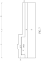
- FIG. 9 further illustrates a structural view of a semiconductor device according to an embodiment of the present invention.
- the semiconductor device preferably includes a HEMT region 14 and a capacitor region 16 defined on the substrate 12 , a mesa isolation 24 disposed on the HEMT region 14 , a HEMT 52 disposed on the mesa isolation 24 , a hard mask 28 surrounding the HEMT 52 and extending to the capacitor region 16 , a capacitor 54 disposed on the capacitor region 16 , and a buffer layer 18 disposed between the mesa isolation 24 , the capacitor 54 , and the substrate 12 , in which the mesa isolation 24 and the buffer layer 18 both include GaN.
- the HEMT 52 includes a barrier layer 20 disposed on the mesa isolation 24 , a p-type semiconductor layer 22 disposed on the barrier layer 20 , a gate electrode 44 disposed on the p-type semiconductor layer 22 , a source electrode 30 and drain electrode 32 adjacent to two sides of the gate electrode 44 , a source electrode extension 34 disposed on the source electrode 30 , and a drain electrode extension 36 disposed on the drain electrode 32 .
- the capacitor 54 on the other hand includes a bottom electrode 38 disposed on the hard mask 28 , a capacitor dielectric layer 42 disposed on the bottom electrode 38 while extending to the top surface and sidewall of the hard mask 28 on the HEMT region 14 , and a top electrode 46 disposed on the capacitor dielectric layer 42 .
- the thickness of the bottom electrode 38 in this embodiment is only equal to the overall thickness of the source electrode extension 34 or drain electrode extensions 36 on the HEMT region 14 .
- the overall thickness of the bottom electrode 38 is about 100 nm
- the thickness of the capacitor dielectric layer 42 is between 20-100 nm
- the thickness of the top electrode 46 is about 100 nm.
Landscapes
- Junction Field-Effect Transistors (AREA)
Abstract
A method for fabricating a semiconductor device includes the steps of providing a substrate having a high electron mobility transistor (HEMT) region and a capacitor region, forming a first mesa isolation on the HEMT region and a second mesa isolation on the capacitor region, forming a HEMT on the first mesa isolation, and then forming a capacitor on the second mesa isolation.
Description
This application is a continuation application of U.S. application Ser. No. 16/994,646, filed on Aug. 16, 2020. The content of the application is incorporated herein by reference.
The invention relates to a semiconductor device, and more particularly to a semiconductor device having integrated a high electron mobility transistor (HEMT) and a capacitor.
High electron mobility transistor (HEMT) fabricated from GaN-based materials have various advantages in electrical, mechanical, and chemical aspects of the field. For instance, advantages including wide band gap, high break down voltage, high electron mobility, high elastic modulus, high piezoelectric and piezoresistive coefficients, and chemical inertness. All of these advantages allow GaN-based materials to be used in numerous applications including high intensity light emitting diodes (LEDs), power switching devices, regulators, battery protectors, display panel drivers, and communication devices.
A semiconductor device includes a substrate having a high electron mobility transistor (HEMT) region and a capacitor region, a first mesa isolation on the HEMT region, a HEMT on the first mesa isolation, a second mesa isolation on the capacitor region, and a capacitor on the second mesa isolation. The semiconductor device further includes buffer layer between the substrate, the first mesa isolation, and the second mesa isolation, in which bottom surfaces of the first mesa isolation and the second mesa isolation are coplanar.
According to another aspect of the present invention, a semiconductor device includes a substrate having a high electron mobility transistor (HEMT) region and a capacitor region, a mesa isolation on the HEMT region, a HEMT on the mesa isolation, a capacitor on the capacitor region, and a buffer layer between the mesa isolation, the capacitor, and substrate.
According to yet another aspect of the present invention, a semiconductor device includes a substrate having a high electron mobility transistor (HEMT) region and a capacitor region, a mesa isolation on the HEMT region, a HEMT on the mesa isolation, a hard mask around the HEMT and extending to the capacitor region, and a capacitor on the hard mask.
These and other objectives of the present invention will no doubt become obvious to those of ordinary skill in the art after reading the following detailed description of the preferred embodiment that is illustrated in the various figures and drawings.
Referring to the FIGS. 1-3 , FIGS. 1-3 illustrate a method for fabricating a HEMT according to an embodiment of the present invention. As shown in the FIG. 1 , a substrate 12 such as a substrate made from silicon, silicon carbide, or aluminum oxide (or also referred to as sapphire) is provided, in which the substrate 12 could be a single-layered substrate, a multi-layered substrate, gradient substrate, or combination thereof. According to other embodiment of the present invention, the substrate 12 could also include a silicon-on-insulator (SOI) substrate. Next, a HEMT region 14 and a capacitor region 16 are defined on the substrate 12.
Next, a buffer layer 18 is formed on the surface of the substrate 12. According to an embodiment of the present invention, the buffer layer 18 is preferably made of III-V semiconductors such as gallium nitride (GaN), in which a thickness of the buffer layer 18 could be between 0.5 microns to 10 microns. According to an embodiment of the present invention, the formation of the buffer layer 18 could be accomplished by a molecular-beam epitaxy (MBE) process, a metal organic chemical vapor deposition (MOCVD) process, a chemical vapor deposition (CVD) process, a hydride vapor phase epitaxy (HVPE) process, or combination thereof.
Next, a barrier layer 20 is formed on the surface of the buffer layer 18. In this embodiment, the barrier layer 20 is preferably made of III-V semiconductor such as aluminum gallium nitride (AlxGa1-xN), in which 0<x<1, x being less than or equal to 20%, and the barrier layer 20 preferably includes an epitaxial layer formed through epitaxial growth process. Similar to the buffer layer 18, the formation of the barrier layer 20 on the buffer layer 18 could be accomplished by a molecular-beam epitaxy (MBE) process, a metal organic chemical vapor deposition (MOCVD) process, a chemical vapor deposition (CVD) process, a hydride vapor phase epitaxy (HVPE) process, or combination thereof. It should be noted that even though the barrier layer 20 is formed directly on the surface of the buffer layer 18, according to another embodiment of the present invention, it would also be desirable to form an extra metal nitride layer (not shown) including but not limited to for example aluminum nitride (AlN) between the buffer layer 18 and the barrier layer 20, which is also within the scope of the present invention.
Next, a p-type semiconductor layer 22 is formed on the barrier layer 20. In this embodiment, the p-type semiconductor layer 22 preferably is a III-V compound layer including p-type GaN (p-GaN) and the formation of the p-type semiconductor layer 22 on the surface of the barrier layer 20 could be accomplished by a molecular-beam epitaxy (MBE) process, a metal organic chemical vapor deposition (MOCVD) process, a chemical vapor deposition (CVD) process, a hydride vapor phase epitaxy (HVPE) process, or combination thereof.
Next, a MESA isolation process is conducted to form mesa isolations 24, 26 on the HEMT region 14 and capacitor region 16 respectively so that devices could be isolated to operate independently without affecting each other. In this embodiment, the MESA isolation process could be accomplished by conducting a photo-etching process to remove part of p-type semiconductor layer 22, part of the barrier layer 20, and part of the buffer layer 18, in which the patterned p-type semiconductor layer 22, the patterned barrier layer 20, and the patterned buffer layer 18 preferably share equal widths and edges of the three layers are aligned. The width of the remaining un-patterned buffer layer 18 is preferably equal to the width of the substrate 12. Preferably, each of the mesa isolations 24, 26 includes a patterned buffer layer 18, in which the thickness of the patterned buffer layer 18 is approximately 300 nm, the thickness of the patterned barrier layer 20 is approximately 10 nm, and the thickness of the patterned p-type semiconductor layer 22 is approximately 100 nm.
Next, as shown in FIG. 2 , a photo-etching process is conducted to remove part of the p-type semiconductor layer 22 on the HEMT region 14 and all of the p-type semiconductor layer 22 on the capacitor region 16 so that the remaining p-type semiconductor layer 22 is only disposed on the barrier layer 20 on HEMT region 14 while none of the p-type semiconductor layer 22 is remained on the surface of the barrier layer 20 on capacitor region 16, in which the patterned p-type semiconductor layer 22 preferably serves as part of the gate structure for the HEMT device in the later process. Next, a hard mask 28 is conformally formed on the buffer layer 18 to cover the mesa isolations 24, 26 on the HEMT region 14 and the capacitor region 16. In this embodiment, the hard mask 28 preferably includes silicon nitride and the thickness of the hard mask 28 is approximately 200 nm, but not limited thereto.
Next, one or more photo-etching process is conducted to remove part of the hard mask 28 and part of the barrier layer 20 on the HEMT region 14 for forming a plurality of recesses (not shown), a conductive material is formed into the recesses and on the surface of the hard mask 28 on both HEMT region 14 and capacitor region 16, and a pattern transfer process is conducted to remove part of the conductive material. Preferably, the conductive material deposited into the recesses on the HEMT region 14 serves as a source electrode 30 and drain electrode 32, the conductive material disposed on the source electrode 30 and drain electrode 32 and extended to the surface of the hard mask 28 adjacent to two sides of the source electrode 30 and drain electrode 32 serves as a source electrode extension 34 and drain electrode extension 36, and the conductive material being patterned on the surface of the hard mask 28 on the capacitor region 16 preferably serves as a bottom electrode 38 for the capacitor. Next, another hard mask 40 is formed on the surface of hard mask 28 on the HEMT region 14 and extending to the bottom electrode 38 on the capacitor region 16, in which the hard mask 40 on the capacitor region 16 preferably serves as a capacitor dielectric layer 42. In this embodiment, the thickness of the capacitor dielectric layer 42 is between 20-100 nm, but not limited thereto.
Next, as shown in FIG. 3 , one or more photo-etching process is conducted to remove part of the hard mask 40 and part of the hard mask 28 on the HEMT region 14 for forming a recess exposing the p-type semiconductor layer 22, another conductive material is formed on the hard mask 40 on HEMT region 14 to fill the recess completely while covering the surface of the hard mask 40 on the capacitor region 16, and a pattern transfer process is conducted to remove part of the conductive material, in which the conductive material deposited into the recess and part of the conductive material on the surface of the hard mask 40 on the HEMT region 14 preferably serves as a gate electrode 44 while the patterned conductive material layer on the capacitor region 16 serves as a top electrode for the capacitor.
In this embodiment, the gate electrode 44, source electrode 30, and drain electrode 32 are preferably made of metal, in which gate electrode 44 preferably includes Schottky metal while the source electrode 30 and the drain electrode 32 are preferably made of ohmic contact metals. According to an embodiment of the present invention, each of the gate electrode 44, source electrode 30, and drain electrode 32 could include gold (Au), silver (Ag), platinum (Pt), titanium (Ti), aluminum (Al), tungsten (W), palladium (Pd), or combination thereof. Moreover, it would be desirable to conduct an electroplating process, sputtering process, resistance heating evaporation process, electron beam evaporation process, physical vapor deposition (PVD) process, chemical vapor deposition (CVD) process, or combination thereof to form conductive materials in the aforementioned recesses and then pattern the conductive materials through single or multiple etching processes for forming the gate electrode 44, the source electrode 30, and the drain electrode 32.
Next, a contact plug formation could be conducted to form contact plugs 50 electrically connected to the gate electrode 44, source electrode 30, and drain electrode 32 on the HMET region 14 and the bottom electrode 38 and top electrode 46 on the capacitor region 16. In this embodiment, the formation of contact plugs 50 could be accomplished by first forming an interlayer dielectric (ILD) layer 48 on the hard mask 40 on both HEMT region 14 and capacitor region 16, removing part of the ILD layer 48 and part of the hard mask 40 to form contact holes (not shown), and then depositing a barrier layer (not shown) and a metal layer (not shown) into the contact holes. A planarizing process, such as chemical mechanical polishing (CMP) process is then conducted to remove part of the metal layer, part of the barrier layer, and even part of the ILD layer 48 to form contact plugs 50 in the contact holes, in which the top surface of the contact plugs 50 is even with the top surface of the ILD layer 48. In this embodiment, the barrier layer is selected from the group consisting of Ti, Ta, TiN, TaN, and WN and the metal layer is selected from the group consisting of Al, Ti, Ta, W, Nb, Mo, and Cu.
Referring again to FIG. 3 , FIG. 3 further illustrates a structural view of a semiconductor device according to an embodiment of the present invention. As shown in FIG. 3 , the semiconductor device preferably includes a HEMT region 14 and a capacitor region 16 defined on the substrate 12, a mesa isolation 24 disposed on the HEMT region 14, a HEMT 52 disposed on the mesa isolation 24, another mesa isolation 26 disposed on the capacitor region 16, a buffer layer 18 disposed on the substrate 12 and between the mesa isolations 24, 26, and a capacitor 54 disposed on the mesa isolation 26, in which the bottom surfaces of the mesa isolations 24, 26 are coplanar and both mesa isolations 24, 26 includes GaN.
The HEMT 52 includes a barrier layer 20 disposed on the mesa isolation 24, a p-type semiconductor layer 22 disposed on the barrier layer 20, a gate electrode 44 disposed on the p-type semiconductor layer 22, a source electrode 30 and drain electrode 32 adjacent to two sides of the gate electrode 44, a source electrode extension 34 disposed on the source electrode 30, a drain electrode extension 36 disposed on the drain electrode 32, and a hard mask 28 disposed on the mesa isolations 24, 26 and surrounding the source electrode 30 and drain electrode 32.
The capacitor 54 includes a bottom electrode 38 disposed on the hard mask 28, a capacitor dielectric layer 42 disposed on the bottom electrode 38 and extending to the top surface and sidewall of the hard mask 28 on the HEMT region 14, and a top electrode 46 disposed on the capacitor dielectric layer 42, in which the bottom surface of the bottom electrode 38 is even with the bottom surface of the source electrode extension 34 while the top surface of the top electrode 46 is even with the top surface of the gate electrode 44.
Referring to FIGS. 4-6 , FIGS. 4-6 illustrate a method for fabricating a HEMT according to an embodiment of the present invention. For simplicity purpose, elements from the aforementioned embodiments are labeled with same numberings. As shown in the FIG. 4 , a substrate 12 such as a substrate made from silicon, silicon carbide, or aluminum oxide (or also referred to as sapphire) is provided, in which the substrate 12 could be a single-layered substrate, a multi-layered substrate, gradient substrate, or combination thereof. According to other embodiment of the present invention, the substrate 12 could also include a silicon-on-insulator (SOI) substrate. Next, a HEMT region 14 and a capacitor region 16 are defined on the substrate 12.
Next, a buffer layer 18 is formed on the surface of the substrate 12. According to an embodiment of the present invention, the buffer layer 18 is preferably made of III-V semiconductors such as gallium nitride (GaN), in which a thickness of the buffer layer 18 could be between 0.5 microns to 10 microns. According to an embodiment of the present invention, the formation of the buffer layer 18 could be accomplished by a molecular-beam epitaxy (MBE) process, a metal organic chemical vapor deposition (MOCVD) process, a chemical vapor deposition (CVD) process, a hydride vapor phase epitaxy (HVPE) process, or combination thereof.
Next, a barrier layer 20 is formed on the surface of the buffer layer 18. In this embodiment, the barrier layer 20 is preferably made of III-V semiconductor such as aluminum gallium nitride (AlxGa1-xN), in which 0<x<1, x being less than or equal to 20%, and the barrier layer 20 preferably includes an epitaxial layer formed through epitaxial growth process. Similar to the buffer layer 18, the formation of the barrier layer 20 on the buffer layer 18 could be accomplished by a molecular-beam epitaxy (MBE) process, a metal organic chemical vapor deposition (MOCVD) process, a chemical vapor deposition (CVD) process, a hydride vapor phase epitaxy (HVPE) process, or combination thereof. It should be noted that even though the barrier layer 20 is formed directly on the surface of the buffer layer 18, according to another embodiment of the present invention, it would also be desirable to form an extra metal nitride layer (not shown) including but not limited to for example aluminum nitride (AlN) between the buffer layer 18 and the barrier layer 20, which is also within the scope of the present invention.
Next, a p-type semiconductor layer 22 is formed on the barrier layer 20. In this embodiment, the p-type semiconductor layer 22 preferably is a III-V compound layer including p-type GaN (p-GaN) and the formation of the p-type semiconductor layer 22 on the surface of the barrier layer 20 could be accomplished by a molecular-beam epitaxy (MBE) process, a metal organic chemical vapor deposition (MOCVD) process, a chemical vapor deposition (CVD) process, a hydride vapor phase epitaxy (HVPE) process, or combination thereof.
Next, a MESA isolation process is conducted to form a mesa isolation 24 on the HEMT region 14. In this embodiment, the MESA isolation process could be accomplished by conducting a photo-etching process to remove part of p-type semiconductor layer 22, part of the barrier layer 20, and part of the buffer layer 18, in which the patterned p-type semiconductor layer 22, the patterned barrier layer 20, and the patterned buffer layer 18 preferably share equal widths and edges of the three layers are aligned. The width of the remaining un-patterned buffer layer 18 is preferably equal to the width of the substrate 12. Preferably, the mesa isolation 24 includes a patterned buffer layer 18, in which the thickness of the patterned buffer layer 18 is approximately 300 nm, the thickness of the patterned barrier layer 20 is approximately 10 nm, and the thickness of the patterned p-type semiconductor layer 22 is approximately 100 nm.
Next, as shown in FIG. 5 , a photo-etching process is conducted to remove part of the p-type semiconductor layer 22 on the HEMT region 14, in which the patterned p-type semiconductor layer 22 preferably serves as part of the gate structure for the HEMT device in the later process. Next, a hard mask 28 is conformally formed on the buffer layer 18 to cover the mesa isolation 24 on the HEMT region 14 while extending to the buffer layer 18 on the capacitor region 16. In this embodiment, the hard mask 28 preferably includes silicon nitride and the thickness of the hard mask 28 is approximately 200 nm, but not limited thereto.
Next, one or more photo-etching process is conducted to remove part of the hard mask 28 and part of the barrier layer 20 on the HEMT region 14 and majority of the hard mask 28 on the capacitor region 16 for forming a plurality of recesses (not shown), a conductive material is formed into the recesses on both HEMT region 14 and capacitor region 16, and a pattern transfer process is conducted to remove part of the conductive material. Preferably, the conductive material deposited into the recesses on the HEMT region 14 serves as a source electrode 30 and drain electrode 32, the conductive material disposed on the source electrode 30 and drain electrode 32 and extended to the surface of the hard mask 28 adjacent to two sides of the source electrode 30 and drain electrode 32 serves as a source electrode extension 34 and drain electrode extension 36, and the conductive material being formed into the recess or trench on the capacitor region 16 preferably serves as a bottom electrode 38 for the capacitor. Next, another hard mask 40 is formed on the surface of hard mask 28 on the HEMT region 14 and extending to the bottom electrode 38 on the capacitor region 16, in which the hard mask 40 on the capacitor region 16 preferably serves as a capacitor dielectric layer 42. In this embodiment, the thickness of the capacitor dielectric layer 42 is between 20-100 nm, but not limited thereto.
Next, as shown in FIG. 6 , one or more photo-etching process is conducted to remove part of the hard mask 40 and part of the hard mask 28 on the HEMT region 14 for forming a recess exposing the p-type semiconductor layer 22, another conductive material is formed on the hard mask 40 on HEMT region 14 to fill the recess completely while covering the surface of the hard mask 40 on the capacitor region 16, and a pattern transfer process is conducted to remove part of the conductive material, in which the conductive material deposited into the recess and part of the conductive material on the surface of the hard mask 40 on the HEMT region 14 preferably serves as a T-shape gate electrode 44 while the patterned conductive material layer on the capacitor region 16 serves as a top electrode 46 for the capacitor.
Similar to the aforementioned embodiment, the gate electrode 44, source electrode 30, and drain electrode 32 are preferably made of metal, in which gate electrode 44 preferably includes Schottky metal while the source electrode 30 and the drain electrode 32 are preferably made of ohmic contact metals. According to an embodiment of the present invention, each of the gate electrode 44, source electrode 30, and drain electrode 32 could include gold (Au), silver (Ag), platinum (Pt), titanium (Ti), aluminum (Al), tungsten (W), palladium (Pd), or combination thereof. Moreover, it would be desirable to conduct an electroplating process, sputtering process, resistance heating evaporation process, electron beam evaporation process, physical vapor deposition (PVD) process, chemical vapor deposition (CVD) process, or combination thereof to form conductive materials in the aforementioned recesses and then pattern the conductive materials through single or multiple etching processes for forming the gate electrode 44, the source electrode 30, and the drain electrode 32.
Next, a contact plug formation could be conducted to form contact plugs 50 electrically connected to the gate electrode 44, source electrode 30, and drain electrode 32 on the HMET region 14 and the bottom electrode 38 and top electrode 46 on the capacitor region 16. In this embodiment, the formation of contact plugs 50 could be accomplished by first forming an interlayer dielectric (ILD) layer 48 on the hard mask 40 on both HEMT region 14 and capacitor region 16, removing part of the ILD layer 48 and part of the hard mask 40 to form contact holes (not shown), and then depositing a barrier layer (not shown) and a metal layer (not shown) into the contact holes. A planarizing process, such as chemical mechanical polishing (CMP) process is then conducted to remove part of the metal layer, part of the barrier layer, and even part of the ILD layer 48 to form contact plugs 50 in the contact holes, in which the top surface of the contact plugs 50 is even with the top surface of the ILD layer 48. In this embodiment, the barrier layer is selected from the group consisting of Ti, Ta, TiN, TaN, and WN and the metal layer is selected from the group consisting of Al, Ti, Ta, W, Nb, Mo, and Cu.
Referring again to FIG. 6 , FIG. 6 further illustrates a structural view of a semiconductor device according to an embodiment of the present invention. As shown in FIG. 6 , the semiconductor device preferably includes a HEMT region 14 and a capacitor region 16 defined on the substrate 12, a mesa isolation 24 disposed on the HEMT region 14, a HEMT 52 disposed on the mesa isolation 24, a capacitor 54 disposed on the capacitor region 16, and a buffer layer 18 disposed between the mesa isolation 24, the capacitor 54, and the substrate 12, in which the mesa isolation 24 and the buffer layer 18 both include GaN.
The HEMT 52 includes a barrier layer 20 disposed on the mesa isolation 24, a p-type semiconductor layer 22 disposed on the barrier layer 20, a gate electrode 44 disposed on the p-type semiconductor layer 22, a source electrode 30 and drain electrode 32 adjacent to two sides of the gate electrode 44, a source electrode extension 34 disposed on the source electrode 30, a drain electrode extension 36 disposed on the drain electrode 32, and a hard mask 28 disposed on the mesa isolation 24 and surrounding the source electrode 30 and drain electrode 32.
The capacitor 54 on the other hand includes a bottom electrode 38 disposed on the hard mask 28, a capacitor dielectric layer 42 disposed on the bottom electrode 38 while extending to the top surface and sidewall of the hard mask 28 on the HEMT region 14, and a top electrode 46 disposed on the capacitor dielectric layer 42. In contrast to the aforementioned embodiment having mesa isolations 24, 26 on both HEMT region 14 and capacitor region 16, only a mesa isolation 24 is disposed on the HEMT region 14 in this embodiment while the capacitor region 16 includes no mesa isolation so that the bottom electrode 38 would contact the top surface of the buffer layer 18 directly while having a T-shape cross-section. Moreover, the overall thickness of the bottom electrode 38 is substantially equal to the combined thickness of the source electrode 30 and source electrode extension 34 or the combined thickness of the drain electrode 32 and drain electrode extension 36 on the HEMT region 14. Preferably, the overall thickness of the bottom electrode 38 is about 300 nm, the thickness of the capacitor dielectric layer 42 is between 20-100 nm, and the thickness of the top electrode 46 is about 100 nm.
Referring to FIGS. 7-9 , FIGS. 7-9 illustrate a method for fabricating a HEMT according to an embodiment of the present invention. For simplicity purpose, elements from the aforementioned embodiments are labeled with same numberings. As shown in the FIG. 7 , a substrate 12 such as a substrate made from silicon, silicon carbide, or aluminum oxide (or also referred to as sapphire) is provided, in which the substrate 12 could be a single-layered substrate, a multi-layered substrate, gradient substrate, or combination thereof. According to other embodiment of the present invention, the substrate 12 could also include a silicon-on-insulator (SOI) substrate. Next, a HEMT region 14 and a capacitor region 16 are defined on the substrate 12.
Next, a buffer layer 18 is formed on the surface of the substrate 12. According to an embodiment of the present invention, the buffer layer 18 is preferably made of III-V semiconductors such as gallium nitride (GaN), in which a thickness of the buffer layer 18 could be between 0.5 microns to 10 microns. According to an embodiment of the present invention, the formation of the buffer layer 18 could be accomplished by a molecular-beam epitaxy (MBE) process, a metal organic chemical vapor deposition (MOCVD) process, a chemical vapor deposition (CVD) process, a hydride vapor phase epitaxy (HVPE) process, or combination thereof.
Next, a barrier layer 20 is formed on the surface of the buffer layer 18. In this embodiment, the barrier layer 20 is preferably made of III-V semiconductor such as aluminum gallium nitride (AlxGa1-xN), in which 0<x<1, x being less than or equal to 20%, and the barrier layer 20 preferably includes an epitaxial layer formed through epitaxial growth process. Similar to the buffer layer 18, the formation of the barrier layer 20 on the buffer layer 18 could be accomplished by a molecular-beam epitaxy (MBE) process, a metal organic chemical vapor deposition (MOCVD) process, a chemical vapor deposition (CVD) process, a hydride vapor phase epitaxy (HVPE) process, or combination thereof. It should be noted that even though the barrier layer 20 is formed directly on the surface of the buffer layer 18, according to another embodiment of the present invention, it would also be desirable to form an extra metal nitride layer (not shown) including but not limited to for example aluminum nitride (AlN) between the buffer layer 18 and the barrier layer 20, which is also within the scope of the present invention.
Next, a p-type semiconductor layer 22 is formed on the barrier layer 20. In this embodiment, the p-type semiconductor layer 22 preferably is a III-V compound layer including p-type GaN (p-GaN) and the formation of the p-type semiconductor layer 22 on the surface of the barrier layer 20 could be accomplished by a molecular-beam epitaxy (MBE) process, a metal organic chemical vapor deposition (MOCVD) process, a chemical vapor deposition (CVD) process, a hydride vapor phase epitaxy (HVPE) process, or combination thereof.
Next, a MESA isolation process is conducted to form a mesa isolation 24 on the HEMT region 14. In this embodiment, the MESA isolation process could be accomplished by conducting a photo-etching process to remove part of p-type semiconductor layer 22, part of the barrier layer 20, and part of the buffer layer 18, in which the patterned p-type semiconductor layer 22, the patterned barrier layer 20, and the patterned buffer layer 18 preferably share equal widths and edges of the three layers are aligned. The width of the remaining un-patterned buffer layer 18 is preferably equal to the width of the substrate 12. Preferably, the mesa isolation 24 includes a patterned buffer layer 18, in which the thickness of the patterned buffer layer 18 is approximately 300 nm, the thickness of the patterned barrier layer 20 is approximately 10 nm, and the thickness of the patterned p-type semiconductor layer 22 is approximately 100 nm.
Next, a photo-etching process is conducted to remove part of the p-type semiconductor layer 22 on the HEMT region 14, in which the patterned p-type semiconductor layer 22 preferably serves as part of the gate structure for the HEMT device in the later process. Next, a hard mask 28 is conformally formed on the buffer layer 18 to cover the mesa isolation 24 on the HEMT region 14 while extending to the buffer layer 18 on the capacitor region 16. In this embodiment, the hard mask 28 preferably includes silicon nitride and the thickness of the hard mask 28 is approximately 200 nm, but not limited thereto.
Next, as shown in FIG. 8 , one or more photo-etching process is conducted to remove part of the hard mask 28 and part of the barrier layer 20 on the HEMT region 14 for forming a plurality of recesses (not shown), a conductive material is formed into the recesses on the HEMT region 14 and onto the surface of the hard mask 28 on the capacitor region 16, and a pattern transfer process is conducted to remove part of the conductive material. Preferably, the conductive material deposited into the recesses on the HEMT region 14 serves as a source electrode 30 and drain electrode 32, the conductive material disposed on the source electrode 30 and drain electrode 32 and extended to the surface of the hard mask 28 adjacent to two sides of the source electrode 30 and drain electrode 32 serves as a source electrode extension 34 and drain electrode extension 36, and the conductive material formed on the surface of the hard mask 28 on the capacitor region 16 preferably serves as a bottom electrode 38 for the capacitor. Next, another hard mask 40 is formed on the surface of hard mask 28 on the HEMT region 14 and extending to the bottom electrode 38 on the capacitor region 16, in which the hard mask 40 on the capacitor region 16 preferably serves as a capacitor dielectric layer 42. In this embodiment, the thickness of the capacitor dielectric layer 42 is between 20-100 nm, but not limited thereto.
Next, as shown in FIG. 9 , one or more photo-etching process is conducted to remove part of the hard mask 40 and part of the hard mask 28 on the HEMT region 14 for forming a recess exposing the p-type semiconductor layer 22, another conductive material is formed on the hard mask 40 on HEMT region 14 to fill the recess completely while covering the surface of the hard mask 40 on the capacitor region 16, and a pattern transfer process is conducted to remove part of the conductive material, in which the conductive material deposited into the recess and part of the conductive material on the surface of the hard mask 40 on the HEMT region 14 preferably serves as a T-shape gate electrode 44 while the patterned conductive material layer on the capacitor region 16 serves as a top electrode 46 for the capacitor.
Similar to the aforementioned embodiment, the gate electrode 44, source electrode 30, and drain electrode 32 are preferably made of metal, in which gate electrode 44 preferably includes Schottky metal while the source electrode 30 and the drain electrode 32 are preferably made of ohmic contact metals. According to an embodiment of the present invention, each of the gate electrode 44, source electrode 30, and drain electrode 32 could include gold (Au), silver (Ag), platinum (Pt), titanium (Ti), aluminum (Al), tungsten (W), palladium (Pd), or combination thereof. Moreover, it would be desirable to conduct an electroplating process, sputtering process, resistance heating evaporation process, electron beam evaporation process, physical vapor deposition (PVD) process, chemical vapor deposition (CVD) process, or combination thereof to form conductive materials in the aforementioned recesses and then pattern the conductive materials through single or multiple etching processes for forming the gate electrode 44, the source electrode 30, and the drain electrode 32.
Next, a contact plug formation could be conducted to form contact plugs 50 electrically connected to the gate electrode 44, source electrode 30, and drain electrode 32 on the HMET region 14 and the bottom electrode 38 and top electrode 46 on the capacitor region 16. In this embodiment, the formation of contact plugs 50 could be accomplished by first forming an interlayer dielectric (ILD) layer 48 on the hard mask 40 on both HEMT region 14 and capacitor region 16, removing part of the ILD layer 48 and part of the hard mask 40 to form contact holes (not shown), and then depositing a barrier layer (not shown) and a metal layer (not shown) into the contact holes. A planarizing process, such as chemical mechanical polishing (CMP) process is then conducted to remove part of the metal layer, part of the barrier layer, and even part of the ILD layer 48 to form contact plugs 50 in the contact holes, in which the top surface of the contact plugs 50 is even with the top surface of the ILD layer 48. In this embodiment, the barrier layer is selected from the group consisting of Ti, Ta, TiN, TaN, and WN and the metal layer is selected from the group consisting of Al, Ti, Ta, W, Nb, Mo, and Cu.
Referring again to FIG. 9 , FIG. 9 further illustrates a structural view of a semiconductor device according to an embodiment of the present invention. As shown in FIG. 9 , the semiconductor device preferably includes a HEMT region 14 and a capacitor region 16 defined on the substrate 12, a mesa isolation 24 disposed on the HEMT region 14, a HEMT 52 disposed on the mesa isolation 24, a hard mask 28 surrounding the HEMT 52 and extending to the capacitor region 16, a capacitor 54 disposed on the capacitor region 16, and a buffer layer 18 disposed between the mesa isolation 24, the capacitor 54, and the substrate 12, in which the mesa isolation 24 and the buffer layer 18 both include GaN.
The HEMT 52 includes a barrier layer 20 disposed on the mesa isolation 24, a p-type semiconductor layer 22 disposed on the barrier layer 20, a gate electrode 44 disposed on the p-type semiconductor layer 22, a source electrode 30 and drain electrode 32 adjacent to two sides of the gate electrode 44, a source electrode extension 34 disposed on the source electrode 30, and a drain electrode extension 36 disposed on the drain electrode 32.
The capacitor 54 on the other hand includes a bottom electrode 38 disposed on the hard mask 28, a capacitor dielectric layer 42 disposed on the bottom electrode 38 while extending to the top surface and sidewall of the hard mask 28 on the HEMT region 14, and a top electrode 46 disposed on the capacitor dielectric layer 42. In contrast to the bottom electrode 38 disposed directly on the buffer layer 18 while the overall thickness of the bottom electrode 38 is equivalent to the combined thickness of the source electrode 30 and source electrode extension 34 or the combined thickness of drain electrode 32 and drain electrode extension 36 on HEMT region 14 in the aforementioned embodiment, the thickness of the bottom electrode 38 in this embodiment is only equal to the overall thickness of the source electrode extension 34 or drain electrode extensions 36 on the HEMT region 14. Preferably, the overall thickness of the bottom electrode 38 is about 100 nm, the thickness of the capacitor dielectric layer 42 is between 20-100 nm, and the thickness of the top electrode 46 is about 100 nm.
Those skilled in the art will readily observe that numerous modifications and alterations of the device and method may be made while retaining the teachings of the invention. Accordingly, the above disclosure should be construed as limited only by the metes and bounds of the appended claims.
Claims (10)
1. A method for fabricating a semiconductor device, comprising:
providing a substrate having a high electron mobility transistor (HEMT) region and a capacitor region;
forming a first mesa isolation on the HEMT region and a second mesa isolation on the capacitor region;
forming a HEMT on the first mesa isolation; and
forming a capacitor on the second mesa isolation.
2. The method of claim 1 , further comprising:
forming a barrier layer on the substrate;
forming a p-type semiconductor layer on the barrier layer;
patterning the p-type semiconductor layer, the barrier layer, and the substrate to form the first mesa isolation and the second mesa isolation;
removing the p-type semiconductor layer on the capacitor region;
forming a first hard mask on the first mesa isolation and the second mesa isolation;
forming a source electrode and a drain electrode in the first hard mask on the HEMT region;
forming a source electrode extension and a drain electrode extension on the HEMT region;
forming a bottom electrode on the first hard mask of the capacitor region;
forming a second hard mask on the source electrode extension, the drain electrode extension, and the bottom electrode; and
forming a gate electrode on the HEMT region and a top electrode on the capacitor region.
3. The method of claim 2 , further comprising patterning the p-type semiconductor layer on the HEMT region and removing the p-type semiconductor layer on the capacitor region at the same time.
4. The method of claim 2 , further comprising forming the source electrode extension and the bottom electrode at the same time.
5. The method of claim 2 , wherein bottom surfaces of the source electrode extension and the bottom electrode are coplanar.
6. The method of claim 2 , further comprising:
removing the second hard mask and the first hard mask to form a recess exposing the p-type semiconductor layer; and
forming the gate electrode in the recess and the top electrode on the capacitor region.
7. The method of claim 2 , wherein top surfaces of the gate electrode and the top electrode are coplanar.
8. The method of claim 2 , wherein bottom surfaces of the gate electrode and the top electrode are coplanar.
9. The method of claim 1 , wherein bottom surfaces of the first mesa isolation and the second mesa isolation are coplanar.
10. The method of claim 1 , wherein the first mesa isolation and the second mesa comprise gallium nitride (GaN).
Priority Applications (3)
| Application Number | Priority Date | Filing Date | Title |
|---|---|---|---|
| US18/144,822 US11973133B2 (en) | 2020-07-21 | 2023-05-08 | High electron mobility transistor and method for fabricating the same |
| US18/614,735 US12206018B2 (en) | 2020-07-21 | 2024-03-24 | High electron mobility transistor and method for fabricating the same |
| US18/979,667 US20250113523A1 (en) | 2020-07-21 | 2024-12-13 | High electron mobility transistor and method for fabricating the same |
Applications Claiming Priority (4)
| Application Number | Priority Date | Filing Date | Title |
|---|---|---|---|
| CN202010704978.1 | 2020-07-21 | ||
| CN202010704978.1A CN113964119A (en) | 2020-07-21 | 2020-07-21 | semiconductor element |
| US16/994,646 US11688800B2 (en) | 2020-07-21 | 2020-08-16 | High electron mobility transistor and method for fabricating the same |
| US18/144,822 US11973133B2 (en) | 2020-07-21 | 2023-05-08 | High electron mobility transistor and method for fabricating the same |
Related Parent Applications (1)
| Application Number | Title | Priority Date | Filing Date |
|---|---|---|---|
| US16/994,646 Continuation US11688800B2 (en) | 2020-07-21 | 2020-08-16 | High electron mobility transistor and method for fabricating the same |
Related Child Applications (1)
| Application Number | Title | Priority Date | Filing Date |
|---|---|---|---|
| US18/614,735 Continuation US12206018B2 (en) | 2020-07-21 | 2024-03-24 | High electron mobility transistor and method for fabricating the same |
Publications (2)
| Publication Number | Publication Date |
|---|---|
| US20230275147A1 US20230275147A1 (en) | 2023-08-31 |
| US11973133B2 true US11973133B2 (en) | 2024-04-30 |
Family
ID=79459966
Family Applications (7)
| Application Number | Title | Priority Date | Filing Date |
|---|---|---|---|
| US16/994,646 Active 2041-01-30 US11688800B2 (en) | 2020-07-21 | 2020-08-16 | High electron mobility transistor and method for fabricating the same |
| US18/144,822 Active US11973133B2 (en) | 2020-07-21 | 2023-05-08 | High electron mobility transistor and method for fabricating the same |
| US18/144,811 Active US12009415B2 (en) | 2020-07-21 | 2023-05-08 | High electron mobility transistor and method for fabricating the same |
| US18/614,735 Active US12206018B2 (en) | 2020-07-21 | 2024-03-24 | High electron mobility transistor and method for fabricating the same |
| US18/656,574 Active US12396194B2 (en) | 2020-07-21 | 2024-05-06 | High electron mobility transistor and method for fabricating the same |
| US18/979,667 Pending US20250113523A1 (en) | 2020-07-21 | 2024-12-13 | High electron mobility transistor and method for fabricating the same |
| US19/267,624 Pending US20250344430A1 (en) | 2020-07-21 | 2025-07-13 | High electron mobility transistor and method for fabricating the same |
Family Applications Before (1)
| Application Number | Title | Priority Date | Filing Date |
|---|---|---|---|
| US16/994,646 Active 2041-01-30 US11688800B2 (en) | 2020-07-21 | 2020-08-16 | High electron mobility transistor and method for fabricating the same |
Family Applications After (5)
| Application Number | Title | Priority Date | Filing Date |
|---|---|---|---|
| US18/144,811 Active US12009415B2 (en) | 2020-07-21 | 2023-05-08 | High electron mobility transistor and method for fabricating the same |
| US18/614,735 Active US12206018B2 (en) | 2020-07-21 | 2024-03-24 | High electron mobility transistor and method for fabricating the same |
| US18/656,574 Active US12396194B2 (en) | 2020-07-21 | 2024-05-06 | High electron mobility transistor and method for fabricating the same |
| US18/979,667 Pending US20250113523A1 (en) | 2020-07-21 | 2024-12-13 | High electron mobility transistor and method for fabricating the same |
| US19/267,624 Pending US20250344430A1 (en) | 2020-07-21 | 2025-07-13 | High electron mobility transistor and method for fabricating the same |
Country Status (2)
| Country | Link |
|---|---|
| US (7) | US11688800B2 (en) |
| CN (1) | CN113964119A (en) |
Families Citing this family (2)
| Publication number | Priority date | Publication date | Assignee | Title |
|---|---|---|---|---|
| CN116960150A (en) * | 2022-04-19 | 2023-10-27 | 联华电子股份有限公司 | high electron mobility transistor |
| CN115440674B (en) * | 2022-09-23 | 2023-11-17 | 上海新微半导体有限公司 | HEMT device and capacitor integrated structure, integration method thereof and power amplifier |
Citations (18)
| Publication number | Priority date | Publication date | Assignee | Title |
|---|---|---|---|---|
| US20060197134A1 (en) | 2005-03-03 | 2006-09-07 | Texas Instruments, Inc. | Method of manufacturing a metal-insulator-metal capacitor using an etchback process |
| US20070170548A1 (en) | 2006-01-25 | 2007-07-26 | Susumu Akamatsu | Semiconductor device and method for fabricating the same |
| US20070267705A1 (en) | 2006-05-22 | 2007-11-22 | Samsung Electronics Co., Ltd. | Semiconductor integrated circuit device having MIM capacitor and method of fabricating the same |
| US20130020570A1 (en) | 2011-07-22 | 2013-01-24 | Semiconductor Energy Laboratory Co., Ltd. | Semiconductor device |
| US20130026541A1 (en) | 2011-07-25 | 2013-01-31 | Renesas Electronics Corporation | Semiconductor integrated circuit device |
| US20130178021A1 (en) | 2012-01-06 | 2013-07-11 | International Business Machines Corporation | Integrated circuit with a thin body field effect transistor and capacitor |
| US20130200365A1 (en) | 2012-02-02 | 2013-08-08 | Semiconductor Energy Laboratory Co., Ltd. | Semiconductor device |
| US20130203214A1 (en) | 2012-02-07 | 2013-08-08 | Semiconductor Energy Laboratory Co., Ltd. | Method for manufacturing semiconductor device |
| US20130277680A1 (en) | 2012-04-23 | 2013-10-24 | Bruce M. Green | High Speed Gallium Nitride Transistor Devices |
| CN104158503A (en) | 2014-08-20 | 2014-11-19 | 无锡研奥电子科技有限公司 | X-waveband power amplifier based on GaN |
| US20150137135A1 (en) * | 2013-11-19 | 2015-05-21 | Bruce M. Green | Semiconductor devices with integrated schotky diodes and methods of fabrication |
| US20150348997A1 (en) | 2014-05-30 | 2015-12-03 | Semiconductor Energy Laboratory Co., Ltd. | Semiconductor device and method for manufacturing the same |
| US20160247832A1 (en) | 2015-02-20 | 2016-08-25 | Semiconductor Energy Laboratory Co., Ltd. | Semiconductor device and method for manufacturing the same |
| US20170018617A1 (en) | 2015-07-17 | 2017-01-19 | Cambridge Electronics, Inc. | Field-plate structures for semiconductor devices |
| US20170025406A1 (en) | 2015-07-21 | 2017-01-26 | Delta Electronics, Inc. | Semiconductor device |
| US20170170233A1 (en) | 2014-12-30 | 2017-06-15 | Win Semiconductors Corp. | Integrated structures of acoustic wave device and varactor, and acoustic wave device, varactor and power amplifier, and fabrication methods thereof |
| US20200373302A1 (en) | 2017-12-06 | 2020-11-26 | Semiconductor Energy Laboratory Co., Ltd. | Semiconductor device |
| US11276764B1 (en) | 2020-08-09 | 2022-03-15 | Global Communication Semiconductors, Llc | Method of making high frequency InGaP/GaAs HBTs |
Family Cites Families (10)
| Publication number | Priority date | Publication date | Assignee | Title |
|---|---|---|---|---|
| US7687327B2 (en) * | 2005-07-08 | 2010-03-30 | Kovio, Inc, | Methods for manufacturing RFID tags and structures formed therefrom |
| US20070278523A1 (en) * | 2006-06-05 | 2007-12-06 | Win Semiconductors Corp. | Structure and a method for monolithic integration of HBT, depletion-mode HEMT and enhancement-mode HEMT on the same substrate |
| JP2013041986A (en) * | 2011-08-16 | 2013-02-28 | Advanced Power Device Research Association | GaN-BASED SEMICONDUCTOR DEVICE |
| US9331076B2 (en) * | 2014-05-02 | 2016-05-03 | International Business Machines Corporation | Group III nitride integration with CMOS technology |
| US10679860B2 (en) * | 2015-03-09 | 2020-06-09 | Agency For Science, Technology And Research | Self-aligning source, drain and gate process for III-V nitride MISHEMTs |
| JP2018056506A (en) * | 2016-09-30 | 2018-04-05 | ルネサスエレクトロニクス株式会社 | Semiconductor device |
| US10263013B2 (en) * | 2017-02-24 | 2019-04-16 | Globalfoundries Inc. | Method of forming an integrated circuit (IC) with hallow trench isolation (STI) regions and the resulting IC structure |
| US10153273B1 (en) * | 2017-12-05 | 2018-12-11 | Northrop Grumman Systems Corporation | Metal-semiconductor heterodimension field effect transistors (MESHFET) and high electron mobility transistor (HEMT) based device and method of making the same |
| US10644142B2 (en) * | 2017-12-22 | 2020-05-05 | Nxp Usa, Inc. | Semiconductor devices with doped regions functioning as enhanced resistivity regions or diffusion barriers, and methods of fabrication therefor |
| WO2020191357A1 (en) * | 2019-03-21 | 2020-09-24 | Transphorm Technology, Inc. | Integrated design for iii-nitride devices |
-
2020
- 2020-07-21 CN CN202010704978.1A patent/CN113964119A/en active Pending
- 2020-08-16 US US16/994,646 patent/US11688800B2/en active Active
-
2023
- 2023-05-08 US US18/144,822 patent/US11973133B2/en active Active
- 2023-05-08 US US18/144,811 patent/US12009415B2/en active Active
-
2024
- 2024-03-24 US US18/614,735 patent/US12206018B2/en active Active
- 2024-05-06 US US18/656,574 patent/US12396194B2/en active Active
- 2024-12-13 US US18/979,667 patent/US20250113523A1/en active Pending
-
2025
- 2025-07-13 US US19/267,624 patent/US20250344430A1/en active Pending
Patent Citations (18)
| Publication number | Priority date | Publication date | Assignee | Title |
|---|---|---|---|---|
| US20060197134A1 (en) | 2005-03-03 | 2006-09-07 | Texas Instruments, Inc. | Method of manufacturing a metal-insulator-metal capacitor using an etchback process |
| US20070170548A1 (en) | 2006-01-25 | 2007-07-26 | Susumu Akamatsu | Semiconductor device and method for fabricating the same |
| US20070267705A1 (en) | 2006-05-22 | 2007-11-22 | Samsung Electronics Co., Ltd. | Semiconductor integrated circuit device having MIM capacitor and method of fabricating the same |
| US20130020570A1 (en) | 2011-07-22 | 2013-01-24 | Semiconductor Energy Laboratory Co., Ltd. | Semiconductor device |
| US20130026541A1 (en) | 2011-07-25 | 2013-01-31 | Renesas Electronics Corporation | Semiconductor integrated circuit device |
| US20130178021A1 (en) | 2012-01-06 | 2013-07-11 | International Business Machines Corporation | Integrated circuit with a thin body field effect transistor and capacitor |
| US20130200365A1 (en) | 2012-02-02 | 2013-08-08 | Semiconductor Energy Laboratory Co., Ltd. | Semiconductor device |
| US20130203214A1 (en) | 2012-02-07 | 2013-08-08 | Semiconductor Energy Laboratory Co., Ltd. | Method for manufacturing semiconductor device |
| US20130277680A1 (en) | 2012-04-23 | 2013-10-24 | Bruce M. Green | High Speed Gallium Nitride Transistor Devices |
| US20150137135A1 (en) * | 2013-11-19 | 2015-05-21 | Bruce M. Green | Semiconductor devices with integrated schotky diodes and methods of fabrication |
| US20150348997A1 (en) | 2014-05-30 | 2015-12-03 | Semiconductor Energy Laboratory Co., Ltd. | Semiconductor device and method for manufacturing the same |
| CN104158503A (en) | 2014-08-20 | 2014-11-19 | 无锡研奥电子科技有限公司 | X-waveband power amplifier based on GaN |
| US20170170233A1 (en) | 2014-12-30 | 2017-06-15 | Win Semiconductors Corp. | Integrated structures of acoustic wave device and varactor, and acoustic wave device, varactor and power amplifier, and fabrication methods thereof |
| US20160247832A1 (en) | 2015-02-20 | 2016-08-25 | Semiconductor Energy Laboratory Co., Ltd. | Semiconductor device and method for manufacturing the same |
| US20170018617A1 (en) | 2015-07-17 | 2017-01-19 | Cambridge Electronics, Inc. | Field-plate structures for semiconductor devices |
| US20170025406A1 (en) | 2015-07-21 | 2017-01-26 | Delta Electronics, Inc. | Semiconductor device |
| US20200373302A1 (en) | 2017-12-06 | 2020-11-26 | Semiconductor Energy Laboratory Co., Ltd. | Semiconductor device |
| US11276764B1 (en) | 2020-08-09 | 2022-03-15 | Global Communication Semiconductors, Llc | Method of making high frequency InGaP/GaAs HBTs |
Also Published As
| Publication number | Publication date |
|---|---|
| US20250113523A1 (en) | 2025-04-03 |
| US12396194B2 (en) | 2025-08-19 |
| US20240290875A1 (en) | 2024-08-29 |
| US12009415B2 (en) | 2024-06-11 |
| US20220029005A1 (en) | 2022-01-27 |
| US20230275146A1 (en) | 2023-08-31 |
| US11688800B2 (en) | 2023-06-27 |
| CN113964119A (en) | 2022-01-21 |
| US20240234559A1 (en) | 2024-07-11 |
| US20250344430A1 (en) | 2025-11-06 |
| US12206018B2 (en) | 2025-01-21 |
| US20230275147A1 (en) | 2023-08-31 |
Similar Documents
| Publication | Publication Date | Title |
|---|---|---|
| US20210013334A1 (en) | High electron mobility transistor and method for fabricating the same | |
| US20230369448A1 (en) | High electron mobility transistor and method for fabricating the same | |
| US20250344430A1 (en) | High electron mobility transistor and method for fabricating the same | |
| US12107157B2 (en) | High electron mobility transistor and method for fabricating the same | |
| US12328889B2 (en) | High electron mobility transistor and method for fabricating the same | |
| US20240136423A1 (en) | High electron mobility transistor and method for fabricating the same | |
| US20240006468A1 (en) | Resistor structure and method for fabricating the same | |
| US20250374578A1 (en) | High electron mobility transistor and method for fabricating the same | |
| US12310045B2 (en) | High electron mobility transistor | |
| US12336245B2 (en) | High electron mobility transistor and method for fabricating the same |
Legal Events
| Date | Code | Title | Description |
|---|---|---|---|
| FEPP | Fee payment procedure |
Free format text: ENTITY STATUS SET TO UNDISCOUNTED (ORIGINAL EVENT CODE: BIG.); ENTITY STATUS OF PATENT OWNER: LARGE ENTITY |
|
| STPP | Information on status: patent application and granting procedure in general |
Free format text: DOCKETED NEW CASE - READY FOR EXAMINATION |
|
| STPP | Information on status: patent application and granting procedure in general |
Free format text: NOTICE OF ALLOWANCE MAILED -- APPLICATION RECEIVED IN OFFICE OF PUBLICATIONS |
|
| ZAAB | Notice of allowance mailed |
Free format text: ORIGINAL CODE: MN/=. |
|
| STPP | Information on status: patent application and granting procedure in general |
Free format text: PUBLICATIONS -- ISSUE FEE PAYMENT VERIFIED |
|
| STCF | Information on status: patent grant |
Free format text: PATENTED CASE |