US11967634B2 - Semiconductor device and method of manufacturing the same - Google Patents
Semiconductor device and method of manufacturing the same Download PDFInfo
- Publication number
- US11967634B2 US11967634B2 US17/824,236 US202217824236A US11967634B2 US 11967634 B2 US11967634 B2 US 11967634B2 US 202217824236 A US202217824236 A US 202217824236A US 11967634 B2 US11967634 B2 US 11967634B2
- Authority
- US
- United States
- Prior art keywords
- layer
- deep layer
- type
- disposed
- region
- Prior art date
- Legal status (The legal status is an assumption and is not a legal conclusion. Google has not performed a legal analysis and makes no representation as to the accuracy of the status listed.)
- Active, expires
Links
Images


Classifications
-
- H—ELECTRICITY
- H10—SEMICONDUCTOR DEVICES; ELECTRIC SOLID-STATE DEVICES NOT OTHERWISE PROVIDED FOR
- H10D—INORGANIC ELECTRIC SEMICONDUCTOR DEVICES
- H10D62/00—Semiconductor bodies, or regions thereof, of devices having potential barriers
- H10D62/10—Shapes, relative sizes or dispositions of the regions of the semiconductor bodies; Shapes of the semiconductor bodies
- H10D62/102—Constructional design considerations for preventing surface leakage or controlling electric field concentration
- H10D62/103—Constructional design considerations for preventing surface leakage or controlling electric field concentration for increasing or controlling the breakdown voltage of reverse-biased devices
- H10D62/105—Constructional design considerations for preventing surface leakage or controlling electric field concentration for increasing or controlling the breakdown voltage of reverse-biased devices by having particular doping profiles, shapes or arrangements of PN junctions; by having supplementary regions, e.g. junction termination extension [JTE]
- H10D62/106—Constructional design considerations for preventing surface leakage or controlling electric field concentration for increasing or controlling the breakdown voltage of reverse-biased devices by having particular doping profiles, shapes or arrangements of PN junctions; by having supplementary regions, e.g. junction termination extension [JTE] having supplementary regions doped oppositely to or in rectifying contact with regions of the semiconductor bodies, e.g. guard rings with PN or Schottky junctions
- H10D62/107—Buried supplementary regions, e.g. buried guard rings
-
- H01L29/66893—
-
- H—ELECTRICITY
- H10—SEMICONDUCTOR DEVICES; ELECTRIC SOLID-STATE DEVICES NOT OTHERWISE PROVIDED FOR
- H10D—INORGANIC ELECTRIC SEMICONDUCTOR DEVICES
- H10D30/00—Field-effect transistors [FET]
- H10D30/01—Manufacture or treatment
- H10D30/021—Manufacture or treatment of FETs having insulated gates [IGFET]
- H10D30/028—Manufacture or treatment of FETs having insulated gates [IGFET] of double-diffused metal oxide semiconductor [DMOS] FETs
- H10D30/0291—Manufacture or treatment of FETs having insulated gates [IGFET] of double-diffused metal oxide semiconductor [DMOS] FETs of vertical DMOS [VDMOS] FETs
- H10D30/0297—Manufacture or treatment of FETs having insulated gates [IGFET] of double-diffused metal oxide semiconductor [DMOS] FETs of vertical DMOS [VDMOS] FETs using recessing of the gate electrodes, e.g. to form trench gate electrodes
-
- H—ELECTRICITY
- H10—SEMICONDUCTOR DEVICES; ELECTRIC SOLID-STATE DEVICES NOT OTHERWISE PROVIDED FOR
- H10D—INORGANIC ELECTRIC SEMICONDUCTOR DEVICES
- H10D30/00—Field-effect transistors [FET]
- H10D30/01—Manufacture or treatment
- H10D30/051—Manufacture or treatment of FETs having PN junction gates
-
- H01L29/4236—
-
- H01L29/808—
-
- H—ELECTRICITY
- H10—SEMICONDUCTOR DEVICES; ELECTRIC SOLID-STATE DEVICES NOT OTHERWISE PROVIDED FOR
- H10D—INORGANIC ELECTRIC SEMICONDUCTOR DEVICES
- H10D12/00—Bipolar devices controlled by the field effect, e.g. insulated-gate bipolar transistors [IGBT]
- H10D12/01—Manufacture or treatment
- H10D12/031—Manufacture or treatment of IGBTs
- H10D12/032—Manufacture or treatment of IGBTs of vertical IGBTs
- H10D12/038—Manufacture or treatment of IGBTs of vertical IGBTs having a recessed gate, e.g. trench-gate IGBTs
-
- H—ELECTRICITY
- H10—SEMICONDUCTOR DEVICES; ELECTRIC SOLID-STATE DEVICES NOT OTHERWISE PROVIDED FOR
- H10D—INORGANIC ELECTRIC SEMICONDUCTOR DEVICES
- H10D30/00—Field-effect transistors [FET]
- H10D30/60—Insulated-gate field-effect transistors [IGFET]
- H10D30/64—Double-diffused metal-oxide semiconductor [DMOS] FETs
- H10D30/66—Vertical DMOS [VDMOS] FETs
- H10D30/668—Vertical DMOS [VDMOS] FETs having trench gate electrodes, e.g. UMOS transistors
-
- H—ELECTRICITY
- H10—SEMICONDUCTOR DEVICES; ELECTRIC SOLID-STATE DEVICES NOT OTHERWISE PROVIDED FOR
- H10D—INORGANIC ELECTRIC SEMICONDUCTOR DEVICES
- H10D30/00—Field-effect transistors [FET]
- H10D30/80—FETs having rectifying junction gate electrodes
- H10D30/83—FETs having PN junction gate electrodes
-
- H—ELECTRICITY
- H10—SEMICONDUCTOR DEVICES; ELECTRIC SOLID-STATE DEVICES NOT OTHERWISE PROVIDED FOR
- H10D—INORGANIC ELECTRIC SEMICONDUCTOR DEVICES
- H10D62/00—Semiconductor bodies, or regions thereof, of devices having potential barriers
- H10D62/80—Semiconductor bodies, or regions thereof, of devices having potential barriers characterised by the materials
- H10D62/83—Semiconductor bodies, or regions thereof, of devices having potential barriers characterised by the materials being Group IV materials, e.g. B-doped Si or undoped Ge
- H10D62/832—Semiconductor bodies, or regions thereof, of devices having potential barriers characterised by the materials being Group IV materials, e.g. B-doped Si or undoped Ge being Group IV materials comprising two or more elements, e.g. SiGe
- H10D62/8325—Silicon carbide
-
- H—ELECTRICITY
- H10—SEMICONDUCTOR DEVICES; ELECTRIC SOLID-STATE DEVICES NOT OTHERWISE PROVIDED FOR
- H10D—INORGANIC ELECTRIC SEMICONDUCTOR DEVICES
- H10D64/00—Electrodes of devices having potential barriers
- H10D64/20—Electrodes characterised by their shapes, relative sizes or dispositions
- H10D64/27—Electrodes not carrying the current to be rectified, amplified, oscillated or switched, e.g. gates
- H10D64/311—Gate electrodes for field-effect devices
- H10D64/411—Gate electrodes for field-effect devices for FETs
- H10D64/511—Gate electrodes for field-effect devices for FETs for IGFETs
- H10D64/512—Disposition of the gate electrodes, e.g. buried gates
- H10D64/513—Disposition of the gate electrodes, e.g. buried gates within recesses in the substrate, e.g. trench gates, groove gates or buried gates
-
- H—ELECTRICITY
- H10—SEMICONDUCTOR DEVICES; ELECTRIC SOLID-STATE DEVICES NOT OTHERWISE PROVIDED FOR
- H10D—INORGANIC ELECTRIC SEMICONDUCTOR DEVICES
- H10D12/00—Bipolar devices controlled by the field effect, e.g. insulated-gate bipolar transistors [IGBT]
- H10D12/411—Insulated-gate bipolar transistors [IGBT]
- H10D12/441—Vertical IGBTs
-
- H—ELECTRICITY
- H10—SEMICONDUCTOR DEVICES; ELECTRIC SOLID-STATE DEVICES NOT OTHERWISE PROVIDED FOR
- H10D—INORGANIC ELECTRIC SEMICONDUCTOR DEVICES
- H10D30/00—Field-effect transistors [FET]
- H10D30/80—FETs having rectifying junction gate electrodes
- H10D30/83—FETs having PN junction gate electrodes
- H10D30/831—Vertical FETs having PN junction gate electrodes
Definitions
- the present disclosure relates to a semiconductor device including a semiconductor element, and further relates to a method for manufacturing the semiconductor device.
- a semiconductor device may include a semiconductor element with a trench gate structure that may inhibit a surge voltage or element breakdown.
- the present disclosure describes a semiconductor device including a semiconductor element having multiple trench gate structures, and further describes a method for manufacturing the semiconductor device including formation of multiple trench gate structures.
- FIG. 1 is a diagram showing a cross-sectional configuration of a SiC semiconductor device according to a first embodiment
- FIG. 2 is a perspective sectional view showing a part of the SiC semiconductor device shown in FIG. 1 ;
- FIG. 3 is a top view illustrating a trench gate structure and a layout of a second deep layer
- FIG. 4 A is a perspective view of a SiC semiconductor device showing a state in which the width of the second deep layer is relatively narrow in a comparative example
- FIG. 4 B is a perspective view of the SiC semiconductor device showing a state in which a shift in a forming position of the second deep layer occurs in the comparative example in FIG. 4 A ;
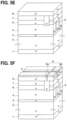
- FIG. 5 A is a perspective cross-sectional view illustrating a manufacturing process of the SiC semiconductor device shown in FIG. 2 ;
- FIG. 5 B is a perspective sectional view showing a manufacturing process of the SiC semiconductor device following FIG. 5 A ;
- FIG. 5 C is a perspective sectional view showing a manufacturing process of the SiC semiconductor device following FIG. 5 B ;
- FIG. 5 D is a perspective sectional view showing a manufacturing process of the SiC semiconductor device following FIG. 5 C ;
- FIG. 5 E is a perspective sectional view showing a manufacturing process of the SiC semiconductor device following FIG. 5 D ;
- FIG. 5 F is a perspective sectional view showing a manufacturing process of the SiC semiconductor device following FIG. 5 E ;
- FIG. 5 G is a perspective sectional view showing a manufacturing process of the SiC semiconductor device following FIG. 5 F ;
- FIG. 6 is a top view of the layout of the trench gate structure and the second deep layer described in a second embodiment
- FIG. 7 A illustrates the layout of the trench gate structure inside a semiconductor chip and a portion where the temperature is locally high
- FIG. 7 B is a top view of the semiconductor chip showing an example of the layout of the second deep layer that avoids local high temperature.
- a semiconductor device provided with a semiconductor element having a trench gate structure
- the electrical field block layer is completely depleted.
- the feedback capacitance can be increased and a change in the drain current can be reduced by an enlarging capacitance between the gate and drain. Therefore, it is possible to reduce the surge voltage and inhibit the element breakdown caused by the surge voltage.
- a p-type semiconductor for connection is used for connecting a region between the base region and the electric block layer for forming a channel region at a side surface of a trench.
- the p-type semiconductor for connection is formed to be separated from the trench by a predetermined distance.
- a shift in the forming position may occur in the formation of the p-type semiconductor through, for example, ion implantation. In this situation, for example, if the p-type semiconductor for connection is in contact with the side surface of the trench, the concentration of p-type impurities in the contact portion becomes higher than the concentration in the base region.
- the area where the MOSFET operation is performed varies depending on whether or not a shift in the forming position of the p-type semiconductor occurs and the on-resistance Ron fluctuates. Due to the shift in the forming position, the concentration of p-type impurities in the base region is substantially increased in the portion where the p-type semiconductor for connection is formed. Therefore, it may lead to an increase in the variation of the threshold voltage Vth.
- a semiconductor device includes a semiconductor element.
- the semiconductor element includes a semiconductor layer, a first-conductivity-type layer, a saturation current suppression layer, a current dispersion layer, a base region, a source region, a contact region, trench gate structures, an interlayer insulation film, a source electrode, a drain electrode and a second deep layer.
- the semiconductor layer has a first conductivity type or a second conductivity type.
- the first-conductivity-type layer is disposed above the semiconductor layer, and has the first conductivity type with an impurity concentration lower than an impurity concentration of the semiconductor layer.
- the saturation current suppression layer is above the first-conductivity-type layer.
- the saturation current suppression layer includes a first deep layer and a JFET portion.
- the first deep layer has a lengthwise direction defined as a first direction, and the first deep layer has the second conductivity type and has multiple sections aligned in a stripe pattern.
- the JFET portion has a lengthwise direction identical to the first direction, and the JFET portion has the first conductivity type.
- the JFET portion has multiple sections, which are aligned in the stripe pattern and are disposed in alternate arrangement with sections of the first deep layer.
- the current dispersion layer has the first conductivity type, and is disposed above the saturation current suppression layer.
- the base region has the second conductivity type, and is disposed above the current dispersion layer.
- the source region is disposed above the base region, and has the first conductivity type with an impurity concentration higher than the impurity concentration of the first-conductive-type layer.
- the contact region is disposed at a position different from the source region above the base region, and has the second conductivity type with an impurity concentration higher than an impurity concentration of the base region.
- the trench gate structures are aligned in a stripe pattern, and each of the trench gate structures has a lengthwise direction defined as a second direction intersecting the first direction.
- Each of the trench gate structures has a gate trench, a gate insulation film and a gate electrode.
- the gate trench penetrates the source region and the base region.
- the gate insulation film covers an inner wall surface of the gate trench.
- the gate electrode is disposed above the gate insulation film.
- the interlayer insulation film covers the gate electrode, and includes a contact hole for exposing the contact region and the source region.
- the source electrode is electrically connected to the source region through the contact hole.
- the drain electrode is disposed at a rear side of the semiconductor layer.
- the second deep layer is disposed among the trench gate structures and connected to the first deep layer.
- the second deep layer has a lengthwise direction identical to the second direction.
- the second deep layer is disposed at an entire region between adjacent two of the trench gate structures.
- the second deep layer has a width larger than or equal to a spacing between the adjacent two of the trench gate structures along a widthwise direction of each of the trench gate structures.
- the width of the second deep layer is set so that the channel region is not intentionally formed in the portion where the second deep layer is formed.
- the second deep layer is arranged at an entire region between adjacent two of the trench gate structures along the widthwise direction of the trench gate structure. Therefore, it is possible to prevent the channel region from being intentionally formed in the portion forming the second deep layer. Additionally, it is possible to suppress an increase in the on-resistance or threshold voltage due to a change in the area where the element operation is performed.
- a method manufactures a semiconductor device including a semiconductor element.
- the method includes: preparing a semiconductor layer having a first conductivity type or a second conductivity type; preparing and arranging a first-conductivity-type layer above the semiconductor layer; forming a saturation current suppression layer above the first-conductivity-type layer; forming a current dispersion layer having the first conductivity type above the saturation current suppression layer; forming a base region having the second conductivity type above the current dispersion layer; forming a source region above the base region; forming a contact region at a position different from the source region above the base region; forming trench gate structures aligned in a stripe pattern; forming an interlayer insulation film covering a gate electrode included in each of the trench gate structures; forming a source electrode electrically connected to the source region through the contact hole; forming a drain electrode at a rear side of the semiconductor layer; and forming at least one second deep layer among the plurality of trench gate structures by implanting ions
- the first-conductivity-type layer has the first conductivity type with an impurity concentration lower than an impurity concentration of the semiconductor layer.
- the saturation current suppression layer includes a first deep layer whose lengthwise direction is defined as a first direction and a JFET portion whose lengthwise direction is identical to the first direction.
- the first deep layer has the second conductivity type and has a plurality of sections aligned in a stripe pattern.
- the JFET portion has a plurality of sections aligned in the stripe pattern and disposed in alternate arrangement with the plurality of sections of the first deep layer.
- the source region has the first conductivity type with an impurity concentration higher than the impurity concentration of the first-conductive-type layer.
- the contact region has the second conductivity type with an impurity concentration higher than an impurity concentration of the base region.
- Each of the trench gate structures has a lengthwise direction defined as a second direction intersecting the first direction.
- Each of the trench gate structures includes: a gate trench that penetrates the source region and the base region; a gate insulation film that covers an inner wall surface of the gate trench; and the gate electrode that is arranged above the gate insulating film.
- the interlayer insulation film includes a contact hole for exposing the contact region and the source region.
- the second deep layer has a lengthwise direction identical to the second direction.
- the entire region has a width larger than or equal to a spacing between the adjacent two of the trench gate structures along a widthwise direction of each of the trench gate structures.
- the second deep layer is connected to the first deep layer.
- the second deep layer can be arranged in the entire region between the side walls of the adjacent gate trenches. Therefore, it is possible to form a semiconductor device in which the channel region from being intentionally formed in the portion forming the second deep layer. Additionally, it is possible to suppress an increase in the on-resistance or threshold voltage due to a change in the area where the element operation is performed.
- the present embodiment describes a SiC semiconductor device adopting silicon carbide for semiconductor material as an example. However, the present embodiment may also be applied to a semiconductor device made of the other semiconductor material such as silicon (Si).
- an inverted vertical MOSFET having a trench gate structure shown in FIGS. 1 and 2 is formed as a semiconductor device.
- the vertical MOSFET shown in those drawings is formed in a cell region of the SiC semiconductor device, and the SiC semiconductor device is configured by forming a withstand voltage maintaining structure so as to surround the cell region, but only the vertical MOSFET is shown in the drawings.
- an X-direction is orthogonal to a Y-direction
- the Y-direction is orthogonal to a Z-direction
- the Z-direction direction is orthogonal to the X-direction.
- a widthwise direction of the vertical MOSFET may be referred to as an X-direction
- a lengthwise direction of the vertical MOSFET crossing the X-direction may be referred to as a Y-direction
- a thickness direction or a depth direction of the vertical MOSFET, that is, the normal direction to the XY plane may be referred to as a Z-direction.
- FIG. 2 is a perspective cross-sectional view of a portion of a cell region, but a part of the configuration of the SiC semiconductor device is omitted in order to make the layout of each part easily understandable.
- an n + -type substrate 1 made of SiC is used as a semiconductor substrate in a SiC semiconductor device.
- An n ⁇ -type layer 2 is formed above the main surface of the n + -type substrate 1 .
- the n ⁇ -type layer 2 is included in a portion of a drift layer having a lower concentration than the n + -type substrate 1 .
- the n + -type substrate 1 corresponds to a semiconductor layer
- the n ⁇ -type layer 2 corresponds to a first-conductive-type layer.
- an n-type JFET portion 3 (hereinafter simply referred to as a JFET portion 3 ) and a p-type first deep layer 4 (hereinafter referred to as a first deep layer 4 ) included in a portion of the drift layer made of SiC are formed above the n ⁇ -type layer 2 .
- the n ⁇ -type layer 2 is connected to the JFET portion 3 at a side facing the n + -type substrate 1 .
- the JFET portion 3 and the first deep layer 4 are included in a saturation current suppression layer, and are both extended along the Y-direction as a lengthwise direction and alternately and repeatedly aligned along the X-direction.
- at least a part of the JFET portion 3 and a part of the first deep layer 4 are shaped in multiple linear shapes, that is, stripes, as viewed in a normal direction to the main surface of the n + -type substrate 1 , and are alternately arranged.
- the JFET portion 3 is formed below the first deep layer 4 .
- the stripe-shaped portions of the JFET portion 3 are connected to each other below the first deep layer 4 , but each of the stripe-shaped portions is arranged between corresponding two of the multiple sections of the first deep layer 4 .
- the first deep layer 4 is made of a p-type impurity layer.
- the first deep layer 4 has a striped shape.
- Each portion of the linear shapes of the first deep layer 4 has a constant width, and the linear shapes are arranged at an equal interval.
- the p-type impurity concentration in the depth direction is constant.
- n-type current dispersion layer 6 is formed above the JFET portion 3 and the first deep layer 4 .
- the n-type current dispersion layer 6 is included in a portion of the drift layer made of SiC.
- the n-type current dispersion layer 6 is a layer that allows a current flowing through a channel of the vertical MOSFET to spread in the Y-direction, as will be described later, and has, for example, a higher n-type impurity concentration than the n ⁇ -type layer 2 .
- the impurity concentration of the n-type current dispersion layer 6 may be identical to the impurity concentration of the n ⁇ -type layer 2 .
- the drift layer is made of the n ⁇ -type layer 2 , the JFET portion 3 and the n-type current dispersion layer 6 .
- the configuration of the drift layer may be arbitrary.
- the drift layer may include a structure having a buffer layer between the n ⁇ -type layer 2 and the n + -type substrate 1 .
- a p-type base region 7 made of SiC is formed above the n-type current dispersion layer 6 .
- An n + -type source region 8 made of SiC is formed above the p type base region 7 .
- the p-type base region 7 is set to have a lower p-type impurity concentration than the first deep layer 4 .
- the n + -type source region 8 is set to have a higher n-type impurity concentration than the n-type current dispersion layer 6 .
- a p + -type contact layer 9 is formed such that the surface of the n + -type source region 8 reaches the p-type base region 7 .
- the contact p + -type layer 9 corresponds to a contact region that is set to have a higher p-type impurity concentration than the p-type base region 7 .
- the p + -type contact layer 9 includes a coupling layer 9 a and a contact portion 9 b .
- the coupling layer 9 a is the portion having a linear shape whose lengthwise direction is along the X-direction.
- the contact portion 9 b is the portion having a linear shape whose lengthwise direction is the Y-direction intersecting the X-direction.
- a second deep layer 5 is formed below the coupling layer 9 a .
- the second deep layer 5 penetrates the p-type base region 7 and the n-type current dispersion layer 6 to connect the first deep layer 4 .
- the second deep layer 5 is formed in a linear shape with the X-direction as the longitudinal direction together with the coupling layer 9 a.
- the coupling layer 9 a and the second deep layer 5 connect the first deep layer 4 and a source electrode 14 to fix the first deep layer 4 at the source potential.
- the contact portion 9 b sets the p-type base region 7 at the source potential. If the contact portion 9 b is connected to the second deep layer 5 , the first deep layer 4 can be fixed at the source potential through the p-type base region 7 and the second deep layer 5 from the contact portion 9 b .
- the coupling layer 9 a is not essential. However, the coupling layer 9 a is provided for connecting the second deep layer 5 to the source electrode 14 in a wide region.
- the interval of forming multiple sections of the coupling layers 9 a and the interval of forming the multiple sections of second deep layer 5 are arbitrary.
- the coupling layer 9 a and the second deep layer 5 are formed in a group of several trench gate structures as one interval.
- FIG. 3 illustrates that a group of five trench gate structures in which the second deep layer 5 is disposed is formed as one interval.
- the width of the coupling layer 9 a is arbitrary. However, the width of the coupling layer 9 a is set to be shorter than or equal to the spacing between adjacent two of the trench gate structures. Similar to the second deep layer 5 , the coupling layer 9 a may also be arranged to fill the entire space between the adjacent two of the trench gate structures.
- the width of the second deep layer 5 is set to be larger than or equal to the spacing between the adjacent two of the trench gate structures. In other words, the entire region between the adjacent two of the trench gate structures along the widthwise direction of the trench gate structure, that is, the Y-direction is set to be the width of the second deep layer 5 .
- the width of the second deep layer 5 is set such that the region below the n + -type source region 8 or the coupling layer 9 a is formed as the width of the second deep layer 5 .
- the width of the second deep layer 5 is described in the following.
- the interval of forming the contact portion 9 b is also arbitrary. However, if the forming interval is too wide, a portion in the p-type base region 7 where the distance to the contact portion 9 b gets longer. Therefore, the formation interval is set so that the source potential can be reached over the entire p-type base region 7 . Since the channel density is lowered in the portion where the contact portion 9 b is formed, the forming interval of the contact portion 9 b is set to suppress a decrease in the channel density.
- the gate trench 10 is formed to penetrate the p-type base region 7 and the n + -type source region 8 to reach the n-type current dispersion layer 6 .
- the gate trench 10 has a predetermined width and a predetermined depth.
- the coupling layer 9 a is arranged also at the p-type base region 7 and the n + -type source region 8 so as to be in contact with the side surface of the gate trench 10 .
- the gate trench 10 is formed in a strip-shaped layout in which the Y-direction in FIG.
- the gate trenches 10 are formed in a stripe shape in which gate trenches 10 are arranged at equal intervals along the Y direction, and the p-type base region 7 and the n + -type source 8 are interposed therebetween. However, in a region where the second deep layer 5 is formed, the p-type base region 7 between the gate trenches 10 is replaced with the second deep layer 5 .
- the spacing between the trench gate structures in other words, the spacing Pt between the side surface of the gate trench 10 and the side surface of the adjacent gate trench 10 is arbitrary.
- the spacing Pt may also be referred to as a distance between the side surface of the gate trench 10 and the side surface of the adjacent gate trench.
- the spacing Pt is set to be narrowed as 2 micrometers or shorter.
- the spacing Pt is set to be 1 micrometer or shorter.
- the width Wt of the gate trench 10 is arbitrary.
- the width Wt is set to be smaller than the distance between the center position of the trench gate structure and the center position of the adjacent trench gate structure.
- the width Wt is set to be in a range of 0.5 micrometer to 0.8 micrometer.
- the spacing between the adjacent two of the gate trenches 10 is a value obtained by subtracting the width Wt from a cell pitch.
- the gate trenches 10 are formed in a stripe shape as viewed in a direction normal to the main surface of the n + -type substrate 1 , in other words, as viewed from above.
- the gate trenches may also be formed to have a least one portion formed in the stripe shape.
- two adjacent gate trenches 10 with linear shape may be set as a group, and the gate trenches 10 may be laid out so that both ends of the gate trenches 10 are connected in a semicircular shape.
- a portion of the p-type base region 7 located at the side surface of the gate trench 10 is a channel region connecting the n + -type source region 8 and the n-type current dispersion layer 6 when the vertical MOSFET is operated.
- the inner wall surface of the trench 10 is covered with the gate insulating film 11 .
- a gate electrode 12 made of doped Poly-Si is formed on a surface of the gate insulating film 11 , and the gate trench 10 is filled with the gate insulating film 11 and the gate electrode 12 to form a trench gate structure.
- An interlayer insulating film 13 is formed so as to cover the gate electrode 12 .
- the interlayer insulating film 13 may extend outside the gate trench 10 . However, in the present embodiment, the interlayer insulating film 13 is disposed inside the gate trench 10 , and the gate trench 10 is filled by the gate insulating film 11 , the gate electrode 12 and the interlayer insulating film 13 .
- a source electrode 14 and the like are formed on the surface of the n + -type source region 8 and the surface of the gate electrode 12 via the interlayer insulating film 13 .
- the source electrode 14 is made of multiple metals, for example, Ni/AI or the like. Among multiple metals, a portion that is in contact with at least the n-type SiC, specifically, the n + -type source region 8 and the gate electrode 12 in the case of n-type doping, is made of a metal capable of ohmic contact with the n-type SiC.
- At least a portion contacting with, among the multiple metals, at least the p-type SiC, specifically, a portion contacting with the p + -type contact layer 9 is made of a metal capable of ohmic contact with the p-type SiC.
- the source electrode 14 is formed on the interlayer insulating film 13 and is electrically insulated from the SiC portion, but is electrically in contact with the n ⁇ -type source region 8 and the p + -type contact layer 9 through the contact holes formed in the interlayer insulating film 13 .
- a drain electrode 15 electrically connected to the n ⁇ -type substrate 1 is formed on a rear surface of the n + -type substrate 1 .
- the vertical MOSFET of an n-channel inverted type trench gate structure is provided.
- a cell region is formed by placing the vertical MOSFET cells described above.
- the SiC semiconductor device including the vertical MOSFET configured as described above is operated by, for example, applying a gate voltage Vg of 20 V to the gate electrode 12 in a state where the source voltage Vs is 0 V and the drain voltage Vd is 1 to 1.5 V. That is, when the gate voltage Vg is applied, the vertical MOSFET performs an operation in which a channel region is formed in a portion of the p-type base region 7 that contacts with the gate trench 10 and a current flows between the drain and the source.
- the JFET portion 3 and the first deep layer 4 function as a saturation current suppression layer, and it is possible to maintain a low saturation current while achieving a low on-state resistance by providing a saturation current suppression effect. Specifically, since the stripe shaped portions of the JFET portion 3 and the first deep layer 4 are alternately formed repeatedly, the following operation is performed.
- the depletion layer extending from the first deep layer 4 to the JFET portion 3 extends only to a width smaller than the width of the stripe shaped portion of the JFET portion 3 . For that reason, even if the depletion layer extends into the JFET portion 3 , a current path is secured. If the n ⁇ -type impurity concentration of the JFET portion 3 is set to be higher than the concentration of the n ⁇ -type layer 2 , it is possible that the current path can be configured to have a low resistance, and a low on-resistance can be achieved.
- the depletion layer extending from the first deep layer 4 to the JFET portion 3 extends more than the width of the stripe shaped portion of the JFET portion 3 . Then, the JFET portion 3 is immediately pinched off before the n-type current dispersion layer 6 . As a result, it is possible to maintain a low saturation current and enhance the withstand capacity of the SiC semiconductor device due to, for example, a load short circuit.
- the JFET portion 3 and the first deep layer 4 function as a saturation current suppression layer, and exhibit a saturation current suppression effect, thereby providing a SiC semiconductor device that can achieve both low on-state resistance and low saturation current.
- the stripe shaped portions of the JFET portion 3 and the first deep layer 4 are alternately and repeatedly formed. Therefore, even when the drain voltage Vd becomes a high voltage, the extension of the depletion layer extending from the bottom to the n ⁇ -type layer 2 is suppressed by the first deep layer 4 . Thus, it may be possible to prevent the depletion layer from extending into the trench gate structure. Therefore, an electric field control effect for lowering the electric field applied to the gate insulating film 11 can be exhibited, and the gate insulating film 11 can be inhibited from being broken, so that a highly reliable element with high withstand voltage can be obtained.
- the extension of the depletion layer to the trench gate structure can be prevented as described above, the n-type impurity concentration of the n-type layer 2 and the JFET portion 3 can be made relatively high, and a low on-resistance can be achieved.
- the SiC semiconductor device having a vertical MOSFET with low on-resistance and high reliability can be provided.
- the SiC semiconductor device in the present embodiment includes the semiconductor element of a normally-off type in which no current flows between the drain and the source when the gate voltage Vg is not applied, since the channel region is not formed.
- the JFET portion 3 is of a normally-on type because it pinches off only when the drain voltage Vd is higher than the voltage during normal operation, even in the case of non-application of the gate voltage Vg.
- the SiC semiconductor device according to the present embodiment can perform the operation described above accurately.
- the second deep layer 5 is included when the first deep layer 4 is fixed to the source potential. However, it is typically considered that the channel region is formed at a position where the second deep layer 5 is formed. As illustrated in FIG. 4 A , the width of the second deep layer 5 is shorter than the spacing Pt between adjacent gate trenches 10 , and the p-type base region 7 is inverted at the side surface of the trench gate structure located at both sides of the second deep layer 5 and the channel region is formed.
- the area where the MOSFET operation is performed varies depending on whether or not the shift in the forming position of the p-type semiconductor occurs and the on-resistance Ron fluctuates. Due to the shift in the forming position, the concentration of p-type impurities in the p-type base region 7 is substantially increased around the portion where the second deep layer 5 is formed. Therefore, it leads to an increase in the variation of the threshold voltage Vth.
- the width of the second deep layer 5 in other words, the dimension in the Y-direction is set such that the channel is not intentionally formed in the portion where the second deep layer 5 is formed and the MOSFET operation is not performed in that portion.
- the width Wp of the second deep layer 5 is set to be larger than or equal to the spacing Pt between the gate trenches 10 .
- the second deep layer 5 is disposed at the entire region between the side walls of the adjacent gate trenches 10 along the Y-direction. Therefore, it is possible to prevent the channel region from being intentionally formed in the portion forming the second deep layer 5 . Additionally, it is possible to suppress an increase in the on-resistance or threshold voltage due to a change in the area where the MOSFET operation is performed.
- the width Wp of the second deep layer 5 may be set to a dimension in consideration of the shift in the forming position of the second deep layer 5 .
- the width Wp of the second deep layer 5 may be set to the dimension obtained by adding the deviation amount D of the forming position to the spacing Pt between the gate trenches 10 .
- the width Wp of the second deep layer 5 may be set to satisfy the mathematical relation of Pt+D ⁇ Wp.
- the width Wp of the second deep layer 5 is set to be shorter than the sum of the respective widths Wt of the two gate trenches 10 and the spacing Pt between the adjacent gate trenches 10 .
- the width Wp may be set to satisfy the mathematical relation of Wp ⁇ Pt+2Wt.
- the width Wp of the second deep layer 5 may be set to satisfy the mathematical relation of Wp ⁇ Pt+2Wt-D, in consideration of the deviation amount D of the forming position of the second deep layer 5 .
- the shift in the forming position of the second deep 5 does not refer to the misalignment with reference to an alignment mark (not shown) in the formation of the second deep layer 5 , it refers to the misalignment of the second deep layer 5 with respect to the gate electrode 10 .
- the misalignment of the formation of the gate trench 10 may also occur, both of the misalignment of the formation of the second deep layer 5 and the misalignment of the formation of the gate trench 10 affects a shift in the relative position of the second deep layer 5 with respect to the gate trench 10 .
- the width Wp of the second deep layer 5 is set based on the maximum value of both of the positional shift of the formation of the gate trench 10 and the positional shift of the formation of the second deep layer 5 as the deviation amount D. However, it is not necessary to take into consideration of the deviation amount D as the maximum value of the shift in the forming position. It is sufficient to set the width Wp of the second deep layer 5 in consideration of the deviation amount D.
- the n + -type substrate 1 made of, for example, SiC is prepared as a semiconductor substrate.
- an n ⁇ -type layer 2 made of SiC is formed on the main surface of the n + -type substrate 1 by epitaxial growth using a CVD (chemical vapor deposition) apparatus (not shown).
- a so-called epitaxial substrate in which the n ⁇ -type layer 2 is grown in advance on the main surface of the n + -type substrate 1 may be used.
- the JFET portion 3 made of SiC is epitaxially grown on the n ⁇ -type layer 2 .
- the first deep layer 4 is formed at a predetermined region of the JFET portion 3 .
- a mask 17 made of an oxide film or the like is disposed on a surface of the JFET portion 3 , the mask 17 is patterned to open a region where the first deep layer 4 is to be formed. Then, the p-type impurity is ion-implanted to form the first deep layer 4 . Thereafter, the mask 17 is removed.
- the first deep layer 4 is formed by ion implantation in this example, the first deep layer 4 may be formed by a method other than ion implantation.
- the JFET portion 3 is selectively anisotropically etched to form a recess portion at a position corresponding to the first deep layer 4 , a p-type impurity layer is epitaxially grown on the concave portion, and then the p-type impurity layer is flattened at a portion located on the JFET portion 3 to form the first deep layer 4 .
- the first deep layer 4 can also be formed by epitaxial growth.
- n-type SiC is epitaxially grown on the JFET portion 3 and the first deep layer 4 to form the n-type current dispersion layer 5 .
- the p-type base region 7 is epitaxially grown on the n-type current dispersion layer 6 .
- n + -type source region 8 is epitaxially grown on the second deep layer 5 and the p-type base region 7 .
- a mask 19 having an opening corresponding to the p + -type contact layer 9 is formed on the n + -type source region 8 .
- the p + -type contact layer 9 including the coupling layer 9 a and the contact portion 9 b is formed through ion-implantation of p-type impurity by using the mask 19 . Thereafter, the mask 19 is removed.
- the gate trench 10 is formed by performing anisotropic etching process such as RIE using a mask.
- the deposition of the oxide film or thermal oxidation is performed to form the gate insulating film 11 , so that the gate insulation film 11 covers an inner wall surface of the gate trench 10 and the surface of the n + -type source region 8 .
- a Poly-Si doped with a p-type impurity or an n-type impurity is deposited, and then etched back to leave the Poly-Si in the gate trench 10 , thereby forming the gate electrode 12 .
- the trench gate structure is completed.
- the interlayer insulating film 13 made of, for example, an oxide film is formed so as to cover the surfaces of the gate electrode 12 and the gate insulating film 11 .
- the interlayer insulating film 13 is etched with a mask (not shown) until the n + -type source region 8 and the p + -type contact layer 9 are exposed, and the contact hole is formed and the interlayer insulating film 13 inside the gate trench gate 13 remains.
- the following processes are performed. Then, after the electrode material provided by, for example, a laminated structure of multiple metals is formed on the surface of the interlayer insulation film 13 , the source electrode 14 is formed by patterning the electrode material. Furthermore, the drain electrode 15 is formed on the back side of the n + -type substrate 1 . In this manner, the SiC semiconductor device according to the present embodiment is completed.
- the width of the second deep layer 5 in other words, the dimension in the Y-direction is set, such that the channel is not intentionally formed in the portion where the second deep layer 5 is formed and the MOSFET operation is not performed in that portion.
- the width Wp of the second deep layer 5 is set to be larger than or equal to the spacing Pt between the adjacent two of the gate trenches 10 .
- the second deep layer 5 is disposed at the entire region between the respective side walls of the adjacent two of the gate trenches 10 in the Y-direction. Therefore, it is possible to prevent the channel region from being intentionally formed in the portion forming the second deep layer 5 . Additionally, it is possible to suppress an increase in the on-resistance or threshold voltage due to a change in the area where the MOSFET operation is performed.
- the width Wp of the second deep layer 5 is set to be shorter than the sum of the widths Wt of the adjacent two of the gate trenches 10 and the spacing Pt between the adjacent two of the gate trenches 10 .
- the width Wp may be set to satisfy the mathematical relation of Wp ⁇ Pt+2Wt.
- the present embodiment is a modification in which the layout of the second deep layer 5 is changed from the first embodiment, and similar to the first embodiment except the modified part, so that only portions different from those in the first embodiment will be described.
- each of the multiple sections of the second deep layer 5 is formed among a group of several trench gate structures as one interval.
- each of the multiple sections of the second deep layer 5 is disposed among a group of five trench gate structures, such that the formation density of the multiple sections of the second deep layer 5 inside the cell region is uniform.
- the multiple sections of the second deep layer 5 are disposed at equal intervals inside the cell region.
- the multiple sections of second deep layer 5 are respectively formed among several groups of the trench gate structures while the multiple sections of second deep layer 5 are disposed at unequal intervals.
- a first one of the multiple sections of second deep layer 5 is placed among a group of three trench gate structures
- a second one of the multiple sections of second deep layer 5 is among a group of five trench gate structures
- a third one of the multiple sections of second deep layer 5 is placed among a group of eight trench gate structures.
- a third embodiment will be described.
- the present embodiment is a modification in which the forming position of the second deep layer 5 is changed from the first embodiment, and similar to the first embodiment except the modified part, so that only portions different from those in the first embodiment will be described.
- the center of the cell region tends to have a high temperature, and the temperature gradually decreases as deviated from the center of the cell region.
- the heat is dissipated toward the outer peripheral side of the cell region.
- the heat cannot be easily dissipated and is concentrated in the center of the cell region.
- the density of disposing the multiple sections of second deep layer 5 at a portion where the temperature tends to be high is increased to suppress the deviation of temperature inside the cell region.
- a first one of the multiple sections of second deep layer 5 is arranged in a circular shape at the center of the cell region.
- a second one of the multiple sections of second deep layer 5 and a third one of the multiple sections of second deep layer 5 are arranged concentrically around the center of the cell region.
- the arrangement interval of the multiple sections of second deep layer 5 is widened as deviated from the center of the cell region.
- the first deep layer 4 is formed by forming the first deep layer 4 with an ion-implanted layer. In other words, the first deep layer 4 is formed through the ion-implantation of the p-type impurity after the formation of the JFET portion 3 .
- the JFET portion 3 may be formed by forming the JFET portion 3 with an ion-implanted layer. In other words, the JFET portion 3 may be formed through ion-implantation of the n-type impurity subsequent to the epitaxial growth of the first deep layer 4 above the n ⁇ -type layer 2 .
- the section between adjacent two gate trenches 10 is made as the second deep layer 5 .
- the section across three or more consecutive gate trenches 10 may be made as the second deep layer 5 .
- the channel region cannot be formed at two or more regions between the adjacent gate trenches 10 , it is possible to increase the current density per unit area in the structure according to the first embodiment.
- the second deep layer 5 is formed through ion-implantation of the p-type base region 7 and the n-type current dispersion layer 6 from the surface of the p-type base region 7 . Additionally, the coupling layer 9 a and the contact portion 9 b are formed at the same time. Such a manufacturing method is particularly effective when a semiconductor material such as SiC in which the injected ions are not diffused by heat treatment is used.
- the coupling layer 9 a and the contact portion 9 b may be separately formed, and the coupling layer 9 a and the second deep layer 5 may be formed at the same time by using a mask disposed at the surface of the n + -type source region 8 .
- the n + -type substrate 1 as a semiconductor layer is prepared, and the n ⁇ -type layer 2 corresponding to the n-type conductivity type layer is epitaxially grown on the n + -type substrate 1 .
- the above method is merely an example.
- the n ⁇ -type layer 2 may be used as the semiconductor substrate, and the semiconductor layer may be formed to have a higher impurity concentration than the n ⁇ -type layer 2 by implanting ions at the rear surface of the n ⁇ -type layer 2 .
- an n channel-type vertical MOSFET in which the first conductivity type is n-type and the second conductivity type is p-type has been described as an example.
- the conductivity type of each element may be reversed so as to form a p-channel type vertical MOSFET.
- the vertical MOSFET is described as an example of the semiconductor element.
- the present disclosure may also be applied to an IGBT having a similar structure.
- the conductivity type of the n + -type substrate 1 is changed from the n-type substrate to the p-type substrate in each of the above embodiments, and the structures and manufacturing methods are the same as those in each of the above embodiments, except that the conductivity type of the n + -type substrate 1 is changed from the n-type substrate to the p-type substrate.
- the trench gate structure is described as an example in the present description, a planar type MOSFET or IGBT may be adopted, and an element other than MOSFET and IGBT may also be adopted.
Landscapes
- Electrodes Of Semiconductors (AREA)
Abstract
Description
Claims (7)
Applications Claiming Priority (2)
| Application Number | Priority Date | Filing Date | Title |
|---|---|---|---|
| JP2021-090106 | 2021-05-28 | ||
| JP2021090106A JP7574743B2 (en) | 2021-05-28 | 2021-05-28 | Semiconductor device and its manufacturing method |
Publications (2)
| Publication Number | Publication Date |
|---|---|
| US20220384621A1 US20220384621A1 (en) | 2022-12-01 |
| US11967634B2 true US11967634B2 (en) | 2024-04-23 |
Family
ID=84156793
Family Applications (1)
| Application Number | Title | Priority Date | Filing Date |
|---|---|---|---|
| US17/824,236 Active 2042-06-14 US11967634B2 (en) | 2021-05-28 | 2022-05-25 | Semiconductor device and method of manufacturing the same |
Country Status (3)
| Country | Link |
|---|---|
| US (1) | US11967634B2 (en) |
| JP (1) | JP7574743B2 (en) |
| CN (1) | CN115411111A (en) |
Families Citing this family (1)
| Publication number | Priority date | Publication date | Assignee | Title |
|---|---|---|---|---|
| DE112023004913T5 (en) * | 2022-12-28 | 2025-09-18 | Rohm Co., Ltd. | SIC semiconductor component |
Citations (2)
| Publication number | Priority date | Publication date | Assignee | Title |
|---|---|---|---|---|
| US20190157437A1 (en) * | 2017-02-24 | 2019-05-23 | Fuji Electric Co., Ltd. | Semiconductor device |
| JP2020109808A (en) | 2019-01-07 | 2020-07-16 | 株式会社デンソー | Semiconductor device |
Family Cites Families (7)
| Publication number | Priority date | Publication date | Assignee | Title |
|---|---|---|---|---|
| US6392273B1 (en) | 2000-01-14 | 2002-05-21 | Rockwell Science Center, Llc | Trench insulated-gate bipolar transistor with improved safe-operating-area |
| US20030209741A1 (en) * | 2002-04-26 | 2003-11-13 | Wataru Saitoh | Insulated gate semiconductor device |
| JP4623956B2 (en) * | 2003-11-12 | 2011-02-02 | 株式会社豊田中央研究所 | IGBT |
| WO2015151185A1 (en) | 2014-03-31 | 2015-10-08 | 新電元工業株式会社 | Semiconductor device |
| WO2017047286A1 (en) * | 2015-09-16 | 2017-03-23 | 富士電機株式会社 | Semiconductor device |
| JP6825520B2 (en) * | 2017-09-14 | 2021-02-03 | 三菱電機株式会社 | Semiconductor devices, semiconductor device manufacturing methods, power conversion devices |
| JP7180402B2 (en) * | 2019-01-21 | 2022-11-30 | 株式会社デンソー | semiconductor equipment |
-
2021
- 2021-05-28 JP JP2021090106A patent/JP7574743B2/en active Active
-
2022
- 2022-05-25 US US17/824,236 patent/US11967634B2/en active Active
- 2022-05-26 CN CN202210585166.9A patent/CN115411111A/en active Pending
Patent Citations (2)
| Publication number | Priority date | Publication date | Assignee | Title |
|---|---|---|---|---|
| US20190157437A1 (en) * | 2017-02-24 | 2019-05-23 | Fuji Electric Co., Ltd. | Semiconductor device |
| JP2020109808A (en) | 2019-01-07 | 2020-07-16 | 株式会社デンソー | Semiconductor device |
Also Published As
| Publication number | Publication date |
|---|---|
| US20220384621A1 (en) | 2022-12-01 |
| CN115411111A (en) | 2022-11-29 |
| JP7574743B2 (en) | 2024-10-29 |
| JP2022182509A (en) | 2022-12-08 |
Similar Documents
| Publication | Publication Date | Title |
|---|---|---|
| US11063145B2 (en) | Silicon carbide semiconductor device and method for manufacturing same | |
| US11476360B2 (en) | Semiconductor device and method for manufacturing the same | |
| US8193564B2 (en) | Silicon carbide semiconductor device including deep layer | |
| US10516046B2 (en) | Silicon carbide semiconductor device | |
| JP2020119939A (en) | Semiconductor device | |
| US11538935B2 (en) | Silicon carbide semiconductor device | |
| US10714611B2 (en) | Silicon carbide semiconductor device | |
| US20220246719A1 (en) | Silicon carbide semiconductor device and method of manufacturing the same | |
| CN110291620A (en) | Semiconductor device and method for manufacturing semiconductor device | |
| US20240079492A1 (en) | Semiconductor device | |
| EP4510194A1 (en) | Semiconductor device and method for producing same | |
| US12426319B2 (en) | Semiconductor device and method for manufacturing the same | |
| US20250351473A1 (en) | Semiconductor device and method for manufacturing the same | |
| JP7585740B2 (en) | Semiconductor Device | |
| US11967634B2 (en) | Semiconductor device and method of manufacturing the same | |
| CN112466924A (en) | Silicon carbide semiconductor device and method for manufacturing silicon carbide semiconductor device | |
| JP7439746B2 (en) | silicon carbide semiconductor device | |
| JP2020109809A (en) | Semiconductor device | |
| US11366022B2 (en) | Semiconductor device having a temperature sensor | |
| JP7127315B2 (en) | Silicon carbide semiconductor device and manufacturing method thereof | |
| JP7673513B2 (en) | Semiconductor Device | |
| US20260047154A1 (en) | Silicon carbide semiconductor device | |
| EP4432364A1 (en) | Semiconductor device | |
| JP2023114354A (en) | Switching device and manufacturing method thereof | |
| CN121003031A (en) | silicon carbide semiconductor devices |
Legal Events
| Date | Code | Title | Description |
|---|---|---|---|
| FEPP | Fee payment procedure |
Free format text: ENTITY STATUS SET TO UNDISCOUNTED (ORIGINAL EVENT CODE: BIG.); ENTITY STATUS OF PATENT OWNER: LARGE ENTITY |
|
| STPP | Information on status: patent application and granting procedure in general |
Free format text: DOCKETED NEW CASE - READY FOR EXAMINATION |
|
| AS | Assignment |
Owner name: MIRISE TECHNOLOGIES CORPORATION, JAPAN Free format text: ASSIGNMENT OF ASSIGNORS INTEREST;ASSIGNORS:NAGATA, KENSUKE;IWAHASHI, YOHEI;SUZUKI, RYOTA;AND OTHERS;SIGNING DATES FROM 20220609 TO 20220613;REEL/FRAME:060407/0686 Owner name: TOYOTA JIDOSHA KABUSHIKI KAISHA, JAPAN Free format text: ASSIGNMENT OF ASSIGNORS INTEREST;ASSIGNORS:NAGATA, KENSUKE;IWAHASHI, YOHEI;SUZUKI, RYOTA;AND OTHERS;SIGNING DATES FROM 20220609 TO 20220613;REEL/FRAME:060407/0686 Owner name: DENSO CORPORATION, JAPAN Free format text: ASSIGNMENT OF ASSIGNORS INTEREST;ASSIGNORS:NAGATA, KENSUKE;IWAHASHI, YOHEI;SUZUKI, RYOTA;AND OTHERS;SIGNING DATES FROM 20220609 TO 20220613;REEL/FRAME:060407/0686 |
|
| STPP | Information on status: patent application and granting procedure in general |
Free format text: NON FINAL ACTION MAILED |
|
| STPP | Information on status: patent application and granting procedure in general |
Free format text: RESPONSE TO NON-FINAL OFFICE ACTION ENTERED AND FORWARDED TO EXAMINER |
|
| STPP | Information on status: patent application and granting procedure in general |
Free format text: EX PARTE QUAYLE ACTION MAILED |
|
| STPP | Information on status: patent application and granting procedure in general |
Free format text: RESPONSE TO EX PARTE QUAYLE ACTION ENTERED AND FORWARDED TO EXAMINER |
|
| STPP | Information on status: patent application and granting procedure in general |
Free format text: NOTICE OF ALLOWANCE MAILED -- APPLICATION RECEIVED IN OFFICE OF PUBLICATIONS |
|
| ZAAB | Notice of allowance mailed |
Free format text: ORIGINAL CODE: MN/=. |
|
| STPP | Information on status: patent application and granting procedure in general |
Free format text: PUBLICATIONS -- ISSUE FEE PAYMENT VERIFIED |
|
| STCF | Information on status: patent grant |
Free format text: PATENTED CASE |