US11922905B2 - Display device and method for displaying an image thereon - Google Patents
Display device and method for displaying an image thereon Download PDFInfo
- Publication number
- US11922905B2 US11922905B2 US17/833,770 US202217833770A US11922905B2 US 11922905 B2 US11922905 B2 US 11922905B2 US 202217833770 A US202217833770 A US 202217833770A US 11922905 B2 US11922905 B2 US 11922905B2
- Authority
- US
- United States
- Prior art keywords
- image
- movement path
- time
- period
- display device
- Prior art date
- Legal status (The legal status is an assumption and is not a legal conclusion. Google has not performed a legal analysis and makes no representation as to the accuracy of the status listed.)
- Active
Links
Images


Classifications
-
- G—PHYSICS
- G09—EDUCATION; CRYPTOGRAPHY; DISPLAY; ADVERTISING; SEALS
- G09G—ARRANGEMENTS OR CIRCUITS FOR CONTROL OF INDICATING DEVICES USING STATIC MEANS TO PRESENT VARIABLE INFORMATION
- G09G5/00—Control arrangements or circuits for visual indicators common to cathode-ray tube indicators and other visual indicators
- G09G5/36—Control arrangements or circuits for visual indicators common to cathode-ray tube indicators and other visual indicators characterised by the display of a graphic pattern, e.g. using an all-points-addressable [APA] memory
- G09G5/38—Control arrangements or circuits for visual indicators common to cathode-ray tube indicators and other visual indicators characterised by the display of a graphic pattern, e.g. using an all-points-addressable [APA] memory with means for controlling the display position
-
- G—PHYSICS
- G06—COMPUTING OR CALCULATING; COUNTING
- G06T—IMAGE DATA PROCESSING OR GENERATION, IN GENERAL
- G06T3/00—Geometric image transformations in the plane of the image
- G06T3/20—Linear translation of whole images or parts thereof, e.g. panning
-
- G—PHYSICS
- G09—EDUCATION; CRYPTOGRAPHY; DISPLAY; ADVERTISING; SEALS
- G09G—ARRANGEMENTS OR CIRCUITS FOR CONTROL OF INDICATING DEVICES USING STATIC MEANS TO PRESENT VARIABLE INFORMATION
- G09G3/00—Control arrangements or circuits, of interest only in connection with visual indicators other than cathode-ray tubes
- G09G3/007—Use of pixel shift techniques, e.g. by mechanical shift of the physical pixels or by optical shift of the perceived pixels
-
- G—PHYSICS
- G09—EDUCATION; CRYPTOGRAPHY; DISPLAY; ADVERTISING; SEALS
- G09G—ARRANGEMENTS OR CIRCUITS FOR CONTROL OF INDICATING DEVICES USING STATIC MEANS TO PRESENT VARIABLE INFORMATION
- G09G3/00—Control arrangements or circuits, of interest only in connection with visual indicators other than cathode-ray tubes
- G09G3/20—Control arrangements or circuits, of interest only in connection with visual indicators other than cathode-ray tubes for presentation of an assembly of a number of characters, e.g. a page, by composing the assembly by combination of individual elements arranged in a matrix no fixed position being assigned to or needed to be assigned to the individual characters or partial characters
- G09G3/22—Control arrangements or circuits, of interest only in connection with visual indicators other than cathode-ray tubes for presentation of an assembly of a number of characters, e.g. a page, by composing the assembly by combination of individual elements arranged in a matrix no fixed position being assigned to or needed to be assigned to the individual characters or partial characters using controlled light sources
- G09G3/28—Control arrangements or circuits, of interest only in connection with visual indicators other than cathode-ray tubes for presentation of an assembly of a number of characters, e.g. a page, by composing the assembly by combination of individual elements arranged in a matrix no fixed position being assigned to or needed to be assigned to the individual characters or partial characters using controlled light sources using luminous gas-discharge panels, e.g. plasma panels
-
- G—PHYSICS
- G09—EDUCATION; CRYPTOGRAPHY; DISPLAY; ADVERTISING; SEALS
- G09G—ARRANGEMENTS OR CIRCUITS FOR CONTROL OF INDICATING DEVICES USING STATIC MEANS TO PRESENT VARIABLE INFORMATION
- G09G3/00—Control arrangements or circuits, of interest only in connection with visual indicators other than cathode-ray tubes
- G09G3/20—Control arrangements or circuits, of interest only in connection with visual indicators other than cathode-ray tubes for presentation of an assembly of a number of characters, e.g. a page, by composing the assembly by combination of individual elements arranged in a matrix no fixed position being assigned to or needed to be assigned to the individual characters or partial characters
- G09G3/22—Control arrangements or circuits, of interest only in connection with visual indicators other than cathode-ray tubes for presentation of an assembly of a number of characters, e.g. a page, by composing the assembly by combination of individual elements arranged in a matrix no fixed position being assigned to or needed to be assigned to the individual characters or partial characters using controlled light sources
- G09G3/30—Control arrangements or circuits, of interest only in connection with visual indicators other than cathode-ray tubes for presentation of an assembly of a number of characters, e.g. a page, by composing the assembly by combination of individual elements arranged in a matrix no fixed position being assigned to or needed to be assigned to the individual characters or partial characters using controlled light sources using electroluminescent panels
- G09G3/32—Control arrangements or circuits, of interest only in connection with visual indicators other than cathode-ray tubes for presentation of an assembly of a number of characters, e.g. a page, by composing the assembly by combination of individual elements arranged in a matrix no fixed position being assigned to or needed to be assigned to the individual characters or partial characters using controlled light sources using electroluminescent panels semiconductive, e.g. using light-emitting diodes [LED]
- G09G3/3208—Control arrangements or circuits, of interest only in connection with visual indicators other than cathode-ray tubes for presentation of an assembly of a number of characters, e.g. a page, by composing the assembly by combination of individual elements arranged in a matrix no fixed position being assigned to or needed to be assigned to the individual characters or partial characters using controlled light sources using electroluminescent panels semiconductive, e.g. using light-emitting diodes [LED] organic, e.g. using organic light-emitting diodes [OLED]
- G09G3/3225—Control arrangements or circuits, of interest only in connection with visual indicators other than cathode-ray tubes for presentation of an assembly of a number of characters, e.g. a page, by composing the assembly by combination of individual elements arranged in a matrix no fixed position being assigned to or needed to be assigned to the individual characters or partial characters using controlled light sources using electroluminescent panels semiconductive, e.g. using light-emitting diodes [LED] organic, e.g. using organic light-emitting diodes [OLED] using an active matrix
- G09G3/3233—Control arrangements or circuits, of interest only in connection with visual indicators other than cathode-ray tubes for presentation of an assembly of a number of characters, e.g. a page, by composing the assembly by combination of individual elements arranged in a matrix no fixed position being assigned to or needed to be assigned to the individual characters or partial characters using controlled light sources using electroluminescent panels semiconductive, e.g. using light-emitting diodes [LED] organic, e.g. using organic light-emitting diodes [OLED] using an active matrix with pixel circuitry controlling the current through the light-emitting element
-
- G—PHYSICS
- G09—EDUCATION; CRYPTOGRAPHY; DISPLAY; ADVERTISING; SEALS
- G09G—ARRANGEMENTS OR CIRCUITS FOR CONTROL OF INDICATING DEVICES USING STATIC MEANS TO PRESENT VARIABLE INFORMATION
- G09G3/00—Control arrangements or circuits, of interest only in connection with visual indicators other than cathode-ray tubes
- G09G3/20—Control arrangements or circuits, of interest only in connection with visual indicators other than cathode-ray tubes for presentation of an assembly of a number of characters, e.g. a page, by composing the assembly by combination of individual elements arranged in a matrix no fixed position being assigned to or needed to be assigned to the individual characters or partial characters
- G09G3/34—Control arrangements or circuits, of interest only in connection with visual indicators other than cathode-ray tubes for presentation of an assembly of a number of characters, e.g. a page, by composing the assembly by combination of individual elements arranged in a matrix no fixed position being assigned to or needed to be assigned to the individual characters or partial characters by control of light from an independent source
- G09G3/36—Control arrangements or circuits, of interest only in connection with visual indicators other than cathode-ray tubes for presentation of an assembly of a number of characters, e.g. a page, by composing the assembly by combination of individual elements arranged in a matrix no fixed position being assigned to or needed to be assigned to the individual characters or partial characters by control of light from an independent source using liquid crystals
-
- G—PHYSICS
- G09—EDUCATION; CRYPTOGRAPHY; DISPLAY; ADVERTISING; SEALS
- G09G—ARRANGEMENTS OR CIRCUITS FOR CONTROL OF INDICATING DEVICES USING STATIC MEANS TO PRESENT VARIABLE INFORMATION
- G09G2320/00—Control of display operating conditions
- G09G2320/02—Improving the quality of display appearance
- G09G2320/0257—Reduction of after-image effects
-
- G—PHYSICS
- G09—EDUCATION; CRYPTOGRAPHY; DISPLAY; ADVERTISING; SEALS
- G09G—ARRANGEMENTS OR CIRCUITS FOR CONTROL OF INDICATING DEVICES USING STATIC MEANS TO PRESENT VARIABLE INFORMATION
- G09G2320/00—Control of display operating conditions
- G09G2320/04—Maintaining the quality of display appearance
- G09G2320/043—Preventing or counteracting the effects of ageing
- G09G2320/046—Dealing with screen burn-in prevention or compensation of the effects thereof
-
- G—PHYSICS
- G09—EDUCATION; CRYPTOGRAPHY; DISPLAY; ADVERTISING; SEALS
- G09G—ARRANGEMENTS OR CIRCUITS FOR CONTROL OF INDICATING DEVICES USING STATIC MEANS TO PRESENT VARIABLE INFORMATION
- G09G2320/00—Control of display operating conditions
- G09G2320/10—Special adaptations of display systems for operation with variable images
- G09G2320/106—Determination of movement vectors or equivalent parameters within the image
Definitions
- Embodiments of the present invention relate to a display device, and a method for displaying an image thereon.
- display devices include organic light emitting display devices, liquid crystal display devices, and plasma display devices.
- a pixel may deteriorate as a driving time increases, which degrades the function thereof. For example, in the case of a display device that continuously outputs a same image for a long period of time, pixel deterioration may be accelerated, such that image sticking may occur.
- the display device may move an image (e.g., a predetermined image) 20 displayed in an image display region 10 according to a movement path (e.g., a predetermined movement path).
- a movement path e.g., a predetermined movement path
- the portion of the image display region 10 that does not include the image 20 may be displayed in black.
- the image 20 may be moved without weighting (e.g., without varying the display time of the image 20 at each position included in the movement path).
- an x-axis and a y-axis may indicate a region of the image display region 10 in which the image 20 exists, and a z-axis may indicate a weighted value at each corresponding position.
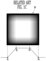
- FIG. 1 C Considering an accumulated image 30 during a period of time (e.g., a predetermined period of time) illustrated in FIG. 1 C , there may be formed regions V 1 , V 2 , V 3 and V 4 in which a grayscale is dramatically changed, and portions corresponding to the regions V 1 , V 2 , V 3 and V 4 may be recognized by the user as image sticking.
- Embodiments of the present invention relate to a display device capable of reducing a phenomenon of image sticking by giving a weighted value depending on a position of an image, and a method for displaying an image thereon.
- Embodiments of the present invention also relate to a method for displaying an image, the method including moving the image displayed on an image display region along a movement path including a first position and a second position during a period of time, wherein, during the period of time, a total time for which the image is located at the first position is greater than a total time for which the image is located at the second position.
- the second position may be located at a greater distance from a center point of the image display region than the first position.
- the image may stay at the first position for a first individual time, and may stay at the second position for a second individual time that is less than the first individual time.
- a number of times for which the image is located at the first position may be greater than a number of times for which the image is located at the second position.
- the image may stay at the first position for a first individual time, and may stay at the second position for a second individual time that is the same as the first individual time.
- the movement path may include an initial position, a final position, and a plurality of intermediate positions including the first position and the second position between the initial position and the final position on the movement path.
- the image may reciprocate along the movement path from the initial position to the final position.
- the intermediate positions may further include a first intermediate position and a second intermediate position, and the image may reciprocate along the movement path from the initial position to the second intermediate position after reciprocating along the movement path from the initial position to the first intermediate position.
- the second intermediate position may be located at a greater distance from a center point of the image display region than the first intermediate position.
- the second intermediate position may be located at a shorter distance from a center point of the image display region than the first intermediate position.
- the movement path may include a shape spiraling around the initial position.
- Embodiments of the present invention also relate to a method for displaying an image on a display device, the method including moving the image displayed on an image display region along a movement path including a first position and a second position during a period of time, wherein the second position is located at a greater distance from a center point of the image display region than the first position, wherein the image located at the first position is given a weighted value that is higher than a weighted value given to the image located at the second position, and wherein the weighted value corresponds to individual time for which the image is located at the first position and the second position, respectively, or a number of times for which the image is located at the first position and the second position during the period of time.
- Embodiments of the present invention also relate to a display device, the display device including a display panel including an image display region in which a plurality of pixels are located, a display driver for displaying an image on the image display region, and a movement path provider for providing a movement path including a first position and a second position to the display driver, wherein the display driver is configured to move an image displayed in the image display region along the movement path during a period of time, and wherein a total time for which the image is located at the first position during the period of time is greater than a total time for which the image is located at the second position during the period of time.
- the movement path provider may further include a memory for storing image movement information, and a coordinate generator for generating coordinate information for each position in the movement path with reference to the image movement information.
- the image movement information may correspond to a movement direction of the image.
- the second position may be located at a greater distance from a center point of the image display region than the first position.
- the display driver may be configured to keep the image at the first position for a first individual time, and to keep the image at the second position for a second individual time that is less than the first individual time.
- a number of times that the image is located at the first position may be greater than a number of times that the image is located at the second position during the period of time.
- the display driver may be configured to keep the image at the first position for a first individual time, and to keep the image at the second position for a second individual time that is the same as the first individual time.
- the movement path may include an initial position, a final position, and a plurality of intermediate positions including the first position and the second position and located between the initial position and the final position.
- the display driver may be configured to reciprocate the image along the movement path from the initial position to the final position.
- the intermediate positions may include a first intermediate position and a second intermediate position
- the display driver may be configured to reciprocate the image along the movement path from the initial position to the second intermediate position after reciprocating the image along the movement path from the initial position to the first intermediate position.
- the second intermediate position may be located at a greater distance from a center point of the image display region than the first intermediate position.
- the second intermediate position may be located at a shorter distance from a center point of the image display region than the first intermediate position.
- the movement path may include a shape spiraling around the initial position.
- Each of the pixels may include an organic light emitting diode.
- FIGS. 1 A to 1 C illustrate conventional pixel shift technology
- FIG. 2 illustrates an image display region of a display device in accordance with an embodiment of the present invention
- FIG. 3 illustrates a method for displaying an image in accordance with an embodiment of the present invention
- FIGS. 4 A to 4 D illustrate a weighting method in accordance with an embodiment of the present invention
- FIG. 5 illustrates a movement path of an image in accordance with an embodiment of the present invention
- FIG. 6 illustrates a movement path of an image in accordance with another embodiment of the present invention.
- FIG. 7 illustrates a movement path of an image in accordance with yet another embodiment of the present invention.
- FIG. 8 illustrates a display device in accordance with an embodiment of the present invention
- FIG. 9 illustrates a display driving unit (e.g., a display driver) and a display panel in accordance with an embodiment of the present invention
- FIG. 10 illustrates an embodiment of a pixel illustrated in FIG. 9 ;
- FIG. 11 illustrates a movement path provider in accordance with an embodiment of the present invention.
- FIG. 12 illustrates an embodiment of a lookup table stored in a memory of FIG. 11 in accordance with an embodiment of the present invention.
- spatially relative terms such as “beneath,” “below,” “lower,” “under,” “above,” “upper,” and the like, may be used herein for ease of explanation to describe one element or feature's relationship to another element(s) or feature(s) as illustrated in the figures. It will be understood that the spatially relative terms are intended to encompass different orientations of the device in use or in operation, in addition to the orientation depicted in the figures. For example, if the device in the figures is turned over, elements described as “below” or “beneath” or “under” other elements or features would then be oriented “above” the other elements or features. Thus, the example terms “below” and “under” can encompass both an orientation of above and below. The device may be otherwise oriented (e.g., rotated 90 degrees or at other orientations) and the spatially relative descriptors used herein should be interpreted accordingly.
- the x-axis, the y-axis and the z-axis are not limited to three axes of a rectangular coordinate system, and may be interpreted in a broader sense.
- the x-axis, the y-axis, and the z-axis may be perpendicular to one another, or may represent different directions that are not perpendicular to one another.
- the term “substantially,” “about,” and similar terms are used as terms of approximation and not as terms of degree, and are intended to account for the inherent deviations in measured or calculated values that would be recognized by those of ordinary skill in the art. Further, the use of “may” when describing embodiments of the present invention refers to “one or more embodiments of the present invention.” As used herein, the terms “use,” “using,” and “used” may be considered synonymous with the terms “utilize,” “utilizing,” and “utilized,” respectively. Also, the term “exemplary” is intended to refer to an example or illustration.
- a specific process order may be performed differently from the described order.
- two consecutively described processes may be performed substantially at the same time or performed in an order opposite to the described order.
- the electronic or electric devices and/or any other relevant devices or components according to embodiments of the present invention described herein may be implemented utilizing any suitable hardware, firmware (e.g. an application-specific integrated circuit), software, or a combination of software, firmware, and hardware.
- the various components of these devices may be formed on one integrated circuit (IC) chip or on separate IC chips.
- the various components of these devices may be implemented on a flexible printed circuit film, a tape carrier package (TCP), a printed circuit board (PCB), or formed on one substrate.
- the various components of these devices may be a process or thread, running on one or more processors, in one or more computing devices, executing computer program instructions and interacting with other system components for performing the various functionalities described herein.
- the computer program instructions are stored in a memory which may be implemented in a computing device using a standard memory device, such as, for example, a random access memory (RAM).
- the computer program instructions may also be stored in other non-transitory computer readable media such as, for example, a CD-ROM, flash drive, or the like.
- a person of skill in the art should recognize that the functionality of various computing devices may be combined or integrated into a single computing device, or the functionality of a particular computing device may be distributed across one or more other computing devices without departing from the spirit and scope of the exemplary embodiments of the present invention.
- FIG. 2 illustrates an image display region of a display device in accordance with an embodiment of the present invention
- FIG. 3 illustrates a method for displaying an image in accordance with an embodiment of the present invention.
- a display device 200 in accordance with an embodiment of the present invention may include an image display region/display area DA that displays the image.
- the display device 200 may provide a user with an image Im (e.g., a predetermined image), and may display the image Im using pixels in the image display region DA. Accordingly, the user of the display device 200 may see the image Im displayed in the image display region DA.
- an image Im e.g., a predetermined image
- the display device 200 may be used in a television, a monitor, a mobile device, a navigation device, etc.
- FIG. 2 illustrates the image Im positioned at a center point Cp of the image display region DA.
- a pixel shift technology that displays the image Im by moving the image Im to reduce image sticking may be used.
- the image Im may be moved in the image display region DA according to a movement path (e.g., a predetermined movement path) during a period of time (e.g., a pixel shift period)
- the image Im may be located in the first position P 1 at least once during the pixel shift period, and may be located in the second position P 2 at least once during the pixel shift period.
- image sticking may be reduced by varying weighted values according to the position of the image Im.
- a first position that is closer to the center point Cp of the image display region DA may have a higher weighted value in comparison to a second position that is farther away from the center point Cp than the first location.
- weighted values may be set according to the amount of time for which the image is located at each associated position during the pixel shift period.
- the weighted value associated with the first position P 1 which is closer than the second position P 2 to the center point Cp of the image display region DA, may be set to a higher number than the weighted value associated with the second position P 2 .
- the weighted value associated with the second position P 2 which is located farther away from the center point Cp in the image display region DA than the first position P 1 , may be a lower number than the weighted value associated with the first position P 1 .
- a total amount of time for which the image Im is located at the first position P 1 during the pixel shift period may be greater than a total amount of time for which the image Im is located at the second position P 2 .
- an individual time for which the image Im stays at each position included in the movement path may be adjusted, or the number of times for which, during the pixel shift period, the image Im stays at each position included in the movement path may be adjusted.
- weighted values may be controlled by these two methods (i.e., adjusting the individual time for which the image Im stays at each position, or adjusting the number of times for which the image Im stays at each position).
- FIGS. 4 A to 4 D illustrate a weighting method in accordance with an embodiment of the present invention
- the weighted values may be represented using a parabolic shape or a paraboloid, or may be represented using a curved portion of a sine wave.
- an x-axis and a y-axis may show a position (e.g., a coordinate) at which the image Im is located in the image display region DA, and a z-axis may show the weighted value at each position.
- FIG. 4 B illustrates accumulated image 310 at the image display region DA, which is generated during the period of time (e.g., the pixel shift period) when the weighted value is represented by the shape shown in FIG. 4 A .
- a higher, first weighted value may be associated with a center portion of the image display region DA, and weighted values associated with other positions may decrease as the distance between the positions and the center portion increases (i.e., as the image Im moves toward an outside/edge of the display region DA).
- the weighted value set for each position in the image display region DA may be represented together by a parabolic shape in which the center portion is represented by a curved upper portion, as illustrated in FIG. 4 A .
- the accumulated image 310 for the pixel shift period may be shown as illustrated in FIG. 4 B , and a grayscale of the accumulated image 310 may be gradually changed (e.g., see regions R 1 , R 2 , R 3 and R 4 ).
- a grayscale of the accumulated image 310 may be gradually changed (e.g., see regions R 1 , R 2 , R 3 and R 4 ).
- image sticking may be reduced, so that the display device may provide natural images with the user.
- the weighted values associated with each position included in the image display region DA may be represented by a polygon that includes slopes (e.g., may be pyramid-shaped).
- the higher, first weighted value may be associated with the center portion of the image display region DA, and lower weighted values associated with other positions may decrease as the distance between a corresponding one of the other positions and the center portion increases.
- the weighted values may decrease (e.g., decrease linearly) as the distance between the associated position and the center portion of the image display region DA increase. That is, the weighted values may decrease as the image Im moves away from the center portion of the image display region DA.
- the weighted values associated with each of the positions in the image display region DA may be represented as a shape having steps/stair-like formations.
- discontinuity of the weighted values may be more distinct in comparison with the weighted values illustrated in FIGS. 4 A and 4 C . That is, discontinuity of the weighted values may be higher in FIG. 4 D than in FIGS. 4 A and 4 C .
- weighting method may vary in other embodiments.
- another weighting method may associate increasing weighted values as the distance between the position and the center portion of the image display region DA increases (e.g., as the image Im is farther away from the center portion of the image display region DA) may be employed as the method for displaying the image in accordance with an embodiment of the present invention.
- FIG. 5 illustrates a movement path of an image Im in accordance with an embodiment of the present invention.
- the image Im e.g., a center of the image Im
- the image Im located at an initial position Ip and the image Im located at a final position Fp.
- a movement path Pa 1 in accordance with an embodiment of the present invention may be represented by a zigzag-like shape. Accordingly, in the method for displaying the image in accordance with the present embodiment, the image Im may move along the movement path Pa 1 illustrated in FIG. 5 during a period of time (e.g., the pixel shift time).
- a period of time e.g., the pixel shift time
- the image Im may move along the movement path Pa 1 from a first side (e.g., an upper side) to another side (e.g., a lower side) while travelling from left to right and from right to left.
- the movement path Pa 1 may include the initial position Ip, the final position Fp, and a plurality of intermediate positions M 1 to M 28 located between the initial position Ip and the final position Fp on the movement path Pa 1 . Accordingly, the image Im may move from the initial position Ip to the final position Fp through the intermediate positions M 1 to M 28 .
- the image Im may also move from the final position Fp to the initial position Ip through the intermediate positions M 1 to M 28 .
- the image Im may repeatedly move between the initial position Ip and the final position Fp along the movement path Pa 1 during the pixel shift period.
- an individual time for which the image Im stays at each position included in the movement path Pa 1 may be adjusted.
- the image Im may stay at the second intermediate position M 2 for a time A, may stay at the seventh intermediate position M 7 for a time B, and may stay at the twelfth intermediate position M 12 for a time C.
- a relation of magnitude among the time A, the time B and the time C may be expressed as follows. time A ⁇ time B ⁇ time C
- the image Im when the image Im moves along the movement path Pa 1 four times (e.g., reciprocates along the movement path Pa 1 twice) during the pixel shift period, the image Im may be located at each of the intermediate positions M 2 , M 7 , and M 12 four times. Accordingly, a total amount of time for which the image Im is located at the second intermediate position M 2 during the pixel shift period may be represented as a time 4 A (e.g., four times time A). Similarly, a total amount of time for which the image Im is located at the seventh intermediate position M 7 and at the twelfth intermediate position M 12 during the pixel shift period may be represented as a time 4 B and a time 4 C, respectively.
- a time 4 A e.g., four times time A
- a total amount of time for which the image Im is located at the seventh intermediate position M 7 and at the twelfth intermediate position M 12 during the pixel shift period may be represented as a time 4 B and a time 4 C, respectively.
- the weighted values may vary according to the position of the image Im by adjusting the individual time for which the image Im stays at each position.
- the movement path Pa 1 illustrated in FIG. 5 does not cross the center point Cp of the image display region DA (e.g., the center point Cp is out of the movement path Pa 1 as an example).
- the center point Cp of the image display region DA may be located on/within the movement path Pa 1 .
- the center point Cp of the image display region DA may be located at, or may be consistent with, one of the intermediate positions M 1 to M 28 .
- FIG. 5 illustrates twenty-eight intermediate positions (e.g., intermediate positions M 1 to M 28 ) as an example, the number of intermediate positions may vary (e.g., may vary depending on a length of the movement path Pa 1 ).
- the image Im may move a distance of one pixel at a time. For example, when an amount of movement of the image Im is set to one pixel, the image Im located at the initial position Ip may move to the first intermediate position M 1 by moving the image Im one pixel to the right.
- FIG. 6 illustrates a movement path of an image in accordance with another embodiment of the present invention.
- the image Im e.g., the center of the image Im
- the image Im located at the initial position Ip and the image Im located at the final position Fp.
- a movement path Pa 2 in accordance with another embodiment of the present invention may be represented by a zigzag-like shape.
- the movement path Pa 2 illustrated in FIG. 6 may be represented by the same shape used to represent the movement path Pa 1 illustrated in FIG. 5 , although the same shape is rotated 90 degrees.
- the image Im may move along the movement path Pa 2 from one side (e.g., a left side) to another side (e.g., a right side) by moving up and down.
- FIG. 7 illustrates a movement path of an image Im in accordance with yet another embodiment of the present invention.
- the image Im e.g., the center of the image Im
- the image Im located at the final position Fp e.g., the image Im located at the final position Fp.
- a movement path Pa 3 in accordance with another embodiment of the present invention may be represented by a spiral-like shape around the initial position Ip.
- the movement path Pa 3 may include a spiral shape spiraling away from the center position Cp of the image display region DA.
- the movement path Pa 3 may include the initial position Ip, the final position Fp, and a plurality of intermediate positions M 1 to M 40 arranged between the initial position Ip and the final position Fp on the movement path Pa 3 .
- the initial position Ip may be located at the center point Cp of the image display region DA.
- the image Im may repeatedly move between the initial position Ip and the final position Fp along the movement path Pa 3 during the pixel shift period.
- the image Im may move from the initial position Ip to the final position Fp through the intermediate positions M 1 to M 40 , and may move back to the initial position Ip through the intermediate positions M 40 to M 1 .
- an individual time for which the image Im stays at each position included in the movement path Pa 3 may be adjusted.
- the image Im may stay at the fifth intermediate position M 5 for a time E, may stay at the eighteenth intermediate position M 18 for a time F, and may stay at the thirty-ninth intermediate position M 39 for a time G.
- a relation of magnitude among the time E, the time F and the time G may be expressed as follows. time E>time F>time G
- the image Im when the image Im moves along the movement path Pa 3 four times (e.g., reciprocates along the movement path Pa 3 twice) during the pixel shift period, the image Im may be located at each intermediate position M 5 , M 18 , and M 39 four times. Accordingly, a total amount of time for which the image Im is located at the fifth intermediate position M 5 during the pixel shift period may be represented as a time 4 E (i.e., four times the time E). In addition, a total amount of time for which the image Im is located at the eighteenth intermediate position M 18 and at the thirty-ninth intermediate position M 39 during the pixel shift period may be represented as a time 4 F and a time 4 G, respectively.
- the weighted values may vary according to the position of the image Im by adjusting the individual time for which the image Im stays at each position.
- the weighted value may be adjusted by a method using a portion of the movement path Pa 3 during the pixel shift period instead of a method in which the image Im repeatedly moves between the initial position Ip and the final position Fp along the movement path Pa 3 .
- the image may move from the initial position Ip to the twentieth intermediate position M 20 and may then move back to the initial position Ip along the movement path Pa 3 .
- the image may move from the initial position Ip to the sixth intermediate position M 6 , and may move back to the initial position Ip along the movement path Pa 3 .
- the number of positions at which the image Im is located may differ depending on the number of positions included in the movement path Pa 3 .
- the image may be located at the fifth intermediate position M 5 three times, at the eighteenth intermediate position M 18 twice, and at the thirty-ninth intermediate position M 39 once during the pixel shift period.
- a total amount of time for which the image Im is located at the fifth intermediate position M 5 which is closer to the center point Cp of the image display region DA than intermediate positions M 18 and M 39 , may be larger than the total amount of time for which the image Im is located at each of intermediate positions M 18 and M 39 .
- a total amount of time for which the image Im is located at the thirty-ninth intermediate position M 39 which is farther from the center point Cp of the image display region DA than intermediate positions M 5 and M 18 , may be less than the total amount of time for which the image Im is located at each of intermediate positions M 5 and M 18 .
- weighted values may vary according to the position of the image Im by adjusting the number of positions included in the movement path Pa 3 at which the image Im is located.
- the image Im may move from the initial position Ip to the final position Fp, and may then move back to the initial position Ip along the movement path Pa 3 , although movement of the image Im may vary.
- the image Im may then move from the initial position Ip to the twentieth intermediate position M 20 , and then back to the initial position Ip along the movement path Pa 3 .
- the image Im may then move from the initial position Ip to the twentieth intermediate position M 20 , and then back to the initial position Ip along the movement path Pa 3 .
- FIGS. 5 to 7 illustrate various movement paths Pa 1 , Pa 2 , and Pa 3 as examples, the movement path of the image Im may be varied.
- FIG. 8 illustrates a display device in accordance with an embodiment of the present invention
- the display device 200 in accordance with an embodiment of the present invention may include a display panel 400 , a display driver 500 , and a movement path provider 600 .
- the display panel 400 may include a plurality of pixels P (as shown in FIG. 9 ), to thereby display an image (e.g., a predetermined image).
- the display panel 400 may include an image display region/display area DA (as shown in FIG. 9 ) in which the plurality of pixels P are located. Accordingly, the display panel 400 may display the image at the image display region DA according to control information provided by the display driver 500 .
- the display panel 400 may be embodied by an organic light emitting display panel, but the display panel 400 is not limited thereto.
- the display driver 500 may control an image display operation of the display panel 400 by supplying a driving signal Dd to the display panel 400 .
- the display driver 500 may move an image displayed at the image display region DA of the display panel 400 along the movement path Pa provided from the movement path provider 600 for a period of time (e.g., a pixel shift period).
- the display driver 500 may increase the reduction of image sticking by setting the weighted values according to the position included in the movement path Pa. Because a method of setting the weighted value is already described in detail above, the description will be omitted.
- the movement path provider 600 may provide the movement path Pa of the image to the display driver 500 .
- the movement path Pa may include coordinate information of the positions constituting a path Pa.
- the movement path provider 600 may be separated from the display driver 500 as described in FIG. 8 .
- the movement path provider 600 may be integrated with the display driver 500 .
- FIG. 9 illustrates a display driving unit (e.g., the display driver) and a display panel in accordance with an embodiment of the present invention.
- a display driving unit e.g., the display driver
- the display panel 400 in accordance with an embodiment of the present invention may include a plurality of data lines D 1 to Dm, a plurality of scan lines S 1 to Sn, and a plurality of pixels P.
- the pixels P may be connected to the data lines D 1 to Dm and the scan lines S 1 to Sn.
- the pixels P may be arranged at respective crossing regions of the data lines D 1 to Dm and the scan lines S 1 to Sn in a matrix configuration.
- each pixel P may receive a data signal and a scan signal through respective ones of the data lines D 1 to Dm and the scan lines S 1 to Sn.
- the display driver 500 may include a scan driver 510 , a data driver 520 and a timing controller 550 .
- the driving signal Dd of the display driver 500 may include the scan signal and the data signal.
- the scan driver 510 may supply the scan signals to the scan lines S 1 to Sn corresponding to a scan driver control signal SCS. For example, the scan driver 510 may sequentially provide the scan signals to the scan lines S 1 to Sn.
- the scan driver 510 may be electrically connected to the scan lines S 1 to Sn located at the display panel 400 through a separate component (e.g., a circuit board). In another embodiment, the scan driver 510 may be directly mounted in the display panel 400 .
- the data driver 520 may receive a data driver control signal DCS and image data DATA from the timing controller 550 , and may generate the data signal.
- the data driver 520 may supply a generated signal to the data lines D 1 to Dm.
- the data driver 520 may be electrically connected to the data lines D 1 to Dm located in the display panel 400 through a separate component (e.g., a circuit substrate). In another embodiment, the data driver 520 may be directly mounted in the display panel 400 .
- a partial group of pixels P connected to a specific scan line may receive the data signal transmitted from the data lines D 1 to Dm, and the group of pixels P may emit light with the brightness corresponding to the supplied data signal.
- the timing controller 550 may generate control signals to control the scan driver 510 and the data driver 520 .
- the control signals may include the scan driver control signal SCS to control the scan driver 510 , and may include the data driver control signal DSC to control the data driver 520 .
- the timing controller 550 may supply the scan driver control signal SCS to the scan driver 510 , and may supply the data driver control signal DSC to the data driver 520 .
- the timing controller 550 may convert the data DATA according to specifications of the data driver 520 , and may supply the data DATA to the data driver 520 . In addition, the timing controller 550 may control the scan driver 510 and the data driver 520 so that the image displayed in the image display region DA may move along the movement path Pa supplied from the movement path provider 600 .
- FIG. 10 illustrates an embodiment of a pixel illustrated in FIG. 9 .
- FIG. 10 illustrates a pixel P connected to an n th scan line Sn and an m th data line Dm.
- the pixel P may include an organic light emitting diode (OLED) and a pixel circuit 700 connected to the data line Dm and the scan line Sn to control the OLED.
- OLED organic light emitting diode
- An anode electrode of the OLED may be connected to the pixel circuit 700 , and a cathode electrode of the OLED may be connected to a second power ELVSS.
- the OLED may generate light (e.g., light of a predetermined luminance) corresponding to a current supplied from the pixel circuit 700 .
- the pixel circuit 700 may store the data signal supplied to an m th data line Dm when the scan signal is supplied to an n th scan line Sn, and may control current volume supplied to the OLED corresponding to the stored data signal.
- the pixel circuit 700 may include a first transistor T 1 , a second transistor T 2 , and a storage capacitor Cst.
- the first transistor T 1 may be connected between the m th data line Dm and the second transistor T 2 .
- a gate electrode of the first transistor T 1 may be connected to an n th scan line Sn
- a first electrode of the first transistor T 1 may be connected to an m th data line Dm
- a second electrode of the first transistor T 1 may be connected to a gate electrode of the second transistor T 2 .
- the first transistor T 1 may turn on when the scan signal is supplied from the n th scan line Sn, and may supply the data signal from the m th data line Dm to the storage capacitor Cst.
- the storage capacitor Cst may charge a voltage corresponding to the data signal.
- the second transistor T 2 may be connected between a first power ELVDD and the OLED.
- the gate electrode of the second transistor T 2 may be connected to the first electrode of the storage capacitor Cst and to the second electrode of the first transistor T 1
- the first electrode of the second transistor T 2 may be connected to the second electrode of the storage capacitor Cst and to the first power ELVDD
- the second electrode of the second transistor T 2 may be connected to the anode electrode of the OLED.
- the second transistor T 2 may, as a driving transistor, control the current volume flowing from the first power ELVDD to the second power ELVSS via the OLED corresponding to a voltage value stored in the storage capacitor Cst.
- the OLED may generate the light corresponding to the current volume supplied from the second transistor T 2 .
- the first electrode of the transistors T 1 and T 2 may be set as one of the source electrode and the drain electrode, and the second electrode of the transistors T 1 and T 2 may be set to a different electrode from the first electrode.
- the second electrode may be the drain electrode.
- the pixel P of the present invention is not limited to the pixel structure.
- the pixel circuit 700 has a circuit structure that supplies the current to the OLED, and the pixel circuit 700 may be selected as any one of a variety of suitable structures.
- FIG. 11 illustrates a movement path provider in accordance with an embodiment of the present invention.
- FIG. 12 illustrates an embodiment of a lookup table stored in a memory in FIG. 11 in accordance with an embodiment of the present invention.
- the movement path provider 600 in accordance with an embodiment of the present invention may include a memory 610 and a coordinate generator 620 .
- the memory 610 may store image movement information Inf.
- the image movement information Inf may include a movement direction SD.
- the memory 610 may include the image movement information Inf in a lookup table LUT configuration illustrated in FIG. 12 .
- the look-up table LUT may include an up, a down, a left, and a right movement direction SD.
- the coordinate generator 620 may generate the movement path Pa with reference to the image movement information Inf stored in the memory 610 .
- the movement path Pa may include the coordinate information indicating the position.
- an image Im (e.g., a predetermined image) may be displayed at the initial position Ip in the image display area DA.
- the coordinate generator 620 may sequentially refer to the movement direction SD from the image movement information Inf stored in the memory 610 . For example, because a first movement direction of the image movement information Inf is a right movement direction, the coordinate generator 620 may calculate the coordinate (1, 0) indicating the first intermediate position M 1 (e.g., the coordinate of the initial position Ip is assumed to be (0, 0)).
- the coordinate generator 620 may calculate the coordinate (1, ⁇ 1) indicating the second intermediate position M 2 . In the same way, the coordinate generator 620 may sequentially calculate the coordinates/coordinate points indicating the remaining intermediate positions M 3 to M 40 and the final position Fp.
- the coordinates calculated by the coordinate generator 620 may constitute the movement path Pa, and may be delivered to the display driver 500 .
- the display driver 500 receives the coordinate (1, 0) from the coordinate generator 620 , the image Im displayed at the initial position Ip may move to the first intermediate position M 1 .
- the display driver 500 when the display driver 500 receives the coordinate (1, ⁇ 1) from the coordinate generator 620 , the image Im illustrated at the first intermediate position M 1 may move to the second intermediate position M 2 . In the same manner, the display driver 500 may move the image Im along the movement path Pa 3 during the pixel shift period.
- the display driver 500 may maintain the current position of the image Im.
- an individual time for which the image Im stays at a particular position may be adjusted.
- the present invention may provide a display device that reduces image sticking by varying a weighted value according to a position of an image and a method for displaying an image thereof.
Landscapes
- Engineering & Computer Science (AREA)
- Physics & Mathematics (AREA)
- General Physics & Mathematics (AREA)
- Theoretical Computer Science (AREA)
- Computer Hardware Design (AREA)
- Chemical & Material Sciences (AREA)
- Crystallography & Structural Chemistry (AREA)
- Plasma & Fusion (AREA)
- Control Of Indicators Other Than Cathode Ray Tubes (AREA)
- Control Of El Displays (AREA)
Abstract
Description
time A<time B<time C
time E>time F>time G
Claims (20)
Priority Applications (2)
| Application Number | Priority Date | Filing Date | Title |
|---|---|---|---|
| US17/833,770 US11922905B2 (en) | 2016-01-28 | 2022-06-06 | Display device and method for displaying an image thereon |
| US18/412,340 US12361915B2 (en) | 2016-01-28 | 2024-01-12 | Display device and method for displaying an image thereon |
Applications Claiming Priority (6)
| Application Number | Priority Date | Filing Date | Title |
|---|---|---|---|
| KR1020160010815A KR102537608B1 (en) | 2016-01-28 | 2016-01-28 | Display device and method for displaying image thereof |
| KR10-2016-0010815 | 2016-01-28 | ||
| US15/365,829 US10147401B2 (en) | 2016-01-28 | 2016-11-30 | Display device and method for displaying an image thereon |
| US16/175,655 US10783855B2 (en) | 2016-01-28 | 2018-10-30 | Display device and method for displaying an image thereon |
| US17/027,593 US11355090B2 (en) | 2016-01-28 | 2020-09-21 | Display device and method for displaying an image thereon |
| US17/833,770 US11922905B2 (en) | 2016-01-28 | 2022-06-06 | Display device and method for displaying an image thereon |
Related Parent Applications (1)
| Application Number | Title | Priority Date | Filing Date |
|---|---|---|---|
| US17/027,593 Continuation US11355090B2 (en) | 2016-01-28 | 2020-09-21 | Display device and method for displaying an image thereon |
Related Child Applications (1)
| Application Number | Title | Priority Date | Filing Date |
|---|---|---|---|
| US18/412,340 Continuation US12361915B2 (en) | 2016-01-28 | 2024-01-12 | Display device and method for displaying an image thereon |
Publications (2)
| Publication Number | Publication Date |
|---|---|
| US20220301524A1 US20220301524A1 (en) | 2022-09-22 |
| US11922905B2 true US11922905B2 (en) | 2024-03-05 |
Family
ID=59386216
Family Applications (5)
| Application Number | Title | Priority Date | Filing Date |
|---|---|---|---|
| US15/365,829 Active 2036-12-10 US10147401B2 (en) | 2016-01-28 | 2016-11-30 | Display device and method for displaying an image thereon |
| US16/175,655 Active US10783855B2 (en) | 2016-01-28 | 2018-10-30 | Display device and method for displaying an image thereon |
| US17/027,593 Active US11355090B2 (en) | 2016-01-28 | 2020-09-21 | Display device and method for displaying an image thereon |
| US17/833,770 Active US11922905B2 (en) | 2016-01-28 | 2022-06-06 | Display device and method for displaying an image thereon |
| US18/412,340 Active US12361915B2 (en) | 2016-01-28 | 2024-01-12 | Display device and method for displaying an image thereon |
Family Applications Before (3)
| Application Number | Title | Priority Date | Filing Date |
|---|---|---|---|
| US15/365,829 Active 2036-12-10 US10147401B2 (en) | 2016-01-28 | 2016-11-30 | Display device and method for displaying an image thereon |
| US16/175,655 Active US10783855B2 (en) | 2016-01-28 | 2018-10-30 | Display device and method for displaying an image thereon |
| US17/027,593 Active US11355090B2 (en) | 2016-01-28 | 2020-09-21 | Display device and method for displaying an image thereon |
Family Applications After (1)
| Application Number | Title | Priority Date | Filing Date |
|---|---|---|---|
| US18/412,340 Active US12361915B2 (en) | 2016-01-28 | 2024-01-12 | Display device and method for displaying an image thereon |
Country Status (3)
| Country | Link |
|---|---|
| US (5) | US10147401B2 (en) |
| KR (3) | KR102537608B1 (en) |
| CN (2) | CN114220396B (en) |
Families Citing this family (18)
| Publication number | Priority date | Publication date | Assignee | Title |
|---|---|---|---|---|
| KR102537608B1 (en) * | 2016-01-28 | 2023-05-30 | 삼성디스플레이 주식회사 | Display device and method for displaying image thereof |
| US10475417B2 (en) * | 2017-03-29 | 2019-11-12 | Intel Corporation | History-aware selective pixel shifting |
| CN107016961B (en) * | 2017-06-07 | 2019-09-17 | 京东方科技集团股份有限公司 | Image display method, storage medium, image drive and display device |
| KR102348651B1 (en) * | 2017-11-21 | 2022-01-07 | 엘지전자 주식회사 | Organic light emitting diode display device and method for operating thereof |
| WO2019139539A1 (en) * | 2018-01-12 | 2019-07-18 | 新加坡能源创新发展有限公司 | Data transmission system and method |
| JP6950551B2 (en) * | 2018-02-01 | 2021-10-13 | セイコーエプソン株式会社 | Image display device and its control method |
| CN110363209B (en) * | 2018-04-10 | 2022-08-09 | 京东方科技集团股份有限公司 | Image processing method, image processing apparatus, display apparatus, and storage medium |
| CN108810321A (en) * | 2018-06-28 | 2018-11-13 | 深圳市华星光电半导体显示技术有限公司 | Image processing method and device |
| KR102571750B1 (en) * | 2018-10-04 | 2023-08-28 | 삼성디스플레이 주식회사 | Display device and method for displaying image using display device |
| KR102648198B1 (en) * | 2019-01-14 | 2024-03-19 | 삼성디스플레이 주식회사 | Afterimage compensator and display device having the same |
| JP7391552B2 (en) * | 2019-06-27 | 2023-12-05 | エルジー ディスプレイ カンパニー リミテッド | Display control device and display control method |
| KR102760598B1 (en) * | 2019-11-04 | 2025-02-04 | 삼성디스플레이 주식회사 | Display device and driving method thereof |
| KR102788092B1 (en) * | 2020-09-18 | 2025-04-01 | 삼성디스플레이 주식회사 | Display device and driving method of display device |
| KR102708859B1 (en) * | 2020-11-09 | 2024-09-24 | 엘지디스플레이 주식회사 | Display device and image processing method thereof |
| CN117529766A (en) * | 2021-07-09 | 2024-02-06 | 三星电子株式会社 | Display device and control method thereof |
| EP4322143A4 (en) | 2021-07-09 | 2024-08-07 | Samsung Electronics Co., Ltd. | DISPLAY DEVICE AND CONTROL METHOD THEREFOR |
| US12002408B2 (en) | 2021-11-19 | 2024-06-04 | Samsung Display Co., Ltd. | Display device in which reference point is shifted in shift area based on route shift signal |
| KR20240164667A (en) | 2023-05-11 | 2024-11-20 | 삼성디스플레이 주식회사 | Display device and electronic device |
Citations (16)
| Publication number | Priority date | Publication date | Assignee | Title |
|---|---|---|---|---|
| US20040051705A1 (en) | 2002-09-17 | 2004-03-18 | Lg Electronics Inc. | Display system and method of eliminating residual image in the same |
| KR100451745B1 (en) | 2002-09-17 | 2004-10-08 | 엘지전자 주식회사 | A display device and method for preventing an afterimage screen of the same |
| US20050204313A1 (en) | 2004-03-09 | 2005-09-15 | Pioneer Corporation | Display screen burn prevention method |
| KR100551052B1 (en) | 2003-11-19 | 2006-02-09 | 삼성에스디아이 주식회사 | Method and apparatus for preventing afterimage of plasma panel, plasma display panel having apparatus |
| EP1720148A2 (en) | 2005-05-02 | 2006-11-08 | Semiconductor Energy Laboratory Co., Ltd. | Display device and gray scale driving method with subframes thereof |
| US20080111886A1 (en) | 2006-11-13 | 2008-05-15 | Samsung Electronics Co., Ltd | Image display device and method thereof |
| CN101183295A (en) | 2006-11-16 | 2008-05-21 | 国际商业机器公司 | Method for displaying image on display screen |
| US20110134316A1 (en) | 2009-12-08 | 2011-06-09 | Canon Kabushiki Kaisha | Image display apparatus and method |
| CN102243840A (en) | 2010-05-10 | 2011-11-16 | 三星移动显示器株式会社 | Organic light emitting display device and method for driving thereof |
| CN102467865A (en) | 2010-11-18 | 2012-05-23 | 深圳Tcl新技术有限公司 | A method for preventing screen burn-in of flat panel display |
| US20120236040A1 (en) * | 2011-03-18 | 2012-09-20 | Samsung Electronics Co. Ltd. | Method and apparatus for providing graphical user interface |
| CN102903346A (en) | 2008-02-19 | 2013-01-30 | 奇菱科技股份有限公司 | Liquid crystal display device and method for improving picture flicker and picture ghost |
| US20150077406A1 (en) * | 2013-09-17 | 2015-03-19 | Samsung Display Co., Ltd. | Display device and method for driving the same |
| US20150154910A1 (en) | 2013-11-29 | 2015-06-04 | Samsung Display Co., Ltd. | Display device, method of calculating compensation data thereof, and driving method thereof |
| US20160267627A1 (en) | 2014-03-24 | 2016-09-15 | Boe Techology Group Co., Ltd. | Display system and driving method thereof |
| US20170221455A1 (en) | 2016-01-28 | 2017-08-03 | Samsung Display Co., Ltd. | Display device and method for displaying an image thereon |
Family Cites Families (5)
| Publication number | Priority date | Publication date | Assignee | Title |
|---|---|---|---|---|
| EP1489589A4 (en) * | 2002-03-04 | 2009-11-04 | Sanyo Electric Co | Organic electroluminescence display and its application |
| CN1947409A (en) * | 2004-04-22 | 2007-04-11 | 精工爱普生株式会社 | Image processor for multivalue conversion in units of pixels |
| KR20060065277A (en) * | 2004-12-10 | 2006-06-14 | 삼성전자주식회사 | Display device and control method |
| JP2008058346A (en) * | 2006-08-29 | 2008-03-13 | Seiko Epson Corp | Moving image display apparatus and method |
| KR102148484B1 (en) * | 2013-12-31 | 2020-08-26 | 엘지디스플레이 주식회사 | Organic light emitting diode display device and driving method the same |
-
2016
- 2016-01-28 KR KR1020160010815A patent/KR102537608B1/en active Active
- 2016-11-30 US US15/365,829 patent/US10147401B2/en active Active
-
2017
- 2017-01-26 CN CN202210116653.0A patent/CN114220396B/en active Active
- 2017-01-26 CN CN201710061750.3A patent/CN107016951B/en active Active
-
2018
- 2018-10-30 US US16/175,655 patent/US10783855B2/en active Active
-
2020
- 2020-09-21 US US17/027,593 patent/US11355090B2/en active Active
-
2022
- 2022-06-06 US US17/833,770 patent/US11922905B2/en active Active
-
2023
- 2023-05-23 KR KR1020230066587A patent/KR102732693B1/en active Active
-
2024
- 2024-01-12 US US18/412,340 patent/US12361915B2/en active Active
- 2024-11-18 KR KR1020240163786A patent/KR20240169565A/en active Pending
Patent Citations (19)
| Publication number | Priority date | Publication date | Assignee | Title |
|---|---|---|---|---|
| KR100451745B1 (en) | 2002-09-17 | 2004-10-08 | 엘지전자 주식회사 | A display device and method for preventing an afterimage screen of the same |
| US20040051705A1 (en) | 2002-09-17 | 2004-03-18 | Lg Electronics Inc. | Display system and method of eliminating residual image in the same |
| KR100551052B1 (en) | 2003-11-19 | 2006-02-09 | 삼성에스디아이 주식회사 | Method and apparatus for preventing afterimage of plasma panel, plasma display panel having apparatus |
| US20050204313A1 (en) | 2004-03-09 | 2005-09-15 | Pioneer Corporation | Display screen burn prevention method |
| EP1720148A2 (en) | 2005-05-02 | 2006-11-08 | Semiconductor Energy Laboratory Co., Ltd. | Display device and gray scale driving method with subframes thereof |
| US20080111886A1 (en) | 2006-11-13 | 2008-05-15 | Samsung Electronics Co., Ltd | Image display device and method thereof |
| CN101183518A (en) | 2006-11-13 | 2008-05-21 | 三星电子株式会社 | Image display device and method thereof |
| CN101183295A (en) | 2006-11-16 | 2008-05-21 | 国际商业机器公司 | Method for displaying image on display screen |
| US7990400B2 (en) | 2006-11-16 | 2011-08-02 | International Business Machines Corporation | Method for displaying images on display screen |
| CN102903346A (en) | 2008-02-19 | 2013-01-30 | 奇菱科技股份有限公司 | Liquid crystal display device and method for improving picture flicker and picture ghost |
| US20110134316A1 (en) | 2009-12-08 | 2011-06-09 | Canon Kabushiki Kaisha | Image display apparatus and method |
| CN102243840A (en) | 2010-05-10 | 2011-11-16 | 三星移动显示器株式会社 | Organic light emitting display device and method for driving thereof |
| US9449548B2 (en) | 2010-05-10 | 2016-09-20 | Samsung Display Co., Ltd. | Organic light emitting display device and method for driving thereof |
| CN102467865A (en) | 2010-11-18 | 2012-05-23 | 深圳Tcl新技术有限公司 | A method for preventing screen burn-in of flat panel display |
| US20120236040A1 (en) * | 2011-03-18 | 2012-09-20 | Samsung Electronics Co. Ltd. | Method and apparatus for providing graphical user interface |
| US20150077406A1 (en) * | 2013-09-17 | 2015-03-19 | Samsung Display Co., Ltd. | Display device and method for driving the same |
| US20150154910A1 (en) | 2013-11-29 | 2015-06-04 | Samsung Display Co., Ltd. | Display device, method of calculating compensation data thereof, and driving method thereof |
| US20160267627A1 (en) | 2014-03-24 | 2016-09-15 | Boe Techology Group Co., Ltd. | Display system and driving method thereof |
| US20170221455A1 (en) | 2016-01-28 | 2017-08-03 | Samsung Display Co., Ltd. | Display device and method for displaying an image thereon |
Non-Patent Citations (1)
| Title |
|---|
| Chinese Office Action dated Feb. 10, 2021, issued in corresponding Chinese Patent Application No. 201710061750.3 (13 pages). |
Also Published As
| Publication number | Publication date |
|---|---|
| US20220301524A1 (en) | 2022-09-22 |
| KR20230078976A (en) | 2023-06-05 |
| US20170221455A1 (en) | 2017-08-03 |
| KR102537608B1 (en) | 2023-05-30 |
| KR20240169565A (en) | 2024-12-03 |
| KR20170090557A (en) | 2017-08-08 |
| CN114220396A (en) | 2022-03-22 |
| US10783855B2 (en) | 2020-09-22 |
| US11355090B2 (en) | 2022-06-07 |
| US20190066631A1 (en) | 2019-02-28 |
| US20210005168A1 (en) | 2021-01-07 |
| CN114220396B (en) | 2024-08-16 |
| CN107016951A (en) | 2017-08-04 |
| US10147401B2 (en) | 2018-12-04 |
| US20240153471A1 (en) | 2024-05-09 |
| US12361915B2 (en) | 2025-07-15 |
| CN107016951B (en) | 2022-02-22 |
| KR102732693B1 (en) | 2024-11-26 |
Similar Documents
| Publication | Publication Date | Title |
|---|---|---|
| US11922905B2 (en) | Display device and method for displaying an image thereon | |
| US10515584B2 (en) | Organic light emitting display device capable of improving display quality, and method of driving the same | |
| US10803800B2 (en) | Display device and driving method of the same | |
| US9972242B2 (en) | Pixel and organic light emitting display device using the same | |
| US10062323B2 (en) | Pixel, organic light emitting display device including the pixel and driving method of organic light emitting display device | |
| US11145254B2 (en) | Pixel having reduced luminance change and organic light emitting display device having the same | |
| US10665175B2 (en) | Display device having a plurality of pixel regions that include driving transistors each of which initialized with a voltage that depends upon the display mode, and driving method thereof | |
| US10762850B2 (en) | Display device and driving method thereof | |
| US20180137818A1 (en) | Display panel and display device | |
| US10163380B2 (en) | Image corrector, display device including the same and method for displaying image using display device | |
| US9875721B2 (en) | Non-quadrangular display and driving method thereof | |
| US10380947B2 (en) | Organic light-emitting display device and method of driving the same | |
| US10685603B2 (en) | All-around display device and pixel in the same | |
| US10755626B2 (en) | Display device and driving method of the same | |
| US10943535B2 (en) | Organic light emitting display device and method for determining gamma reference voltage thereof | |
| US10546527B2 (en) | Display device and method of operating the same | |
| US20170018222A1 (en) | Organic light emitting display device | |
| US20170025060A1 (en) | Pixel, method of driving the pixel, and organic light emitting display device including the pixel | |
| US12400600B2 (en) | Scan signal driver and display device including the same | |
| US12542099B2 (en) | Display apparatus and driving method for the same |
Legal Events
| Date | Code | Title | Description |
|---|---|---|---|
| FEPP | Fee payment procedure |
Free format text: ENTITY STATUS SET TO UNDISCOUNTED (ORIGINAL EVENT CODE: BIG.); ENTITY STATUS OF PATENT OWNER: LARGE ENTITY |
|
| STPP | Information on status: patent application and granting procedure in general |
Free format text: DOCKETED NEW CASE - READY FOR EXAMINATION |
|
| STPP | Information on status: patent application and granting procedure in general |
Free format text: FINAL REJECTION MAILED |
|
| STPP | Information on status: patent application and granting procedure in general |
Free format text: RESPONSE AFTER FINAL ACTION FORWARDED TO EXAMINER |
|
| AS | Assignment |
Owner name: SAMSUNG DISPLAY CO., LTD., KOREA, REPUBLIC OF Free format text: ASSIGNMENT OF ASSIGNORS INTEREST;ASSIGNORS:LEE, KANG HEE;PARK, SEUNG HO;LIM, CHAI HOON;AND OTHERS;REEL/FRAME:064693/0877 Effective date: 20161107 |
|
| STPP | Information on status: patent application and granting procedure in general |
Free format text: NOTICE OF ALLOWANCE MAILED -- APPLICATION RECEIVED IN OFFICE OF PUBLICATIONS |
|
| STPP | Information on status: patent application and granting procedure in general |
Free format text: PUBLICATIONS -- ISSUE FEE PAYMENT RECEIVED |
|
| STPP | Information on status: patent application and granting procedure in general |
Free format text: PUBLICATIONS -- ISSUE FEE PAYMENT VERIFIED |
|
| STCF | Information on status: patent grant |
Free format text: PATENTED CASE |
|
| STPP | Information on status: patent application and granting procedure in general |
Free format text: WITHDRAW FROM ISSUE AWAITING ACTION |
|
| STPP | Information on status: patent application and granting procedure in general |
Free format text: NOTICE OF ALLOWANCE MAILED -- APPLICATION RECEIVED IN OFFICE OF PUBLICATIONS |
|
| STPP | Information on status: patent application and granting procedure in general |
Free format text: PUBLICATIONS -- ISSUE FEE PAYMENT VERIFIED |
|
| STCF | Information on status: patent grant |
Free format text: PATENTED CASE |