US11922844B2 - Integrated driving device and operation method thereof - Google Patents
Integrated driving device and operation method thereof Download PDFInfo
- Publication number
- US11922844B2 US11922844B2 US17/241,091 US202117241091A US11922844B2 US 11922844 B2 US11922844 B2 US 11922844B2 US 202117241091 A US202117241091 A US 202117241091A US 11922844 B2 US11922844 B2 US 11922844B2
- Authority
- US
- United States
- Prior art keywords
- sensing
- optical sensing
- frame period
- ambient light
- circuit
- Prior art date
- Legal status (The legal status is an assumption and is not a legal conclusion. Google has not performed a legal analysis and makes no representation as to the accuracy of the status listed.)
- Active, expires
Links
- 238000000034 method Methods 0.000 title claims abstract description 36
- 230000003287 optical effect Effects 0.000 claims abstract description 225
- 238000010586 diagram Methods 0.000 description 36
- 108010008975 asialogalactoorosomucoid Proteins 0.000 description 9
- 238000004891 communication Methods 0.000 description 5
- 230000006870 function Effects 0.000 description 5
- 101100368146 Arabidopsis thaliana SYNC2 gene Proteins 0.000 description 3
- 239000003990 capacitor Substances 0.000 description 3
- 230000015556 catabolic process Effects 0.000 description 2
- 238000006731 degradation reaction Methods 0.000 description 2
- 238000001514 detection method Methods 0.000 description 2
- 238000012986 modification Methods 0.000 description 2
- 230000004048 modification Effects 0.000 description 2
- 101000821257 Homo sapiens Syncoilin Proteins 0.000 description 1
- 102100021919 Syncoilin Human genes 0.000 description 1
- 238000003491 array Methods 0.000 description 1
- 208000033361 autosomal recessive with axonal neuropathy 2 spinocerebellar ataxia Diseases 0.000 description 1
- 230000005540 biological transmission Effects 0.000 description 1
- 230000007774 longterm Effects 0.000 description 1
- 230000002093 peripheral effect Effects 0.000 description 1
- 239000004065 semiconductor Substances 0.000 description 1
- 230000000007 visual effect Effects 0.000 description 1
Images


Classifications
-
- G—PHYSICS
- G09—EDUCATION; CRYPTOGRAPHY; DISPLAY; ADVERTISING; SEALS
- G09G—ARRANGEMENTS OR CIRCUITS FOR CONTROL OF INDICATING DEVICES USING STATIC MEANS TO PRESENT VARIABLE INFORMATION
- G09G3/00—Control arrangements or circuits, of interest only in connection with visual indicators other than cathode-ray tubes
- G09G3/20—Control arrangements or circuits, of interest only in connection with visual indicators other than cathode-ray tubes for presentation of an assembly of a number of characters, e.g. a page, by composing the assembly by combination of individual elements arranged in a matrix no fixed position being assigned to or needed to be assigned to the individual characters or partial characters
-
- G—PHYSICS
- G06—COMPUTING; CALCULATING OR COUNTING
- G06F—ELECTRIC DIGITAL DATA PROCESSING
- G06F3/00—Input arrangements for transferring data to be processed into a form capable of being handled by the computer; Output arrangements for transferring data from processing unit to output unit, e.g. interface arrangements
- G06F3/01—Input arrangements or combined input and output arrangements for interaction between user and computer
- G06F3/03—Arrangements for converting the position or the displacement of a member into a coded form
- G06F3/041—Digitisers, e.g. for touch screens or touch pads, characterised by the transducing means
- G06F3/0412—Digitisers structurally integrated in a display
-
- G—PHYSICS
- G06—COMPUTING; CALCULATING OR COUNTING
- G06F—ELECTRIC DIGITAL DATA PROCESSING
- G06F3/00—Input arrangements for transferring data to be processed into a form capable of being handled by the computer; Output arrangements for transferring data from processing unit to output unit, e.g. interface arrangements
- G06F3/01—Input arrangements or combined input and output arrangements for interaction between user and computer
- G06F3/03—Arrangements for converting the position or the displacement of a member into a coded form
- G06F3/041—Digitisers, e.g. for touch screens or touch pads, characterised by the transducing means
- G06F3/0416—Control or interface arrangements specially adapted for digitisers
- G06F3/04166—Details of scanning methods, e.g. sampling time, grouping of sub areas or time sharing with display driving
-
- G—PHYSICS
- G06—COMPUTING; CALCULATING OR COUNTING
- G06F—ELECTRIC DIGITAL DATA PROCESSING
- G06F3/00—Input arrangements for transferring data to be processed into a form capable of being handled by the computer; Output arrangements for transferring data from processing unit to output unit, e.g. interface arrangements
- G06F3/01—Input arrangements or combined input and output arrangements for interaction between user and computer
- G06F3/03—Arrangements for converting the position or the displacement of a member into a coded form
- G06F3/041—Digitisers, e.g. for touch screens or touch pads, characterised by the transducing means
- G06F3/0416—Control or interface arrangements specially adapted for digitisers
- G06F3/0418—Control or interface arrangements specially adapted for digitisers for error correction or compensation, e.g. based on parallax, calibration or alignment
- G06F3/04184—Synchronisation with the driving of the display or the backlighting unit to avoid interferences generated internally
-
- G—PHYSICS
- G06—COMPUTING; CALCULATING OR COUNTING
- G06F—ELECTRIC DIGITAL DATA PROCESSING
- G06F3/00—Input arrangements for transferring data to be processed into a form capable of being handled by the computer; Output arrangements for transferring data from processing unit to output unit, e.g. interface arrangements
- G06F3/01—Input arrangements or combined input and output arrangements for interaction between user and computer
- G06F3/03—Arrangements for converting the position or the displacement of a member into a coded form
- G06F3/041—Digitisers, e.g. for touch screens or touch pads, characterised by the transducing means
- G06F3/042—Digitisers, e.g. for touch screens or touch pads, characterised by the transducing means by opto-electronic means
-
- G—PHYSICS
- G06—COMPUTING; CALCULATING OR COUNTING
- G06F—ELECTRIC DIGITAL DATA PROCESSING
- G06F3/00—Input arrangements for transferring data to be processed into a form capable of being handled by the computer; Output arrangements for transferring data from processing unit to output unit, e.g. interface arrangements
- G06F3/01—Input arrangements or combined input and output arrangements for interaction between user and computer
- G06F3/048—Interaction techniques based on graphical user interfaces [GUI]
- G06F3/0487—Interaction techniques based on graphical user interfaces [GUI] using specific features provided by the input device, e.g. functions controlled by the rotation of a mouse with dual sensing arrangements, or of the nature of the input device, e.g. tap gestures based on pressure sensed by a digitiser
- G06F3/0488—Interaction techniques based on graphical user interfaces [GUI] using specific features provided by the input device, e.g. functions controlled by the rotation of a mouse with dual sensing arrangements, or of the nature of the input device, e.g. tap gestures based on pressure sensed by a digitiser using a touch-screen or digitiser, e.g. input of commands through traced gestures
- G06F3/04883—Interaction techniques based on graphical user interfaces [GUI] using specific features provided by the input device, e.g. functions controlled by the rotation of a mouse with dual sensing arrangements, or of the nature of the input device, e.g. tap gestures based on pressure sensed by a digitiser using a touch-screen or digitiser, e.g. input of commands through traced gestures for inputting data by handwriting, e.g. gesture or text
-
- G—PHYSICS
- G06—COMPUTING; CALCULATING OR COUNTING
- G06V—IMAGE OR VIDEO RECOGNITION OR UNDERSTANDING
- G06V40/00—Recognition of biometric, human-related or animal-related patterns in image or video data
- G06V40/10—Human or animal bodies, e.g. vehicle occupants or pedestrians; Body parts, e.g. hands
- G06V40/12—Fingerprints or palmprints
- G06V40/13—Sensors therefor
- G06V40/1318—Sensors therefor using electro-optical elements or layers, e.g. electroluminescent sensing
-
- G—PHYSICS
- G09—EDUCATION; CRYPTOGRAPHY; DISPLAY; ADVERTISING; SEALS
- G09G—ARRANGEMENTS OR CIRCUITS FOR CONTROL OF INDICATING DEVICES USING STATIC MEANS TO PRESENT VARIABLE INFORMATION
- G09G5/00—Control arrangements or circuits for visual indicators common to cathode-ray tube indicators and other visual indicators
- G09G5/18—Timing circuits for raster scan displays
-
- G—PHYSICS
- G09—EDUCATION; CRYPTOGRAPHY; DISPLAY; ADVERTISING; SEALS
- G09G—ARRANGEMENTS OR CIRCUITS FOR CONTROL OF INDICATING DEVICES USING STATIC MEANS TO PRESENT VARIABLE INFORMATION
- G09G2310/00—Command of the display device
- G09G2310/02—Addressing, scanning or driving the display screen or processing steps related thereto
- G09G2310/0264—Details of driving circuits
- G09G2310/0286—Details of a shift registers arranged for use in a driving circuit
-
- G—PHYSICS
- G09—EDUCATION; CRYPTOGRAPHY; DISPLAY; ADVERTISING; SEALS
- G09G—ARRANGEMENTS OR CIRCUITS FOR CONTROL OF INDICATING DEVICES USING STATIC MEANS TO PRESENT VARIABLE INFORMATION
- G09G2310/00—Command of the display device
- G09G2310/08—Details of timing specific for flat panels, other than clock recovery
-
- G—PHYSICS
- G09—EDUCATION; CRYPTOGRAPHY; DISPLAY; ADVERTISING; SEALS
- G09G—ARRANGEMENTS OR CIRCUITS FOR CONTROL OF INDICATING DEVICES USING STATIC MEANS TO PRESENT VARIABLE INFORMATION
- G09G2320/00—Control of display operating conditions
- G09G2320/06—Adjustment of display parameters
- G09G2320/0626—Adjustment of display parameters for control of overall brightness
-
- G—PHYSICS
- G09—EDUCATION; CRYPTOGRAPHY; DISPLAY; ADVERTISING; SEALS
- G09G—ARRANGEMENTS OR CIRCUITS FOR CONTROL OF INDICATING DEVICES USING STATIC MEANS TO PRESENT VARIABLE INFORMATION
- G09G2360/00—Aspects of the architecture of display systems
- G09G2360/14—Detecting light within display terminals, e.g. using a single or a plurality of photosensors
- G09G2360/144—Detecting light within display terminals, e.g. using a single or a plurality of photosensors the light being ambient light
-
- G—PHYSICS
- G09—EDUCATION; CRYPTOGRAPHY; DISPLAY; ADVERTISING; SEALS
- G09G—ARRANGEMENTS OR CIRCUITS FOR CONTROL OF INDICATING DEVICES USING STATIC MEANS TO PRESENT VARIABLE INFORMATION
- G09G5/00—Control arrangements or circuits for visual indicators common to cathode-ray tube indicators and other visual indicators
- G09G5/10—Intensity circuits
Definitions
- the disclosure relates to an integrated driving device configured to perform in-display fingerprint recognition.
- an in-display fingerprint recognition module in the integrated driving device may also be configured to detect ambient light.
- An ambient light sensor in an electronic device is configured to sense intensity of ambient light in the surroundings.
- the electronic device includes, for example, a mobile phone or other types of handheld electronic devices. Taking a mobile phone as an example, the ambient light sensor is usually disposed near a receiver of the mobile phone. According to sensed ambient light information, the mobile phone may automatically adjust brightness of a screen to maintain an optimal visual effect of the screen while saving power.
- the ambient light sensor may also be accompanied with other sensors to detect whether the mobile phone is placed in a pocket to prevent accidental touch.
- an optical sensing circuit configured to perform in-display fingerprint recognition may also be configured to collect ambient light information.
- the disclosure provides an integrated driving device.
- the integrated driving device includes a touch sensing circuit and an optical sensing circuit.
- the touch sensing circuit is configured to perform touch sensing in a plurality of touch sensing periods during a first frame period.
- the optical sensing circuit is configured to perform optical sensing during at least one optical sensing period during the first frame period to obtain optical sensing signals for generating first ambient light information.
- the touch sensing periods and the optical sensing period are non-overlapping.
- the disclosure provides an operation method of an integrated driving device.
- the integrated driving device includes a touch sensing circuit and an optical sensing circuit.
- the operation method includes the following. Touch sensing is performed by the touch sensing circuit in a plurality of touch sensing periods during a first frame period. Optical sensing is performed by the optical sensing circuit during at least one optical sensing period during the first frame period to obtain optical sensing signals for generating first ambient light information.
- the touch sensing periods and the optical sensing period are non-overlapping.
- the optical sensing circuit of the integrated driving device of the disclosure may be configured to perform ambient light sensing. In this way, configuration of an ambient light sensor in the handheld electronic device may be omitted.
- FIG. 1 is a block diagram showing a system of a handheld electronic device of the disclosure.
- FIG. 2 is a schematic diagram partially showing a circuit of a sensing pixel array under a touch display screen of the disclosure.
- FIG. 3 is a timing diagram of display driving, touch sensing, and optical sensing according to an embodiment of the disclosure.
- FIG. 4 is a timing diagram of display driving, touch sensing, and ambient light sensing according to an embodiment of the disclosure.
- FIG. 5 A is a timing diagram of display driving, touch sensing, and ambient light sensing according to an embodiment of the disclosure.
- FIG. 5 B is a timing diagram of display driving, touch sensing, and ambient light sensing according to an embodiment of the disclosure.
- FIG. 6 is a timing diagram of display driving, touch sensing, and ambient light sensing according to an embodiment of the disclosure.
- FIG. 7 A and FIG. 7 B are each a timing diagram of display driving, touch sensing, fingerprint sensing, and ambient light sensing according to an embodiment of the disclosure.
- FIG. 8 is a schematic diagram showing zones of a sensing pixel array of a touch display panel according to an embodiment of the disclosure.
- FIG. 9 A is a timing diagram of ambient light sensing of a plurality of zones of a sensing pixel array according to an embodiment of the disclosure.
- FIG. 9 B is a timing diagram of ambient light sensing of a plurality of zones of a sensing pixel array according to an embodiment of the disclosure.
- FIG. 10 is a schematic block diagram showing a GOA circuit according to an embodiment of the disclosure.
- FIG. 11 A and FIG. 11 B are each a schematic diagram showing ambient light sensing of a plurality of zones of a sensing pixel array according to an embodiment of the disclosure.
- FIG. 12 A and FIG. 12 B are each a schematic diagram showing ambient light sensing of a plurality of zones of a sensing pixel array according to an embodiment of the disclosure.
- FIG. 13 is a schematic diagram showing ambient light sensing of a plurality of zones of a sensing pixel array according to an embodiment of the disclosure.
- FIG. 14 A is a timing diagram of ambient light sensing according to an embodiment of the disclosure.
- FIG. 14 B is a timing diagram of ambient light sensing according to an embodiment of the disclosure.
- FIG. 15 is a schematic waveform diagram of performing “fast skip” according to an embodiment of the disclosure.
- FIG. 16 is a flowchart of an operation method of an integrated driving device according to an embodiment of the disclosure.
- in-display optical sensor and more particularly, through in-display optical fingerprint sensor.
- a stand-alone ambient light sensor in a handheld electronic device may be removed.
- FIG. 1 is a block diagram showing a system of a handheld electronic device of the disclosure.
- a handheld electronic device 100 of the disclosure includes a touch display panel 110 , an integrated driving chip 120 , and an application processor (AP) 130 .
- a plurality of in-display optical sensors are disposed in the stack structure of the touch display panel 110 to form an optical sensing pixel array (not shown).
- the integrated driving chip 120 includes an optical sensing circuit 121 and a touch and display driving integrated (TDDI) circuit 122 which are integrated.
- the TDDI circuit 122 includes a touch sensing circuit 1221 and a display driving circuit 1222 .
- the optical sensing circuit 121 may be utilized for fingerprint sensing and in such a case, the optical sensing pixel array in the touch display panel 110 is adapted for fingerprint sensing.
- the optical sensing circuit 121 and TDDI circuit 122 may also be independent chips, which is not limited by the disclosure.
- the optical sensing pixel array in the touch display panel 110 receives returned light from a finger and the optical sensing circuit 121 reads out fingerprint sensing signals from the optical sensing pixel array and generates digital sensing data accordingly.
- the optical sensing circuit 121 may be configured to perform optical sensing, including fingerprint sensing and ambient light sensing, and whatever fingerprint sensing signals or ambient light sensing signals are referred to as optical sensing signals.
- the digital sensing data generated by the optical sensing circuit 121 is transmitted through a serial peripheral interface (SPI) bus to the application processor 130 of the handheld electronic device 100 , such that the application processor 130 may generate one or more fingerprint images accordingly and perform fingerprint recognition.
- the TDDI circuit 122 reports touch coordinates to the application processor 130 through an inter-integrated circuit bus (I 2 C Bus), and receives display data sent by the application processor 130 through a mobile industry processor interface (MIPI). Also, the TDDI circuit 122 outputs a control signal to the optical sensing circuit 121 to control the optical sensing circuit 121 to read out the fingerprint sensing signal.
- I 2 C Bus inter-integrated circuit bus
- MIPI mobile industry processor interface
- the ambient light sensing operation is basically the same as fingerprint sensing operation, which both include reset, exposure, and readout procedures.
- the optical sensing circuit 121 is only turned on when performing optical sensing, and is turned off and not in use during the other time.
- FIG. 2 is a schematic diagram partially showing a circuit of a sensing pixel array of the disclosure.
- a sensing pixel array in the touch display panel 110 includes a plurality of fingerprint sensors FC.
- Each fingerprint sensor FC includes a photosensitive element PD, a capacitor C, and transistors M1 to M3.
- the photosensitive element PD is configured to convert an optical signal into an electrical signal.
- the photosensitive element PD is coupled in reverse bias between a node N1 and a reference voltage Vref and the capacitor C is also coupled between the node N1 and the reference voltage Vref.
- the transistor M1 is controlled by a selection signal Sel that causes the fingerprint sensor FC to be selected, such that an output voltage Vout as the sensing signal can be read out through a sensing line.
- the transistor M2 serves as a source follower.
- the transistor M3 is controlled by a reset signal Rest, to reset a voltage of the gate (which is the node N1) of the source follower transistor M2 to an operating voltage VDD.
- a transistor M4, served as a current source, is controlled by a bias voltage Vbias.
- the fingerprint sensor is embedded in the touch display panel 110 (e.g., an LCD panel).
- a pixel data voltage output and an optical sensing signal input may share a pinout of the integrated driving chip 120 .
- the integrated driving chip 120 time-divisionally performs the display driving and the optical sensing and provides switching signals to switch the connection between sensing lines or data lines and the integrated driving chip 120 .
- the optical sensing circuit 121 is also configured to provide timing control signals (including clock signals, start pulse signals, etc.) to a gate driver on array (GOA) circuit on the touch display panel 110 to generate gate control signals for the sensing pixel array.
- timing control signals including clock signals, start pulse signals, etc.
- the optical sensing circuit 121 is configured to output a plurality of start pulse signals to the GOA circuit on the touch display panel 110 , and the GOA circuit is configured to generate a plurality of reset signals and a plurality of select signals with respect to a plurality of fingerprint sensing pixel rows of each sensing zone of a plurality of sensing zones of the sensing pixel array.
- the reset signals are utilized for sequentially resetting fingerprint sensing pixel rows in the sensing zone
- the readout signals are utilized for sequentially reading out fingerprint sensing signals from corresponding sensing pixels.
- the fingerprint sensing pixel rows may be controlled to perform, for example, reset, exposure, and readout procedures. Each fingerprint sensing pixel row starts exposure immediately after the reset operation is completed, and starts readout operation after the exposure is completed, so as to generate the fingerprint sensing signal.
- FIG. 3 is a timing diagram of display driving, touch sensing, and optical sensing according to an embodiment of the disclosure.
- DP denotes a display frame period in which display driving is active
- TP denotes a touch frame period that touch sensing is active
- LP denotes a display frame period in which display driving is inactive (standby) and optical sensing is active.
- the application processor 130 may send a wake-up instruction to the optical sensing circuit 121 (see a fine dashed line 101 ).
- the application processor 130 may also send a frame skip instruction to the TDDI circuit 122 (see a fine dashed line 102 ) causing the TDDI circuit 122 to enter a frame skip mode.
- FPR_EN represents a signal sent by the TDDI circuit 122 to the optical sensing circuit 121 , which serves to notify the optical sensing circuit 121 of the time during which optical sensing may be performed.
- display driving and touch sensing are stopped and are in a standby state.
- display driving and touch sensing are active.
- the optical sensing circuit 121 may collect optical information during the time interval when the signal FPR_EN is at a high voltage level, thereby avoiding interference from display driving and touch sensing. After required one or more fingerprint sensing cycles are completed, the optical sensing circuit 121 sends an interrupt request (IRQ) signal to notify the application processor 130 (see a fine dashed line 103 ), and returns to a standby state. At this time, the application processor 130 may issue the TDDI circuit 122 with an instruction to return to the active state.
- IRQ interrupt request
- the frame skip mode is a mode where the TDDI circuit 122 enters M consecutive skip periods after performing display driving and touch sensing in N consecutive active periods, where N and M are each a positive integer.
- the M skip periods at least one of display driving and touch sensing is stopped, and the optical sensing circuit 121 may perform optical sensing in the M skip periods.
- the TDDI circuit 122 may first enter N active periods and then enter M skip periods.
- the TDDI circuit 122 may also first enter M skip periods and then enter N active periods.
- the optical sensing circuit 121 may perform not only fingerprint sensing but also ambient light sensing (collectively referred to as optical sensing).
- optical sensing during the optical sensing period, neither the display driving nor the touch sensing is active.
- the display driving is not active but the touch sensing is still performed, and the touch sensing and the optical sensing are active time-sensing zoneally.
- the reset operation and readout operation of optical sensing are required to be performed during the optical sensing period, but not limited to being completed within the same optical sensing period.
- several embodiments will be used to describe details of display driving, touch sensing, and optical sensing (including fingerprint sensing and ambient light sensing) of the disclosure.
- DP, TP, and LP respectively represent the display driving period, the touch sensing period, and the optical sensing period.
- optical sensing period may be referred to a fingerprint sensing period FP or an ambient light sensing period LS, based on different tasks assigned to the sensing pixel array.
- FIG. 4 is a timing diagram of display driving, touch sensing, and ambient light sensing according to an embodiment of the disclosure.
- SYNC1 represents a frame synchronization signal, which is configured to indicate the beginning of a frame period, such as frames F1 to F4.
- SYNC2 represents a touch synchronization signal, which is configured to indicate the touch sensing period.
- a period when the touch synchronization signal SYNC2 is at a high voltage level corresponds to the touch sensing period TP
- a period when the touch synchronization signal SYNC2 is at a low voltage level corresponds to the display driving period DP.
- the TDDI circuit 122 is also configured to generate the signal FPR_EN to notify the optical sensing circuit 121 of the period LS during which ambient light sensing may be performed.
- the touch sensing periods TP and the display driving periods DP are time-sensing zoneally configured with each other.
- the periods at positions 401 to 404 not use for touch sensing and serve as the ambient light sensing periods LS.
- the TDDI circuit 122 outputs the signal FPR_EN to the optical sensing circuit 121 to notify the optical sensing circuit 121 of the periods at positions 401 to 404 (i.e., the ambient light sensing period LS) during which ambient light sensing may be performed.
- the optical sensing circuit 121 Based on the signal FPR_EN, the optical sensing circuit 121 also provides start pulse signals with respect to different sensing zones and one or more clock signals to the GOA circuit on the touch display panel 110 such that the GOA circuit generates reset signals and select signals for an ambient light sensing cycle including reset, exposure and readout operations. Thereby, ambient light information may be obtained.
- the periods 401 to 404 are available, how many available periods used for ambient light sensing is not limited in the disclosure.
- FIG. 5 A is a timing diagram of display driving, touch sensing, and ambient light sensing according to an embodiment of the disclosure.
- ambient light sensing is performed during a porch interval P during the normal display mode in which backlight is turned on.
- the porch interval P may be a front porch interval between the end of the last piece of data (which may be display data or touch sensing data) in a previous frame period and a frame synchronization (Vsync) pulse in a current frame period.
- the porch interval may be a back porch interval between the frame synchronization (Vsync) of the current frame period and the beginning of the first piece of data (which may be display data or touch sensing data) of the current frame period.
- the porch interval P may be a combination of the front porch interval and the back porch interval.
- the TDDI circuit 122 outputs the signal FPR_EN to the optical sensing circuit 121 to notify the optical sensing circuit 121 of the period (i.e., the ambient light sensing period LS) during which ambient light sensing may be performed.
- the optical sensing circuit 121 Based on the signal FPR_EN, the optical sensing circuit 121 provides start pulse signals with respect to different sensing zones and one or more clock signals to the GOA circuit on the touch display panel 110 such that the GOA circuit generates reset signals and select signals for an ambient light sensing cycle including reset, exposure and readout operations. Thereby, ambient light information may be obtained. How many available porch intervals used for ambient light sensing is not limited in the disclosure.
- FIG. 5 B is a timing diagram of display driving, touch sensing, and ambient light sensing according to an embodiment of the disclosure.
- a length of the porch interval P (see 501 ) in the frame period F2 in FIG. 5 B is obviously longer than a length of the porch interval P in the frame period F2 in FIG. 5 A .
- the porch interval P in each frame period is configured for ambient light sensing.
- ambient light sensing may also be periodically performed in M porch intervals P (whether continuous or not) in every N frame periods.
- FIG. 6 is a timing diagram of display driving, touch sensing, and ambient light sensing according to an embodiment of the disclosure.
- an idle mode which means the application processor 130 may enter a power saving mode and the display driving circuit 122 may also enter a power saving mode
- the touch sensing circuit 1221 is active but the display driving circuit 1222 is not active.
- the frequency of touch sensing performed during the idle period may be reduced.
- any period other than the touch sensing period TP may be capable of serving as the ambient light sensing period LS.
- the TDDI circuit 122 outputs the signal FPR_EN to the optical sensing circuit 121 to notify the optical sensing circuit 121 of the period during which ambient light sensing may be performed.
- the optical sensing circuit 121 Based on the signal FPR_EN, the optical sensing circuit 121 provides start pulse signals with respect to different sensing zones and one or more clock signals to the GOA circuit on the touch display panel 110 such that the GOA circuit generates reset signals and select signals for an ambient light sensing cycle including reset, exposure and readout operations. Thereby, ambient light information may be obtained.
- the signal FPR_EN is not marked in FIG. 6 , as mentioned earlier, a starting point and a length of the ambient light sensing period LS may be determined by the application processor 130 , and may be notified by the application processor 130 to the TDDI circuit 122 to generate the signal FPR_EN.
- FIG. 7 A and FIG. 7 B are each a timing diagram of display driving, touch sensing, fingerprint sensing, and ambient light sensing according to an embodiment of the disclosure.
- the signal FPR_EN is not marked in FIG. 7 A and FIG. 7 B .
- the application processor 130 may send a wake-up instruction to the optical sensing circuit 121 before fingerprint recognition.
- the application processor 130 may send a frame skip instruction to the TDDI circuit 122 causing the TDDI circuit 122 to enter a frame skip mode.
- fingerprint sensing is performed during the skip periods (of which the length is equivalent to two frame periods, for example) in the frame skip mode.
- one or more touch sensing periods TP during one or more frame periods are occupied (which means, touch sensing is disabled) for sensing ambient light.
- ambient light sensing is performed during an ambient light sensing period LS in each of the frame periods F2 and F3.
- ambient light sensing is performed only during the ambient light sensing period LS in the frame period F2, what is at two frame periods earlier than fingerprint sensing.
- the application processor 130 knows in advance whether the handheld electronic device 100 is in a brighter environment or a darker environment.
- the application processor 130 may determine a length of an exposure period of the fingerprint sensor in a subsequent fingerprint sensing stage. In the presence of multiple ambient light sensing periods LS (as shown in FIG. 7 A ), the application processor 130 may also perform calculations on the ambient light information detected during multiple ambient light sensing periods LS to determine the length of the exposure period of the fingerprint sensor. In an embodiment, the ambient light information may also serve as a basis for adjusting a backlight brightness level of the touch display panel 110 .
- the optical sensing circuit 121 reports the ambient light information (whether obtained in the idle mode or normal display mode) after completing readout operation.
- the handheld electronic device 100 knows in advance whether the ambient light is strong or weak, and then dynamically determines the appropriate length of the exposure period of the fingerprint sensing cycle. If the ambient light is strong, a shorter exposure period may be set, to refrain from obtaining overexposed fingerprint images. If the ambient light is week, a longer exposure period may be set, to refrain from obtaining fingerprint images insufficient for recognition.
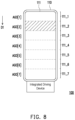
- FIG. 8 is a schematic diagram showing sensing zones of a sensing pixel array of a touch display panel according to an embodiment of the disclosure.
- the sensing pixel array 111 is divided into seven sensing zones 111 _ 1 to 111 _ 7 along a scanning direction D1 such as from up to down.
- Each sensing zone includes a plurality of fingerprint sensing pixel rows.
- AGO[ 1 ] to AGO[ 7 ] represent control signals provided from the optical sensing circuit 121 to the GOA circuit on the touch display panel, corresponding to the sensing zones, and each control signal among AGO[ 1 ] to AGO[ 7 ] is configured to reset or readout all the fingerprint sensing pixel rows of a respective sensing zone at the same time.
- only one of the sensing zones e.g., the sensing zone 111 _ 2 , is configured for ambient light detection.
- all fingerprint sensing pixel rows in the sensing zone 111 _ 2 are turned on (i.e., reset and readout) at the same time during the fingerprint sensing period.
- reset operation is performed on the fingerprint sensing pixel rows of the sensing zone 111 _ 2 at the same time, and then readout operation on the fingerprint sensing pixel rows of the sensing zone 111 _ 2 is performed thereon at the same time.
- the ambient light sensing signal read back through a sensing line is the summed result of the ambient light sensing signals of the multiple fingerprint sensing pixel rows.
- Ambient light information may be obtained through average brightness calculation on the ambient light sensing signals read back.
- FIG. 9 A is a timing diagram of ambient light sensing of a plurality of sensing zones of a sensing pixel array according to the embodiment of FIG. 8 of the disclosure.
- STV[ 1 ] to STV[ 7 ] in FIG. 9 A respectively represent start pulse signals provided by the optical sensing circuit 121 to the GOA circuit, corresponding to the first sensing zone 111 _ 1 to the seventh sensing zone 111 _ 7 .
- Each control signal among control signals AGOR[ 1 ] to AGOR[ 7 ] is configured to reset all the fingerprint sensing pixel rows of a respective sensing zone at the same time, and each control signal among control signals AGOS[ 1 ] to AGOS[ 7 ] is configured to readout all the fingerprint sensing pixel rows of the respective sensing zone at the same time, which means different optical sensing signals from different fingerprint sensing pixel rows may be readout through a sensing line at the same time instead of being sequentially readout.
- Rest[ 1 ] to Rest[Y] represent reset signals generated by the GOA circuit and provided to the Y fingerprint sensing pixel rows of the sensing zone 111 _ 2 .
- Sel[ 1 ] to Sel[Y] represent select signals generated by the GOA circuit and provided to the Y fingerprint sensing pixel rows of the sensing zone 111 _ 2 . Since only the sensing zone 111 _ 2 is used for ambient light sensing, only the start pulse signal STV[ 2 ] has active start pulses and only the control signal AGOR[ 2 ] and the control signal AGOS[ 2 ] have active pulses. The start pulse signals STV[ 1 ] and STV[ 3 ] to STV[ 7 ] do not have active pulses. The control signals AGOR[ 1 ] and AGOR[ 3 ] to AGOR[ 7 ], the control signals AGOS[ 1 ] and AGOS[ 3 ] to AGOS[ 7 ] do not have active pulses.
- Vout represents an output voltage (i.e., sensing signal) obtained from a sensing line.
- multiple frame periods from a frame period F_N to a frame period F_N+k
- two frame periods are required means that the end of the exposure period falls within the second frame period, and does not means that the exposure period fully takes two frame periods.
- fingerprint sensing pixel rows in any number and in any position may be set to be turned on (i.e. reset, and readout) at the same time.
- the fingerprint sensing pixel rows of the second sensing zone 111 _ 2 and the fifth sensing zone 111 _ 5 may be turned on at the same time.
- the fingerprint sensing pixel rows of the second sensing zone 111 _ 2 , the fourth sensing zone 111 _ 4 , and the sixth sensing zone 111 _ 6 may be turned on at the same time.
- the number of ambient light sensing periods LS during one frame period for ambient light sensing is not limited. However, at least one ambient light sensing period LS is required.
- FIG. 9 B is a timing diagram of ambient light sensing of a plurality of sensing zones of a sensing pixel array according to an embodiment of the disclosure.
- FIG. 9 B is similarly further to describe the embodiment shown in FIG. 8 .
- the difference between the two only lies in that, in FIG. 9 B , the exposure is completed within one frame period.
- the fingerprint sensor of the second sensing zone 111 _ 2 requires a short exposure period TE such that an ambient light sensing cycle may be completed in only one frame period F_N.
- FIG. 10 is a schematic block diagram showing a GOA circuit according to an embodiment of the disclosure.
- the touch display panel 110 is provided with the sensing pixel array 111 and a GOA circuit.
- a GOA circuit 112 disposed at the left side of the sensing pixel array 111 represents one of a plurality of similar circuits, for generating reset signals with respect to one sensing zone.
- the GOA circuit 112 includes a plurality of shift register circuits.
- the GOA circuit 112 outputs a plurality of reset signals, including SR[n ⁇ 1], SR[n], SR[n+1] and so on, to sensing pixel rows of the second sensing zone 111 _ 2 of FIG. 10 according to a start pulse signal STV[ 2 ], a reset control signal AGOR[ 2 ], a first shift direction control signal U2D which enables a direction from up to down and a second shift direction control signal D2U which enables a direction from down to up.
- the two shift direction control signals are provided by the optical sensing circuit 121 and are configured to control the shift register circuits of the GOA circuit 112 to sequentially output active pulses either downward or upward.
- the reset signals SR[n ⁇ 1], SR[n], SR[n+1] and all other reset signals with respect to the sensing zone 111 _ 2 are pulled high (active) at the same time by the reset control signal AGOR[ 2 ] such that the timing of reset operation like FIG. 9 A or FIG. 9 B can be realized.
- a reset signal Rest may be used for resetting the GOA circuit 112 with respect to the second sensing zone 111 _ 2 .
- FIG. 11 A and FIG. 11 B are each a schematic diagram showing a relationship of a plurality of light sensing cycles and corresponding sensing zones according to an embodiment of the disclosure.
- a sensing pixel array may be divided into a plurality of sensing zones by a horizontal direction and a vertical direction.
- Scan1 to ScanN denotes a plurality of light sensing cycles (or said scanning cycles) performed in an order, and each of Scan1 to ScanN are respectively remarked in the position of a corresponding sensing zone.
- FIG. 11 A and FIG. 11 B are each a schematic diagram showing a relationship of a plurality of light sensing cycles and corresponding sensing zones according to an embodiment of the disclosure.
- a sensing pixel array may be divided into a plurality of sensing zones by a horizontal direction and a vertical direction.
- Scan1 to ScanN denotes a plurality of light sensing cycles (or said scanning cycles) performed in an order, and each of Scan1 to ScanN are respectively
- the optical sensing circuit 121 may start a first light sensing cycle SCAN1 for generating first ambient light information in a first frame period, and start a second optical sensing cycle SCAN2 for generating second ambient light information in a second frame period (different from the first frame period), and so on. Because the sensing pixel array are divided not only along the vertical direction but also the horizontal direction, the optical sensing circuit 121 may receive sensing signals from different group of sensing lines for different ambient light sensing cycle. In the example of FIG. 11 A , sensing zones are used from left to right and from top to bottom. The sensing zones may be fully different or partially different.
- FIG. 11 B illustrates that the position of a sensing zone used in each ambient light sensing cycle changes in a different way.
- Rows of sensing zones are used interlacedly from top to bottom, which means odd rows of sensing zones are used sequentially from top to bottom and then even rows of sensing zones are used sequentially from top to bottom, and with respect to each row (no matter odd or even) of sensing zones, the position of a sensing zone used in each ambient light sensing cycle changes from left to right.
- the position of a sensing zone used in each respective light sensing cycle may be changed in an order or randomly.
- FIG. 12 A and FIG. 12 B are each a schematic diagram showing a relationship of a plurality of light sensing cycles and corresponding sensing zones according to an embodiment of the disclosure.
- three sensing zones in the horizontal direction is used in each light sensing cycle.
- Scan1 to ScanN denotes a plurality of light sensing cycles (or said scanning cycles) performed in an order and each of Scan1 to ScanN are respectively remarked in the position of a corresponding sensing zone.
- the position of a sensing zone used in each ambient light sensing cycle changes from top to bottom.
- the position of a sensing zone used in each ambient light sensing cycle changes interlacedly from top to bottom, which means odd sensing zones are used sequentially from top to bottom then even sensing zones are used sequentially from top to bottom.
- the position of a sensing zone used in each respective light sensing cycle may be changed in an order or randomly.
- FIG. 13 is a schematic diagram showing ambient light sensing of a plurality of zones of a sensing pixel array according to an embodiment of the disclosure.
- each of the sensing zones 111 _ 1 to 111 _ 7 includes Y fingerprint sensing pixel rows (Y is a positive integer), and a part of the fingerprint sensing pixel rows in each of the sensing zones serve for ambient light sensing.
- Y is a positive integer
- only the 1 st to 3 rd rows of the fingerprint sensing pixel rows in each sensing zone serve for ambient light sensing, and may be designed to be turned on in sequence or at the same time.
- the sensing signal obtained during one readout period may include the summed sensing result of multiple fingerprint sensing pixel rows.
- the optical sensing circuit 121 may perform average brightness calculation on the sensing signals read back to obtain ambient light information.
- FIG. 14 A is a timing diagram of ambient light sensing according to an embodiment of the disclosure.
- FIG. 14 A is further to describe the embodiment shown in FIG. 13 , in which, through the start pulse signals STV[ 1 ] to STV[ 7 ] where each start pulse signal has active pulses, the first row of the fingerprint sensing pixel rows of each sensing zone is turned on at the same time.
- the reset signals Rest[ 1 ] to Rest[ 3 ] have active pulses such that the 1 st to 3 rd fingerprint sensing pixel rows of each sensing zone are reset sequentially.
- the reset signals Rest[ 4 ] to Rest[Y] do not have active pulses.
- the select signals Sel[ 1 ] to Sel[ 3 ] have active pulses such that the 1 st to 3 rd fingerprint sensing pixel rows of each sensing zone are readout sequentially.
- the select signals Sel[ 4 ] to Sel[Y] do not have active pulses.
- the exposure period required for ambient light sensing is long such that the readout operation cannot be completed within the same fame period where the reset operation is performed.
- FIG. 14 B is a timing diagram of ambient light sensing according to an embodiment of the disclosure. FIG. 14 B is also further to describe the embodiment shown in FIG. 13 . Compared with FIG. 14 A , in FIG. 14 B , the exposure period required for ambient light sensing is short such that reset operation and the readout operation of an ambient light sensing cycle are completed in a frame period F1.
- FIG. 15 is a schematic waveform diagram of performing “fast skip” according to an embodiment of the disclosure.
- STV[X] is pulled up
- scanning is performed on the sensing pixel rows.
- X is a positive integer and 1 ⁇ X ⁇ 7.
- the width of each pulse of a clock signal CLK in scanning intervals SC1 and SC3 is reduced, such that the unused sensing pixel rows may be quickly scanned.
- each pulse of the clock signal CLK in a scanning interval SC2 remains normal, such that the used sensing pixel rows may be scanned normally.
- the fingerprint sensing pixel rows scanned in the same sensing zone may be made different (or not completely the same) each time, in case that long-term and fixed-position detection results in excessive difference in performance degradation between the fingerprint sensing pixels therein and other regions.
- FIG. 16 is a flowchart of an operation method of an integrated driving device according to an embodiment of the disclosure.
- the integrated driving device includes at least the optical sensing circuit 121 and the touch sensing circuit 1221 .
- touch sensing is performed by the touch sensing circuit 1221 in a plurality of touch sensing periods during a first frame period.
- optical sensing is performed by the optical sensing circuit 121 during at least one optical sensing period during the first frame period to obtain optical sensing signals for generating first ambient light information.
- the touch sensing periods and the optical sensing period are non-overlapping.
- the blocks of the application processor 130 , the optical sensing circuit 121 , the touch sensing circuit 1221 , and the display driving circuit 1222 may be logic circuits implemented on an integrated circuit. Relevant functions of the application processor 130 , the optical sensing circuit 121 , the touch sensing circuit 1221 , and the display driving circuit 1222 may be implemented in a hardware form by utilizing hardware description languages (e.g., Verilog HDL or VHDL) or other appropriate programming languages.
- hardware description languages e.g., Verilog HDL or VHDL
- the relevant functions of the application processor 130 , the optical sensing circuit 121 , the touch sensing circuit 1221 , and the display driving circuit 1222 may be implemented in one or more controllers, microcontrollers, microprocessors, application-specific integrated circuits, (ASIC), digital signal processors (DSP), field programmable gate arrays (FPGA) and/or various logic blocks, modules, and circuits in other processing units.
- ASIC application-specific integrated circuits
- DSP digital signal processors
- FPGA field programmable gate arrays
- the relevant functions of the application processor 130 , the optical sensing circuit 121 , the touch sensing circuit 1221 , and the display driving circuit 1222 may be implemented as programming codes.
- the application processor 130 , the optical sensing circuit 121 , the touch sensing circuit 1221 , and the display driving circuit 1222 may be implemented by utilizing general programming languages (e.g., C, C++, or assembly language) or other appropriate programming languages.
- the programming codes may be recorded/stored in a recording medium, and the recording medium includes, for example, a read only memory (ROM), a storage device, and/or a random access memory (RAM).
- a computer, central processing unit (CPU), controller, microcontroller, or microprocessor may read and execute the programming codes from the recording medium to achieve the relevant functions.
- a “non-transitory computer readable medium”, such as a tape, disk, card, semiconductor memory, programmable logic circuit, etc., may serve as the recording medium.
- the programs may also be provided to the computer (or CPU) through any transmission medium (communication network, broadcast radio wave, or the like).
- the communication network is, for example, the Internet, wired communication, wireless communication, or other communication media.
- the in-display fingerprint sensor of the disclosure may be configured to perform not only fingerprint sensing but also ambient light sensing (collectively referred to as optical sensing).
- the backlight brightness of the screen of the handheld electronic device may be dynamically adjusted according to the sensed ambient light information.
- the length of the exposure period of the subsequent fingerprint recognition may be dynamically adjusted according to the sensed ambient light information. In this way, an standalone ambient light sensor in the handheld electronic device is not required, and various applications may be executed based on the sensed ambient light information.
Abstract
Description
Claims (50)
Priority Applications (1)
| Application Number | Priority Date | Filing Date | Title |
|---|---|---|---|
| US17/241,091 US11922844B2 (en) | 2020-04-27 | 2021-04-27 | Integrated driving device and operation method thereof |
Applications Claiming Priority (2)
| Application Number | Priority Date | Filing Date | Title |
|---|---|---|---|
| US202063015698P | 2020-04-27 | 2020-04-27 | |
| US17/241,091 US11922844B2 (en) | 2020-04-27 | 2021-04-27 | Integrated driving device and operation method thereof |
Publications (2)
| Publication Number | Publication Date |
|---|---|
| US20220171494A1 US20220171494A1 (en) | 2022-06-02 |
| US11922844B2 true US11922844B2 (en) | 2024-03-05 |
Family
ID=78415760
Family Applications (1)
| Application Number | Title | Priority Date | Filing Date |
|---|---|---|---|
| US17/241,091 Active 2041-07-02 US11922844B2 (en) | 2020-04-27 | 2021-04-27 | Integrated driving device and operation method thereof |
Country Status (3)
| Country | Link |
|---|---|
| US (1) | US11922844B2 (en) |
| CN (1) | CN113642375A (en) |
| TW (1) | TWI800822B (en) |
Families Citing this family (6)
| Publication number | Priority date | Publication date | Assignee | Title |
|---|---|---|---|---|
| CN113642375A (en) * | 2020-04-27 | 2021-11-12 | 联咏科技股份有限公司 | Integrated driving device and operation method thereof |
| WO2022051954A1 (en) * | 2020-09-10 | 2022-03-17 | 京东方科技集团股份有限公司 | Fingerprint detection control circuit, fingerprint detection control method, and display device |
| US11640802B2 (en) * | 2021-05-20 | 2023-05-02 | E Ink Holdings Inc. | Display device and display device driving method |
| TWI771028B (en) * | 2021-05-31 | 2022-07-11 | 友達光電股份有限公司 | Display panel and emission control circuit thereof |
| CN113899449A (en) * | 2021-09-30 | 2022-01-07 | 深圳市汇顶科技股份有限公司 | Method for detecting ambient light sensing value, electronic device and storage medium |
| CN114581964A (en) * | 2022-02-22 | 2022-06-03 | 业泓科技(成都)有限公司 | Screen lower fingerprint identification circuit and laminated structure thereof, display panel and fingerprint acquisition method |
Citations (32)
| Publication number | Priority date | Publication date | Assignee | Title |
|---|---|---|---|---|
| US4818856A (en) * | 1985-11-06 | 1989-04-04 | Nippondenso Co., Ltd. | Optical information reading apparatus |
| US20060066876A1 (en) | 2004-09-27 | 2006-03-30 | Manish Kothari | Method and system for sensing light using interferometric elements |
| US7391408B1 (en) * | 2007-03-27 | 2008-06-24 | Lite-On Semiconductor Corp. | Adjustable apparatus in display devices for automatic adjusting brightness |
| US20120313913A1 (en) * | 2010-02-26 | 2012-12-13 | Sharp Kabushiki Kaisha | Display device |
| US20180173923A1 (en) * | 2016-12-16 | 2018-06-21 | Lg Display Co., Ltd. | Display device, display panel, fingerprint-sensing method, and circuit for sensing fingerprint |
| CN108229372A (en) | 2017-12-29 | 2018-06-29 | 努比亚技术有限公司 | Fingerprint identification method, mobile terminal and computer readable storage medium |
| US20180259321A1 (en) | 2017-03-07 | 2018-09-13 | Guangdong Oppo Mobile Telecommunications Corp., Ltd. | Functional assembly, display device and terminal |
| US20180306640A1 (en) | 2017-04-19 | 2018-10-25 | Shenzhen GOODIX Technology Co., Ltd. | Light intensity detection method and apparatus, and intelligent terminal |
| US20190095671A1 (en) * | 2017-09-28 | 2019-03-28 | Apple Inc. | Electronic device including sequential operation of light source subsets while acquiring biometric image data and related methods |
| US20190180075A1 (en) * | 2017-12-12 | 2019-06-13 | Silicon Display Technology | Sensor pixel, fingerprint and image sensor including the same, and driving method thereof |
| US20200134285A1 (en) * | 2016-12-13 | 2020-04-30 | Novatek Microelectronics Corp. | Touch apparatus and touch detection integrated circuit thereof |
| US20200183563A1 (en) * | 2018-12-06 | 2020-06-11 | Hon Hai Precision Industry Co., Ltd. | Touch display panel and method for driving touch display panel |
| US20200210065A1 (en) * | 2018-12-27 | 2020-07-02 | Novatek Microelectronics Corp. | Electronic device and fingerprint sensing control method thereof |
| US20200250288A1 (en) * | 2017-04-21 | 2020-08-06 | Shenzhen GOODIX Technology Co., Ltd. | Biological data detection method, biological data detection device |
| US20200320956A1 (en) * | 2019-04-02 | 2020-10-08 | Beijing Boe Display Technology Co., Ltd. | Display panel, driving method and manufacturing method thereof, and display device |
| US20200327301A1 (en) * | 2019-04-09 | 2020-10-15 | Novatek Microelectronics Corp. | Driving apparatus and operation method thereof |
| US11030435B1 (en) * | 2020-03-24 | 2021-06-08 | Novatek Microelectronics Corp. | Image sensing method and system |
| US20210191545A1 (en) * | 2019-12-20 | 2021-06-24 | Xiamen Tianma Micro-Electronics Co.,Ltd | Display panel and display device |
| US20210192168A1 (en) * | 2019-12-03 | 2021-06-24 | Novatek Microelectronics Corp. | Fingerprint sensing control device and operation method thereof |
| US20210224548A1 (en) * | 2020-01-22 | 2021-07-22 | Novatek Microelectronics Corp. | Driving device and operation method thereof |
| US20210266483A1 (en) * | 2020-02-26 | 2021-08-26 | Beijing Xiaomi Mobile Software Co., Ltd. | Light sensor module, method for acquiring light sensor data, and electronic equipment |
| US11113496B1 (en) * | 2020-05-06 | 2021-09-07 | Wuhan China Star Optoelectronics Technology Co., Ltd. | Fingerprint recognition driving circuit |
| US20210303815A1 (en) * | 2020-03-25 | 2021-09-30 | Novatek Microelectronics Corp. | System, device, method related to fingerprint sensing |
| US20210326561A1 (en) * | 2020-04-08 | 2021-10-21 | Shenzhen GOODIX Technology Co., Ltd. | Fingerprint identification method, fingerprint identification apparatus and electronic device |
| US20210365660A1 (en) * | 2020-05-21 | 2021-11-25 | Novatek Microelectronics Corp. | Optical fingerprint sensing device and optical fingerprint sensing method |
| US11200399B1 (en) * | 2020-09-28 | 2021-12-14 | Xiamen Tianma Micro-Electronics Co., Ltd. | Display panel and driving method of display panel |
| US20220012454A1 (en) * | 2020-07-07 | 2022-01-13 | Novatek Microelectronics Corp. | Fingerprint recognition driving method for display panel |
| US20220050993A1 (en) * | 2020-08-13 | 2022-02-17 | Novatek Microelectronics Corp. | Optical fingerprint sensing apparatus, driver apparatus thereof and operation method |
| US20220050984A1 (en) * | 2020-08-14 | 2022-02-17 | Samsung Display Co., Ltd. | Input sensing method and input sensing device including the same |
| US20220058368A1 (en) * | 2020-08-18 | 2022-02-24 | Innolux Corporation | Fingerprint Identification Method by Using Electronic Device and the Electronic Device Thereof |
| US20220092287A1 (en) * | 2020-09-21 | 2022-03-24 | Novatek Microelectronics Corp. | Electronic circuit and a gate driver circuit |
| US20220171494A1 (en) * | 2020-04-27 | 2022-06-02 | Novatek Microelectronics Corp. | Integrated driving device and operation method thereof |
-
2021
- 2021-04-27 CN CN202110460230.6A patent/CN113642375A/en active Pending
- 2021-04-27 US US17/241,091 patent/US11922844B2/en active Active
- 2021-04-27 TW TW110115167A patent/TWI800822B/en active
Patent Citations (48)
| Publication number | Priority date | Publication date | Assignee | Title |
|---|---|---|---|---|
| US4818856A (en) * | 1985-11-06 | 1989-04-04 | Nippondenso Co., Ltd. | Optical information reading apparatus |
| US20060066876A1 (en) | 2004-09-27 | 2006-03-30 | Manish Kothari | Method and system for sensing light using interferometric elements |
| TW200624781A (en) | 2004-09-27 | 2006-07-16 | Idc Llc | Method and system for sensing light using interferometric elements |
| US7460246B2 (en) | 2004-09-27 | 2008-12-02 | Idc, Llc | Method and system for sensing light using interferometric elements |
| US20090141286A1 (en) | 2004-09-27 | 2009-06-04 | Idc, Llc | Method and system for sensing light using interferometric elements |
| US7852483B2 (en) | 2004-09-27 | 2010-12-14 | Qualcomm Mems Technologies, Inc. | Method and system for sensing light using an interferometric element having a coupled temperature sensor |
| US7391408B1 (en) * | 2007-03-27 | 2008-06-24 | Lite-On Semiconductor Corp. | Adjustable apparatus in display devices for automatic adjusting brightness |
| US20120313913A1 (en) * | 2010-02-26 | 2012-12-13 | Sharp Kabushiki Kaisha | Display device |
| US11036952B2 (en) * | 2016-12-13 | 2021-06-15 | Novatek Microelectronics Corp. | Touch apparatus and touch detection integrated circuit thereof |
| US20200134285A1 (en) * | 2016-12-13 | 2020-04-30 | Novatek Microelectronics Corp. | Touch apparatus and touch detection integrated circuit thereof |
| US20180173923A1 (en) * | 2016-12-16 | 2018-06-21 | Lg Display Co., Ltd. | Display device, display panel, fingerprint-sensing method, and circuit for sensing fingerprint |
| US20180259321A1 (en) | 2017-03-07 | 2018-09-13 | Guangdong Oppo Mobile Telecommunications Corp., Ltd. | Functional assembly, display device and terminal |
| TW201833607A (en) | 2017-03-07 | 2018-09-16 | 廣東歐珀移動通信有限公司 | Functional components, display devices and terminals |
| US10508901B2 (en) | 2017-03-07 | 2019-12-17 | Guangdong Oppo Mobile Telecommunications Corp., Ltd. | Functional assembly, display device and terminal |
| US20190094014A1 (en) | 2017-03-07 | 2019-03-28 | Guangdong Oppo Mobile Telecommunications Corp., Ltd. | Functional assembly, display device and terminal |
| US10724851B2 (en) | 2017-03-07 | 2020-07-28 | Guangdong Oppo Mobile Telecommunications Corp., Ltd. | Functional assembly, display device and terminal |
| US20180306640A1 (en) | 2017-04-19 | 2018-10-25 | Shenzhen GOODIX Technology Co., Ltd. | Light intensity detection method and apparatus, and intelligent terminal |
| US20200250288A1 (en) * | 2017-04-21 | 2020-08-06 | Shenzhen GOODIX Technology Co., Ltd. | Biological data detection method, biological data detection device |
| US20190095671A1 (en) * | 2017-09-28 | 2019-03-28 | Apple Inc. | Electronic device including sequential operation of light source subsets while acquiring biometric image data and related methods |
| US20190180075A1 (en) * | 2017-12-12 | 2019-06-13 | Silicon Display Technology | Sensor pixel, fingerprint and image sensor including the same, and driving method thereof |
| US10755070B2 (en) * | 2017-12-12 | 2020-08-25 | Silicon Display Technology | Sensor pixel, fingerprint and image sensor including the same, and driving method thereof |
| CN108229372A (en) | 2017-12-29 | 2018-06-29 | 努比亚技术有限公司 | Fingerprint identification method, mobile terminal and computer readable storage medium |
| US20200183563A1 (en) * | 2018-12-06 | 2020-06-11 | Hon Hai Precision Industry Co., Ltd. | Touch display panel and method for driving touch display panel |
| US10761653B2 (en) * | 2018-12-06 | 2020-09-01 | Hon Hai Precision Industry Co., Ltd. | Touch display panel and method for driving touch display panel |
| US20200210065A1 (en) * | 2018-12-27 | 2020-07-02 | Novatek Microelectronics Corp. | Electronic device and fingerprint sensing control method thereof |
| US11093080B2 (en) * | 2018-12-27 | 2021-08-17 | Novatek Microelectronics Corp. | Electronic device and fingerprint sensing control method thereof |
| US20200320956A1 (en) * | 2019-04-02 | 2020-10-08 | Beijing Boe Display Technology Co., Ltd. | Display panel, driving method and manufacturing method thereof, and display device |
| US10916219B2 (en) * | 2019-04-02 | 2021-02-09 | Beijing Boe Display Technology Co., Ltd. & Boe Technology Group Co., Ltd. | Display panel, driving method and manufacturing method thereof, and display device |
| US20200327301A1 (en) * | 2019-04-09 | 2020-10-15 | Novatek Microelectronics Corp. | Driving apparatus and operation method thereof |
| US11244137B2 (en) * | 2019-12-03 | 2022-02-08 | Novatek Microelectronics Corp. | Fingerprint sensing control device and operation method thereof |
| US20210192168A1 (en) * | 2019-12-03 | 2021-06-24 | Novatek Microelectronics Corp. | Fingerprint sensing control device and operation method thereof |
| US20210191545A1 (en) * | 2019-12-20 | 2021-06-24 | Xiamen Tianma Micro-Electronics Co.,Ltd | Display panel and display device |
| US20210224548A1 (en) * | 2020-01-22 | 2021-07-22 | Novatek Microelectronics Corp. | Driving device and operation method thereof |
| US20210224505A1 (en) * | 2020-01-22 | 2021-07-22 | Novatek Microelectronics Corp. | Method for controlling display panel and control circuit using the same |
| US11302102B2 (en) * | 2020-01-22 | 2022-04-12 | Novatek Microelectronics Corp. | Method for controlling display panel and control circuit using the same |
| US20210266483A1 (en) * | 2020-02-26 | 2021-08-26 | Beijing Xiaomi Mobile Software Co., Ltd. | Light sensor module, method for acquiring light sensor data, and electronic equipment |
| US11030435B1 (en) * | 2020-03-24 | 2021-06-08 | Novatek Microelectronics Corp. | Image sensing method and system |
| US20210303815A1 (en) * | 2020-03-25 | 2021-09-30 | Novatek Microelectronics Corp. | System, device, method related to fingerprint sensing |
| US20210326561A1 (en) * | 2020-04-08 | 2021-10-21 | Shenzhen GOODIX Technology Co., Ltd. | Fingerprint identification method, fingerprint identification apparatus and electronic device |
| US20220171494A1 (en) * | 2020-04-27 | 2022-06-02 | Novatek Microelectronics Corp. | Integrated driving device and operation method thereof |
| US11113496B1 (en) * | 2020-05-06 | 2021-09-07 | Wuhan China Star Optoelectronics Technology Co., Ltd. | Fingerprint recognition driving circuit |
| US20210365660A1 (en) * | 2020-05-21 | 2021-11-25 | Novatek Microelectronics Corp. | Optical fingerprint sensing device and optical fingerprint sensing method |
| US20220012454A1 (en) * | 2020-07-07 | 2022-01-13 | Novatek Microelectronics Corp. | Fingerprint recognition driving method for display panel |
| US20220050993A1 (en) * | 2020-08-13 | 2022-02-17 | Novatek Microelectronics Corp. | Optical fingerprint sensing apparatus, driver apparatus thereof and operation method |
| US20220050984A1 (en) * | 2020-08-14 | 2022-02-17 | Samsung Display Co., Ltd. | Input sensing method and input sensing device including the same |
| US20220058368A1 (en) * | 2020-08-18 | 2022-02-24 | Innolux Corporation | Fingerprint Identification Method by Using Electronic Device and the Electronic Device Thereof |
| US20220092287A1 (en) * | 2020-09-21 | 2022-03-24 | Novatek Microelectronics Corp. | Electronic circuit and a gate driver circuit |
| US11200399B1 (en) * | 2020-09-28 | 2021-12-14 | Xiamen Tianma Micro-Electronics Co., Ltd. | Display panel and driving method of display panel |
Non-Patent Citations (1)
| Title |
|---|
| "Office Action of Taiwan Counterpart Application", dated Mar. 10, 2022, p. 1-p. 4. |
Also Published As
| Publication number | Publication date |
|---|---|
| TW202141005A (en) | 2021-11-01 |
| CN113642375A (en) | 2021-11-12 |
| TWI800822B (en) | 2023-05-01 |
| US20220171494A1 (en) | 2022-06-02 |
Similar Documents
| Publication | Publication Date | Title |
|---|---|---|
| US11922844B2 (en) | Integrated driving device and operation method thereof | |
| CN107967888B (en) | Gate drive circuit, drive method thereof and display panel | |
| US8144134B2 (en) | Sensing circuit, display device, and electronic apparatus | |
| US20220406085A1 (en) | Driving apparatus and operation method thereof | |
| CN104182080A (en) | Semiconductor device and display device | |
| US11462044B2 (en) | Electronic device, chip, panel, decoder and operation method thereof | |
| US10629117B2 (en) | Detection circuit, pixel electrical signal collection circuit, display panel and display apparatus | |
| US10345937B2 (en) | Electronic device with a backlight and capacitive touch panel and method for controlling electronic device so as to suppress error detection of a touch operation | |
| US11244137B2 (en) | Fingerprint sensing control device and operation method thereof | |
| TWI789816B (en) | Fingerprint recognition driving method for display panel | |
| US20200275001A1 (en) | Display apparatus and fingerprint sensing method thereof | |
| CN111126343B (en) | Driving method and driving device for photoelectric sensor and display device | |
| US11442575B2 (en) | Touch display driving apparatus and operation method thereof | |
| US11715322B2 (en) | Fingerprint sensing apparatus, fingerprint readout circuit, and touch display panel | |
| US11615640B2 (en) | Driving device and operation method thereof | |
| CN114637423A (en) | Display panel, driving method thereof and display device | |
| US20210333974A1 (en) | Touch detection method and touch display device | |
| CN110334700B (en) | Fingerprint sensing module | |
| US10402013B2 (en) | Level converter and operation method thereof, gate driving circuit and display device | |
| KR20170100388A (en) | Touch display driving integrated circuit, operation method of the same, and touch display device including the same | |
| JP6532582B2 (en) | Liquid crystal monitor, electronic device, control method, and program | |
| CN114170942B (en) | Display panel, driving method thereof and display device | |
| US11709565B2 (en) | Fingerprint sensing apparatus, fingerprint readout circuit, and touch display panel | |
| CN112883903B (en) | Display panel driving method and display device | |
| CN116543683A (en) | Display module, display device and control method of display module |
Legal Events
| Date | Code | Title | Description |
|---|---|---|---|
| AS | Assignment |
Owner name: NOVATEK MICROELECTRONICS CORP., TAIWAN Free format text: ASSIGNMENT OF ASSIGNORS INTEREST;ASSIGNORS:SHIH, WEI-LUN;LIN, WU-WEI;TSAI, JIUN-JIE;AND OTHERS;REEL/FRAME:056045/0953 Effective date: 20210413 |
|
| FEPP | Fee payment procedure |
Free format text: ENTITY STATUS SET TO UNDISCOUNTED (ORIGINAL EVENT CODE: BIG.); ENTITY STATUS OF PATENT OWNER: LARGE ENTITY |
|
| STPP | Information on status: patent application and granting procedure in general |
Free format text: DOCKETED NEW CASE - READY FOR EXAMINATION |
|
| STPP | Information on status: patent application and granting procedure in general |
Free format text: NON FINAL ACTION MAILED |
|
| STPP | Information on status: patent application and granting procedure in general |
Free format text: FINAL REJECTION MAILED |
|
| STPP | Information on status: patent application and granting procedure in general |
Free format text: RESPONSE TO NON-FINAL OFFICE ACTION ENTERED AND FORWARDED TO EXAMINER |
|
| STPP | Information on status: patent application and granting procedure in general |
Free format text: FINAL REJECTION MAILED |
|
| STPP | Information on status: patent application and granting procedure in general |
Free format text: DOCKETED NEW CASE - READY FOR EXAMINATION |
|
| STPP | Information on status: patent application and granting procedure in general |
Free format text: NOTICE OF ALLOWANCE MAILED -- APPLICATION RECEIVED IN OFFICE OF PUBLICATIONS |
|
| STPP | Information on status: patent application and granting procedure in general |
Free format text: PUBLICATIONS -- ISSUE FEE PAYMENT VERIFIED |
|
| STCF | Information on status: patent grant |
Free format text: PATENTED CASE |