US11901193B2 - Fabrication method of device with cavity - Google Patents
Fabrication method of device with cavity Download PDFInfo
- Publication number
- US11901193B2 US11901193B2 US18/315,091 US202318315091A US11901193B2 US 11901193 B2 US11901193 B2 US 11901193B2 US 202318315091 A US202318315091 A US 202318315091A US 11901193 B2 US11901193 B2 US 11901193B2
- Authority
- US
- United States
- Prior art keywords
- dielectric layer
- substrate
- layer
- etching
- cavity
- Prior art date
- Legal status (The legal status is an assumption and is not a legal conclusion. Google has not performed a legal analysis and makes no representation as to the accuracy of the status listed.)
- Active
Links
- 238000000034 method Methods 0.000 title claims abstract description 67
- 238000004519 manufacturing process Methods 0.000 title description 3
- 239000000758 substrate Substances 0.000 claims abstract description 72
- 238000005530 etching Methods 0.000 claims abstract description 29
- 238000000151 deposition Methods 0.000 claims abstract description 12
- 238000004381 surface treatment Methods 0.000 claims abstract description 11
- 239000010410 layer Substances 0.000 claims description 149
- 239000000463 material Substances 0.000 claims description 15
- XUIMIQQOPSSXEZ-UHFFFAOYSA-N Silicon Chemical compound [Si] XUIMIQQOPSSXEZ-UHFFFAOYSA-N 0.000 claims description 10
- 229910052710 silicon Inorganic materials 0.000 claims description 10
- 239000010703 silicon Substances 0.000 claims description 10
- 229910052581 Si3N4 Inorganic materials 0.000 claims description 9
- HQVNEWCFYHHQES-UHFFFAOYSA-N silicon nitride Chemical compound N12[Si]34N5[Si]62N3[Si]51N64 HQVNEWCFYHHQES-UHFFFAOYSA-N 0.000 claims description 9
- VYPSYNLAJGMNEJ-UHFFFAOYSA-N Silicium dioxide Chemical compound O=[Si]=O VYPSYNLAJGMNEJ-UHFFFAOYSA-N 0.000 claims description 8
- PMHQVHHXPFUNSP-UHFFFAOYSA-M copper(1+);methylsulfanylmethane;bromide Chemical compound Br[Cu].CSC PMHQVHHXPFUNSP-UHFFFAOYSA-M 0.000 claims description 7
- 229910052814 silicon oxide Inorganic materials 0.000 claims description 7
- 238000005498 polishing Methods 0.000 claims description 6
- 230000001133 acceleration Effects 0.000 claims description 5
- 239000004065 semiconductor Substances 0.000 claims description 5
- 239000000126 substance Substances 0.000 claims description 5
- 238000010884 ion-beam technique Methods 0.000 claims description 4
- 238000001020 plasma etching Methods 0.000 claims description 4
- 239000002344 surface layer Substances 0.000 claims description 4
- 229910002601 GaN Inorganic materials 0.000 claims description 2
- JMASRVWKEDWRBT-UHFFFAOYSA-N Gallium nitride Chemical compound [Ga]#N JMASRVWKEDWRBT-UHFFFAOYSA-N 0.000 claims description 2
- 229910021417 amorphous silicon Inorganic materials 0.000 claims description 2
- 229910021420 polycrystalline silicon Inorganic materials 0.000 claims description 2
- 229920005591 polysilicon Polymers 0.000 claims description 2
- 229910021421 monocrystalline silicon Inorganic materials 0.000 claims 1
- 229920002120 photoresistant polymer Polymers 0.000 description 7
- 238000000206 photolithography Methods 0.000 description 3
- 230000000052 comparative effect Effects 0.000 description 2
- 230000003213 activating effect Effects 0.000 description 1
- 238000004140 cleaning Methods 0.000 description 1
- 238000007796 conventional method Methods 0.000 description 1
- 238000007517 polishing process Methods 0.000 description 1
- 239000011241 protective layer Substances 0.000 description 1
- 239000002210 silicon-based material Substances 0.000 description 1
- 239000002904 solvent Substances 0.000 description 1
- 230000003313 weakening effect Effects 0.000 description 1
Images


Classifications
-
- H—ELECTRICITY
- H01—ELECTRIC ELEMENTS
- H01L—SEMICONDUCTOR DEVICES NOT COVERED BY CLASS H10
- H01L21/00—Processes or apparatus adapted for the manufacture or treatment of semiconductor or solid state devices or of parts thereof
- H01L21/02—Manufacture or treatment of semiconductor devices or of parts thereof
- H01L21/04—Manufacture or treatment of semiconductor devices or of parts thereof the devices having at least one potential-jump barrier or surface barrier, e.g. PN junction, depletion layer or carrier concentration layer
- H01L21/18—Manufacture or treatment of semiconductor devices or of parts thereof the devices having at least one potential-jump barrier or surface barrier, e.g. PN junction, depletion layer or carrier concentration layer the devices having semiconductor bodies comprising elements of Group IV of the Periodic System or AIIIBV compounds with or without impurities, e.g. doping materials
- H01L21/30—Treatment of semiconductor bodies using processes or apparatus not provided for in groups H01L21/20 - H01L21/26
- H01L21/31—Treatment of semiconductor bodies using processes or apparatus not provided for in groups H01L21/20 - H01L21/26 to form insulating layers thereon, e.g. for masking or by using photolithographic techniques; After treatment of these layers; Selection of materials for these layers
- H01L21/3105—After-treatment
- H01L21/311—Etching the insulating layers by chemical or physical means
- H01L21/31105—Etching inorganic layers
- H01L21/31111—Etching inorganic layers by chemical means
- H01L21/31116—Etching inorganic layers by chemical means by dry-etching
- H01L21/31122—Etching inorganic layers by chemical means by dry-etching of layers not containing Si, e.g. PZT, Al2O3
-
- B—PERFORMING OPERATIONS; TRANSPORTING
- B81—MICROSTRUCTURAL TECHNOLOGY
- B81C—PROCESSES OR APPARATUS SPECIALLY ADAPTED FOR THE MANUFACTURE OR TREATMENT OF MICROSTRUCTURAL DEVICES OR SYSTEMS
- B81C1/00—Manufacture or treatment of devices or systems in or on a substrate
- B81C1/00015—Manufacture or treatment of devices or systems in or on a substrate for manufacturing microsystems
- B81C1/00023—Manufacture or treatment of devices or systems in or on a substrate for manufacturing microsystems without movable or flexible elements
- B81C1/00047—Cavities
-
- B—PERFORMING OPERATIONS; TRANSPORTING
- B81—MICROSTRUCTURAL TECHNOLOGY
- B81C—PROCESSES OR APPARATUS SPECIALLY ADAPTED FOR THE MANUFACTURE OR TREATMENT OF MICROSTRUCTURAL DEVICES OR SYSTEMS
- B81C1/00—Manufacture or treatment of devices or systems in or on a substrate
- B81C1/00015—Manufacture or treatment of devices or systems in or on a substrate for manufacturing microsystems
- B81C1/00261—Processes for packaging MEMS devices
- B81C1/00269—Bonding of solid lids or wafers to the substrate
-
- B—PERFORMING OPERATIONS; TRANSPORTING
- B81—MICROSTRUCTURAL TECHNOLOGY
- B81C—PROCESSES OR APPARATUS SPECIALLY ADAPTED FOR THE MANUFACTURE OR TREATMENT OF MICROSTRUCTURAL DEVICES OR SYSTEMS
- B81C1/00—Manufacture or treatment of devices or systems in or on a substrate
- B81C1/00015—Manufacture or treatment of devices or systems in or on a substrate for manufacturing microsystems
- B81C1/00134—Manufacture or treatment of devices or systems in or on a substrate for manufacturing microsystems comprising flexible or deformable structures
-
- B—PERFORMING OPERATIONS; TRANSPORTING
- B81—MICROSTRUCTURAL TECHNOLOGY
- B81C—PROCESSES OR APPARATUS SPECIALLY ADAPTED FOR THE MANUFACTURE OR TREATMENT OF MICROSTRUCTURAL DEVICES OR SYSTEMS
- B81C1/00—Manufacture or treatment of devices or systems in or on a substrate
- B81C1/00015—Manufacture or treatment of devices or systems in or on a substrate for manufacturing microsystems
- B81C1/00198—Manufacture or treatment of devices or systems in or on a substrate for manufacturing microsystems comprising elements which are movable in relation to each other, e.g. comprising slidable or rotatable elements
-
- B—PERFORMING OPERATIONS; TRANSPORTING
- B81—MICROSTRUCTURAL TECHNOLOGY
- B81C—PROCESSES OR APPARATUS SPECIALLY ADAPTED FOR THE MANUFACTURE OR TREATMENT OF MICROSTRUCTURAL DEVICES OR SYSTEMS
- B81C3/00—Assembling of devices or systems from individually processed components
- B81C3/001—Bonding of two components
-
- H—ELECTRICITY
- H01—ELECTRIC ELEMENTS
- H01L—SEMICONDUCTOR DEVICES NOT COVERED BY CLASS H10
- H01L21/00—Processes or apparatus adapted for the manufacture or treatment of semiconductor or solid state devices or of parts thereof
- H01L21/02—Manufacture or treatment of semiconductor devices or of parts thereof
- H01L21/02104—Forming layers
- H01L21/02107—Forming insulating materials on a substrate
- H01L21/02109—Forming insulating materials on a substrate characterised by the type of layer, e.g. type of material, porous/non-porous, pre-cursors, mixtures or laminates
- H01L21/02112—Forming insulating materials on a substrate characterised by the type of layer, e.g. type of material, porous/non-porous, pre-cursors, mixtures or laminates characterised by the material of the layer
- H01L21/02123—Forming insulating materials on a substrate characterised by the type of layer, e.g. type of material, porous/non-porous, pre-cursors, mixtures or laminates characterised by the material of the layer the material containing silicon
- H01L21/02126—Forming insulating materials on a substrate characterised by the type of layer, e.g. type of material, porous/non-porous, pre-cursors, mixtures or laminates characterised by the material of the layer the material containing silicon the material containing Si, O, and at least one of H, N, C, F, or other non-metal elements, e.g. SiOC, SiOC:H or SiONC
- H01L21/0214—Forming insulating materials on a substrate characterised by the type of layer, e.g. type of material, porous/non-porous, pre-cursors, mixtures or laminates characterised by the material of the layer the material containing silicon the material containing Si, O, and at least one of H, N, C, F, or other non-metal elements, e.g. SiOC, SiOC:H or SiONC the material being a silicon oxynitride, e.g. SiON or SiON:H
-
- H—ELECTRICITY
- H01—ELECTRIC ELEMENTS
- H01L—SEMICONDUCTOR DEVICES NOT COVERED BY CLASS H10
- H01L21/00—Processes or apparatus adapted for the manufacture or treatment of semiconductor or solid state devices or of parts thereof
- H01L21/02—Manufacture or treatment of semiconductor devices or of parts thereof
- H01L21/02104—Forming layers
- H01L21/02107—Forming insulating materials on a substrate
- H01L21/02109—Forming insulating materials on a substrate characterised by the type of layer, e.g. type of material, porous/non-porous, pre-cursors, mixtures or laminates
- H01L21/02112—Forming insulating materials on a substrate characterised by the type of layer, e.g. type of material, porous/non-porous, pre-cursors, mixtures or laminates characterised by the material of the layer
- H01L21/02123—Forming insulating materials on a substrate characterised by the type of layer, e.g. type of material, porous/non-porous, pre-cursors, mixtures or laminates characterised by the material of the layer the material containing silicon
- H01L21/02164—Forming insulating materials on a substrate characterised by the type of layer, e.g. type of material, porous/non-porous, pre-cursors, mixtures or laminates characterised by the material of the layer the material containing silicon the material being a silicon oxide, e.g. SiO2
-
- H—ELECTRICITY
- H01—ELECTRIC ELEMENTS
- H01L—SEMICONDUCTOR DEVICES NOT COVERED BY CLASS H10
- H01L21/00—Processes or apparatus adapted for the manufacture or treatment of semiconductor or solid state devices or of parts thereof
- H01L21/02—Manufacture or treatment of semiconductor devices or of parts thereof
- H01L21/02104—Forming layers
- H01L21/02107—Forming insulating materials on a substrate
- H01L21/02109—Forming insulating materials on a substrate characterised by the type of layer, e.g. type of material, porous/non-porous, pre-cursors, mixtures or laminates
- H01L21/02112—Forming insulating materials on a substrate characterised by the type of layer, e.g. type of material, porous/non-porous, pre-cursors, mixtures or laminates characterised by the material of the layer
- H01L21/02172—Forming insulating materials on a substrate characterised by the type of layer, e.g. type of material, porous/non-porous, pre-cursors, mixtures or laminates characterised by the material of the layer the material containing at least one metal element, e.g. metal oxides, metal nitrides, metal oxynitrides or metal carbides
- H01L21/02175—Forming insulating materials on a substrate characterised by the type of layer, e.g. type of material, porous/non-porous, pre-cursors, mixtures or laminates characterised by the material of the layer the material containing at least one metal element, e.g. metal oxides, metal nitrides, metal oxynitrides or metal carbides characterised by the metal
- H01L21/02178—Forming insulating materials on a substrate characterised by the type of layer, e.g. type of material, porous/non-porous, pre-cursors, mixtures or laminates characterised by the material of the layer the material containing at least one metal element, e.g. metal oxides, metal nitrides, metal oxynitrides or metal carbides characterised by the metal the material containing aluminium, e.g. Al2O3
-
- H—ELECTRICITY
- H01—ELECTRIC ELEMENTS
- H01L—SEMICONDUCTOR DEVICES NOT COVERED BY CLASS H10
- H01L21/00—Processes or apparatus adapted for the manufacture or treatment of semiconductor or solid state devices or of parts thereof
- H01L21/02—Manufacture or treatment of semiconductor devices or of parts thereof
- H01L21/04—Manufacture or treatment of semiconductor devices or of parts thereof the devices having at least one potential-jump barrier or surface barrier, e.g. PN junction, depletion layer or carrier concentration layer
- H01L21/18—Manufacture or treatment of semiconductor devices or of parts thereof the devices having at least one potential-jump barrier or surface barrier, e.g. PN junction, depletion layer or carrier concentration layer the devices having semiconductor bodies comprising elements of Group IV of the Periodic System or AIIIBV compounds with or without impurities, e.g. doping materials
- H01L21/30—Treatment of semiconductor bodies using processes or apparatus not provided for in groups H01L21/20 - H01L21/26
- H01L21/302—Treatment of semiconductor bodies using processes or apparatus not provided for in groups H01L21/20 - H01L21/26 to change their surface-physical characteristics or shape, e.g. etching, polishing, cutting
- H01L21/306—Chemical or electrical treatment, e.g. electrolytic etching
- H01L21/3065—Plasma etching; Reactive-ion etching
-
- H—ELECTRICITY
- H01—ELECTRIC ELEMENTS
- H01L—SEMICONDUCTOR DEVICES NOT COVERED BY CLASS H10
- H01L21/00—Processes or apparatus adapted for the manufacture or treatment of semiconductor or solid state devices or of parts thereof
- H01L21/02—Manufacture or treatment of semiconductor devices or of parts thereof
- H01L21/04—Manufacture or treatment of semiconductor devices or of parts thereof the devices having at least one potential-jump barrier or surface barrier, e.g. PN junction, depletion layer or carrier concentration layer
- H01L21/18—Manufacture or treatment of semiconductor devices or of parts thereof the devices having at least one potential-jump barrier or surface barrier, e.g. PN junction, depletion layer or carrier concentration layer the devices having semiconductor bodies comprising elements of Group IV of the Periodic System or AIIIBV compounds with or without impurities, e.g. doping materials
- H01L21/30—Treatment of semiconductor bodies using processes or apparatus not provided for in groups H01L21/20 - H01L21/26
- H01L21/31—Treatment of semiconductor bodies using processes or apparatus not provided for in groups H01L21/20 - H01L21/26 to form insulating layers thereon, e.g. for masking or by using photolithographic techniques; After treatment of these layers; Selection of materials for these layers
- H01L21/3105—After-treatment
- H01L21/31051—Planarisation of the insulating layers
- H01L21/31053—Planarisation of the insulating layers involving a dielectric removal step
-
- H—ELECTRICITY
- H01—ELECTRIC ELEMENTS
- H01L—SEMICONDUCTOR DEVICES NOT COVERED BY CLASS H10
- H01L21/00—Processes or apparatus adapted for the manufacture or treatment of semiconductor or solid state devices or of parts thereof
- H01L21/70—Manufacture or treatment of devices consisting of a plurality of solid state components formed in or on a common substrate or of parts thereof; Manufacture of integrated circuit devices or of parts thereof
- H01L21/71—Manufacture of specific parts of devices defined in group H01L21/70
- H01L21/76—Making of isolation regions between components
- H01L21/762—Dielectric regions, e.g. EPIC dielectric isolation, LOCOS; Trench refilling techniques, SOI technology, use of channel stoppers
-
- H—ELECTRICITY
- H03—ELECTRONIC CIRCUITRY
- H03H—IMPEDANCE NETWORKS, e.g. RESONANT CIRCUITS; RESONATORS
- H03H3/00—Apparatus or processes specially adapted for the manufacture of impedance networks, resonating circuits, resonators
- H03H3/007—Apparatus or processes specially adapted for the manufacture of impedance networks, resonating circuits, resonators for the manufacture of electromechanical resonators or networks
- H03H3/02—Apparatus or processes specially adapted for the manufacture of impedance networks, resonating circuits, resonators for the manufacture of electromechanical resonators or networks for the manufacture of piezoelectric or electrostrictive resonators or networks
-
- H—ELECTRICITY
- H03—ELECTRONIC CIRCUITRY
- H03H—IMPEDANCE NETWORKS, e.g. RESONANT CIRCUITS; RESONATORS
- H03H3/00—Apparatus or processes specially adapted for the manufacture of impedance networks, resonating circuits, resonators
- H03H3/007—Apparatus or processes specially adapted for the manufacture of impedance networks, resonating circuits, resonators for the manufacture of electromechanical resonators or networks
- H03H3/08—Apparatus or processes specially adapted for the manufacture of impedance networks, resonating circuits, resonators for the manufacture of electromechanical resonators or networks for the manufacture of resonators or networks using surface acoustic waves
-
- H—ELECTRICITY
- H03—ELECTRONIC CIRCUITRY
- H03H—IMPEDANCE NETWORKS, e.g. RESONANT CIRCUITS; RESONATORS
- H03H9/00—Networks comprising electromechanical or electro-acoustic devices; Electromechanical resonators
- H03H9/02—Details
- H03H9/05—Holders; Supports
- H03H9/10—Mounting in enclosures
- H03H9/1007—Mounting in enclosures for bulk acoustic wave [BAW] devices
- H03H9/1014—Mounting in enclosures for bulk acoustic wave [BAW] devices the enclosure being defined by a frame built on a substrate and a cap, the frame having no mechanical contact with the BAW device
-
- H—ELECTRICITY
- H03—ELECTRONIC CIRCUITRY
- H03H—IMPEDANCE NETWORKS, e.g. RESONANT CIRCUITS; RESONATORS
- H03H9/00—Networks comprising electromechanical or electro-acoustic devices; Electromechanical resonators
- H03H9/02—Details
- H03H9/05—Holders; Supports
- H03H9/10—Mounting in enclosures
- H03H9/1064—Mounting in enclosures for surface acoustic wave [SAW] devices
- H03H9/1071—Mounting in enclosures for surface acoustic wave [SAW] devices the enclosure being defined by a frame built on a substrate and a cap, the frame having no mechanical contact with the SAW device
-
- B—PERFORMING OPERATIONS; TRANSPORTING
- B81—MICROSTRUCTURAL TECHNOLOGY
- B81B—MICROSTRUCTURAL DEVICES OR SYSTEMS, e.g. MICROMECHANICAL DEVICES
- B81B2201/00—Specific applications of microelectromechanical systems
- B81B2201/02—Sensors
-
- B—PERFORMING OPERATIONS; TRANSPORTING
- B81—MICROSTRUCTURAL TECHNOLOGY
- B81B—MICROSTRUCTURAL DEVICES OR SYSTEMS, e.g. MICROMECHANICAL DEVICES
- B81B2201/00—Specific applications of microelectromechanical systems
- B81B2201/02—Sensors
- B81B2201/0228—Inertial sensors
- B81B2201/0235—Accelerometers
-
- B—PERFORMING OPERATIONS; TRANSPORTING
- B81—MICROSTRUCTURAL TECHNOLOGY
- B81B—MICROSTRUCTURAL DEVICES OR SYSTEMS, e.g. MICROMECHANICAL DEVICES
- B81B2201/00—Specific applications of microelectromechanical systems
- B81B2201/02—Sensors
- B81B2201/0257—Microphones or microspeakers
-
- B—PERFORMING OPERATIONS; TRANSPORTING
- B81—MICROSTRUCTURAL TECHNOLOGY
- B81B—MICROSTRUCTURAL DEVICES OR SYSTEMS, e.g. MICROMECHANICAL DEVICES
- B81B2201/00—Specific applications of microelectromechanical systems
- B81B2201/02—Sensors
- B81B2201/0264—Pressure sensors
-
- B—PERFORMING OPERATIONS; TRANSPORTING
- B81—MICROSTRUCTURAL TECHNOLOGY
- B81B—MICROSTRUCTURAL DEVICES OR SYSTEMS, e.g. MICROMECHANICAL DEVICES
- B81B2201/00—Specific applications of microelectromechanical systems
- B81B2201/02—Sensors
- B81B2201/0271—Resonators; ultrasonic resonators
-
- B—PERFORMING OPERATIONS; TRANSPORTING
- B81—MICROSTRUCTURAL TECHNOLOGY
- B81C—PROCESSES OR APPARATUS SPECIALLY ADAPTED FOR THE MANUFACTURE OR TREATMENT OF MICROSTRUCTURAL DEVICES OR SYSTEMS
- B81C2201/00—Manufacture or treatment of microstructural devices or systems
- B81C2201/01—Manufacture or treatment of microstructural devices or systems in or on a substrate
- B81C2201/0101—Shaping material; Structuring the bulk substrate or layers on the substrate; Film patterning
- B81C2201/0102—Surface micromachining
- B81C2201/0104—Chemical-mechanical polishing [CMP]
-
- B—PERFORMING OPERATIONS; TRANSPORTING
- B81—MICROSTRUCTURAL TECHNOLOGY
- B81C—PROCESSES OR APPARATUS SPECIALLY ADAPTED FOR THE MANUFACTURE OR TREATMENT OF MICROSTRUCTURAL DEVICES OR SYSTEMS
- B81C2203/00—Forming microstructural systems
- B81C2203/01—Packaging MEMS
- B81C2203/0118—Bonding a wafer on the substrate, i.e. where the cap consists of another wafer
-
- B—PERFORMING OPERATIONS; TRANSPORTING
- B81—MICROSTRUCTURAL TECHNOLOGY
- B81C—PROCESSES OR APPARATUS SPECIALLY ADAPTED FOR THE MANUFACTURE OR TREATMENT OF MICROSTRUCTURAL DEVICES OR SYSTEMS
- B81C2203/00—Forming microstructural systems
- B81C2203/03—Bonding two components
- B81C2203/033—Thermal bonding
- B81C2203/036—Fusion bonding
Definitions
- the present disclosure relates to the field of electronic devices and, in particular, to a method for fabricating a device with a cavity.
- FBAR film bulk acoustic resonator
- MEMS microelectromechanical system
- PMUT piezoelectric micromachined ultrasonic transducer
- a method for fabricating a device with a cavity includes obtaining a device wafer including a first substrate and a device structure formed on the first substrate, depositing a first dielectric layer on the device wafer, etching the first dielectric layer to expose at least a part of the device structure and a part of the first substrate, depositing, after the etching, a second dielectric layer on the device wafer and the first dielectric layer, performing a surface treatment on a surface of the second dielectric layer, obtaining a second substrate, and bonding the second substrate with the second dielectric layer on the device wafer, thereby forming the cavity between the second substrate and the device wafer.
- FIG. 1 is a cross-sectional view of a device having a cavity, according to an embodiment of the present disclosure.
- FIGS. 2 A- 2 I are cross-sectional views of structures formed in a process of fabricating a device having a cavity, according to a comparative example.
- FIG. 3 is a flow chart of a process of fabricating the device of FIG. 1 , according to an embodiment of the present disclosure.
- FIGS. 4 A- 4 J are cross-sectional views of structures formed in the process of FIG. 3 , according to an embodiment of the present disclosure.
- FIG. 5 is a cross-sectional view of a device having a cavity, according to another embodiment of the present disclosure.
- FIG. 6 is a flow chart of a process of fabricating the device of FIG. 5 , according to an embodiment of the present disclosure.
- FIGS. 7 A- 7 D are cross-sectional views of structures formed in the process of FIG. 6 , according to an embodiment of the present disclosure.
- relative spatial position such as “top,” “bottom,” “upper,” “lower,” “above,” “below,” and so forth, are used for explanatory purposes in describing the relationship between a unit or feature depicted in a drawing and another unit or feature therein.
- Terms indicating relative spatial position may refer to positions other than those depicted in the drawings when a device is being used or operated. For example, if a device shown in a drawing is flipped over, a unit which is described as being positioned “below” or “under” another unit or feature will be located “above” the other unit or feature. Therefore, the illustrative term “below” may include positions both above and below.
- a device may be oriented in other ways (e.g., rotated 90 degrees or facing another direction), and descriptive terms that appear in the text and are related to space should be interpreted accordingly.
- a component or layer When a component or layer is said to be “above” another member or layer or “connected to” another member or layer, it may be directly above the other member or layer or directly connected to the other member or layer, or there may be an intermediate component or layer.
- a conventional method for fabricating a device with a cavity may include depositing a dielectric layer on a first substrate (a device wafer), planarizing the dielectric layer by chemical mechanical polishing (CMP), removing a part of the dielectric layer by etching to from space for forming the cavity, and bonding the first substrate with a second substrate (cap wafer) through the dielectric layer, to form the cavity.
- the CMP process is performed on the dielectric layer in order to prepare the surface of the dielectric layer to be suitable for bonding with the second substrate.
- the CMP process may cause a portion of the surface of the dielectric layer near the cavity space to be inclined, and the inclined surface may not be bonded to the second substrate. As a result, the effective bonding area will be reduced, and the bonding strength may be significantly affected, which negatively affects the reliability of the device.
- Embodiments of the present disclosure provide an improved method for fabricating a device with a cavity, which does not form an inclined surface by a CMP process, thus effectively improves the bonding strength between the first substrate and the second substrate.
- the fabrication method includes depositing a first dielectric layer on a first substrate formed with a device structure, planarizing the first dielectric layer by CMP, removing a part of the first dielectric layer by etching to form a cavity space, depositing a thin second dielectric layer to cover the surfaces of the first dielectric layer and the surfaces of the device structure, performing a microphysical etching process to remove a part of the second dielectric layer thus activating the surface of the second dielectric layer, and then bonding a second substrate to the second dielectric layer.
- the fabrication method according to the embodiment of the present disclosure may avoid the problem of “inclined surface” to ensure the attachment and bonding of the second dielectric layer without reducing the bonding area and bonding strength of the second substrate.
- Some devices may require a larger cavity or a trap rich layer to help improving device performance. Therefore, in some embodiments of the present disclosure, a trap rich layer is added, or a recess is formed in the second substrate to increase the volume of the cavity.
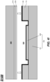
- FIG. 1 is a cross-sectional view of a device 1000 having a cavity 500 , according to an embodiment of the present disclosure.
- device 1000 includes a device wafer 100 including a first substrate 101 and a device structure 300 disposed on first substrate 101 , a first dielectric layer 110 , a second dielectric layer 120 , a second substrate (also referred to as a “cap wafer”) 200 , a trap rich layer 210 , and a buffer layer 220 .
- Device structure 300 may include at least a portion of a semiconductor device or a microelectromechanical system (MEMS) device.
- device structure 300 may include at least a portion of at least one of a film bulk acoustic resonator (FBAR) resonator or filter, a MEMS microphone, a pressure sensor, an acceleration sensor, or a piezoelectric micromachined ultrasonic transducer (PMUT), or another device having a cavity structure.
- FBAR film bulk acoustic resonator
- PMUT piezoelectric micromachined ultrasonic transducer
- First dielectric layer 110 is disposed on first substrate 101 at both ends of device structure 300 .
- First dielectric layer 110 is separated from both ends of device structure 300 with a predetermined distance.
- First dielectric layer 110 forms sidewalls of cavity 500 .
- Second dielectric layer 120 covers the top surface and side surfaces of first dielectric layer 110 , the top surface and side surfaces of device structure 300 , and a portion of the top surface of first substrate 101 between device structure 300 and first dielectric layer 110 .
- Trap rich layer 210 is disposed below second substrate 200 .
- Buffer layer 220 is disposed below trap rich layer 210 .
- Second substrate 200 is bonded to second dielectric layer 120 disposed on device wafer 100 through buffer layer 220 to form cavity 500 .
- FIGS. 2 A- 2 I are cross-sectional views of structures formed in a process of fabricating a device having a cavity, according to a comparative example.
- step S 0 device wafer 100 is obtained.
- Device wafer 100 includes first substrate 101 and device structure 300 formed on first substrate 101 .
- Device structure 300 may include at least a portion of the device having the cavity to be fabricated.
- the device may be a semiconductor device or a microelectromechanical system (MEMS) device, which may include at least one of a film bulk acoustic resonator (FBAR) resonator or filter, a MEMS microphone, a pressure sensor, an acceleration sensor, or a piezoelectric micromachined ultrasonic transducer (PMUT), or another device having a cavity structure.
- MEMS microelectromechanical system
- first dielectric layer 110 is deposited on device wafer 100 .
- First dielectric layer 110 may be formed of silicon, silicon oxide, silicon nitride, aluminum nitride, silicon oxynitride, or other materials, or a stacked combination of two or more of those materials.
- step S 2 the top surface of first dielectric layer 110 is planarized by, for example, a chemical mechanical polishing (CMP) process. As a result, the top surface of first dielectric layer 110 is parallel to the top surface of first substrate 101 .
- CMP chemical mechanical polishing
- a photolithography process is performed. Specifically, first, a photoresist layer 400 is coated on the structure of FIG. 2 C . Photoresist layer 400 is exposed to a light with a mask (not shown) having a certain pattern, and the exposed photoresist layer is developed by a solvent, thereby transferring the pattern of the mask onto photoresist layer 400 . Photoresist layer 400 exposes a part of first dielectric layer 110 that needs to be removed.
- first dielectric layer 110 is etched by using photoresist layer 400 as an etching mask, to expose at least a part of device structure 300 and a part of first substrate 101 , thereby forming a space for forming cavity 500 (herein after referred to as “cavity space 500 ”).
- step S 5 photoresist layer 400 is removed, and the remaining structure is cleaned.
- the surface of first dielectric layer 110 has undergone a series of processes such as photolithography, etching, and cleaning, and thus the surface property of first dielectric layer 110 changes.
- the surface of first dielectric layer 110 no longer has abundant unsaturated bonds, or the surface of first dielectric layer 110 is “contaminated” by the organic molecules in the series of processes.
- the surface of first dielectric layer 110 no longer has the same bonding activeness as when CMP is just completed. If first dielectric layer 110 having such a surface is directly bonded to second substrate 200 , first dielectric layer 110 may not be effectively bonded to second substrate 200 , or at least the bonding strength may be weak.
- step S 6 a slight CMP treatment is performed on the surface of first dielectric layer 110 to remove the part of the surface layer of first dielectric layer 110 that is not suitable for bonding, thereby restoring the bonding activeness of the surface of first dielectric layer 110 .
- the CMP process might cause a portion of the surface of first dielectric layer 110 close to cavity 500 to be inclined to form an inclined surface 110 a.
- step S 7 second substrate 200 is bonded to device wafer 100 via first dielectric layer 110 .
- inclined surface 110 a might not be bonded with second substrate 200 , thereby reducing the effective bonding area, weakening the bonding strength, and causing device reliability problems.
- FIG. 3 is a flow chart of a process 1100 of fabricating device 1000 of FIG. 1 , according to an embodiment of the present disclosure.
- FIGS. 4 A- 4 J are cross-sectional views of structures formed in process 1100 , according to an embodiment of the present disclosure.
- step S 100 device wafer 100 is obtained.
- Device wafer 100 includes first substrate 101 and device structure 300 formed on first substrate 101 .
- Device structure 300 may include at least a portion of the device having the cavity to be fabricated.
- the device may be a semiconductor device or a microelectromechanical system (MEMS) device, which may include at least one of a film bulk acoustic resonator (FBAR) resonator or filter, a MEMS microphone, a pressure sensor, an acceleration sensor, or a piezoelectric micromachined ultrasonic transducer (PMUT), or another device having a cavity structure.
- MEMS microelectromechanical system
- first dielectric layer 110 is deposited on device wafer 100 .
- First dielectric layer 110 may be formed of silicon, silicon oxide, silicon nitride, aluminum nitride, silicon oxynitride, or other materials, or a stacked combination of two or more of those materials.
- step S 102 the top surface of first dielectric layer 110 is planarized by, for example, a chemical mechanical polishing (CMP) process. As a result, the top surface of first dielectric layer 110 is parallel to the top surface of first substrate 101 .
- CMP chemical mechanical polishing
- step S 103 a photolithography process is performed, and first dielectric layer 110 is etched to expose at least a part of device structure 300 and a part of first substrate 101 , thereby forming a space for forming cavity 500 (herein after referred to as “cavity space 500 ”).
- Step S 103 is similar to steps S 3 , S 4 , and S 5 above, and therefore detailed description of step S 103 is not repeated.
- second dielectric layer 120 is deposited on the structure of FIG. 4 D .
- Second dielectric layer 120 covers the top surface and side surfaces of first dielectric layer 110 , and the top surface and side surfaces of device structure 300 .
- Second dielectric layer 120 is a thin layer having a thickness between approximately 10 nm to approximately 100 nm.
- Second dielectric layer 120 may be formed of silicon, silicon oxide, silicon nitride, aluminum nitride, silicon oxynitride, or other materials, or a stacked combination of two or more of those materials.
- Second dielectric layer 120 functions as a protective layer on the surface of device structure 300 to prevent the surface of device structure 300 from being damaged in subsequent processes.
- the material of second dielectric layer 120 may be the same as the material of the surface layer of first dielectric layer 110 .
- the surface of first dielectric layer 110 is not treated by a CMP process. Therefore, the surface of first dielectric layer 110 will not be damaged by the CMP process to form an inclined surface, such as inclined surface 110 a illustrated in FIG. 2 G . Consequently, the entire top surface of first dielectric layer 110 is parallel to the surface of first substrate 101 , and the entire surface of second dielectric layer 120 covering the surface of first dielectric layer 110 is also parallel to the surface of first substrate 101 .
- a surface treatment process is performed on the surface of second dielectric layer 120 to activate the surface of second dielectric layer 120 for bonding.
- the surface treatment process may be a microphysical etching process which may include at least one of air plasma etching, ion beam etching (IBE), or fast atom beam (FAB) etching, or any other physical bombardment processes.
- the surface treatment process removes a surface part of second dielectric layer 120 , so that at least a part of the molecular bonds of the material on the surface of second dielectric layer 120 are broken to facilitate the subsequent bonding process.
- the surface of second dielectric layer 120 is not treated by the CMP process, so the portion of the surface of second dielectric layer 120 close to the boundary of cavity space 500 will not be inclined. Consequently, the entire top surface of second dielectric layer 120 is parallel to the surface of first substrate 101 . As a result, during a subsequent bonding process of bonding second substrate 200 , the entire top surface of second dielectric layer 120 may be effectively bonded to second substrate 200 , which increases the bonding surface area and bonding strength compared to the process described with respect to FIGS. 2 A- 2 I .
- second substrate (cap wafer) 200 is obtained, and trap rich layer 210 is formed on second substrate 200 .
- Second substrate 200 may be formed of a single silicon material.
- Trap rich layer 210 may be formed of polysilicon, amorphous silicon, silicon nitride, aluminum nitride, gallium nitride, or a stacked combination of two or more of those materials.
- buffer layer 220 is formed on trap rich layer 210 , and the surface of buffer layer 220 is polished by using, for example, a CMP surface polishing process, to form a material surface suitable for bonding.
- Buffer layer 220 may be formed of silicon oxide or silicon nitride.
- buffer layer 220 on second substrate 200 and second dielectric layer 120 on device wafer 100 are attached and bonded to form cavity 500 .
- FIG. 5 is a cross-sectional view of a device 2000 having a cavity 600 , according to an embodiment of the present disclosure.
- Device 2000 of FIG. 5 is similar to device 1000 of FIG. 1 , except that portions of second substrate 200 , trap rich layer 210 , and buffer layer 220 that are vertically aligned with cavity space 500 formed on device wafer 100 , are removed, to form a recess 200 a .
- Recess 200 a and cavity space 500 together form cavity 600 . Therefore, the volume of cavity 600 in device 2000 is greater than that of cavity 500 in device 1000 .
- the other components of device 2000 are the same as those of device 1000 , and therefore detailed descriptions of those components are not repeated.
- FIG. 6 is a flow chart of a process 2100 of fabricating device 2000 of FIG. 5 , according to an embodiment of the present disclosure.
- Process 2100 is similar to process 1100 of FIG. 3 , except that additional steps S 150 and S 151 are performed after step S 107 and before step S 108 . Therefore, detailed description of steps S 150 and S 151 is provided below, and detailed description of the other steps is not repeated.
- FIGS. 7 A- 7 D are cross-sectional views of structures formed in steps S 150 , S 151 , and S 108 in process 2100 , according to an embodiment of the present disclosure.
- step S 150 after forming trap rich layer 210 and buffer layer 220 on second substrate 200 , recess 200 a is formed on second substrate 200 by etching buffer layer 220 , trap rich layer 210 , and second substrate 200 .
- a surface treatment process is performed on the surface of buffer layer 220 to remove a portion of buffer layer 220 , so that at least a part of the molecular bonds of the material on the surface of buffer layer 220 are broken, so as to facilitate the subsequent bonding process.
- the surface treatment process may be a microphysical etching process which may include at least one of air plasma etching, ion beam etching (IBE), or fast atom beam (FAB) etching, or any other physical bombardment processes.
- step S 108 buffer layer 220 on second substrate 200 and second dielectric layer 120 on device wafer 100 are attached and bonded.
- recess 200 a formed on second substrate 200 and cavity space 500 formed on device wafer 100 together form cavity 600 .
Abstract
Description
Claims (17)
Applications Claiming Priority (2)
| Application Number | Priority Date | Filing Date | Title |
|---|---|---|---|
| CN202310283676.5A CN116239076A (en) | 2023-03-15 | 2023-03-15 | Method for producing a device with a cavity |
| CN202310283676.5 | 2023-03-15 |
Publications (2)
| Publication Number | Publication Date |
|---|---|
| US20230274945A1 US20230274945A1 (en) | 2023-08-31 |
| US11901193B2 true US11901193B2 (en) | 2024-02-13 |
Family
ID=86624254
Family Applications (1)
| Application Number | Title | Priority Date | Filing Date |
|---|---|---|---|
| US18/315,091 Active US11901193B2 (en) | 2023-03-15 | 2023-05-10 | Fabrication method of device with cavity |
Country Status (2)
| Country | Link |
|---|---|
| US (1) | US11901193B2 (en) |
| CN (1) | CN116239076A (en) |
Families Citing this family (1)
| Publication number | Priority date | Publication date | Assignee | Title |
|---|---|---|---|---|
| CN116683881A (en) * | 2023-07-27 | 2023-09-01 | 深圳新声半导体有限公司 | Preparation method and packaging method of bulk acoustic wave resonator |
Citations (2)
| Publication number | Priority date | Publication date | Assignee | Title |
|---|---|---|---|---|
| US7622324B2 (en) * | 2002-09-25 | 2009-11-24 | Ziptronix | Wafer bonding hermetic encapsulation |
| US10961118B2 (en) * | 2017-11-28 | 2021-03-30 | Taiwan Semiconductor Manufacturing Co., Ltd. | Wafer level integrated MEMS device enabled by silicon pillar and smart cap |
-
2023
- 2023-03-15 CN CN202310283676.5A patent/CN116239076A/en active Pending
- 2023-05-10 US US18/315,091 patent/US11901193B2/en active Active
Patent Citations (2)
| Publication number | Priority date | Publication date | Assignee | Title |
|---|---|---|---|---|
| US7622324B2 (en) * | 2002-09-25 | 2009-11-24 | Ziptronix | Wafer bonding hermetic encapsulation |
| US10961118B2 (en) * | 2017-11-28 | 2021-03-30 | Taiwan Semiconductor Manufacturing Co., Ltd. | Wafer level integrated MEMS device enabled by silicon pillar and smart cap |
Also Published As
| Publication number | Publication date |
|---|---|
| CN116239076A (en) | 2023-06-09 |
| US20230274945A1 (en) | 2023-08-31 |
Similar Documents
| Publication | Publication Date | Title |
|---|---|---|
| US8012785B2 (en) | Method of fabricating an integrated CMOS-MEMS device | |
| US10490728B2 (en) | Fabrication methods for a piezoelectric micro-electromechanical system (MEMS) | |
| TWI495049B (en) | Method for manufacturing microelectronic device and integrated circuit to prevent metal pad damage in wafer level package | |
| US9172025B2 (en) | Integrated semiconductor devices with single crystalline beam, methods of manufacture and design structure | |
| US11901193B2 (en) | Fabrication method of device with cavity | |
| US8629036B2 (en) | Integrated semiconductor devices with amorphous silicon beam, methods of manufacture and design structure | |
| US7239067B2 (en) | Method of manufacturing a piezoelectric thin film resonator, manufacturing apparatus for a piezoelectric thin film resonator, piezoelectric thin film resonator, and electronic component | |
| US20210111701A1 (en) | Bulk Resonator with Symmetrically Positioned Temperature Compensation Layers | |
| US9105751B2 (en) | Integrated semiconductor devices with single crystalline beam, methods of manufacture and design structure | |
| JP5877907B2 (en) | MEMS microphone with reduced parasitic capacitance | |
| US9181081B2 (en) | Electrical component and method of manufacturing the same | |
| CN112039485A (en) | Thin film piezoelectric acoustic wave filter and manufacturing method thereof | |
| WO2020177558A1 (en) | Packaging of mems device having release hole outside packaging space | |
| US6242363B1 (en) | Method of etching a wafer layer using a sacrificial wall to form vertical sidewall | |
| US20230299737A1 (en) | Bulk acoustic wave resonator and fabrication method thereof | |
| US11706987B2 (en) | Semiconductor device and method of forming a semiconductor device | |
| US11463070B2 (en) | FBAR structure and manufacturing method of same | |
| WO2023173900A1 (en) | Bulk acoustic resonator, filter, and manufacturing methods therefor | |
| US11616489B2 (en) | Bulk acoustic wave filter having release hole and fabricating method of the same | |
| US20220393662A1 (en) | Bulk acoustic wave filter having release hole and fabricating method of the same | |
| CN114978093A (en) | Acoustic wave resonator, filter, communication apparatus, and method of manufacturing the same | |
| JP7111406B2 (en) | Fabrication method of thin film bulk acoustic wave resonator | |
| JP4259019B2 (en) | Manufacturing method of electronic parts | |
| US11689171B2 (en) | Bulk acoustic wave resonator and fabrication method thereof | |
| US20230091476A1 (en) | Bulk acoustic wave resonator with metal bonding layer |
Legal Events
| Date | Code | Title | Description |
|---|---|---|---|
| AS | Assignment |
Owner name: SHENZHEN NEWSONIC TECHNOLOGIES CO., LTD., CHINA Free format text: ASSIGNMENT OF ASSIGNORS INTEREST;ASSIGNOR:WENG, GUOJUN;REEL/FRAME:063597/0348 Effective date: 20230420 |
|
| FEPP | Fee payment procedure |
Free format text: ENTITY STATUS SET TO UNDISCOUNTED (ORIGINAL EVENT CODE: BIG.); ENTITY STATUS OF PATENT OWNER: SMALL ENTITY |
|
| FEPP | Fee payment procedure |
Free format text: ENTITY STATUS SET TO SMALL (ORIGINAL EVENT CODE: SMAL); ENTITY STATUS OF PATENT OWNER: SMALL ENTITY |
|
| STPP | Information on status: patent application and granting procedure in general |
Free format text: SPECIAL NEW |
|
| STPP | Information on status: patent application and granting procedure in general |
Free format text: NOTICE OF ALLOWANCE MAILED -- APPLICATION RECEIVED IN OFFICE OF PUBLICATIONS |
|
| STPP | Information on status: patent application and granting procedure in general |
Free format text: AWAITING TC RESP., ISSUE FEE NOT PAID |
|
| STPP | Information on status: patent application and granting procedure in general |
Free format text: NOTICE OF ALLOWANCE MAILED -- APPLICATION RECEIVED IN OFFICE OF PUBLICATIONS |
|
| STPP | Information on status: patent application and granting procedure in general |
Free format text: PUBLICATIONS -- ISSUE FEE PAYMENT RECEIVED |
|
| STPP | Information on status: patent application and granting procedure in general |
Free format text: PUBLICATIONS -- ISSUE FEE PAYMENT VERIFIED |
|
| STCF | Information on status: patent grant |
Free format text: PATENTED CASE |