US11899951B2 - Error restoring method, microcontroller unit using the same, and battery device including the microcontroller unit - Google Patents
Error restoring method, microcontroller unit using the same, and battery device including the microcontroller unit Download PDFInfo
- Publication number
- US11899951B2 US11899951B2 US17/279,862 US202017279862A US11899951B2 US 11899951 B2 US11899951 B2 US 11899951B2 US 202017279862 A US202017279862 A US 202017279862A US 11899951 B2 US11899951 B2 US 11899951B2
- Authority
- US
- United States
- Prior art keywords
- application
- mcu
- flash memory
- key value
- reprogramming
- Prior art date
- Legal status (The legal status is an assumption and is not a legal conclusion. Google has not performed a legal analysis and makes no representation as to the accuracy of the status listed.)
- Active, expires
Links
Images


Classifications
-
- G—PHYSICS
- G06—COMPUTING OR CALCULATING; COUNTING
- G06F—ELECTRIC DIGITAL DATA PROCESSING
- G06F3/00—Input arrangements for transferring data to be processed into a form capable of being handled by the computer; Output arrangements for transferring data from processing unit to output unit, e.g. interface arrangements
- G06F3/06—Digital input from, or digital output to, record carriers, e.g. RAID, emulated record carriers or networked record carriers
- G06F3/0601—Interfaces specially adapted for storage systems
- G06F3/0628—Interfaces specially adapted for storage systems making use of a particular technique
- G06F3/0629—Configuration or reconfiguration of storage systems
- G06F3/0634—Configuration or reconfiguration of storage systems by changing the state or mode of one or more devices
-
- G—PHYSICS
- G06—COMPUTING OR CALCULATING; COUNTING
- G06F—ELECTRIC DIGITAL DATA PROCESSING
- G06F11/00—Error detection; Error correction; Monitoring
- G06F11/07—Responding to the occurrence of a fault, e.g. fault tolerance
- G06F11/14—Error detection or correction of the data by redundancy in operations
- G06F11/1402—Saving, restoring, recovering or retrying
- G06F11/1415—Saving, restoring, recovering or retrying at system level
- G06F11/1441—Resetting or repowering
-
- G—PHYSICS
- G06—COMPUTING OR CALCULATING; COUNTING
- G06F—ELECTRIC DIGITAL DATA PROCESSING
- G06F11/00—Error detection; Error correction; Monitoring
- G06F11/07—Responding to the occurrence of a fault, e.g. fault tolerance
- G06F11/0703—Error or fault processing not based on redundancy, i.e. by taking additional measures to deal with the error or fault not making use of redundancy in operation, in hardware, or in data representation
- G06F11/0706—Error or fault processing not based on redundancy, i.e. by taking additional measures to deal with the error or fault not making use of redundancy in operation, in hardware, or in data representation the processing taking place on a specific hardware platform or in a specific software environment
-
- G—PHYSICS
- G06—COMPUTING OR CALCULATING; COUNTING
- G06F—ELECTRIC DIGITAL DATA PROCESSING
- G06F11/00—Error detection; Error correction; Monitoring
- G06F11/07—Responding to the occurrence of a fault, e.g. fault tolerance
- G06F11/0703—Error or fault processing not based on redundancy, i.e. by taking additional measures to deal with the error or fault not making use of redundancy in operation, in hardware, or in data representation
- G06F11/0751—Error or fault detection not based on redundancy
-
- G—PHYSICS
- G06—COMPUTING OR CALCULATING; COUNTING
- G06F—ELECTRIC DIGITAL DATA PROCESSING
- G06F11/00—Error detection; Error correction; Monitoring
- G06F11/07—Responding to the occurrence of a fault, e.g. fault tolerance
- G06F11/0703—Error or fault processing not based on redundancy, i.e. by taking additional measures to deal with the error or fault not making use of redundancy in operation, in hardware, or in data representation
- G06F11/0793—Remedial or corrective actions
-
- G—PHYSICS
- G06—COMPUTING OR CALCULATING; COUNTING
- G06F—ELECTRIC DIGITAL DATA PROCESSING
- G06F11/00—Error detection; Error correction; Monitoring
- G06F11/07—Responding to the occurrence of a fault, e.g. fault tolerance
- G06F11/14—Error detection or correction of the data by redundancy in operations
- G06F11/1402—Saving, restoring, recovering or retrying
- G06F11/1415—Saving, restoring, recovering or retrying at system level
- G06F11/1417—Boot up procedures
-
- G—PHYSICS
- G06—COMPUTING OR CALCULATING; COUNTING
- G06F—ELECTRIC DIGITAL DATA PROCESSING
- G06F11/00—Error detection; Error correction; Monitoring
- G06F11/07—Responding to the occurrence of a fault, e.g. fault tolerance
- G06F11/14—Error detection or correction of the data by redundancy in operations
- G06F11/1402—Saving, restoring, recovering or retrying
- G06F11/1415—Saving, restoring, recovering or retrying at system level
- G06F11/142—Reconfiguring to eliminate the error
-
- G—PHYSICS
- G06—COMPUTING OR CALCULATING; COUNTING
- G06F—ELECTRIC DIGITAL DATA PROCESSING
- G06F11/00—Error detection; Error correction; Monitoring
- G06F11/07—Responding to the occurrence of a fault, e.g. fault tolerance
- G06F11/16—Error detection or correction of the data by redundancy in hardware
- G06F11/1666—Error detection or correction of the data by redundancy in hardware where the redundant component is memory or memory area
-
- G—PHYSICS
- G06—COMPUTING OR CALCULATING; COUNTING
- G06F—ELECTRIC DIGITAL DATA PROCESSING
- G06F3/00—Input arrangements for transferring data to be processed into a form capable of being handled by the computer; Output arrangements for transferring data from processing unit to output unit, e.g. interface arrangements
- G06F3/06—Digital input from, or digital output to, record carriers, e.g. RAID, emulated record carriers or networked record carriers
- G06F3/0601—Interfaces specially adapted for storage systems
- G06F3/0602—Interfaces specially adapted for storage systems specifically adapted to achieve a particular effect
- G06F3/0614—Improving the reliability of storage systems
- G06F3/0619—Improving the reliability of storage systems in relation to data integrity, e.g. data losses, bit errors
-
- G—PHYSICS
- G06—COMPUTING OR CALCULATING; COUNTING
- G06F—ELECTRIC DIGITAL DATA PROCESSING
- G06F3/00—Input arrangements for transferring data to be processed into a form capable of being handled by the computer; Output arrangements for transferring data from processing unit to output unit, e.g. interface arrangements
- G06F3/06—Digital input from, or digital output to, record carriers, e.g. RAID, emulated record carriers or networked record carriers
- G06F3/0601—Interfaces specially adapted for storage systems
- G06F3/0602—Interfaces specially adapted for storage systems specifically adapted to achieve a particular effect
- G06F3/062—Securing storage systems
- G06F3/0623—Securing storage systems in relation to content
-
- G—PHYSICS
- G06—COMPUTING OR CALCULATING; COUNTING
- G06F—ELECTRIC DIGITAL DATA PROCESSING
- G06F3/00—Input arrangements for transferring data to be processed into a form capable of being handled by the computer; Output arrangements for transferring data from processing unit to output unit, e.g. interface arrangements
- G06F3/06—Digital input from, or digital output to, record carriers, e.g. RAID, emulated record carriers or networked record carriers
- G06F3/0601—Interfaces specially adapted for storage systems
- G06F3/0628—Interfaces specially adapted for storage systems making use of a particular technique
- G06F3/0655—Vertical data movement, i.e. input-output transfer; data movement between one or more hosts and one or more storage devices
- G06F3/0658—Controller construction arrangements
-
- G—PHYSICS
- G06—COMPUTING OR CALCULATING; COUNTING
- G06F—ELECTRIC DIGITAL DATA PROCESSING
- G06F3/00—Input arrangements for transferring data to be processed into a form capable of being handled by the computer; Output arrangements for transferring data from processing unit to output unit, e.g. interface arrangements
- G06F3/06—Digital input from, or digital output to, record carriers, e.g. RAID, emulated record carriers or networked record carriers
- G06F3/0601—Interfaces specially adapted for storage systems
- G06F3/0668—Interfaces specially adapted for storage systems adopting a particular infrastructure
- G06F3/0671—In-line storage system
- G06F3/0673—Single storage device
- G06F3/0679—Non-volatile semiconductor memory device, e.g. flash memory, one time programmable memory [OTP]
-
- H02J7/0063—
-
- H—ELECTRICITY
- H02—GENERATION; CONVERSION OR DISTRIBUTION OF ELECTRIC POWER
- H02J—ELECTRIC POWER NETWORKS; CIRCUIT ARRANGEMENTS OR SYSTEMS FOR SUPPLYING OR DISTRIBUTING ELECTRIC POWER; SYSTEMS FOR STORING ELECTRIC ENERGY
- H02J7/00—Circuit arrangements for charging or discharging batteries or for supplying loads from batteries
- H02J7/855—Circuit arrangements for charging or discharging batteries or for supplying loads from batteries with circuits adapted for supplying loads from the battery
-
- H—ELECTRICITY
- H02—GENERATION; CONVERSION OR DISTRIBUTION OF ELECTRIC POWER
- H02J—ELECTRIC POWER NETWORKS; CIRCUIT ARRANGEMENTS OR SYSTEMS FOR SUPPLYING OR DISTRIBUTING ELECTRIC POWER; SYSTEMS FOR STORING ELECTRIC ENERGY
- H02J9/00—Circuit arrangements for emergency or stand-by power supply, e.g. for emergency lighting
- H02J9/002—Circuit arrangements for emergency or stand-by power supply, e.g. for emergency lighting in which a reserve is maintained in an energy source by disconnecting non-critical loads, e.g. maintaining a reserve of charge in a vehicle battery for starting an engine
-
- G—PHYSICS
- G06—COMPUTING OR CALCULATING; COUNTING
- G06F—ELECTRIC DIGITAL DATA PROCESSING
- G06F3/00—Input arrangements for transferring data to be processed into a form capable of being handled by the computer; Output arrangements for transferring data from processing unit to output unit, e.g. interface arrangements
- G06F3/06—Digital input from, or digital output to, record carriers, e.g. RAID, emulated record carriers or networked record carriers
- G06F3/0601—Interfaces specially adapted for storage systems
- G06F3/0602—Interfaces specially adapted for storage systems specifically adapted to achieve a particular effect
- G06F3/0604—Improving or facilitating administration, e.g. storage management
- G06F3/0605—Improving or facilitating administration, e.g. storage management by facilitating the interaction with a user or administrator
Definitions
- the present disclosure relates to an error restoring method, a microcontroller unit using the error restoring method, and a battery device including the microcontroller.
- ECC error correction code
- An error restoring method of a flash memory, a micro controller unit using the error restoring method of the flash memory, and a battery device including the micro controller unit can be provided.
- a micro controller unit includes a flash memory, wherein the flash memory may be configured to determine a key value of an application stored in the flash memory when the MCU is powered on, and, when the key value of the application is invalid, the flash memory may enter a mode that enables reprogramming of the flash memory.
- the flash memory may include a flash boot loader (FBL), an application block, and an application key block, when the MCU is powered on the flash boot loader may be configured to determine the application key value in the application key block, and, the mode that enables reprogramming is a flash boot loader mode.
- FBL flash boot loader
- the application block may be configured to reprogram received application data in the flash boot loader mode.
- the application block may be configured to write a valid application key value after completion of the reprogramming.
- the flash memory may be configured to, when receiving a reprograming request, erase a key value of an application that corresponds to the reprograming request, and may enter the mode.
- the flash memory may be configured to reprogram received application data and may be configured to write an application key value in the mode.
- an error restoring method of a microcontroller unit that includes a flash memory, the flash memory including a flash boot loader, an application block, and an application key block.
- the error restoring method includes: when the MCU is powered on, determining, by the flash boot loader, an application key value in the application key block; and when the application key value is invalid in the determining the application key value, staying in the flash boot loader for enabling reprogramming of the flash memory.
- the error restoring method of the MCU may further include, reprogramming received application data and writing a valid application key value after completion of the reprogramming.
- the error restoring method of the MCU may further include: in the determining the application key value, executing a corresponding application when the application key value is valid; receiving a reprogramming request during execution of the corresponding application; and erasing a key value of the corresponding application when receiving the reprogramming request.
- the error restoring method may be performed from the determining of the application key value in the application key block, by the flash boot loader.
- a battery device includes: a battery cell assembly that includes a plurality of battery cells that are electrically connected to each other, a micro controller unit (MCU) that includes a flash memory, the flash memory being configured to store an application for battery management of the battery cell assembly; and a battery management system that performs the battery management according to the application executed by the MCU.
- MCU micro controller unit
- the flash memory may be configured to determine a key value of the application, and when the key value of the application is invalid, the flash memory may be configured to enter a mode that enables reprogramming of the flash memory.
- An error restoring method of a flash memory, a micro controller unit using the error restoring method of the flash memory, and a battery device including the micro controller unit may be provided.
- FIG. 1 shows a microcontroller unit according to an exemplary embodiment.
- FIG. 2 shows a configuration of the flash memory according to the exemplary embodiment.
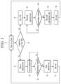
- FIG. 3 is a flowchart of a restoring method according to an exemplary embodiment.
- FIG. 4 shows a battery device according to an exemplary embodiment.
- FIG. 1 shows a microcontroller unit according to an exemplary embodiment.
- a microcontroller unit (MCU) 1 includes a flash memory 2 , a processor 3 , and a peripheral device 4 .
- the flash memory 2 stores an application that is required by a device to which the MCU 1 is applied, executes software of the application, reprograms the corresponding software when reprogramming is requested, and deletes and resets an application key area when a CPU core exception occurs due to an ECC error and the error has occurred in the key application area such that the flash memory 2 may operate in a state of being capable of reprogramming.
- the processor 3 may transmit information input through the peripheral device 4 to the flash memory 2 while networking with the flash memory 2 and the peripheral device 4 through an interface, and may transmit commands to control operations of the flash memory 2 and the peripheral device 4 .
- a power-on signal P_ON is input to the processor 3 , and the processor 3 transmits commands for execution of an application to the flash memory 2 .
- the peripheral device 4 includes a communication module for CAN communication, UART communication, and the like, and transmits a reprogramming request and software codes for reprogramming to the processor 3 .
- FIG. 2 shows a configuration of the flash memory 2 according to the exemplary embodiment.
- the flash memory 2 includes a flash bootloader (FBL) 21 , an application block 22 , and an application key block 23 .
- FBL flash bootloader
- the FBL 21 may erase software in an application area of the flash memory 2 and perform reprogramming.
- the FBL 21 may determine whether a key value of the application is valid according to the command transmitted from the processor 3 .
- the key value of the application is not valid according to a determination result of the FBL 21 , the application of the application block 22 is not executed, and the flash memory 2 enters the FBL mode.
- the FBL 21 may inform the processor 3 that the application key value is invalid.
- the application block 22 can operate the software stored in the application area according to a command.
- the application key block 23 erases and resets an application key area corresponding to the active application, and then the flash memory 2 enters the FBL mode.
- the flash memory 2 enters the FBL mode where the command stays in the FBL 21 for reprogramming.
- the FBL 21 receives data with respect to an application corresponding to a command from the peripheral device 4 through CAN communication or UART communication, and performs reprogramming of the received data in the application block 22 area. After the received data is written into the application area through reprogramming, the application key block 23 writes a valid key value into an area corresponding to the application. After the writing, the application key block 23 performs reset, and the application block 22 may perform a reprogrammed application through the corresponding reset.
- the FBL 21 erases and resets the application key value when the ECC error is generated in the application key block 23 such that the flash memory 2 enters the FBL mode. That is, the flash memory 2 enters the FBL mode, which is restored to a state that reprogramming is possible.
- the FBL 21 , the application block 22 , and the application key block 23 may transmit and receive necessary information to and from each other.
- FIG. 3 is a flowchart of a restoring method according to an exemplary embodiment.
- the MCU 1 may be powered on or reset (step S 1 ).
- the FBL 21 may determine whether a key value of an application that needs to be operated according to a command of the processor is valid (step S 2 ).
- the command may be transmitted to the application block 22 from the FBL 21 (step S 3 ).
- the application block 22 may perform the corresponding application according to the command (step S 4 ).
- step S 5 it may be determined whether there is a reprogramming request.
- the application key block 23 may erase the key value of the corresponding application (step S 6 ).
- soft reset may be carried out (step S 7 ).
- the execution of the application may be stopped due to the soft reset.
- the application execution may be maintained according to the step S 4 .
- step S 7 the flash memory 2 enters the FBL mode again, and the process may be carried out from the step S 2 . Then, since the application key value is invalid, the reprogramming is carried out in the FBL mode such that a valid application key value may be written.
- a command may stay in the FBL 21 (step S 8 ). That is, the flash memory 2 enters the FBL mode. In this case, a CPU core exception due to an ECC error may occur.
- the FBL 21 may reprogram an application area (step S 9 ).
- the application block 22 may determine whether the reprogramming is completed (step S 10 ).
- step S 9 When it determined that the reprogramming is not completed in the step S 10 , the execution of the step S 9 may be maintained.
- the application key block 23 may write a valid application key value (step S 11 ).
- step S 12 soft reset may be carried out.
- the flash memory 2 enters the FBL mode according to the step S 1 and then the process may be carried out from the step S 2 again.
- FIG. 4 shows a battery device according to an exemplary embodiment.
- a battery device 100 includes an MCU 120 , and the MCU 120 may store a plurality of applications required for battery monitoring and management.
- the battery device 100 may be driven according to an application executed by the MCU 120 .
- the MCU 120 may include an application for estimating a state of charge and lifespan of a battery pack and state information such as current, voltage, temperature, and the like of the battery pack and battery cell.
- an application for estimation of a state of charge (SOC) of the battery pack may be executed in the MCU 120 , and an application for detecting battery state information for estimation of the SOC of the battery pack may be executed.
- SOC state of charge
- the battery device 100 includes a battery management system (BMS) 110 , the micro controller unit (MCU) 120 , a battery cell assembly 130 , and relays 140 and 150 .
- BMS battery management system
- MCU micro controller unit
- the battery cell assembly 130 includes a plurality of battery cells that are electrically connected.
- a battery module in which a predetermined number of battery cells are connected in series is formed, and a predetermined number of battery modules are connected in series and in parallel such that desired power can be supplied.
- Each of the plurality of battery cells that form the battery cell assembly 130 are electrically connected with the BMS 110 through a plurality of wires.
- the BMS 110 collects and analyzes various pieces of information related to the battery device that include information on a plurality of battery cells to control charging/discharging of the battery device, battery cell balancing, a protection operation, and the like.
- the relays 140 and 150 may be implemented as a relay or an n-channel type of transistor, and are connected in series between the battery cell assembly 130 and an external device. Each of the relays 140 and 150 may operate by a signal supplied from the BMS 110 .
- the MCU 120 may be implemented according to the above-described exemplary embodiment.
- a control signal according to the application may be transmitted to the BMS 110 .
- the BMS 110 may operate according to the application executed in the MCU 120 .
- the BMS 110 estimates a SOC according to the application.
- An estimation method of the SOC is determined according to the application.
- an SOC estimation application may estimate a SOC (hereinafter, referred to as a first SOC) by using a first battery modeling method and may estimate a SOC (hereinafter, referred to as a second SOC) by using a second battery modeling method, and the first battery modelling method and the second battery modeling method may be different from each other.
- the battery modeling method is one that is used to estimate a state of a battery having a non-linear characteristic, and may include an electrical circuit model, an electrochemical model, an analytical model, and a stochastic model.
- the BMS 110 may estimate a first SOC at the present stage based on a SOC estimated at the previous stage and information included in battery cell assembly state information by using an electrical circuit model as the first battery modeling method according to the SOC estimation application.
- an electrochemical model may be used as the second battery modeling.
- the electrical circuit model is a method for modeling input and output characteristics of a battery using an equivalent circuit implemented as an electrical circuit.
- the electrical circuit model has a merit that an operation process for SOC estimation is relatively simple, so that time required for the operation is not long and the load for the operation is not excessive.
- accuracy is somewhat lower.
- the electrochemical model is a method for modeling the characteristic of a battery based on a chemical action occurring inside the battery.
- a representative example of such an electrochemical model is a Doyle-Fuller-Newman (DFN) model.
- the DFN model may model spatial and temporal changes in the lithium ion concentration present in a porous electrode, potential, intercalation kinetics, and current density between solid and electrolyte solution phases.
- Such an electrochemical model has a merit of very high accuracy.
- the BMS 110 may acquire a highly accurate SOC estimation value (i.e., second SOC) based on state information of a battery cell assembly by using an electrical chemical model such as a DFN model according to the SOC estimation application.
- the BMS 110 may increase accuracy of the SOC (first SOC) estimation by reflecting the SOC estimation result (second SOC) with high accuracy according to the SOC estimation application in an input parameter.
- the BMS 110 may recognize the second SOC value as a first SOC of the previous stage according to the SOC estimation application, and may estimate a first SOC of the present stage by applying the received state information of the battery cell assembly and the first SOC of the previous stage to the first battery modeling method. Then, the first SOC value can be periodically corrected such that an error in the first SOC estimation can be periodically prevented from increasing, thereby improving accuracy in the SOC estimation.
Landscapes
- Engineering & Computer Science (AREA)
- Theoretical Computer Science (AREA)
- Physics & Mathematics (AREA)
- General Engineering & Computer Science (AREA)
- General Physics & Mathematics (AREA)
- Quality & Reliability (AREA)
- Human Computer Interaction (AREA)
- Power Engineering (AREA)
- Emergency Management (AREA)
- Business, Economics & Management (AREA)
- Computer Security & Cryptography (AREA)
- Techniques For Improving Reliability Of Storages (AREA)
- Charge And Discharge Circuits For Batteries Or The Like (AREA)
- Microcomputers (AREA)
- Memory System (AREA)
- Stored Programmes (AREA)
Abstract
Description
Claims (11)
Applications Claiming Priority (3)
| Application Number | Priority Date | Filing Date | Title |
|---|---|---|---|
| KR1020190003998A KR102711942B1 (en) | 2019-01-11 | 2019-01-11 | Error restoration method and micro controller unit using the same, and battery device comprsing the micro controller unit |
| KR10-2019-0003998 | 2019-01-11 | ||
| PCT/KR2020/000511 WO2020145742A1 (en) | 2019-01-11 | 2020-01-10 | Error recovery method, micro controller unit using same, and battery device including micro controller unit |
Publications (2)
| Publication Number | Publication Date |
|---|---|
| US20220035545A1 US20220035545A1 (en) | 2022-02-03 |
| US11899951B2 true US11899951B2 (en) | 2024-02-13 |
Family
ID=71521830
Family Applications (1)
| Application Number | Title | Priority Date | Filing Date |
|---|---|---|---|
| US17/279,862 Active 2040-12-18 US11899951B2 (en) | 2019-01-11 | 2020-01-10 | Error restoring method, microcontroller unit using the same, and battery device including the microcontroller unit |
Country Status (6)
| Country | Link |
|---|---|
| US (1) | US11899951B2 (en) |
| EP (1) | EP3848810B1 (en) |
| JP (1) | JP7207818B2 (en) |
| KR (1) | KR102711942B1 (en) |
| CN (1) | CN112771503B (en) |
| WO (1) | WO2020145742A1 (en) |
Families Citing this family (2)
| Publication number | Priority date | Publication date | Assignee | Title |
|---|---|---|---|---|
| CN115454332B (en) * | 2022-08-16 | 2025-10-10 | 均胜群英(南京)新能源汽车系统研究院有限公司 | A method for adaptively storing electric energy for a vehicle-mounted charging pile |
| EP4675477A1 (en) * | 2024-07-01 | 2026-01-07 | STMicroelectronics International N.V. | Method for configuring a microcontroller and corresponding microcontroller |
Citations (16)
| Publication number | Priority date | Publication date | Assignee | Title |
|---|---|---|---|---|
| US20020126528A1 (en) | 2000-12-28 | 2002-09-12 | Sandisk Corporation | Novel method and structure for efficient data verification operation for non-volatile memories |
| US20040078119A1 (en) * | 2002-08-05 | 2004-04-22 | Luitje William V. | Flash loader for vehicle electronic control units |
| US20080086631A1 (en) | 2000-01-06 | 2008-04-10 | Chow David Q | Flash memory controller controlling various flash memory cells |
| US20090199048A1 (en) | 2008-02-04 | 2009-08-06 | Honeywell International Inc. | System and method for detection and prevention of flash corruption |
| JP2011083147A (en) | 2009-10-08 | 2011-04-21 | Lenovo Singapore Pte Ltd | Battery pack, firmware updating method for the same, and battery-pack system |
| JP2011164827A (en) | 2010-02-08 | 2011-08-25 | Nippon Avionics Co Ltd | Electronic apparatus including flash memory and method for updating program stored in flash memory |
| US20120054541A1 (en) | 2010-08-31 | 2012-03-01 | Apple Inc. | Handling errors during device bootup from a non-volatile memory |
| US20130055046A1 (en) | 2011-08-31 | 2013-02-28 | Greg A. Blodgett | Memory refresh methods and apparatuses |
| JP5597224B2 (en) | 2012-05-11 | 2014-10-01 | 株式会社東芝 | Information storage device and memory abnormality processing method |
| US20140310698A1 (en) | 2013-04-10 | 2014-10-16 | Pantech Co., Ltd. | Apparatus and method for upgrading firmware of mobile terminal |
| US20150067314A1 (en) | 2013-08-30 | 2015-03-05 | Timothy J. Strauss | Secure firmware flash controller |
| US9280654B1 (en) * | 2012-08-17 | 2016-03-08 | Electrochem Solutions, Inc. | Battery authentication circuit |
| JP2016081341A (en) | 2014-10-17 | 2016-05-16 | 株式会社デンソー | Electronic control device |
| KR20160144762A (en) | 2015-06-09 | 2016-12-19 | (주) 비엠지 | Remote controlling system for battery |
| US20170024221A1 (en) * | 2013-12-13 | 2017-01-26 | Ping He | Devices, updaters, methods for controlling a device, and methods for controlling an updater |
| KR101744998B1 (en) | 2011-08-26 | 2017-06-21 | 현대자동차주식회사 | Re-programming control module and re-programming system and method using the re-programming control module |
-
2019
- 2019-01-11 KR KR1020190003998A patent/KR102711942B1/en active Active
-
2020
- 2020-01-10 JP JP2021513394A patent/JP7207818B2/en active Active
- 2020-01-10 WO PCT/KR2020/000511 patent/WO2020145742A1/en not_active Ceased
- 2020-01-10 EP EP20738932.1A patent/EP3848810B1/en active Active
- 2020-01-10 CN CN202080005416.6A patent/CN112771503B/en active Active
- 2020-01-10 US US17/279,862 patent/US11899951B2/en active Active
Patent Citations (29)
| Publication number | Priority date | Publication date | Assignee | Title |
|---|---|---|---|---|
| US20080086631A1 (en) | 2000-01-06 | 2008-04-10 | Chow David Q | Flash memory controller controlling various flash memory cells |
| US20020126528A1 (en) | 2000-12-28 | 2002-09-12 | Sandisk Corporation | Novel method and structure for efficient data verification operation for non-volatile memories |
| KR20030068202A (en) | 2000-12-28 | 2003-08-19 | 쌘디스크 코포레이션 | Novel method and structure for efficient data verification operation for non-volatile memories |
| US20030174555A1 (en) | 2000-12-28 | 2003-09-18 | Sandisk Corporation | Novel method and structure for efficient data verification operation for non-volatile memories |
| US20050195653A1 (en) | 2000-12-28 | 2005-09-08 | Conley Kevin M. | Novel method and structure for efficient data verification operation for non-volatile memories |
| US20070109858A1 (en) | 2000-12-28 | 2007-05-17 | Conley Kevin M | Novel Method and Structure for Efficient Data Verification Operation for Non-Volatile Memories |
| US20040078119A1 (en) * | 2002-08-05 | 2004-04-22 | Luitje William V. | Flash loader for vehicle electronic control units |
| US20090199048A1 (en) | 2008-02-04 | 2009-08-06 | Honeywell International Inc. | System and method for detection and prevention of flash corruption |
| JP2011083147A (en) | 2009-10-08 | 2011-04-21 | Lenovo Singapore Pte Ltd | Battery pack, firmware updating method for the same, and battery-pack system |
| JP2011164827A (en) | 2010-02-08 | 2011-08-25 | Nippon Avionics Co Ltd | Electronic apparatus including flash memory and method for updating program stored in flash memory |
| US8589730B2 (en) | 2010-08-31 | 2013-11-19 | Apple Inc. | Handling errors during device bootup from a non-volatile memory |
| KR20120021210A (en) | 2010-08-31 | 2012-03-08 | 애플 인크. | Handling errors during device bootup from a non-volatile memory |
| KR20120024906A (en) | 2010-08-31 | 2012-03-14 | 애플 인크. | Handling errors during device bootup from a non-volatile memory |
| US20120054541A1 (en) | 2010-08-31 | 2012-03-01 | Apple Inc. | Handling errors during device bootup from a non-volatile memory |
| KR101744998B1 (en) | 2011-08-26 | 2017-06-21 | 현대자동차주식회사 | Re-programming control module and re-programming system and method using the re-programming control module |
| US20130055046A1 (en) | 2011-08-31 | 2013-02-28 | Greg A. Blodgett | Memory refresh methods and apparatuses |
| KR20140059821A (en) | 2011-08-31 | 2014-05-16 | 마이크론 테크놀로지, 인크. | Memory refresh methods and apparatuses |
| US20170352429A1 (en) | 2011-08-31 | 2017-12-07 | Micron Technology, Inc. | Memory refresh methods and apparatuses |
| US20160019974A1 (en) | 2011-08-31 | 2016-01-21 | Micron Technology, Inc. | Memory refresh methods and apparatuses |
| US8966168B2 (en) | 2012-05-11 | 2015-02-24 | Kabushiki Kaisha Toshiba | Memory and method for storing integrated serial data as divided data in parallel memories, performing read control based on a number of valid memories, and controlling integration of the divided data |
| JP5597224B2 (en) | 2012-05-11 | 2014-10-01 | 株式会社東芝 | Information storage device and memory abnormality processing method |
| US9280654B1 (en) * | 2012-08-17 | 2016-03-08 | Electrochem Solutions, Inc. | Battery authentication circuit |
| KR20140123143A (en) | 2013-04-10 | 2014-10-22 | 주식회사 팬택 | Apparatus and method for firmware upgrade in mobile device |
| US20140310698A1 (en) | 2013-04-10 | 2014-10-16 | Pantech Co., Ltd. | Apparatus and method for upgrading firmware of mobile terminal |
| US20150067314A1 (en) | 2013-08-30 | 2015-03-05 | Timothy J. Strauss | Secure firmware flash controller |
| US20170024221A1 (en) * | 2013-12-13 | 2017-01-26 | Ping He | Devices, updaters, methods for controlling a device, and methods for controlling an updater |
| JP2016081341A (en) | 2014-10-17 | 2016-05-16 | 株式会社デンソー | Electronic control device |
| KR20160144762A (en) | 2015-06-09 | 2016-12-19 | (주) 비엠지 | Remote controlling system for battery |
| KR101692839B1 (en) | 2015-06-09 | 2017-01-05 | (주) 비엠지 | Remote controlling system for battery |
Non-Patent Citations (2)
| Title |
|---|
| Extended European Search Report dated Nov. 11, 2021, of the corresponding European Patent Application No. 20738932.1. |
| International Search Report (PCT/ISA/210) issued in PCT/KR2020/000511, dated Apr. 28, 2020. |
Also Published As
| Publication number | Publication date |
|---|---|
| CN112771503A (en) | 2021-05-07 |
| JP7207818B2 (en) | 2023-01-18 |
| JP2022501706A (en) | 2022-01-06 |
| KR20200087557A (en) | 2020-07-21 |
| EP3848810B1 (en) | 2026-03-18 |
| EP3848810A1 (en) | 2021-07-14 |
| US20220035545A1 (en) | 2022-02-03 |
| WO2020145742A1 (en) | 2020-07-16 |
| KR102711942B1 (en) | 2024-09-27 |
| EP3848810A4 (en) | 2021-12-15 |
| CN112771503B (en) | 2024-08-02 |
Similar Documents
| Publication | Publication Date | Title |
|---|---|---|
| JP2020514757A (en) | Battery resistance estimating apparatus and method | |
| CN115398259B (en) | Devices and methods for diagnosing battery status | |
| US11899951B2 (en) | Error restoring method, microcontroller unit using the same, and battery device including the microcontroller unit | |
| US20240410952A1 (en) | Battery management apparatus and operating method thereof | |
| CN115378086B (en) | Battery control methods, devices, systems, and computer-readable storage media | |
| US20240175937A1 (en) | Battery management apparatus and method | |
| US11015562B1 (en) | Vehicle and method of controlling the same | |
| EP4628913A1 (en) | Battery data management device and operation method therefor | |
| EP4365610B1 (en) | Charge protocol inspection apparatus and operating method thereof | |
| US20230244381A1 (en) | Non-Volatile Memory Updating Apparatus and Method | |
| US20250162448A1 (en) | Battery management apparatus and server | |
| JP7205982B2 (en) | Memory, error recovery method for memory, and battery device containing memory | |
| CN117223148A (en) | Battery control system and method for guiding SOC levels | |
| US12596424B2 (en) | Method for managing hibernation of an embedded system | |
| US20240219476A1 (en) | Battery Life Prediction Apparatus and Operating Method Thereof | |
| US20260092986A1 (en) | Battery Data Processing Apparatus and Operating Method Thereof | |
| JP2024510284A (en) | Battery management device and its operating method | |
| KR20220100467A (en) | Battery management apparatus and method of the same | |
| KR20260014452A (en) | Battery management apparatus and method | |
| CN118302782A (en) | Battery manufacturing method and battery manufacturing system | |
| CN112309474A (en) | Chip, chip erasing method, device and storage medium |
Legal Events
| Date | Code | Title | Description |
|---|---|---|---|
| FEPP | Fee payment procedure |
Free format text: ENTITY STATUS SET TO UNDISCOUNTED (ORIGINAL EVENT CODE: BIG.); ENTITY STATUS OF PATENT OWNER: LARGE ENTITY |
|
| AS | Assignment |
Owner name: LG CHEM, LTD., KOREA, REPUBLIC OF Free format text: ASSIGNMENT OF ASSIGNORS INTEREST;ASSIGNOR:LEE, HOJOON;REEL/FRAME:055739/0368 Effective date: 20201028 |
|
| AS | Assignment |
Owner name: LG ENERGY SOLUTION, LTD., KOREA, REPUBLIC OF Free format text: ASSIGNMENT OF ASSIGNORS INTEREST;ASSIGNOR:LG CHEM, LTD.;REEL/FRAME:058295/0068 Effective date: 20211027 |
|
| STPP | Information on status: patent application and granting procedure in general |
Free format text: DOCKETED NEW CASE - READY FOR EXAMINATION |
|
| STPP | Information on status: patent application and granting procedure in general |
Free format text: NON FINAL ACTION MAILED |
|
| STPP | Information on status: patent application and granting procedure in general |
Free format text: RESPONSE TO NON-FINAL OFFICE ACTION ENTERED AND FORWARDED TO EXAMINER |
|
| STPP | Information on status: patent application and granting procedure in general |
Free format text: NOTICE OF ALLOWANCE MAILED -- APPLICATION RECEIVED IN OFFICE OF PUBLICATIONS |
|
| STPP | Information on status: patent application and granting procedure in general |
Free format text: AWAITING TC RESP., ISSUE FEE NOT PAID |
|
| STPP | Information on status: patent application and granting procedure in general |
Free format text: PUBLICATIONS -- ISSUE FEE PAYMENT VERIFIED |
|
| STCF | Information on status: patent grant |
Free format text: PATENTED CASE |