US11888990B2 - Information processing device controlling analysis of a program being executed based on a result of verification of an analysis program - Google Patents
Information processing device controlling analysis of a program being executed based on a result of verification of an analysis program Download PDFInfo
- Publication number
- US11888990B2 US11888990B2 US17/002,968 US202017002968A US11888990B2 US 11888990 B2 US11888990 B2 US 11888990B2 US 202017002968 A US202017002968 A US 202017002968A US 11888990 B2 US11888990 B2 US 11888990B2
- Authority
- US
- United States
- Prior art keywords
- program
- memory
- information processing
- processing device
- magnetic disk
- Prior art date
- Legal status (The legal status is an assumption and is not a legal conclusion. Google has not performed a legal analysis and makes no representation as to the accuracy of the status listed.)
- Active, expires
Links
Images


Classifications
-
- H—ELECTRICITY
- H04—ELECTRIC COMMUNICATION TECHNIQUE
- H04L—TRANSMISSION OF DIGITAL INFORMATION, e.g. TELEGRAPHIC COMMUNICATION
- H04L9/00—Cryptographic mechanisms or cryptographic arrangements for secret or secure communications; Network security protocols
- H04L9/32—Cryptographic mechanisms or cryptographic arrangements for secret or secure communications; Network security protocols including means for verifying the identity or authority of a user of the system or for message authentication, e.g. authorization, entity authentication, data integrity or data verification, non-repudiation, key authentication or verification of credentials
- H04L9/3247—Cryptographic mechanisms or cryptographic arrangements for secret or secure communications; Network security protocols including means for verifying the identity or authority of a user of the system or for message authentication, e.g. authorization, entity authentication, data integrity or data verification, non-repudiation, key authentication or verification of credentials involving digital signatures
-
- G—PHYSICS
- G06—COMPUTING OR CALCULATING; COUNTING
- G06F—ELECTRIC DIGITAL DATA PROCESSING
- G06F21/00—Security arrangements for protecting computers, components thereof, programs or data against unauthorised activity
- G06F21/50—Monitoring users, programs or devices to maintain the integrity of platforms, e.g. of processors, firmware or operating systems
- G06F21/52—Monitoring users, programs or devices to maintain the integrity of platforms, e.g. of processors, firmware or operating systems during program execution, e.g. stack integrity ; Preventing unwanted data erasure; Buffer overflow
-
- G—PHYSICS
- G06—COMPUTING OR CALCULATING; COUNTING
- G06F—ELECTRIC DIGITAL DATA PROCESSING
- G06F21/00—Security arrangements for protecting computers, components thereof, programs or data against unauthorised activity
- G06F21/60—Protecting data
- G06F21/64—Protecting data integrity, e.g. using checksums, certificates or signatures
-
- H—ELECTRICITY
- H04—ELECTRIC COMMUNICATION TECHNIQUE
- H04L—TRANSMISSION OF DIGITAL INFORMATION, e.g. TELEGRAPHIC COMMUNICATION
- H04L63/00—Network architectures or network communication protocols for network security
- H04L63/08—Network architectures or network communication protocols for network security for authentication of entities
- H04L63/0823—Network architectures or network communication protocols for network security for authentication of entities using certificates
-
- G—PHYSICS
- G06—COMPUTING OR CALCULATING; COUNTING
- G06F—ELECTRIC DIGITAL DATA PROCESSING
- G06F21/00—Security arrangements for protecting computers, components thereof, programs or data against unauthorised activity
- G06F21/50—Monitoring users, programs or devices to maintain the integrity of platforms, e.g. of processors, firmware or operating systems
- G06F21/57—Certifying or maintaining trusted computer platforms, e.g. secure boots or power-downs, version controls, system software checks, secure updates or assessing vulnerabilities
- G06F21/577—Assessing vulnerabilities and evaluating computer system security
-
- G—PHYSICS
- G06—COMPUTING OR CALCULATING; COUNTING
- G06F—ELECTRIC DIGITAL DATA PROCESSING
- G06F2221/00—Indexing scheme relating to security arrangements for protecting computers, components thereof, programs or data against unauthorised activity
- G06F2221/03—Indexing scheme relating to G06F21/50, monitoring users, programs or devices to maintain the integrity of platforms
- G06F2221/033—Test or assess software
Definitions
- Embodiments described herein relate generally to an information processing device.
- a computer program (hereinafter, referred to as a program) may run into a runaway or infinite loop state that it faces difficulty in implementing a normal operation. This state is referred to as a faulty state.
- the faulty state may be caused by an internal factor such as a program bug or by an external factor such as faulty hardware or partial destruction of a memory containing the program.
- the information processing device may initiate a dedicated analysis program in response to an interrupt.
- the information processing device can collect logs accumulated inside or collect data from a memory included in the information processing device, in accordance with the analysis program.
- the analysis program may possibly be altered or tampered with, or damaged.
- falsification of a vector table for indicating the location of the analysis program if it occurs, may result in initiating an unauthorized program such as the one for compromising the information processing device instead of the analysis program.
- FIG. 1 is a schematic diagram illustrating an exemplary hardware configuration of a magnetic disk device to which an information processing device according to an embodiment is applied;
- FIG. 2 is a schematic diagram illustrating some features of the magnetic disk device to which the information processing device of the embodiment is applied;
- FIG. 3 is a flowchart illustrating exemplary processing by a manufacturer during manufacture of the magnetic disk device to which the information processing device of the embodiment is applied;
- FIG. 4 is a flowchart illustrating an exemplary operation of the magnetic disk device to which the information processing device of the embodiment is applied, at the time of power-on;
- FIG. 5 is a flowchart illustrating an exemplary interrupt request generation by the magnetic disk device to which the information processing device of the embodiment is applied;
- FIG. 6 is a flowchart illustrating an exemplary operation of the magnetic disk device to which the information processing device of the embodiment is applied, after generating the interrupt request;
- FIG. 7 is a schematic diagram illustrating a configuration of a mask read only memory (ROM) according to a first modification of the embodiment
- FIG. 8 is a flowchart illustrating an initiation method according to a second modification of the embodiment.
- FIG. 9 is a flowchart illustrating another initiation method according to a second modification of the embodiment.
- an information processing device includes a first memory being volatile, a second memory being non-rewritable and nonvolatile, and a processor.
- a first program, a second program, and a digital signature for the second program are loaded into the first memory.
- a third program and a public key are stored in the second memory.
- the processor verifies the second program on the basis of the digital signature and the public key, in accordance with the third program.
- the processor analyzes the first program in accordance with the second program. The processor refrains from analyzing the first program after finding the result of the verification as a fail.
- a magnetic disk device to which an information processing device according to an embodiment is applied will be described by way of example.
- a device to which the information processing device of the embodiment is applicable is not limited to the magnetic disk device.
- the information processing device of the embodiment is applicable to any device including a memory that stores a computer program and a processor that executes the computer program.
- the following will describe the magnetic disk device to which the information processing device of the embodiment is applied in detail with reference to the accompanying drawings. The following embodiment is presented for illustrative purpose only and not intended to limit the scope of the present invention.
- FIG. 1 is a schematic diagram illustrating an exemplary hardware configuration of a magnetic disk device to which an information processing device of an embodiment is applied.
- a magnetic disk device 1 is connected to a host 2 serving as, for example, a server.
- the magnetic disk device 1 functions as a storage that stores data from the host 2 .
- the host 2 is not limited to the server.
- the host 2 and the magnetic disk device 1 are connected to each other through an interface conforming to a given standard.
- the interface is, for example, a serial attached small computer system interface (SAS) or a serial advanced technology attachment (SATA).
- SAS serial attached small computer system interface
- SATA serial advanced technology attachment
- the standard to which the connecting interface conforms is not limited thereto.
- the magnetic disk device 1 includes an external interface (I/F) controller 11 , a central processing unit (CPU) 12 , a Rivest-Shamir-Adleman cryptosystem (RSA) circuit 13 , a universal asynchronous receiver/transmitter (UART) 14 , an interrupt controller 15 , a random access memory (RAM) 16 , a mask read only memory (ROM) 17 , a one-time programmable (OTP) 18 , a device controller 19 , a flash read only memory (FROM) 20 , a serial peripheral interface (SPI) 21 , a first bus 22 , a second bus 23 , and a magnetic disk 24 .
- I/F external interface
- CPU central processing unit
- RSA Rivest-Shamir-Adleman cryptosystem
- UART universal asynchronous receiver/transmitter
- an interrupt controller 15 , a random access memory (RAM) 16 , a mask read only memory (ROM) 17 , a one-time programmable (OTP)
- the magnetic disk 24 includes, on the surface, a magnetic material capable of storing data.
- the magnetic disk 24 is, for example, provided with a plurality of concentric tracks at given pitches in a radial direction. Each track includes a large number of continuous sectors on the circumference. Each sector is data rewritable freely. The tracks each including the large number of sectors constitute the recording surface on which data can be recorded. That is, the magnetic disk 24 represents a large-capacity rewritable nonvolatile memory.
- FIG. 1 omits depicting a magnetic head that writes and reads data to and from the magnetic disk 24 , an actuator arm that supports the magnetic head, a voice coil motor that drives the actuator arm, and a spindle motor that rotates the magnetic disk 24 .
- the external I/F controller 11 , the CPU 12 , the RSA circuit 13 , the UART 14 , the interrupt controller 15 , the RAM 16 , the mask ROM 17 , the OTP 18 , the device controller 19 , and the SPI 21 are mounted on, for example, a controller board 10 . Elements mounted on the controller board 10 are not limited thereto.
- the first bus 22 is used in transferring data, that is, user data, sent from the host 2 .
- the second bus 23 is used in transferring commands, signals, and information for access control over the magnetic disk 24 in response to a request from the host 2 .
- the external I/F controller 11 , the RAM 16 , and the magnetic disk 24 are connected to the first bus 22 .
- the CPU 12 , the UART 14 , the OTP 18 , the RSA circuit 13 , the RAM 16 , the mask ROM 17 , the SPI 21 , and the device controller 19 are connected to the second bus 23 .
- the external I/F controller 11 serves as an interface device that communicates with the host 2 .
- the external I/F controller 11 can receive and transfer the request from the host 2 to the CPU 12 .
- the external I/F controller 11 can buffer the user data sent from the host 2 in the RAM 16 .
- the external I/F controller 11 can transfer user data, read from the magnetic disk 24 to the RAM 16 , to the host 2 .
- the external I/F controller 11 corresponds to a first interface of an embodiment.
- the CPU 12 serves as a processor that can execute various programs.
- the CPU 12 implements functions according to the programs.
- the RSA circuit 13 decrypts encrypted data by an RSA, which is one of public key cryptosystems. In the embodiment, the RSA circuit 13 is used for verification with a digital signature.
- the UART 14 serves as an interface device to which an external computer is connectable. The UART 14 corresponds to a second interface of an embodiment.
- the interrupt controller 15 generates an interrupt request in response to occurrence of a certain event.
- the interrupt controller 15 notifies the CPU 12 of the interrupt request.
- the interrupt controller 15 generates the interrupt request after detecting connection of an investigation personal computer (PC) 3 to the UART 14 .
- the investigation PC 3 represents a computer that analyzes programs.
- the system by which the interrupt controller 15 detects connection of the investigation personal computer (PC) 3 to the UART 14 can be optionally configured. As one example, the interrupt controller 15 detects the connection between the investigation PC 3 and the UART 14 from electrification therebetween. As another example, the interrupt controller 15 detects the connection between the investigation PC 3 and the UART 14 from start of command transmission and reception therebetween.
- the RAM 16 is a volatile memory.
- the RAM 16 provides the CPU 12 with an area to which various programs are loaded.
- the RAM 16 also functions as a buffer for the user data transferred between the host 2 and the magnetic disk 24 .
- the RAM 16 may include a dynamic random access memory (DRAM), a static random access memory (SRAM), or a combination thereof. Memories constituting the RAM 16 are not limited thereto.
- the mask ROM 17 is a non-rewritable nonvolatile memory.
- the contents of the mask ROM 17 are fixed during manufacture of the hardware of the magnetic disk device 1 in a factory.
- the OTP 18 is an only one-time writable, nonvolatile memory and does not allow data update.
- the contents of the OTP 18 may be fixed after manufacture of the hardware of the magnetic disk device 1 .
- the device controller 19 can access the magnetic disk 24 via the magnetic head, that is, write and read data thereto and therefrom.
- the device controller 19 may also be referred to as a read/write channel.
- the device controller 19 can write the user data buffered in the RAM 16 to the magnetic disk 24 .
- the device controller 19 can send the user data read from the magnetic disk 24 to the RAM 16 .
- the FROM 20 is a rewritable nonvolatile memory.
- the SPI 21 is an interface device for accessing the FROM 20 through serial communication.
- the CPU 12 and the RSA circuit 13 correspond to a processor of an embodiment. However, the RSA circuit 13 may not be included in the processor.
- the RAM 16 corresponds to a first memory of an embodiment.
- the mask ROM 17 and the OTP 18 correspond to a second memory of an embodiment.
- the FROM 20 or the magnetic disk 24 corresponds to a third memory of an embodiment.
- the mask ROM 17 of the second memory corresponds to a fourth memory of an embodiment.
- the OTP 18 of the second memory corresponds to a fifth memory of an embodiment.
- FIG. 2 is a schematic diagram illustrating some features of the magnetic disk device 1 to which the information processing device of the embodiment is applied.
- a volatile memory 30 corresponds to the RAM 16 .
- the nonvolatile memory 40 corresponds to the FROM 20 or the magnetic disk 24 .
- a main program 100 , an analysis program 200 , and a digital signature 201 of the analysis program 200 are stored in advance in the nonvolatile memory 40 .
- the main program 100 serves to control the main operation of the magnetic disk device 1 . That is, the main program 100 represents firmware that causes the CPU 12 to execute access control over the magnetic disk 24 in response to a request from the host 2 .
- the analysis program 200 serves to cause the CPU 12 to analyze the main program 100 .
- the digital signature 201 represents data generated by encoding or encrypting the analysis program 200 with a secret key. The encryption is based on an RSA method.
- the main program 100 , the analysis program 200 , and the digital signature 201 are loaded into the volatile memory 30 .
- the main program, the analysis program, and the digital signature loaded into the volatile memory 30 will be referred to as a main program 100 a , an analysis program 200 a , and a digital signature 201 a , respectively.
- the CPU 12 implements access control over the magnetic disk 24 by the main program 100 a , in response to a request from the host 2 .
- the CPU 12 analyzes the main program 100 a by the analysis program 200 a.
- An initial program loader (IPL) 500 and a signature check program 300 are written in advance to the mask ROM 17 .
- the IPL 500 serves as a program for loading the main program 100 from the nonvolatile memory 40 into the volatile memory 30 at the time of power-on of the magnetic disk device 1 .
- the signature check program 300 mainly causes the CPU 12 to execute two operations. In a first operation, the CPU 12 loads the analysis program 200 and the digital signature 201 from the nonvolatile memory 40 into the volatile memory 30 . In a second operation, the CPU 12 verifies authenticity of the analysis program 200 a on the basis of the digital signature 201 a and a public key 202 .
- the public key 202 and an address value 400 indicating the location of the signature check program 300 are written in advance to the OTP 18 .
- the CPU 12 loads the main program 100 from the nonvolatile memory 40 into the volatile memory 30 by the IPL 500 at the time of power-on of the magnetic disk device 1 , and initiates the main program 100 a (S 1 ).
- the CPU 12 can record information a log 600 , representing information indicative of an operating status, in the nonvolatile memory 40 during execution of the main program 100 a when appropriate.
- the information indicative of the operating status may include, for example, environmental temperature, vibration affecting the magnetic disk device 1 , the number of times of power-on, power-on time, and the number of errors occurred.
- the main program 100 a may run into a faulty state due to an internal factor or an external factor.
- the user can connect the investigation PC 3 to the magnetic disk device 1 in order to analyze the main program 100 a .
- the investigation PC 3 may be connected to the UART 14 while the magnetic disk device 1 is connected to the host 2 and electrified.
- the interrupt controller 15 After detecting the connection of the investigation PC 3 to the UART 14 , the interrupt controller 15 generates an interrupt request and sends the interrupt request to the CPU 12 (S 2 ).
- the CPU 12 receives the interrupt request and identifies the location of the signature check program 300 , referring to the address value 400 (S 3 ).
- the CPU 12 initiates the signature check program 300 (S 4 ).
- an address value indicating a storage location of a next command to a currently executed command by the main program 100 a is saved in a location indicated by a stack pointer.
- the value of a general-purpose register is also saved.
- the address value 400 is then set to a program counter, thereby shifting the control by the main program 100 a to the control by the signature check program 300 .
- the main program 100 a is maintained in a suspended state.
- the CPU 12 loads the analysis program 200 and the digital signature 201 from the nonvolatile memory 40 into the volatile memory 30 , in accordance with the signature check program 300 (S 5 ).
- the CPU 12 verifies the authenticity of the analysis program 200 a on the basis of the public key 202 and the digital signature 201 a , in accordance with the signature check program 300 (S 6 ).
- the CPU 12 instructs the RSA circuit 13 to verify the analysis program 200 a , and the RSA circuit 13 conducts the verification.
- the CPU 12 may execute the entire operation of S 6 .
- the digital signature 201 is generated by encoding a hash value of the analysis program 200 with a secret key.
- the processor i.e., CPU 12 or RSA circuit 13 , restores a hash value by decoding the digital signature 201 a with the public key 202 , and calculates the hash value of the analysis program 200 a.
- the analysis program 200 a and the digital signature 201 a are both normal, the hash value obtained by decoding and the hash value obtained from the analysis program 200 a coincide with each other.
- the analysis program 200 a is determined to be authentic. That is, a result of the verification is found to be a pass.
- Normalcy of the analysis program 200 a signifies that the analysis program 200 a has not been subjected to falsification or tampering, or destruction.
- Anomaly of the analysis program 200 a signifies that the analysis program 200 a has been subjected to falsification or tampering, or destruction.
- the analysis program 200 a is determined to be not authentic. That is, a result of the verification is found to be a fail.
- the CPU 12 implements an analysis operation under the control of the analysis program 200 a .
- the CPU 12 can collect the log 600 from the nonvolatile memory 40 or the contents of the volatile memory 30 , i.e., part or all of the main program 100 a , in accordance with a command from the investigation PC 3 (S 7 ).
- the main program 100 a is maintained in a suspended state, starting from occurrence of the interrupt. Thus, if the main program 100 a has been tampered with or destroyed, the CPU 12 can collect information on the tampered or destroyed location.
- the CPU 12 can transmit the collected information to the investigation PC 3 in response to a command from the investigation PC 3 .
- the CPU 12 ends the analysis in accordance with the analysis program 200 a upon receiving an end command from the investigation PC 3 via the UART 14 .
- Processing after the completion of the analysis may be optionally configured.
- the CPU 12 may return to controlling by the main program 100 a from by the analysis program 200 a .
- a previously saved address value is set to the program counter.
- the saved value of the general-purpose register is also returned. Thereby, the CPU 12 returns to controlling by the main program 100 a from by the analysis program 200 a .
- the user may power off the magnetic disk device 1 by shutting off power supply to the magnetic disk device 1 .
- the CPU 12 refrains from executing an operation in accordance with the analysis program 200 a .
- the CPU 12 returns the control by the signature check program 300 to the one by the main program 100 a .
- the CPU 12 may notify the investigation PC 3 of anomaly in the analysis program 200 a in accordance with the signature check program 300 .
- the user may power off the magnetic disk device 1 by shutting off power supply to the magnetic disk device 1 .
- the CPU 12 verifies the authenticity of the analysis program 200 a using the digital signature 201 a . After finding the result of the verification as a pass, the CPU 12 executes the analysis program 200 a . After finding the result of the verification as a fail, the CPU 12 refrains from executing the analysis program 200 a . Thus, the CPU 12 can proceed to analyzing the main program 100 a after finding the analysis program 200 a to be normal.
- the non-rewritable mask ROM 17 or the OTP 18 contains the signature check program 300 and the public key 202 for use in the verification. This makes it impossible to alter or tamper with the signature check program 300 or the public key 202 . Thus, secure verification of the analysis program 200 a is enabled.
- the CPU 12 can securely analyze the main program 100 a.
- the main program 100 or 101 a corresponds to a first program according to the embodiment.
- the analysis program 200 or 200 a corresponds to a second program according to the embodiment.
- the signature check program 300 corresponds to a third program according to the embodiment.
- FIG. 3 is a flowchart illustrating an exemplary process by a manufacturer during manufacture of the magnetic disk device 1 to which the information processing device of the embodiment is applied.
- the manufacturer writes the IPL 500 and the signature check program 300 to the mask ROM 17 (S 101 ).
- the manufacturer then writes the analysis program 200 to the nonvolatile memory 40 (S 102 ).
- the manufacturer generates the digital signature 201 using a given secret key and writes the digital signature 201 to the nonvolatile memory 40 (S 103 ).
- the manufacturer writes, to the OTP 18 , the address value 400 indicating the location of the signature check program 300 and the public key 202 matching with the given secret key (S 104 ).
- the mask ROM 17 contains the IPL 500 and the signature check program 300 , so that the operation of S 101 is performed during manufacture of the hardware of the magnetic disk device 1 .
- the OTP 18 contains the address value 400 and the public key 202
- the nonvolatile memory 40 contains the analysis program 200 and the digital signature 201 .
- the operations of S 102 to S 104 are performed after manufacture of the hardware.
- the signature check program 300 may be written to the corresponding memory during manufacture of the hardware while the public key 202 , the analysis program 200 , and the digital signature 201 may be written to the corresponding memories after manufacture of the hardware.
- the signature check program 300 it is thus made possible to share the signature check program 300 by all the magnetic disk devices 1 and set different combinations of public keys 202 and digital signatures 201 for the respective magnetic disk devices. Needless to say that all the magnetic disk devices 1 can adopt the common combination of the public key 202 and the digital signature 201 .
- FIG. 4 is a flowchart illustrating an exemplary operation at the time of power-on of the magnetic disk device 1 to which the information processing device of the embodiment is applied.
- the CPU 12 loads the main program 100 from the nonvolatile memory 40 into the volatile memory 30 in accordance with the IPL 500 (S 201 ).
- the CPU 12 starts control of the magnetic disk device 1 , in accordance with the main program 100 a (S 202 ). That is, the CPU 12 starts access control over the magnetic disk 24 in response to a request from the host 2 .
- FIG. 5 is a flowchart illustrating an exemplary interrupt-request generation of the magnetic disk device 1 to which the information processing device of the embodiment is applied.
- the user After recognizing a possible faulty state of the main program 100 a from different behavior of the magnetic disk device 1 from its typical behavior (S 301 ), for example, the user connects the investigation PC 3 to the UART 14 (S 302 ).
- the interrupt controller 15 generates an interrupt request after detecting connection of the investigation PC 3 to the UART 14 , and transmits the interrupt request to the CPU 12 (S 303 ).
- FIG. 6 is a flowchart illustrating an exemplary operation of the magnetic disk device 1 to which the information processing device of the embodiment is applied, after generation of an interrupt request.
- the CPU 12 loads the signature check program 300 from the location indicated by the address value 400 and starts execution of the signature check program 300 (S 401 ).
- the CPU 12 loads the analysis program 200 and the digital signature 201 from the nonvolatile memory 40 into the volatile memory 30 , in accordance with the signature check program 300 (S 402 ).
- the CPU 12 verifies the authenticity of the analysis program 200 a on the basis of the public key 202 and the digital signature 201 a (S 403 ).
- the CPU 12 may independently verify the authenticity of the analysis program 200 a or may cause the RSA circuit 13 to verify the authenticity of the analysis program 200 a.
- the CPU 12 starts operation by the analysis program 200 a (S 405 ). Then, as part of the operation by the analysis program 200 a , the CPU 12 collects the contents (for example, part or all of the main program 100 a ) in the volatile memory 30 or the logs in the nonvolatile memory 40 and transmits them to the investigation PC 3 , in response to a command from the investigation PC 3 (S 406 ).
- the user can collect necessary information through the investigation PC 3 , and can transmit an end command from the investigation PC 3 to the magnetic disk device 1 after completion of the analysis.
- the CPU 12 After the magnetic disk device 1 receives the end command (S 407 ), the CPU 12 returns to controlling by the main program 100 a from by the analysis program 200 a (S 408 ), completing the operation.
- the CPU 12 executes the operation of S 408 .
- the operations of the CPU 12 in response to a fail of the result of the verification and after receipt of the end command are not limited to the example described in FIG. 6 .
- the CPU 12 may notify the investigation PC 3 of anomaly in the analysis program 200 a , in accordance with the signature check program 300 .
- the user may power off the magnetic disk device 1 by shutting off power supply to the magnetic disk device 1 upon recognizing the notification.
- the main program 100 a By power-off of the magnetic disk device 1 , the main program 100 a , the analysis program 200 a , and the digital signature 201 a are lost from the volatile memory 30 .
- the CPU 12 executes the operation illustrated in FIG. 4 .
- the main program 100 is loaded again from the nonvolatile memory 40 into the volatile memory 30 .
- the user may shut off power supply to the magnetic disk device 1 to power off the magnetic disk device 1 .
- the main program 100 a , the analysis program 200 a , and the digital signature 201 a are loaded into the volatile memory 30 (RAM 16 ) serving as a first memory.
- the signature check program 300 and the public key 202 are stored in the mask ROM 17 or the OTP 18 serving as a second memory.
- the CPU 12 verifies the analysis program 200 a one the basis of the digital signature 201 a and the public key 202 , in accordance with the signature check program 300 . After finding the result of the verification as a pass, the CPU 12 analyzes the main program 100 a by the analysis program 200 a . After finding the result of the verification as a fail, the CPU 12 refrains from analyzing the main program 100 a . Thus, the CPU 12 can securely verify the analysis program 200 a and analyze the main program 100 a.
- Comparative Example 1 a technique of loading an analysis program and a digital signature into a volatile memory upon power-on of a magnetic disk device is available.
- the analysis program can be included in a main program and the digital signature can be generated from the main program including the analysis program.
- Comparative Example 1 the analysis program and the digital signature are actually used a long time after the analysis program and the digital signature are loaded into the volatile memory. In such a long period, thus, the analysis program in the volatile memory may possibly be tampered with or the analysis program may be destroyed due to runaway of the main program.
- the analysis program 200 is loaded from the nonvolatile memory 40 , serving as a third memory, into the volatile memory 30 when the analysis of the main program 100 a is required.
- the analysis program 200 a can be used more securely than in Comparative Example 1.
- the analysis program 200 and the digital signature 201 are stored in the rewritable nonvolatile memory 40 .
- the manufacturer creates a new pair of analysis program 200 and digital signature 201 .
- the user can update the pair of analysis program 200 and digital signature 201 stored in the nonvolatile memory 40 to a new one.
- the manufacturer newly creates the analysis program 200 and the digital signature 201 using the same secret key used before. Thereby, it is possible for the user to use the public key 202 inside the OTP 18 for verification irrespective of the update of the analysis program 200 and the digital signature 201 .
- the CPU 12 is configured to identify the location of the signature check program 300 in the mask ROM serving as a fourth memory, referring to the address value stored in the OTP 18 serving as a fifth memory.
- Identifying the location of the signature check program 300 from the address value 400 stored in the non-rewritable nonvolatile memory makes it possible to securely initiate the signature check program 300 . This makes it extremely difficult to compromise the magnetic disk device 1 by, for example, booting an unauthorized program in response to an interrupt request.
- the CPU 12 may not directly acquire the address value 400 from the OTP 18 after receiving the interrupt request. For example, the CPU 12 loads the address value 400 from the OTP 18 into the volatile memory 30 as a vector table at given timing. Receiving the interrupt request, the CPU 12 may identify the location of the signature check program 300 referring to the vector table in the volatile memory 30 .
- the signature check program 300 is stored in the mask ROM 17 .
- the public key 202 is stored in the OTP 18 after manufacture of the hardware of the magnetic disk device 1 .
- Storage of the digital signature 201 in the nonvolatile memory 40 makes it easier to set different combinations of the public keys 202 and the digital signatures 201 for magnetic disk devices.
- the locations of the signature check program 300 and the public key 202 are not limited to the examples described above.
- the signature check program 300 and the public key 202 may be stored together in the mask ROM 17 , for example.
- the main program 100 or 100 a serving as a first program includes firmware that causes the CPU 12 to execute access control over the magnetic disk 24 in response to a request from the host 2 .
- a subject of the analysis is, however, not limited to firmware. Any computer program may be a subject of the analysis by the analysis program 200 .
- the above embodiment has described the example that the CPU 12 identifies the location of the signature check program 300 referring to the address value 400 stored in the OTP 18 .
- a method of identifying the location of the signature check program 300 is not limited thereto. According to a modification of the identifying method of the location of the signature check program 300 , the location of the signature check program 300 is identified through bank switching.
- FIG. 7 is a schematic diagram illustrating a configuration of mask ROM 17 according to a first modification of the embodiment.
- the mask ROM 17 is divided into a plurality of banks 170 .
- FIG. 7 illustrates three banks 170 - 1 , 170 - 2 , and 170 - 3 of the banks 170 .
- the number of banks 170 may be set to two or four or more.
- the first bank 170 - 1 contains an IPL 500 at the head.
- the second bank 170 - 2 contains a signature check program 300 at the head.
- the CPU 12 starts operating in accordance with the stored IPL 500 , by shifting control to the head of the first bank 170 - 1 . After receiving an interrupt request, the CPU 12 performs bank switching of the mask ROM 17 . By shifting the control to the head of the second bank 170 - 2 , the CPU 12 starts operating by the stored signature check program 300 .
- the CPU 12 can initiate the signature check program 300 through bank switching of the banks of the mask ROM 17 .
- Use of the mask ROM 17 leads to eliminating the necessity to write the address value 400 indicating the location of the signature check program 300 to the OTP 18 .
- the above embodiment has described the example that the interrupt controller 15 generates the interrupt request in response to the connection of the investigation PC 3 , and the CPU 12 initiates the signature check program 300 , triggered by the interrupt request.
- the trigger for initiating the signature check program 300 is not limited to such an example.
- FIG. 8 is a flowchart illustrating an initiation method according to a second modification of the embodiment.
- the CPU 12 determines whether or not an elapsed time from power-on of the magnetic disk device 1 or from previous execution of the signature check program 300 matches a given threshold (S 501 ). After determining that the elapsed time does not match with the given threshold (No in S 501 ), the CPU 12 executes the operation of S 501 again. After determining that the elapsed time matches with the given threshold (Yes in S 501 ), the CPU 12 initiates the signature check program 300 (S 502 ) and ends the operation.
- the investigation PC 3 may or may not be connected to the UART 14 . If the investigation PC 3 is connected to the UART 14 , the CPU 12 may execute the series of operations illustrated in FIG. 6 in S 502 .
- the CPU 12 may execute the series of operations illustrated in FIG. 6 in S 502 . However, after finding the result of the verification of the analysis program 200 a as a pass, the CPU 12 performs the analysis in S 406 without receipt of a command from the investigation PC 3 . For example, the CPU 12 can automatically collect the contents of the volatile memory 30 or the log 600 of the nonvolatile memory 40 in accordance with the analysis program 200 a , to perform the analysis on the basis of the collected information. The CPU 12 does not transmit the collected information to the investigation PC 3 . Upon completion of the analysis, the CPU 12 can execute the operation of S 408 without receipt of an end command.
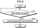
- FIG. 9 is a flowchart illustrating another initiation method according to a second modification of the embodiment.
- the CPU 12 determines whether or not an amount of accesses to the magnetic disk 24 from power-on of the magnetic disk device 1 or from previous execution of the signature check program 300 matches with a given threshold (S 601 ).
- the amount of writing or reading may be counted as the amount of accesses. Alternatively, the total amount of writing and reading may be counted.
- the amount of accesses may be represented by data size or the number of commands.
- the CPU 12 After determining that the amount of accesses does not match with the given threshold (No in S 601 ), the CPU 12 executes the operation of S 601 again. After determining that the amount of accesses matches with the given threshold (Yes in S 601 ), the CPU 12 initiates the signature check program 300 (S 602 ) and ends the operation.
- An example of the initiation of S 602 is similar to S 502 described with reference to FIG. 8 .
- the CPU 12 may execute the signature check program 300 every time a preset time period elapses.
- the CPU 12 may execute the signature check program 300 every time the amount of accesses to the magnetic disk 24 reaches a preset value.
- the processor upon satisfaction of a certain condition during execution of the first program, verifies the second program on the basis of the digital signature in the first memory and the public key in the second memory, in accordance with the third program. After finding a result of the verification as a pass, the processor analyzes the first program in the first memory in accordance with the second program in the first memory. The processor refrains from analyzing the first program in accordance with the second program, after finding the result of the verification as a fail. Thereby, the processor can securely analyze the first program.
Landscapes
- Engineering & Computer Science (AREA)
- Computer Security & Cryptography (AREA)
- Theoretical Computer Science (AREA)
- Computer Hardware Design (AREA)
- General Engineering & Computer Science (AREA)
- Software Systems (AREA)
- Signal Processing (AREA)
- Physics & Mathematics (AREA)
- General Physics & Mathematics (AREA)
- Computer Networks & Wireless Communication (AREA)
- Computing Systems (AREA)
- Health & Medical Sciences (AREA)
- Bioethics (AREA)
- General Health & Medical Sciences (AREA)
- Debugging And Monitoring (AREA)
- Storage Device Security (AREA)
- Signal Processing For Digital Recording And Reproducing (AREA)
Abstract
Description
Claims (17)
Applications Claiming Priority (2)
| Application Number | Priority Date | Filing Date | Title |
|---|---|---|---|
| JP2020040206A JP7249968B2 (en) | 2020-03-09 | 2020-03-09 | Information processing equipment and storage |
| JP2020-040206 | 2020-03-09 |
Publications (2)
| Publication Number | Publication Date |
|---|---|
| US20210281423A1 US20210281423A1 (en) | 2021-09-09 |
| US11888990B2 true US11888990B2 (en) | 2024-01-30 |
Family
ID=77556212
Family Applications (1)
| Application Number | Title | Priority Date | Filing Date |
|---|---|---|---|
| US17/002,968 Active 2041-12-09 US11888990B2 (en) | 2020-03-09 | 2020-08-26 | Information processing device controlling analysis of a program being executed based on a result of verification of an analysis program |
Country Status (2)
| Country | Link |
|---|---|
| US (1) | US11888990B2 (en) |
| JP (1) | JP7249968B2 (en) |
Families Citing this family (1)
| Publication number | Priority date | Publication date | Assignee | Title |
|---|---|---|---|---|
| JP7249968B2 (en) * | 2020-03-09 | 2023-03-31 | 株式会社東芝 | Information processing equipment and storage |
Citations (64)
| Publication number | Priority date | Publication date | Assignee | Title |
|---|---|---|---|---|
| US4912628A (en) * | 1988-03-15 | 1990-03-27 | International Business Machines Corp. | Suspending and resuming processing of tasks running in a virtual machine data processing system |
| US5063498A (en) * | 1986-03-27 | 1991-11-05 | Kabushiki Kaisha Toshiba | Data processing device with direct memory access function processed as an micro-code vectored interrupt |
| US5349680A (en) * | 1990-11-07 | 1994-09-20 | Kabushiki Kaisha Toshiba | Information processing apparatus for executing application programs under control of a system program |
| US5659759A (en) * | 1992-09-21 | 1997-08-19 | Kabushiki Kaisha Toshiba | Data processing device having improved interrupt controller to process interrupts of different priority levels |
| JPH10333939A (en) | 1997-05-28 | 1998-12-18 | Matsushita Electric Ind Co Ltd | Microprocessor |
| US6038631A (en) * | 1992-01-20 | 2000-03-14 | Kabushiki Kaisha Toshiba | Data processing system and method using virtual storage system |
| US6070220A (en) * | 1996-12-09 | 2000-05-30 | Kabushiki Kaisha Toshiba | Jump code generator, interrupt program selection system, interruption program selection method, and computer with the function |
| US20020027907A1 (en) * | 2000-08-21 | 2002-03-07 | Kabushiki Kaisha Toshiba | Packet transfer apparatus and method, and storage medium which stores program therefor |
| US20020144053A1 (en) * | 2001-03-30 | 2002-10-03 | Hitachi, Ltd. | Microcomputer, programming method and erasing method |
| US6553513B1 (en) * | 1999-02-19 | 2003-04-22 | Texas Instruments Incorporated | Emulation suspend mode with differing response to differing classes of interrupts |
| US20030172215A1 (en) * | 2000-12-16 | 2003-09-11 | Jorg Franke | Interrupt- controller |
| JP2004171416A (en) * | 2002-11-21 | 2004-06-17 | Ntt Docomo Inc | Communication terminal, value entity providing server, application distribution server, electronic purchase support system, electronic purchase support method, and electronic purchase support program |
| US6775778B1 (en) * | 1998-05-29 | 2004-08-10 | Texas Instruments Incorporated | Secure computing device having boot read only memory verification of program code |
| US20050132217A1 (en) * | 2003-02-07 | 2005-06-16 | Broadon Communications Corp. | Secure and backward-compatible processor and secure software execution thereon |
| US20050166069A1 (en) * | 2000-02-14 | 2005-07-28 | Kabushiki Kaisha Toshiba | Tamper resistant microprocessor |
| US20050273757A1 (en) * | 2004-06-07 | 2005-12-08 | Anderson Craig D | Methods, systems, and computer program products for summarizing operational behavior of a computer program |
| US7043641B1 (en) * | 2000-03-08 | 2006-05-09 | Igt | Encryption in a secure computerized gaming system |
| JP3873603B2 (en) * | 1999-10-22 | 2007-01-24 | 株式会社日立製作所 | Digital signature method and apparatus |
| JP2007066259A (en) * | 2005-09-02 | 2007-03-15 | Hitachi Ltd | Computer system, storage system, and volume capacity expansion method |
| JP2007183844A (en) * | 2006-01-10 | 2007-07-19 | Hitachi Global Storage Technologies Netherlands Bv | Auxiliary storage device and recording / reproducing method |
| US20080204920A1 (en) * | 2007-02-28 | 2008-08-28 | Kotaro Muramatsu | Storage device |
| JP2009009372A (en) | 2007-06-28 | 2009-01-15 | Panasonic Corp | Information terminal, client server system, and program |
| US20090199049A1 (en) * | 2008-02-01 | 2009-08-06 | Fujitsu Limited | Program processing device and program processing method |
| CN101606164A (en) * | 2007-02-09 | 2009-12-16 | 株式会社Ntt都科摩 | Terminal device and software inspection method |
| JP4447977B2 (en) | 2004-06-30 | 2010-04-07 | 富士通マイクロエレクトロニクス株式会社 | Secure processor and program for secure processor. |
| US20110188154A1 (en) * | 2010-01-29 | 2011-08-04 | Kabushiki Kaisha Toshiba | Magnetic disk device and control method thereof, and information processor |
| US20110213987A1 (en) * | 2010-02-26 | 2011-09-01 | Kabushiki Kaisha Toshiba | Controller for data storage device, data storage device, and control method thereof |
| JP4814993B2 (en) | 2007-03-27 | 2011-11-16 | 富士通株式会社 | Device to be debugged, authentication program, and debug authentication method |
| US20110292538A1 (en) * | 2010-05-31 | 2011-12-01 | Kabushiki Kaisha Toshiba | Recording medium controller and method thereof |
| US20110296204A1 (en) * | 2010-05-25 | 2011-12-01 | Via Technologies, Inc. | Microprocessor that facilitates task switching between encrypted and unencrypted programs |
| JP2011253610A (en) * | 2011-06-28 | 2011-12-15 | Toshiba Corp | Recorder and head projection amount control method |
| WO2012049750A1 (en) | 2010-10-14 | 2012-04-19 | トヨタ自動車 株式会社 | Vehicle data acquisition system and vehicle data acquisition method |
| US20120192170A1 (en) * | 2011-01-24 | 2012-07-26 | Sony Computer Entertainment Inc. | Information Processing Apparatus |
| JP5049288B2 (en) | 2006-11-09 | 2012-10-17 | パナソニック株式会社 | Tamper detection system, tamper detection method, tamper detection program, recording medium, integrated circuit, authentication information generation device, and tamper detection device |
| US20120300341A1 (en) * | 2011-05-24 | 2012-11-29 | Kabushiki Kaisha Toshiba | Information recorder and information recording method |
| TW201312575A (en) * | 2011-05-10 | 2013-03-16 | 電子戰協會公司 | System and method for implementing content verification of microcomputer-based circuits |
| JP2013069053A (en) * | 2011-09-21 | 2013-04-18 | Toshiba Corp | Control device and monitoring program |
| US20130124843A1 (en) * | 2011-11-04 | 2013-05-16 | Insyde Software Corp. | Secure boot administration in a unified extensible firmware interface (uefi)-compliant computing device |
| WO2013161974A1 (en) * | 2012-04-24 | 2013-10-31 | 大日本印刷株式会社 | Method for distributing and executing application program capable of detecting falsification |
| KR20140019402A (en) * | 2011-03-30 | 2014-02-14 | 이르데토 비.브이. | Establishing unique key during chip manufacturing |
| US20140123234A1 (en) * | 2012-10-31 | 2014-05-01 | Optim Corporation | User terminal, reliability management server, and method and program for preventing unauthorized remote operation |
| US20140258726A1 (en) * | 2013-03-08 | 2014-09-11 | Kabushiki Kaisha Toshiba | Smart card, electronic device, and portable electronic device |
| US20140298026A1 (en) * | 2013-03-26 | 2014-10-02 | Kabushiki Kaisha Toshiba | Information processing device and computer program product |
| US20150046717A1 (en) | 2013-08-12 | 2015-02-12 | Kabushiki Kaisha Toshiba | Semiconductor apparatus |
| KR20150045037A (en) * | 2013-10-17 | 2015-04-28 | 주식회사 씽크풀 | Method for application control and control system thereof |
| KR20150045053A (en) * | 2013-10-17 | 2015-04-28 | 주식회사 씽크풀 | Method for application control and control system thereof |
| KR20150099697A (en) * | 2015-08-11 | 2015-09-01 | 주식회사 씽크풀 | Method for application control and control system thereof |
| JP5796447B2 (en) * | 2011-10-07 | 2015-10-21 | 株式会社リコー | Information processing apparatus, validity verification method, validity verification program |
| US20160055331A1 (en) * | 2013-03-28 | 2016-02-25 | Irdeto B.V. | Detecting exploits against software applications |
| US9392017B2 (en) * | 2010-04-22 | 2016-07-12 | The Trustees Of Columbia University In The City Of New York | Methods, systems, and media for inhibiting attacks on embedded devices |
| US9454461B1 (en) * | 2015-04-15 | 2016-09-27 | International Business Machines Corporation | Call stack display with program flow indication |
| JP2017033248A (en) | 2015-07-31 | 2017-02-09 | パナソニックIpマネジメント株式会社 | Processing device, car onboard terminal device, method for activating processing device, and program for activating processing device |
| EP2975546B1 (en) * | 2014-07-16 | 2018-06-13 | General Electric Company | Systems and methods for verifying the authenticity of an application during execution |
| US20180165451A1 (en) * | 2015-06-16 | 2018-06-14 | Nec Corporation | Analysis system, analysis method, analysis device, and storage medium |
| JP2018195329A (en) | 2018-07-19 | 2018-12-06 | 株式会社東芝 | Information processing device |
| WO2019128673A1 (en) * | 2017-12-29 | 2019-07-04 | 华为技术有限公司 | Processing method, apparatus and device for flash disconnection of hard disk, and storage medium |
| KR102029045B1 (en) * | 2017-11-17 | 2019-10-07 | 주식회사 바이널익스피리언스 | Digial detox program for restricting usage of mobile terminal and calculating harmfulness score of application installed in mobile terminal, and digital detox service providing method |
| US20200104211A1 (en) * | 2018-09-28 | 2020-04-02 | Canon Kabushiki Kaisha | Information processing apparatus, and method of controlling the same |
| US20200134232A1 (en) * | 2018-10-31 | 2020-04-30 | Canon Kabushiki Kaisha | Information processing apparatus and control method thereof |
| KR20200063535A (en) * | 2018-11-28 | 2020-06-05 | 삼성전자주식회사 | Server and method for determining the integrity of the appliacion using thereof |
| JP2020095470A (en) * | 2018-12-12 | 2020-06-18 | キヤノン株式会社 | Information processing apparatus and control method thereof |
| JP2020181540A (en) * | 2019-04-26 | 2020-11-05 | キヤノン株式会社 | Information processing apparatus and data verification method |
| US11048778B2 (en) * | 2014-06-13 | 2021-06-29 | Artis Solutions Co., Ltd | Application program |
| US20210281423A1 (en) * | 2020-03-09 | 2021-09-09 | Kabushiki Kaisha Toshiba | Information processing device |
Family Cites Families (10)
| Publication number | Priority date | Publication date | Assignee | Title |
|---|---|---|---|---|
| JPH04213109A (en) * | 1990-12-07 | 1992-08-04 | Toshiba Corp | Magnetic disk controller |
| JPH06236299A (en) * | 1993-02-10 | 1994-08-23 | Hitachi Ltd | System monitoring method and monitoring device |
| JPH11175412A (en) * | 1997-12-12 | 1999-07-02 | Nec Corp | System for sampling state information in disk controller and machine readable recording medium for recording program |
| JP2003067222A (en) * | 2001-08-28 | 2003-03-07 | Hitachi Ltd | Business flow operation information acquisition method and business flow system |
| JP5346608B2 (en) * | 2009-02-06 | 2013-11-20 | Kddi株式会社 | Information processing apparatus and file verification system |
| JP5126447B1 (en) | 2012-08-31 | 2013-01-23 | 大日本印刷株式会社 | Application program execution method |
| JP6354438B2 (en) | 2014-08-08 | 2018-07-11 | 大日本印刷株式会社 | Information processing apparatus, information processing system, and processing program |
| CN104462965B (en) | 2014-11-14 | 2018-03-13 | 华为技术有限公司 | Application integrity verification method and the network equipment |
| US9612899B2 (en) * | 2015-03-04 | 2017-04-04 | International Business Machines Corporation | Collaborative collection of diagnostics data of software programs |
| JP7052396B2 (en) * | 2018-02-13 | 2022-04-12 | 日本電気株式会社 | Data collection server, data collection system, data collection method and data collection program |
-
2020
- 2020-03-09 JP JP2020040206A patent/JP7249968B2/en active Active
- 2020-08-26 US US17/002,968 patent/US11888990B2/en active Active
Patent Citations (70)
| Publication number | Priority date | Publication date | Assignee | Title |
|---|---|---|---|---|
| US5063498A (en) * | 1986-03-27 | 1991-11-05 | Kabushiki Kaisha Toshiba | Data processing device with direct memory access function processed as an micro-code vectored interrupt |
| US4912628A (en) * | 1988-03-15 | 1990-03-27 | International Business Machines Corp. | Suspending and resuming processing of tasks running in a virtual machine data processing system |
| US5349680A (en) * | 1990-11-07 | 1994-09-20 | Kabushiki Kaisha Toshiba | Information processing apparatus for executing application programs under control of a system program |
| US6038631A (en) * | 1992-01-20 | 2000-03-14 | Kabushiki Kaisha Toshiba | Data processing system and method using virtual storage system |
| US5659759A (en) * | 1992-09-21 | 1997-08-19 | Kabushiki Kaisha Toshiba | Data processing device having improved interrupt controller to process interrupts of different priority levels |
| US6070220A (en) * | 1996-12-09 | 2000-05-30 | Kabushiki Kaisha Toshiba | Jump code generator, interrupt program selection system, interruption program selection method, and computer with the function |
| US6158023A (en) | 1997-05-28 | 2000-12-05 | Matsushita Electric Industrial Co., Ltd. | Debug apparatus |
| JPH10333939A (en) | 1997-05-28 | 1998-12-18 | Matsushita Electric Ind Co Ltd | Microprocessor |
| US6775778B1 (en) * | 1998-05-29 | 2004-08-10 | Texas Instruments Incorporated | Secure computing device having boot read only memory verification of program code |
| US6553513B1 (en) * | 1999-02-19 | 2003-04-22 | Texas Instruments Incorporated | Emulation suspend mode with differing response to differing classes of interrupts |
| JP3873603B2 (en) * | 1999-10-22 | 2007-01-24 | 株式会社日立製作所 | Digital signature method and apparatus |
| US20050166069A1 (en) * | 2000-02-14 | 2005-07-28 | Kabushiki Kaisha Toshiba | Tamper resistant microprocessor |
| US7043641B1 (en) * | 2000-03-08 | 2006-05-09 | Igt | Encryption in a secure computerized gaming system |
| US20020027907A1 (en) * | 2000-08-21 | 2002-03-07 | Kabushiki Kaisha Toshiba | Packet transfer apparatus and method, and storage medium which stores program therefor |
| US20030172215A1 (en) * | 2000-12-16 | 2003-09-11 | Jorg Franke | Interrupt- controller |
| US20020144053A1 (en) * | 2001-03-30 | 2002-10-03 | Hitachi, Ltd. | Microcomputer, programming method and erasing method |
| JP2004171416A (en) * | 2002-11-21 | 2004-06-17 | Ntt Docomo Inc | Communication terminal, value entity providing server, application distribution server, electronic purchase support system, electronic purchase support method, and electronic purchase support program |
| US20050132217A1 (en) * | 2003-02-07 | 2005-06-16 | Broadon Communications Corp. | Secure and backward-compatible processor and secure software execution thereon |
| US20050273757A1 (en) * | 2004-06-07 | 2005-12-08 | Anderson Craig D | Methods, systems, and computer program products for summarizing operational behavior of a computer program |
| JP4447977B2 (en) | 2004-06-30 | 2010-04-07 | 富士通マイクロエレクトロニクス株式会社 | Secure processor and program for secure processor. |
| US7865733B2 (en) | 2004-06-30 | 2011-01-04 | Fujitsu Semiconductor Limited | Secure processor and a program for a secure processor |
| JP2007066259A (en) * | 2005-09-02 | 2007-03-15 | Hitachi Ltd | Computer system, storage system, and volume capacity expansion method |
| JP2007183844A (en) * | 2006-01-10 | 2007-07-19 | Hitachi Global Storage Technologies Netherlands Bv | Auxiliary storage device and recording / reproducing method |
| JP5049288B2 (en) | 2006-11-09 | 2012-10-17 | パナソニック株式会社 | Tamper detection system, tamper detection method, tamper detection program, recording medium, integrated circuit, authentication information generation device, and tamper detection device |
| US8453206B2 (en) | 2006-11-09 | 2013-05-28 | Panasonic Corporation | Detecting unauthorized tampering of a program |
| CN101606164A (en) * | 2007-02-09 | 2009-12-16 | 株式会社Ntt都科摩 | Terminal device and software inspection method |
| US20080204920A1 (en) * | 2007-02-28 | 2008-08-28 | Kotaro Muramatsu | Storage device |
| JP4814993B2 (en) | 2007-03-27 | 2011-11-16 | 富士通株式会社 | Device to be debugged, authentication program, and debug authentication method |
| JP2009009372A (en) | 2007-06-28 | 2009-01-15 | Panasonic Corp | Information terminal, client server system, and program |
| US20090199049A1 (en) * | 2008-02-01 | 2009-08-06 | Fujitsu Limited | Program processing device and program processing method |
| US20110188154A1 (en) * | 2010-01-29 | 2011-08-04 | Kabushiki Kaisha Toshiba | Magnetic disk device and control method thereof, and information processor |
| US20110213987A1 (en) * | 2010-02-26 | 2011-09-01 | Kabushiki Kaisha Toshiba | Controller for data storage device, data storage device, and control method thereof |
| US9392017B2 (en) * | 2010-04-22 | 2016-07-12 | The Trustees Of Columbia University In The City Of New York | Methods, systems, and media for inhibiting attacks on embedded devices |
| US20110296204A1 (en) * | 2010-05-25 | 2011-12-01 | Via Technologies, Inc. | Microprocessor that facilitates task switching between encrypted and unencrypted programs |
| US20110292538A1 (en) * | 2010-05-31 | 2011-12-01 | Kabushiki Kaisha Toshiba | Recording medium controller and method thereof |
| WO2012049750A1 (en) | 2010-10-14 | 2012-04-19 | トヨタ自動車 株式会社 | Vehicle data acquisition system and vehicle data acquisition method |
| US8880284B2 (en) | 2010-10-14 | 2014-11-04 | Toyota Jidosha Kabushiki Kaisha | Vehicle data acquisition system and vehicle data acquisition method |
| US20130190946A1 (en) | 2010-10-14 | 2013-07-25 | Toyota Jidosha Kabushiki Kaisha | Vehicle data acquisition system and vehicle data acquisition method |
| US20120192170A1 (en) * | 2011-01-24 | 2012-07-26 | Sony Computer Entertainment Inc. | Information Processing Apparatus |
| KR20140019402A (en) * | 2011-03-30 | 2014-02-14 | 이르데토 비.브이. | Establishing unique key during chip manufacturing |
| TW201312575A (en) * | 2011-05-10 | 2013-03-16 | 電子戰協會公司 | System and method for implementing content verification of microcomputer-based circuits |
| US20120300341A1 (en) * | 2011-05-24 | 2012-11-29 | Kabushiki Kaisha Toshiba | Information recorder and information recording method |
| JP2011253610A (en) * | 2011-06-28 | 2011-12-15 | Toshiba Corp | Recorder and head projection amount control method |
| JP2013069053A (en) * | 2011-09-21 | 2013-04-18 | Toshiba Corp | Control device and monitoring program |
| JP5796447B2 (en) * | 2011-10-07 | 2015-10-21 | 株式会社リコー | Information processing apparatus, validity verification method, validity verification program |
| US20130124843A1 (en) * | 2011-11-04 | 2013-05-16 | Insyde Software Corp. | Secure boot administration in a unified extensible firmware interface (uefi)-compliant computing device |
| WO2013161974A1 (en) * | 2012-04-24 | 2013-10-31 | 大日本印刷株式会社 | Method for distributing and executing application program capable of detecting falsification |
| US20140123234A1 (en) * | 2012-10-31 | 2014-05-01 | Optim Corporation | User terminal, reliability management server, and method and program for preventing unauthorized remote operation |
| US20140258726A1 (en) * | 2013-03-08 | 2014-09-11 | Kabushiki Kaisha Toshiba | Smart card, electronic device, and portable electronic device |
| US20140298026A1 (en) * | 2013-03-26 | 2014-10-02 | Kabushiki Kaisha Toshiba | Information processing device and computer program product |
| US20160055331A1 (en) * | 2013-03-28 | 2016-02-25 | Irdeto B.V. | Detecting exploits against software applications |
| JP2015036847A (en) | 2013-08-12 | 2015-02-23 | 株式会社東芝 | Semiconductor device |
| US20150046717A1 (en) | 2013-08-12 | 2015-02-12 | Kabushiki Kaisha Toshiba | Semiconductor apparatus |
| KR20150045053A (en) * | 2013-10-17 | 2015-04-28 | 주식회사 씽크풀 | Method for application control and control system thereof |
| KR20150045037A (en) * | 2013-10-17 | 2015-04-28 | 주식회사 씽크풀 | Method for application control and control system thereof |
| US11048778B2 (en) * | 2014-06-13 | 2021-06-29 | Artis Solutions Co., Ltd | Application program |
| EP2975546B1 (en) * | 2014-07-16 | 2018-06-13 | General Electric Company | Systems and methods for verifying the authenticity of an application during execution |
| US9454461B1 (en) * | 2015-04-15 | 2016-09-27 | International Business Machines Corporation | Call stack display with program flow indication |
| US20180165451A1 (en) * | 2015-06-16 | 2018-06-14 | Nec Corporation | Analysis system, analysis method, analysis device, and storage medium |
| JP2017033248A (en) | 2015-07-31 | 2017-02-09 | パナソニックIpマネジメント株式会社 | Processing device, car onboard terminal device, method for activating processing device, and program for activating processing device |
| KR20150099697A (en) * | 2015-08-11 | 2015-09-01 | 주식회사 씽크풀 | Method for application control and control system thereof |
| KR102029045B1 (en) * | 2017-11-17 | 2019-10-07 | 주식회사 바이널익스피리언스 | Digial detox program for restricting usage of mobile terminal and calculating harmfulness score of application installed in mobile terminal, and digital detox service providing method |
| WO2019128673A1 (en) * | 2017-12-29 | 2019-07-04 | 华为技术有限公司 | Processing method, apparatus and device for flash disconnection of hard disk, and storage medium |
| JP2018195329A (en) | 2018-07-19 | 2018-12-06 | 株式会社東芝 | Information processing device |
| US20200104211A1 (en) * | 2018-09-28 | 2020-04-02 | Canon Kabushiki Kaisha | Information processing apparatus, and method of controlling the same |
| US20200134232A1 (en) * | 2018-10-31 | 2020-04-30 | Canon Kabushiki Kaisha | Information processing apparatus and control method thereof |
| KR20200063535A (en) * | 2018-11-28 | 2020-06-05 | 삼성전자주식회사 | Server and method for determining the integrity of the appliacion using thereof |
| JP2020095470A (en) * | 2018-12-12 | 2020-06-18 | キヤノン株式会社 | Information processing apparatus and control method thereof |
| JP2020181540A (en) * | 2019-04-26 | 2020-11-05 | キヤノン株式会社 | Information processing apparatus and data verification method |
| US20210281423A1 (en) * | 2020-03-09 | 2021-09-09 | Kabushiki Kaisha Toshiba | Information processing device |
Non-Patent Citations (2)
| Title |
|---|
| Static Analysis of Runtime Errors in Interrupt-Driven Programs via Sequentialization by Xueguang Wu; Liqian Chen; Antoine Min'e; Wei Dong and Ji Wang pp. 26; Aug. 2016. * |
| U.S. Appl. No. 16/798,478; First Named Inventor: Yasuto Aramaki; Title: "Data Transfer Control Device, Data Transfer Control System, and Data Transfer Control Method", filed Feb. 24 2020. |
Also Published As
| Publication number | Publication date |
|---|---|
| US20210281423A1 (en) | 2021-09-09 |
| JP7249968B2 (en) | 2023-03-31 |
| JP2021140678A (en) | 2021-09-16 |
Similar Documents
| Publication | Publication Date | Title |
|---|---|---|
| US11455115B2 (en) | Storage device | |
| TWI471726B (en) | Managing cache data and metadata | |
| US10720225B2 (en) | Information processing apparatus, control method thereof, and storage mediumMD | |
| US20140149729A1 (en) | Reset vectors for boot instructions | |
| US8751817B2 (en) | Data processing apparatus and validity verification method | |
| US20120110343A1 (en) | Trustworthy timestamps on data storage devices | |
| US20170011769A1 (en) | Magnetic disk device and method of controlling magnetic disk device | |
| JP5466645B2 (en) | Storage device, information processing device, and program | |
| CN112558884B (en) | Data protection method and NVMe-based storage device | |
| CN112199740B (en) | Encryption lock implementation method and encryption lock | |
| US11645393B2 (en) | Secure booting in a data storage device with front end bus | |
| US9032540B2 (en) | Access system and method thereof | |
| US20100191944A1 (en) | Data storage apparatus | |
| US11888990B2 (en) | Information processing device controlling analysis of a program being executed based on a result of verification of an analysis program | |
| JPWO2010113282A1 (en) | Information processing apparatus having configuration change verification function and control method thereof | |
| CN102971984B (en) | Method for authenticating a storage device and host device | |
| CN102789430B (en) | Memory storage device, its memory controller and access method | |
| US20080244173A1 (en) | Storage device using nonvolatile cache memory and control method thereof | |
| JP2010165206A (en) | Memory controller and nonvolatile storage device | |
| CN101609492B (en) | Encryption and decryption method and system for embedded device | |
| CN103105783A (en) | Embedded device and control method thereof | |
| US8392759B2 (en) | Test method, test program, test apparatus, and test system | |
| CN119357979B (en) | Memory module and control method thereof, and electronic system | |
| CN116089327A (en) | Data protection method and related equipment | |
| TWI669608B (en) | Storage apparatus managing method and storage apparatus managing system |
Legal Events
| Date | Code | Title | Description |
|---|---|---|---|
| FEPP | Fee payment procedure |
Free format text: ENTITY STATUS SET TO UNDISCOUNTED (ORIGINAL EVENT CODE: BIG.); ENTITY STATUS OF PATENT OWNER: LARGE ENTITY |
|
| AS | Assignment |
Owner name: KABUSHIKI KAISHA TOSHIBA, JAPAN Free format text: ASSIGNMENT OF ASSIGNORS INTEREST;ASSIGNORS:ARAMAKI, YASUTO;YASUDA, SUSUMU;IWATA, TATSUAKI;SIGNING DATES FROM 20200917 TO 20201109;REEL/FRAME:054394/0670 |
|
| AS | Assignment |
Owner name: TOSHIBA ELECTRONIC DEVICES & STORAGE CORPORATION, JAPAN Free format text: CORRECTIVE ASSIGNMENT TO CORRECT THE RECEIVING PARTY DATA TO ADD THE SECOND ASSIGNEE'S NAME PREVIOUSLY RECORDED AT REEL: 054394 FRAME: 0670. ASSIGNOR(S) HEREBY CONFIRMS THE ASSIGNMENT;ASSIGNORS:ARAMAKI, YASUTO;YASUDA, SUSUMU;IWATA, TATSUAKI;SIGNING DATES FROM 20200917 TO 20201109;REEL/FRAME:054555/0127 Owner name: KABUSHIKI KAISHA TOSHIBA, JAPAN Free format text: CORRECTIVE ASSIGNMENT TO CORRECT THE RECEIVING PARTY DATA TO ADD THE SECOND ASSIGNEE'S NAME PREVIOUSLY RECORDED AT REEL: 054394 FRAME: 0670. ASSIGNOR(S) HEREBY CONFIRMS THE ASSIGNMENT;ASSIGNORS:ARAMAKI, YASUTO;YASUDA, SUSUMU;IWATA, TATSUAKI;SIGNING DATES FROM 20200917 TO 20201109;REEL/FRAME:054555/0127 |
|
| STPP | Information on status: patent application and granting procedure in general |
Free format text: NON FINAL ACTION MAILED |
|
| STPP | Information on status: patent application and granting procedure in general |
Free format text: FINAL REJECTION MAILED |
|
| STPP | Information on status: patent application and granting procedure in general |
Free format text: RESPONSE AFTER FINAL ACTION FORWARDED TO EXAMINER |
|
| STPP | Information on status: patent application and granting procedure in general |
Free format text: ADVISORY ACTION MAILED |
|
| STPP | Information on status: patent application and granting procedure in general |
Free format text: DOCKETED NEW CASE - READY FOR EXAMINATION |
|
| STPP | Information on status: patent application and granting procedure in general |
Free format text: NOTICE OF ALLOWANCE MAILED -- APPLICATION RECEIVED IN OFFICE OF PUBLICATIONS |
|
| STPP | Information on status: patent application and granting procedure in general |
Free format text: PUBLICATIONS -- ISSUE FEE PAYMENT RECEIVED |
|
| STPP | Information on status: patent application and granting procedure in general |
Free format text: PUBLICATIONS -- ISSUE FEE PAYMENT VERIFIED |
|
| STCF | Information on status: patent grant |
Free format text: PATENTED CASE |