US11876471B2 - Motor controller including resonant controllers - Google Patents
Motor controller including resonant controllers Download PDFInfo
- Publication number
- US11876471B2 US11876471B2 US17/358,147 US202117358147A US11876471B2 US 11876471 B2 US11876471 B2 US 11876471B2 US 202117358147 A US202117358147 A US 202117358147A US 11876471 B2 US11876471 B2 US 11876471B2
- Authority
- US
- United States
- Prior art keywords
- output
- motor
- component
- harmonic
- flux
- Prior art date
- Legal status (The legal status is an assumption and is not a legal conclusion. Google has not performed a legal analysis and makes no representation as to the accuracy of the status listed.)
- Active
Links
- 230000004907 flux Effects 0.000 claims description 54
- 238000000034 method Methods 0.000 claims description 24
- 238000012546 transfer Methods 0.000 claims description 6
- 238000010586 diagram Methods 0.000 description 13
- 239000004065 semiconductor Substances 0.000 description 9
- 230000006870 function Effects 0.000 description 8
- 239000003990 capacitor Substances 0.000 description 6
- 230000009466 transformation Effects 0.000 description 6
- 238000004519 manufacturing process Methods 0.000 description 4
- 238000004804 winding Methods 0.000 description 4
- 230000001939 inductive effect Effects 0.000 description 3
- 230000008569 process Effects 0.000 description 3
- 238000006243 chemical reaction Methods 0.000 description 2
- 238000012986 modification Methods 0.000 description 2
- 230000004048 modification Effects 0.000 description 2
- 230000000630 rising effect Effects 0.000 description 2
- 230000009471 action Effects 0.000 description 1
- 230000002238 attenuated effect Effects 0.000 description 1
- 239000000872 buffer Substances 0.000 description 1
- 230000008859 change Effects 0.000 description 1
- 238000010276 construction Methods 0.000 description 1
- 230000005669 field effect Effects 0.000 description 1
- 238000007667 floating Methods 0.000 description 1
- 230000005415 magnetization Effects 0.000 description 1
- 229910044991 metal oxide Inorganic materials 0.000 description 1
- 150000004706 metal oxides Chemical class 0.000 description 1
- 238000012545 processing Methods 0.000 description 1
- 230000009467 reduction Effects 0.000 description 1
- 238000005070 sampling Methods 0.000 description 1
- 229910052710 silicon Inorganic materials 0.000 description 1
- 239000010703 silicon Substances 0.000 description 1
- 238000006467 substitution reaction Methods 0.000 description 1
- 230000001360 synchronised effect Effects 0.000 description 1
Images


Classifications
-
- H—ELECTRICITY
- H02—GENERATION; CONVERSION OR DISTRIBUTION OF ELECTRIC POWER
- H02M—APPARATUS FOR CONVERSION BETWEEN AC AND AC, BETWEEN AC AND DC, OR BETWEEN DC AND DC, AND FOR USE WITH MAINS OR SIMILAR POWER SUPPLY SYSTEMS; CONVERSION OF DC OR AC INPUT POWER INTO SURGE OUTPUT POWER; CONTROL OR REGULATION THEREOF
- H02M7/00—Conversion of ac power input into dc power output; Conversion of dc power input into ac power output
- H02M7/42—Conversion of dc power input into ac power output without possibility of reversal
- H02M7/44—Conversion of dc power input into ac power output without possibility of reversal by static converters
- H02M7/48—Conversion of dc power input into ac power output without possibility of reversal by static converters using discharge tubes with control electrode or semiconductor devices with control electrode
- H02M7/53—Conversion of dc power input into ac power output without possibility of reversal by static converters using discharge tubes with control electrode or semiconductor devices with control electrode using devices of a triode or transistor type requiring continuous application of a control signal
- H02M7/537—Conversion of dc power input into ac power output without possibility of reversal by static converters using discharge tubes with control electrode or semiconductor devices with control electrode using devices of a triode or transistor type requiring continuous application of a control signal using semiconductor devices only, e.g. single switched pulse inverters
- H02M7/5387—Conversion of dc power input into ac power output without possibility of reversal by static converters using discharge tubes with control electrode or semiconductor devices with control electrode using devices of a triode or transistor type requiring continuous application of a control signal using semiconductor devices only, e.g. single switched pulse inverters in a bridge configuration
- H02M7/53871—Conversion of dc power input into ac power output without possibility of reversal by static converters using discharge tubes with control electrode or semiconductor devices with control electrode using devices of a triode or transistor type requiring continuous application of a control signal using semiconductor devices only, e.g. single switched pulse inverters in a bridge configuration with automatic control of output voltage or current
- H02M7/53875—Conversion of dc power input into ac power output without possibility of reversal by static converters using discharge tubes with control electrode or semiconductor devices with control electrode using devices of a triode or transistor type requiring continuous application of a control signal using semiconductor devices only, e.g. single switched pulse inverters in a bridge configuration with automatic control of output voltage or current with analogue control of three-phase output
- H02M7/53876—Conversion of dc power input into ac power output without possibility of reversal by static converters using discharge tubes with control electrode or semiconductor devices with control electrode using devices of a triode or transistor type requiring continuous application of a control signal using semiconductor devices only, e.g. single switched pulse inverters in a bridge configuration with automatic control of output voltage or current with analogue control of three-phase output based on synthesising a desired voltage vector via the selection of appropriate fundamental voltage vectors, and corresponding dwelling times
-
- H—ELECTRICITY
- H02—GENERATION; CONVERSION OR DISTRIBUTION OF ELECTRIC POWER
- H02P—CONTROL OR REGULATION OF ELECTRIC MOTORS, ELECTRIC GENERATORS OR DYNAMO-ELECTRIC CONVERTERS; CONTROLLING TRANSFORMERS, REACTORS OR CHOKE COILS
- H02P27/00—Arrangements or methods for the control of AC motors characterised by the kind of supply voltage
- H02P27/04—Arrangements or methods for the control of AC motors characterised by the kind of supply voltage using variable-frequency supply voltage, e.g. inverter or converter supply voltage
- H02P27/16—Arrangements or methods for the control of AC motors characterised by the kind of supply voltage using variable-frequency supply voltage, e.g. inverter or converter supply voltage using ac to ac converters without intermediate conversion to dc
-
- H—ELECTRICITY
- H02—GENERATION; CONVERSION OR DISTRIBUTION OF ELECTRIC POWER
- H02M—APPARATUS FOR CONVERSION BETWEEN AC AND AC, BETWEEN AC AND DC, OR BETWEEN DC AND DC, AND FOR USE WITH MAINS OR SIMILAR POWER SUPPLY SYSTEMS; CONVERSION OF DC OR AC INPUT POWER INTO SURGE OUTPUT POWER; CONTROL OR REGULATION THEREOF
- H02M1/00—Details of apparatus for conversion
- H02M1/12—Arrangements for reducing harmonics from ac input or output
- H02M1/126—Arrangements for reducing harmonics from ac input or output using passive filters
-
- H—ELECTRICITY
- H02—GENERATION; CONVERSION OR DISTRIBUTION OF ELECTRIC POWER
- H02M—APPARATUS FOR CONVERSION BETWEEN AC AND AC, BETWEEN AC AND DC, OR BETWEEN DC AND DC, AND FOR USE WITH MAINS OR SIMILAR POWER SUPPLY SYSTEMS; CONVERSION OF DC OR AC INPUT POWER INTO SURGE OUTPUT POWER; CONTROL OR REGULATION THEREOF
- H02M7/00—Conversion of ac power input into dc power output; Conversion of dc power input into ac power output
- H02M7/42—Conversion of dc power input into ac power output without possibility of reversal
- H02M7/44—Conversion of dc power input into ac power output without possibility of reversal by static converters
- H02M7/48—Conversion of dc power input into ac power output without possibility of reversal by static converters using discharge tubes with control electrode or semiconductor devices with control electrode
- H02M7/53—Conversion of dc power input into ac power output without possibility of reversal by static converters using discharge tubes with control electrode or semiconductor devices with control electrode using devices of a triode or transistor type requiring continuous application of a control signal
- H02M7/537—Conversion of dc power input into ac power output without possibility of reversal by static converters using discharge tubes with control electrode or semiconductor devices with control electrode using devices of a triode or transistor type requiring continuous application of a control signal using semiconductor devices only, e.g. single switched pulse inverters
- H02M7/539—Conversion of dc power input into ac power output without possibility of reversal by static converters using discharge tubes with control electrode or semiconductor devices with control electrode using devices of a triode or transistor type requiring continuous application of a control signal using semiconductor devices only, e.g. single switched pulse inverters with automatic control of output wave form or frequency
- H02M7/5395—Conversion of dc power input into ac power output without possibility of reversal by static converters using discharge tubes with control electrode or semiconductor devices with control electrode using devices of a triode or transistor type requiring continuous application of a control signal using semiconductor devices only, e.g. single switched pulse inverters with automatic control of output wave form or frequency by pulse-width modulation
-
- H—ELECTRICITY
- H02—GENERATION; CONVERSION OR DISTRIBUTION OF ELECTRIC POWER
- H02P—CONTROL OR REGULATION OF ELECTRIC MOTORS, ELECTRIC GENERATORS OR DYNAMO-ELECTRIC CONVERTERS; CONTROLLING TRANSFORMERS, REACTORS OR CHOKE COILS
- H02P21/00—Arrangements or methods for the control of electric machines by vector control, e.g. by control of field orientation
- H02P21/05—Arrangements or methods for the control of electric machines by vector control, e.g. by control of field orientation specially adapted for damping motor oscillations, e.g. for reducing hunting
-
- H—ELECTRICITY
- H02—GENERATION; CONVERSION OR DISTRIBUTION OF ELECTRIC POWER
- H02P—CONTROL OR REGULATION OF ELECTRIC MOTORS, ELECTRIC GENERATORS OR DYNAMO-ELECTRIC CONVERTERS; CONTROLLING TRANSFORMERS, REACTORS OR CHOKE COILS
- H02P27/00—Arrangements or methods for the control of AC motors characterised by the kind of supply voltage
- H02P27/04—Arrangements or methods for the control of AC motors characterised by the kind of supply voltage using variable-frequency supply voltage, e.g. inverter or converter supply voltage
- H02P27/06—Arrangements or methods for the control of AC motors characterised by the kind of supply voltage using variable-frequency supply voltage, e.g. inverter or converter supply voltage using dc to ac converters or inverters
- H02P27/08—Arrangements or methods for the control of AC motors characterised by the kind of supply voltage using variable-frequency supply voltage, e.g. inverter or converter supply voltage using dc to ac converters or inverters with pulse width modulation
- H02P27/14—Arrangements or methods for the control of AC motors characterised by the kind of supply voltage using variable-frequency supply voltage, e.g. inverter or converter supply voltage using dc to ac converters or inverters with pulse width modulation with three or more levels of voltage
-
- H—ELECTRICITY
- H02—GENERATION; CONVERSION OR DISTRIBUTION OF ELECTRIC POWER
- H02P—CONTROL OR REGULATION OF ELECTRIC MOTORS, ELECTRIC GENERATORS OR DYNAMO-ELECTRIC CONVERTERS; CONTROLLING TRANSFORMERS, REACTORS OR CHOKE COILS
- H02P29/00—Arrangements for regulating or controlling electric motors, appropriate for both AC and DC motors
- H02P29/50—Reduction of harmonics
Definitions
- a three-phase motor includes, for example, three pairs of stator windings.
- Three sinusoidal currents, one for each pair of stator windings, are generated by, for example, a DC-to-AC inverter.
- the three sinusoidal currents are 120 degrees out-of-phase with respect to each other. With reference to a first of the sinusoidal currents, a second current is 120 degrees out-of-phase, and a third current is 240 degrees out-of-phase with respect to the first of the sinusoidal currents.
- a motor controller integrated circuit includes a storage device containing software.
- the IC also includes a processor core coupled to the storage device.
- the processor core has an output adapted to be coupled to a motor.
- the processor core is configured to execute the software to implement a resonant controller at a frequency that is a harmonic of a speed of a motor.
- a motor controller integrated circuit includes a three-phase inverter operable to be coupled to a motor.
- the IC includes circuitry coupled to the three-phase inverter.
- the circuitry is configured to convert sense current signals from a motor to a signal in a rotating reference frame, to implements a resonant controller on the signal in the rotating reference frame, and to generate an output signal for control of the motor using an output from the resonant controller.
- a method for controlling a motor includes converting sense current signals from the motor to a rotational signal in a rotating reference frame and attenuating, by a resonant controller, a portion of the rotational signal at a harmonic of the speed of the motor. The method also includes generating an output signal for control of the motor using an output from the resonant controller.
- FIG. 1 is a block diagram of a motor and a system for controlling the motor in accordance with an example.
- FIG. 2 is a functional block diagram of a field-oriented control technique for controlling the motor in accordance with an example.
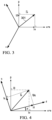
- FIG. 3 is a vector diagram illustrating the relationship between the time-domain motor sense currents and an orthogonal reference implemented by the Clarke transformation.
- FIG. 4 is a vector diagram illustrating the relationship between the orthogonal reference implemented by the Clarke transformation and a rotating reference frame implemented by the Park transformation.
- FIG. 5 is a waveform illustrating a sinusoidal back electromotive force (EMF).
- FIG. 6 is a waveform illustrating a back EMF with distortion.
- FIG. 7 is a circuit comprising one phase of a three-phase inverter in accordance with an example.
- FIGS. 8 and 9 are waveforms depicting gate voltages and switch node voltages of the circuit of FIG. 7 in accordance with various examples.
- FIGS. 10 and 11 are waveforms illustrating volt-seconds lost due to dead time implemented in the circuit of FIG. 7 .
- FIG. 12 is a functional block diagram of a field-oriented control technique for controlling the motor in accordance with another example.
- FIG. 13 is a flow chart depicting a method for controlling the motor in accordance with an example.
- FIG. 1 is a block diagram of a three-phase motor system 100 .
- the motor system 100 includes a processor core 110 , a storage device 120 , an input/output (I/O) interface 130 , an analog-to-digital converter (ADC) 150 , a three-phase inverter 140 , and a motor M.
- the processor core 110 is coupled to the storage device 120 and executes software 125 stored in the storage device 120 .
- Storage device 120 is a non-transitory storage device such as volatile memory (e.g., random access memory) or non-volatile memory (e.g., read-only memory), or combinations thereof. While a single processor core 110 is shown in FIG. 1 , other embodiments include multiple processor cores that collectively execute the software 125 .
- the processor core 110 implements the functionality described herein upon execution of software 125 .
- the motor M includes three phases a, b, and c, and each phase has a pair of stator windings that receives a sinusoidal, or approximately sinusoidal, current from the three-phase inverter 140 .
- Phases a, b, and c receive sinusoidal currents 154 , 155 , and 156 , respectively, from the three-phase inverter 140 .
- the I/O interface 130 and the ADC 150 also are coupled to the processor core 110 .
- the processor core 110 generates control signals on signal lines 115 that the I/O interface 130 outputs to the three-phase inverter 140 as signals ma, mb, and mc.
- the I/O interface 130 may include buffers to drive signals ma, mb, and mc to the three-phase inverter 140 .
- the three-phase inverter 140 includes a pair of transistor switches (a high side transistor coupled to a low side transistor at a switch node) for each of the three phases a, b, and c.
- Each of the signals ma, mb and mc from the processor core 110 is used by the inverter 140 to implement the duty cycle for the respective high side and low side transistors.
- the duty cycle for the high side transistor is 1+m/2, where m is the respective value of ma, mb, or mc.
- the duty cycle for the corresponding low side transistor is
- the ADC 150 receives analog signals Ia 151 , Ib 152 , and Ic 153 from current sensors 157 , 158 , and 159 , respectively.
- Analog signals Ia, Ib, and Ic represent (e.g., are directly proportional to) the instantaneous currents 154 , 155 , and 156 of the three phases a, b, and c, respectively.
- each of analog signals Ia, Ib and Ic is a voltage proportional to the instantaneous magnitude of its respective phase current 154 - 156 .
- the processor core 110 , storage device 120 , I/O interface 130 , and ADC 140 are fabricated on the same integrated circuit (IC) (e.g. on a single semiconductor die or multiple semiconductor dies that are interconnected within a IC package).
- the storage device 120 may be fabricated on an IC separate from the IC that includes the processor core 110 , I/O interface 130 , inverter 140 , and ADC 150 .
- any two or more of the processor core 110 , storage device 120 , I/O interface 130 , inverter 140 , and ADC 150 can be fabricated on the same IC.
- the three-phase inverter 140 may be implemented on the same semiconductor die as the other circuit elements or can be fabricated on a separate semiconductor die but incorporated into the same IC package/module as the other circuit structures.
- the processor core 110 upon execution of software 125 , implements a field-oriented control (FOC) technique for controlling the operation of motor M.
- FOC field-oriented control
- the FOC technique described below separately controls the torque and magnetic flux components of the motor's stator current.
- FIG. 2 is a functional block diagram 200 of the software 125 for implementing the FOC technique.
- the functional blocks included in FIG. 2 may be implemented using any combination of circuitry (e.g. processors, microprocessors, microcontrollers, state machines, ADC, DAC, flip-flops, registers, and/or logic circuits) and/or software.
- the block diagram of FIG. 2 includes a Clarke transform 210 , a Park transform 220 , an inverse Park transform 230 , and a space vector pulse width modulator (PWM) 240 .
- the space vector PWM 240 includes an inverse Clarke transform.
- the block diagram 200 further includes a speed and position estimator 260 , proportional integral (PI) controllers 271 , 272 , and 273 , and subtractors 281 , 282 , and 283 .
- the digital values from ADC 150 (ADC 150 is not shown in FIG. 2 ) corresponding to analog signals Ia, Ib, and Ic are provided as inputs to the Clarke transform 210 .
- two of the three analog signals Ia-Ic are used by the Clarke transform 210 , as explained below.
- Each of the current sensors 157 - 159 may be implemented as a sense resistor included within each of the inverter's three phases.
- the sense resistors may be coupled to a low side switch within the respective phase (shown in FIG. 7 , described below). Current flows through the sense resistor only when the respective low side switch is on. Because the low side switch and its high side switch counterpart are reciprocally turned on and off at a sinusoidally varying duty cycle (explained below), during a portion of each switching period, the low side switch is off. When the low side switch is off, no current flows through the sense resistor and thus that phase's sense current signal (Ia-Ic) is not available for use by the Clarke transform. Accordingly, two of the sense current signals are used by the Clarke transform, with the selection varying as to which two sense current signals are to be used at any point in time.
- phase's sense current signal Ia-Ic
- the Clarke transform 210 projects the three-phase system (Ia, Ib, Ic) into a two-dimensional ( ⁇ , ⁇ ) orthogonal system.
- the Clarke transform 210 implements the following equations to convert Ia and Ib to I ⁇ and I ⁇ .
- Currents Ia and Ib are assumed to be the two selected currents in Eq. (1), but in general, Eq. (1) uses any two of the three currents Ia, Ib and Ic.
- FIG. 3 shows the relationship between the three-phase a, b, c coordinate system and the two-dimensional ( ⁇ , ⁇ ) orthogonal system.
- Currents Ia-Ic are 120 degrees out of phase with respect to each other and are on the respective a-c axes in FIG. 3 .
- Current vector I ⁇ is in-line with the a-axis (the a and ⁇ -axes are colinear) and current vector I ⁇ is along the ⁇ -axis.
- the ⁇ -axis is orthogonal to the ⁇ -axis.
- Vector 301 is the complex stator current vector (Is) which is the vector sum of I ⁇ and I ⁇ and thus is a mathematical combination (per Eq. (1)) of the motor's current signals Ia and Ib.
- the Clarke transform 210 outputs I ⁇ and I ⁇ as inputs to the Park transform 220 .
- the Park transform 220 projects the ( ⁇ , ⁇ ) orthogonal system onto a rotating reference frame (d,q) as shown in FIG. 4 .
- the rotating reference frame is a reference frame that spins at a constant angular speed, which may or may not be same as the speed of the rotor.
- the speed of the rotating reference frame is the same as rotor speed and the d-axis of the rotating reference frame aligns with the d-axis of the rotor. Accordingly, the d-axis of the rotating reference frame is aligned with the rotor's flux.
- the angle ⁇ between the a-axis and the d-axis is the rotor flux position.
- the rotor flux position ⁇ is computed by the speed and position estimator 260 and is provided to the Park transform 220 .
- the q-axis is aligned with rotor torque.
- the Park transform 220 computes the flux (Id) and torque (Iq) components in the (d,q) domain as follows:
- the speed and position estimator 260 receives as inputs the outputs I ⁇ and I ⁇ from the Clarke transform 210 , as well as signals V ⁇ and V ⁇ which are output values from the inverse Park transform 230 . Using the values of I ⁇ , I ⁇ , V ⁇ , and V ⁇ , the speed and position estimator 260 computes the back electromotive force (EMF), and then using the computed back EMF, computes rotor speed w and flux position ⁇ . In one embodiment, the speed and position estimator 260 computes the back EMF in the ⁇ , ⁇ reference frame
- [ E ⁇ ⁇ E ⁇ ⁇ ] [ V ⁇ ⁇ V ⁇ ⁇ ] - ( rs * [ I ⁇ ⁇ I ⁇ ⁇ ] ) - d dt ⁇ ( [ L ⁇ ⁇ ⁇ ⁇ ⁇ L ⁇ ⁇ ⁇ ⁇ L ⁇ ⁇ ⁇ ⁇ L ⁇ ⁇ ⁇ ⁇ ] * [ I ⁇ ⁇ I ⁇ ⁇ ] ) ( 3 ) where rs is the motor's resistance and
- the speed and position estimator 260 then computes the back EMF in the d,q rotating reference frame based on the back EMF in the ⁇ , ⁇ reference frame and then computes rotor speed and flux position as provided in equations 4-6.
- the subtractor 281 subtracts the rotor speed w from a reference speed value ⁇ ref (the target speed for the motor and generated by the processor core 110 ) to produce an error value err ⁇ 289 .
- the error value err ⁇ 289 is an input to the PI controller 271 .
- the PI controllers 271 - 273 are control loop software modules that employ feedback. In general, a PI controller repeatedly receives an error value that is the difference between a desired setpoint (e.g., reference speed value ⁇ ref in the case of PI controller 271 ) and a measured process variable (e.g., rotor speed w), and generates an adjustment for another process variable based on proportional and integral terms.
- the generated adjustment is War which is applied to Iq by subtractor 282 to generate output value errq 285 .
- a PI controller includes a proportional component and an integral component. The proportional component operates on the present value of the error while the integral component operates on previous error values.
- the proportional component ensures that the steady state error becomes small, but generally cannot ensure the error to be zero. However, because it operates on present error values, the proportional component converges relatively quickly.
- the integral component ensures that steady state error becomes zero. However, because it operates on previous values of error (error history), it converges more slowly than the proportional component.
- the proportional component of a PI controller reduces the error to a relatively low value, and the integral component further reduces the error to zero.
- the speed at which the PI controller converges and any overshoot or undershoot observed are determined by the values of the proportional gain (Kp) and the integral gain (Ki).
- the outputs from the Park transform 220 , Id and Iq, are flux and torque current values, respectively, in the d,q rotating reference frame.
- the Iq component from the Park transform is subtracted from the Idref value by subtractor 282 to produce an error value errq 285 .
- the PI controller 272 processes the value errq to compute the voltage value Vq in the (d,q) rotating reference frame.
- Subtractor 283 subtracts Id from a flux reference value Idref to compute a flux error value errd 291 .
- PI controller 273 receives error value errd 291 and outputs a voltage value Vd.
- the voltages Vq and Vd are the q-axis and d-axis voltages, respectively, applied to the motor so that the q-axis and d-axis currents match their respective references.
- the inverse Park transform 230 transforms the rotating frame flux and torque values Vd and Vq, respectively, into the corresponding values of V ⁇ and V ⁇ in the ( ⁇ , ⁇ ) stationary orthogonal reference frame.
- the rotor flux position ⁇ from the speed and position estimator 260 is also provided to the inverse Park transform 230 .
- the values V ⁇ and V ⁇ are then provided to the space vector PWM 240 which uses the values V ⁇ and V ⁇ to produce the signals ma, mb, and mc that drive the three-phase inverter 140 .
- the inverter 140 converts the voltage reference values (ma, mb, mc) to duty cycles that control the on and off states of the transistors within the respective inverter phase such that the voltage on the phase's switch node applied to the motor has an average voltage that is approximately the same as the voltage reference value (ma, mb, mc).
- the relationship between ma-mc and the respective duty cycle is provided above.
- each of the three-phase currents 154 - 156 generated by the three-phase inverter 140 should be sinusoidal, in practice they may not be sinusoidal.
- One cause of a non-sinusoidal motor phase current is a non-sinusoidal back electromotive force (EMF).
- FIG. 5 shows a back-EMF waveform that is sinusoidal.
- FIG. 6 shows an example of a back EMF waveform that is not sinusoidal.
- the back EMF may be distorted (not sinusoidal) due to, for example, non-linearities in the motor M. Examples of motor non-linearities include windings that are not properly spaced, non-uniform magnetization of a magnet in the motor for a given pole, etc.
- FIG. 7 shows an example of one phase of the three-phase inverter in which a transistor M 1 is coupled to a transistor M 2 .
- transistors M 1 and M 2 are N-type metal-oxide semiconductor field-effect transistors (nMOS).
- nMOS N-type metal-oxide semiconductor field-effect transistors
- a sense resistor Rs e.g. a resistor with a small resistance, such as, 0.1 ohms
- the sense resistor Rs is an example of a current sensor 157 , 159 , and 159 , because the voltage across resistor Rs is proportional to the current through transistor M 2 , which also is the current from the motor through transistor M 2 during the negative half cycle (described below) of the motor current.
- the voltage across the sense resistor Rs is proportional to the sense current signal Ia-Ic. Accordingly, and as explained above, the sense current signal for a given phase is available only when that phase's low side transistor (M 2 ) is on.
- Voltage Vdc is applied across the series combination of transistors M 1 and M 2 .
- Switch node SW is the connection between the transistors M 1 and M 2 and is coupled to a respective phase (a, b, or c) of the motor M.
- the body diodes D 1 and D 2 for transistors M 1 and M 2 are shown as well.
- the anode of body diode D 1 is coupled to switch node SW and the cathode of body diode D 1 is coupled to +Vdc.
- the cathode of body diode D 2 is coupled to switch node SW and the anode of body diode D 2 is coupled to ⁇ Vdc.
- Voltage 747 is the midpoint voltage of the DC bus (Vdc).
- Voltage 747 is a voltage that is half-way between +Vdc and ⁇ Vdc.
- the other two phases are configured similarly, that is, a pair of transistors coupled to Vdc with the switch node SW coupled to a respective phase of the motor M.
- the gate signal to transistor M 1 is labeled G 1 and the gate signal to transistor M 2 is labeled G 2 .
- the gate signals G 1 and G 2 are generated by the inverter 140 based on the respective ma-mc signal from the space vector PWM 240 .
- the relationship between the duty cycles of the gate signals G 1 and G 2 for a given phase based on the corresponding “m” value (ma, mb, and mc) from the space vector PWM 240 is provided above.
- Logic (not shown) converts the values of ma-mc to gate signals G 1 and G 2 for the transistors M 1 and M 2 of the respective phases. When transistor M 1 is on, switch node SW is pulled up to voltage +Vdc.
- transistor M 2 When transistor M 2 is on, switch node SW is pulled down to voltage ⁇ Vdc.
- the gate signal G 1 turns on transistor M 1
- the gate signal G 2 turns off transistor M 2 .
- the gate signal G 1 turns off transistor M 1 . That is, only one of the transistors M 1 and M 2 are on at any point in time. Transistors M 1 and M 2 should not be turned on at the same time to avoid a shoot-through condition.
- FIG. 8 is a timing diagram showing the gate signals G 1 and G 2 .
- each gate signal toggles between a lower voltage level and a higher voltage level.
- the respective transistor transistor M 1 for gate signal G 1 , and transistor M 2 for gate signal G 2 ) is turned on, in this example, when its gate signal is at the higher voltage level.
- gate signal G 1 is turned on at rising edge 802 .
- gate signal G 2 is turned on at rising edge 804 .
- the voltage of the switch node SW is also shown in FIG. 8 .
- the switch node voltage toggles between +Vdc and ⁇ Vdc with the switch node voltage being at +Vdc when transistor M 1 is on and being at ⁇ Vdc when transistor M 2 is on.
- the time period that the switch node voltage is at +Vdc is T 1 and the time period that the switch node voltage is at ⁇ Vdc is T 2 .
- the duty cycle (D) is the percentage of time of each switching cycle that transistor M 1 is on.
- a 50% (0.5) duty cycle is illustrated in the example of FIG. 8 , and thus the T 1 equals T 2 .
- T 1 equals T 2 .
- T 1 will be different than T 2 . For example, for a duty cycle of 0.75, M 1 is on for three-fourths of the switching period TP. For a duty cycle of 0.25, M 1 is on for one-fourth of the switching period TP.
- the space vector PWM 240 can control the average voltage on switch node SW. Accordingly, an approximation of a sinusoidal voltage can be generated on the switch node SW by the space vector PWM 240 varying the duty cycle D in a sinusoidal manner. In this manner, the inverter 140 produces an approximately sinusoidal voltage and current for each phase of the three-phase motor M.
- An example of such a sinusoidal switch node voltage is shown in FIG. 7 as waveform 710 .
- the switch node voltage progresses through a series of sinusoidally changing voltages 711 along the waveform 710 .
- the space vector PWM 240 adjusts the duty cycle D to produce that particular voltage.
- the duty cycle must be greater than 0.5 and thus transistor M 1 will be on for a longer period of time that M 2 is on for each switching period.
- To produce a negative average switch node voltage (e.g., during negative half-cycle 715 ), the duty cycle must be smaller than 0.5 and thus transistor M 2 will be on for a longer period of time that M 1 is on for each switching period.
- FIG. 9 illustrates the dead time as the time period Tdead (not necessarily drawn to scale). During the dead time Tdead, neither transistor M 1 nor M 2 is on.
- FIG. 9 shows example waveforms for G 1 and G 2 for a target 50% duty cycle. G 1 and G 2 are active (high) for the same time period Ton.
- G 1 is on for slightly less than 50% of the switching period TP due to the inclusion of deadtime.
- non-ideal switching of transistors M 1 and M 2 may cause or may be caused by non-instantaneous switching from low to high or high to low for the signals at the gates of transistor M 1 and M 2 .
- FIG. 9 illustrates two waveforms for the switch node voltage.
- Waveform 910 illustrates the switch node voltage during the positive half-cycle 715 of the sinusoidal phase current
- waveform 930 illustrates the switch node voltage during the negative half-cycle 716 of the sinusoidal phase current.
- the duty cycle should be greater than 50% for the positive half-cycle and less than 50% for the negative half-cycle, switch node waveforms 910 and 930 are shown for a target 50% duty cycle for simplicity.
- the switch node voltage is pulled down to ⁇ Vdc, as illustrated at 902 .
- deadtime 901 due to the inductive load of the motor, current continues to flow through the body diode D 2 in the direction of arrows 703 and 701 to the motor M thereby continuing to hold the switch node voltage at ⁇ Vdc.
- the switch node voltage is pulled up to +Vdc as shown at 906 , and during the ensuing dead time 907 , the current flows through body diode D 2 (due to the inductive load of the motor) holding the switch node voltage SW at ⁇ Vdc.
- the resulting waveform 910 for the switch node voltage during the positive half-cycle has a width of T 3 when the switch node voltage is at +Vdc and has a width of T 4 when the switch node voltage is at ⁇ Vdc.
- T 3 is less than 50% of the switching period TP (and smaller than T 4 ) due to the inclusion of the dead time.
- the average voltage on the switch node is smaller compared to the switch node voltage absent any dead time by a voltage that is Vdc*deadtime/TP, where “deadtime” is the amount of dead time in each switching period and TP is the switching period. For example, if the amount of dead time is 5% of TP, then average switch node voltage will be reduced by 5% compared to the switch node voltage absent any dead time.
- Waveform 930 shows the switch node voltage during the negative half-cycle 716 (when phase current flows in the direction of arrow 702 ).
- the switch node voltage is pulled up to +Vdc, as illustrated at 926 in waveform 930 .
- current continues to flow through the body diode D 1 in the direction of arrows 704 and 702 from the motor M thereby continuing to hold the switch node voltage at +Vdc.
- transistor M 2 is on (the gate signal G 2 is high)
- the switch node voltage is pulled down to ⁇ Vdc as shown at 927 .
- the current flows through body diode D 1 forcing the switch node voltage SW to +Vdc.
- the resulting waveform 930 for the switch node voltage during the negative half-cycle has a width of T 5 when the switch node voltage is at +Vdc and has a width of T 6 when the switch node voltage is at ⁇ Vdc.
- T 5 is larger than 50% (and larger than T 6 ) due to the inclusion of the dead time.
- the resulting average voltage on the switch node is less negative than the average voltage would have been absent the deadtime.
- the width of the positive pulses of the switch node voltage is different between the positive and negative half-cycles for the same duty cycle.
- the modulation of the duty cycle of the switch node voltage due to the inclusion of dead time results in a distortion to the phase currents provided to the motor M.
- Waveform 1001 is the sinusoidal current (i.e., absent any dead time) to one of the three phases of the motor M.
- Waveform 1002 is a square wave that represents the average volt-seconds lost. As explained above, dead time is included within each switching cycle during which neither transistor is on. The inclusion of dead time impacts the average voltage on the switch node. The average volt-seconds lost refers to the average reduction in voltage on the switch node due to the dead time and is positive during the positive half-cycle of the phase current and is negative during the negative half-cycle of the phase current as shown. Waveform 1002 is in-phase with the phase current.
- the phase current applied to the motor is the sinusoidal current (waveform 1001 ) minus the average volt-seconds lost (waveform 1002 ).
- the applied current thus has distortion at higher order harmonics due to the volt-seconds lost which results from the inclusion of dead time in each switching period.
- FIG. 11 also repeats the ideal sinusoidal phase current 1001 .
- Waveform 1102 is the superposition of the average volt-seconds lost square wave from each of the three phases. As the phase currents are 120 degrees phase shifted from each other, the volt-seconds lost square waves also are phase shifted from each other 120 degrees.
- the dominant harmonics of the resulting waveform 1102 are the fifth and seventh harmonics. Accordingly, analog signals Ia, Ib, and Ic have dominant harmonics at the fifth and seventh harmonics. However, after performance of the Clarke transform 210 and the Park transform 220 , the dominant harmonic of the flux component Id and the torque component Iq in the (d,q) domain is at the sixth harmonic.
- FIG. 12 is a functional block diagram 1200 of another implementation for the software 125 for implementing an FOC technique that attenuates the signal magnitude at the sixth harmonic in the (d,q) domain.
- FIG. 12 includes proportional resonant (PR) controllers 1210 and 1220 for torque and flux control, respectively.
- PR controller has a high gain (e.g. theoretically infinite) at a particular frequency, ⁇ 0, and a low gain (e.g., 0) at frequencies below and above ⁇ 0. Any signal amplitude at frequency ⁇ 0 is substantially attenuated by the PR controller.
- a continuous time domain transfer function for a PR controller is given in Eq. (9):
- y r K ⁇ r * s s 2 + ⁇ ⁇ 0 2 ( 9 )
- y is the output
- r is in the input
- Kr is resonant controller's gain
- s is the Laplace variable.
- the transfer function of Eq. (9) can be discretized using a bilinear transform with frequency pre-warping.
- the following expression is substituted for the Laplace variable “s” in the PR controller's transfer function of Eq. (9);
- y k r ⁇ T ⁇ s 2 ⁇ ( r - r - 2 ) + 2 ⁇ ⁇ 1 - ( tan ⁇ ( ⁇ ⁇ 0 * T ⁇ s 2 ) ) 2 ⁇ * ( y - 1 ) - ( 1 + ( tan ⁇ ( ⁇ ⁇ 0 * T ⁇ s 2 ) ) 2 ) ⁇ ( y - 2 ) 1 + ( tan ⁇ ( ⁇ ⁇ 0 * T ⁇ s 2 ) ) 2 ( 11 )
- r is the present input sample
- r ⁇ 2 is the input sample that is two samples preceding the present input sample
- y is the present output value
- y ⁇ 2 is the output sample immediately preceding the present output sample y ⁇ 1 .
- the software block diagram of FIG. 12 includes many of the same functional elements as in FIG. 2 , but also includes the PR controllers 1210 and 1220 and additional subtractors 1205 , 1212 , 1215 , and 1222 .
- the value Iq is provided to an inverting ( ⁇ ) input subtractor 1205 and a reference signal of 0 is provided to a non-inverting (+) input of subtractor 1205 .
- Subtractor 1205 computes an error signal 1206 which is provided to an input of PR controller 1210 .
- the output signal values 1211 from PR controller 1210 are added to the output values from PI 272 to produce a torque value Mq_ref 1213 to the inverse Park transform 230 .
- the PR controller 1210 is programmed for an ⁇ 0 in Eq (11) equal to the frequency of the sixth harmonic of the (d,q) domain current values.
- the sixth harmonic frequency is six-times the rotor speed w of the motor. For example, for a rotor speed of 50 radians per second, the sixth harmonic is a frequency of 300 radians per second.
- the rotor speed w is provided to the PR controllers 1210 and 1220 , and each PR controller computes the magnitude of the sixth harmonic for use in equation 11 above (as the value ⁇ 0).
- the speed and position estimator 260 computes the magnitude of the sixth harmonic and provides ⁇ 0 to the PR controllers 1210 and 1220 .
- the value Id is provided to an inverting input of subtractor 1215 and a reference value of 0 is provided to the non-inverting input of the subtractor 1215 .
- the error value 1216 is provided to an input of PR controller 1220 .
- the output values 1221 from PR controller 1220 are added to the output values from PI 273 to produce a flux value Md ref 1223 to the inverse Park transform 230 .
- the PR controller 1220 also is programmed for an ⁇ 0 in Eq (6) equal to the frequency of the sixth harmonic of (d,q) domain current values.
- the magnitude of the sixth harmonic in the DQ domain is reduced or eliminated. Consequently, through the conversion back to the three phase currents to the motor M through the inverse Park transform 230 and the space vector PWM 240 , the magnitude of the fifth and seventh harmonics in the phase currents 154 - 156 provided to the motor M are reduced resulting in phase currents with smaller fifth and seventh harmonic contributions. Accordingly, the resulting phase currents to the motor M are closer to true sinewaves than would have been the case without the use of the PR controllers 1210 and 1220 .
- FIG. 13 is a flow chart of an example method 1100 .
- the method includes converting ( 1301 ) sense current signals from the motor to a signal in a rotating reference frame.
- this conversion is performed by, for example, performance of a Clarke transformation and a Park transformation as described above.
- the output signals from the Park transformation are in the rotating reference frame, and represent flux and torque signals.
- the method further includes implementing first and second resonant controllers on respective flux and torque signals in the rotating reference frame.
- the resonant controllers are implemented at the sixth harmonic of the motor's speed.
- the method includes generating output signals for control of the motor using an output from the resonant controllers.
- the term “couple” may cover connections, communications, or signal paths that enable a functional relationship consistent with this description. For example, if device A generates a signal to control device B to perform an action: (a) in a first example, device A is coupled to device B by direct connection; or (b) in a second example, device A is coupled to device B through intervening component C if intervening component C does not alter the functional relationship between device A and device B, such that device B is controlled by device A via the control signal generated by device A.
- a device that is “configured to” perform a task or function may be configured (e.g., programmed and/or hardwired) at a time of manufacturing by a manufacturer to perform the function and/or may be configurable (or re-configurable) by a user after manufacturing to perform the function and/or other additional or alternative functions.
- the configuring may be through firmware and/or software programming of the device, through a construction and/or layout of hardware components and interconnections of the device, or a combination thereof.
- references to software functions or functional block diagrams may be implemented by software running on a processor, microcontroller or other type of processing device in conjunction with memory, in some example embodiments, or may be implemented using hardware (such as logic gates, processors, application specific integrated circuits, field programmable gate array and/or state machines), alone.
- terminal As used herein, the terms “terminal”, “node”, “interconnection”, “pin” and “lead” are used interchangeably. Unless specifically stated to the contrary, these terms are generally used to mean an interconnection between or a terminus of a device element, a circuit element, an integrated circuit, a device or other electronics or semiconductor component.
- a circuit or device that is described herein as including certain components may instead be adapted to be coupled to those components to form the described circuitry or device.
- a structure described as including one or more semiconductor elements such as transistors), one or more passive elements (such as resistors, capacitors, and/or inductors), and/or one or more sources (such as voltage and/or current sources) may instead include only the semiconductor elements within a single physical device (e.g., a semiconductor die and/or integrated circuit (IC) package) and may be adapted to be coupled to at least some of the passive elements and/or the sources to form the described structure either at a time of manufacture or after a time of manufacture, for example, by an end-user and/or a third-party.
- semiconductor elements such as transistors
- passive elements such as resistors, capacitors, and/or inductors
- sources such as voltage and/or current sources
- MOSFET metal-oxide-silicon FET
- BJTs bipolar junction transistors
- Circuits described herein are reconfigurable to include the replaced components to provide functionality at least partially similar to functionality available prior to the component replacement.
- Components shown as resistors are generally representative of any one or more elements coupled in series and/or parallel to provide an amount of impedance represented by the shown resistor.
- a resistor or capacitor shown and described herein as a single component may instead be multiple resistors or capacitors, respectively, coupled in parallel between the same nodes.
- a resistor or capacitor shown and described herein as a single component may instead be multiple resistors or capacitors, respectively, coupled in series between the same two nodes as the single resistor or capacitor.
- ground in the foregoing description include a chassis ground, an Earth ground, a floating ground, a virtual ground, a digital ground, a common ground, and/or any other form of ground connection applicable to, or suitable for, the teachings of this description. Unless otherwise stated, “about,” “approximately,” or “substantially” preceding a value means+/ ⁇ 10 percent of the stated value. Modifications are possible in the described examples, and other examples are possible within the scope of the claims.
Abstract
Description
The values of m (and thus the duty cycle values) are varied sinusoidally by the
The flux component id and the torque component iq are the outputs of the Park transform 220 and depend on the current vector components (Iα, Iβ) and on the rotor flux position θ. Per the FOC control technique,
using the following equation:
where rs is the motor's resistance and
The speed and position estimator computes rotor position θ, but the preceding equation for computing
uses rotor position θ. The assumption is that the motor's inductance does not appreciably change very quickly (e.g., within one sampling instance) and thus the rotor position θ previously computed by the speed and
The inductance value
where Ld and Lq are the d- and q-axis inductances, respectively. In one embodiment, the speed and
u(t)=Kp+Ki/s (7)
where u(t) is the ratio of the output value to the input value (e.g., an error value) from a PI controller, Kp is a proportional gain, Ki is an integral gain, s is the Laplace variable. A PI controller includes a proportional component and an integral component. The proportional component operates on the present value of the error while the integral component operates on previous error values. The proportional component ensures that the steady state error becomes small, but generally cannot ensure the error to be zero. However, because it operates on present error values, the proportional component converges relatively quickly. The integral component ensures that steady state error becomes zero. However, because it operates on previous values of error (error history), it converges more slowly than the proportional component. In general, the proportional component of a PI controller reduces the error to a relatively low value, and the integral component further reduces the error to zero. The speed at which the PI controller converges and any overshoot or undershoot observed are determined by the values of the proportional gain (Kp) and the integral gain (Ki).
Vα=Vd*cos(θ)−Vq*sin(θ)
Vβ=Vd*sin(θ)+V q*cos(θ) (8)
The values Vα and Vβ are then provided to the
where y is the output, r is in the input and Kr is resonant controller's gain, and s is the Laplace variable. To implement a PR controller in software, the transfer function of Eq. (9) can be discretized using a bilinear transform with frequency pre-warping. In accordance with a bilinear transform with frequency pre-warping, the following expression is substituted for the Laplace variable “s” in the PR controller's transfer function of Eq. (9);
In making this substitution, the implementation of the discretized resonant controller in
where r is the present input sample, r−2 is the input sample that is two samples preceding the present input sample, y is the present output value, is the output sample immediately preceding the present output sample y, and y−2 is the output sample immediately preceding y−1.
Claims (20)
Priority Applications (4)
| Application Number | Priority Date | Filing Date | Title |
|---|---|---|---|
| US17/358,147 US11876471B2 (en) | 2021-06-25 | 2021-06-25 | Motor controller including resonant controllers |
| DE112022003250.2T DE112022003250T5 (en) | 2021-06-25 | 2022-06-27 | ENGINE CONTROL WITH RESONANCE CONTROLS |
| CN202280041910.7A CN117480723A (en) | 2021-06-25 | 2022-06-27 | Motor controller including resonant controller |
| PCT/US2022/035051 WO2022272158A1 (en) | 2021-06-25 | 2022-06-27 | Motor controller including resonant controllers |
Applications Claiming Priority (1)
| Application Number | Priority Date | Filing Date | Title |
|---|---|---|---|
| US17/358,147 US11876471B2 (en) | 2021-06-25 | 2021-06-25 | Motor controller including resonant controllers |
Publications (2)
| Publication Number | Publication Date |
|---|---|
| US20220416713A1 US20220416713A1 (en) | 2022-12-29 |
| US11876471B2 true US11876471B2 (en) | 2024-01-16 |
Family
ID=84541684
Family Applications (1)
| Application Number | Title | Priority Date | Filing Date |
|---|---|---|---|
| US17/358,147 Active US11876471B2 (en) | 2021-06-25 | 2021-06-25 | Motor controller including resonant controllers |
Country Status (4)
| Country | Link |
|---|---|
| US (1) | US11876471B2 (en) |
| CN (1) | CN117480723A (en) |
| DE (1) | DE112022003250T5 (en) |
| WO (1) | WO2022272158A1 (en) |
Families Citing this family (1)
| Publication number | Priority date | Publication date | Assignee | Title |
|---|---|---|---|---|
| WO2020100225A1 (en) * | 2018-11-14 | 2020-05-22 | 東芝三菱電機産業システム株式会社 | Power conversion device |
Citations (11)
| Publication number | Priority date | Publication date | Assignee | Title |
|---|---|---|---|---|
| US6710495B2 (en) * | 2001-10-01 | 2004-03-23 | Wisconsin Alumni Research Foundation | Multi-phase electric motor with third harmonic current injection |
| US20070052381A1 (en) * | 2003-10-07 | 2007-03-08 | Jtekt Corporation | Electric power steering system |
| US20090237014A1 (en) * | 2007-05-24 | 2009-09-24 | Aisin Seiki Kabushiki Kaisha | Synchronous motor control device and method for optimizing synchronous motor control |
| US7768220B2 (en) * | 2008-04-24 | 2010-08-03 | Gm Global Technology Operations, Inc. | Harmonic torque ripple reduction at low motor speeds |
| US7986117B2 (en) * | 2008-03-21 | 2011-07-26 | Denso Corporation | Apparatus for carrying out improved control of rotary machine |
| US20110298405A1 (en) * | 2010-06-04 | 2011-12-08 | Stmicroelectronics S.R.L. | Method of controlling a three-phase permanent magnet synchronous motor for reducing acoustic noise and relative control device |
| US20140021894A1 (en) | 2012-07-19 | 2014-01-23 | GM Global Technology Operations LLC | Torque ripple reduction of multiple harmonic components |
| KR101405237B1 (en) | 2013-06-25 | 2014-06-10 | 현대자동차 주식회사 | System for controlling motor of eco-friendly car |
| US20150365038A1 (en) * | 2013-03-29 | 2015-12-17 | Aisin Aw Co., Ltd. | Rotary Electric Machine Driving Device |
| US20180234043A1 (en) | 2017-02-14 | 2018-08-16 | KSR IP Holdings, LLC | Alternator with harmonic compensation |
| JP2020156223A (en) | 2019-03-20 | 2020-09-24 | トヨタ自動車株式会社 | Driving device |
-
2021
- 2021-06-25 US US17/358,147 patent/US11876471B2/en active Active
-
2022
- 2022-06-27 DE DE112022003250.2T patent/DE112022003250T5/en active Pending
- 2022-06-27 WO PCT/US2022/035051 patent/WO2022272158A1/en active Application Filing
- 2022-06-27 CN CN202280041910.7A patent/CN117480723A/en active Pending
Patent Citations (11)
| Publication number | Priority date | Publication date | Assignee | Title |
|---|---|---|---|---|
| US6710495B2 (en) * | 2001-10-01 | 2004-03-23 | Wisconsin Alumni Research Foundation | Multi-phase electric motor with third harmonic current injection |
| US20070052381A1 (en) * | 2003-10-07 | 2007-03-08 | Jtekt Corporation | Electric power steering system |
| US20090237014A1 (en) * | 2007-05-24 | 2009-09-24 | Aisin Seiki Kabushiki Kaisha | Synchronous motor control device and method for optimizing synchronous motor control |
| US7986117B2 (en) * | 2008-03-21 | 2011-07-26 | Denso Corporation | Apparatus for carrying out improved control of rotary machine |
| US7768220B2 (en) * | 2008-04-24 | 2010-08-03 | Gm Global Technology Operations, Inc. | Harmonic torque ripple reduction at low motor speeds |
| US20110298405A1 (en) * | 2010-06-04 | 2011-12-08 | Stmicroelectronics S.R.L. | Method of controlling a three-phase permanent magnet synchronous motor for reducing acoustic noise and relative control device |
| US20140021894A1 (en) | 2012-07-19 | 2014-01-23 | GM Global Technology Operations LLC | Torque ripple reduction of multiple harmonic components |
| US20150365038A1 (en) * | 2013-03-29 | 2015-12-17 | Aisin Aw Co., Ltd. | Rotary Electric Machine Driving Device |
| KR101405237B1 (en) | 2013-06-25 | 2014-06-10 | 현대자동차 주식회사 | System for controlling motor of eco-friendly car |
| US20180234043A1 (en) | 2017-02-14 | 2018-08-16 | KSR IP Holdings, LLC | Alternator with harmonic compensation |
| JP2020156223A (en) | 2019-03-20 | 2020-09-24 | トヨタ自動車株式会社 | Driving device |
Non-Patent Citations (1)
| Title |
|---|
| International Search Report in corresponding PCT Application No. PCT/US2022/035051, dated Oct. 21, 2022 (3 pages). |
Also Published As
| Publication number | Publication date |
|---|---|
| US20220416713A1 (en) | 2022-12-29 |
| CN117480723A (en) | 2024-01-30 |
| WO2022272158A1 (en) | 2022-12-29 |
| DE112022003250T5 (en) | 2024-04-11 |
Similar Documents
| Publication | Publication Date | Title |
|---|---|---|
| US8674638B2 (en) | Determining initial rotor position of an alternating current motor | |
| Ren et al. | Direct torque control of permanent-magnet synchronous machine drives with a simple duty ratio regulator | |
| US6429620B2 (en) | Motor control device | |
| US7642737B2 (en) | Anti-windup control for a current regulator of a pulse width modulation inverter | |
| US8395339B2 (en) | Motor control device | |
| KR20140133783A (en) | Optimized control for synchronous motors | |
| US20160248354A1 (en) | Rotor position estimation apparatus and methods | |
| US10044310B2 (en) | Methods of auto tuning machine parameters and systems thereof | |
| Hoshino et al. | Output voltage correction for a voltage source type inverter of an induction motor drive | |
| US11876471B2 (en) | Motor controller including resonant controllers | |
| JP4722002B2 (en) | PWM inverter control device, PWM inverter control method, and refrigeration air conditioner | |
| US11764710B2 (en) | Automatic transition of motor controller from open-loop control to closed-loop control | |
| Tang et al. | Compensation of dead-time effects based on revised repetitive controller for PMSM drives | |
| JP6372424B2 (en) | Power converter and current detection method | |
| JP2004135441A (en) | Motor driving method and its device | |
| EP3958457A1 (en) | Electric motor control device | |
| US20230188066A1 (en) | Predictive deadbeat control of motor phase currents with model mismatch compensation and adjustable control dynamics | |
| US11139765B1 (en) | Dynamic decoupling control with active noise cancellation | |
| Yoon et al. | New flux weakening control for surface mounted permanent magnet synchronous machine using gradient descent method | |
| Qiu et al. | Flux observer with two-phase-type PLL for sensorless direct torque control of surface mounted PMSM drives | |
| US20240007035A1 (en) | Open-loop motor control | |
| Saleh et al. | Frame-angle-based direct torque controller for PMSM drives | |
| Lakaparampil et al. | Design, modelling, simulation and implementation of vector controlled induction motor drive | |
| Lazi et al. | Sensorless speed control of PMSM drives using dSPACE DS1103 board | |
| US20220131488A1 (en) | Controller for ac rotary electric machine |
Legal Events
| Date | Code | Title | Description |
|---|---|---|---|
| AS | Assignment |
Owner name: TEXAS INSTRUMENTS INCORPORATED, TEXAS Free format text: ASSIGNMENT OF ASSIGNORS INTEREST;ASSIGNOR:KULKARNI, PRASAD;REEL/FRAME:056665/0331 Effective date: 20210625 |
|
| FEPP | Fee payment procedure |
Free format text: ENTITY STATUS SET TO UNDISCOUNTED (ORIGINAL EVENT CODE: BIG.); ENTITY STATUS OF PATENT OWNER: LARGE ENTITY |
|
| STPP | Information on status: patent application and granting procedure in general |
Free format text: RESPONSE TO NON-FINAL OFFICE ACTION ENTERED AND FORWARDED TO EXAMINER |
|
| STPP | Information on status: patent application and granting procedure in general |
Free format text: FINAL REJECTION MAILED |
|
| STPP | Information on status: patent application and granting procedure in general |
Free format text: RESPONSE AFTER FINAL ACTION FORWARDED TO EXAMINER |
|
| STPP | Information on status: patent application and granting procedure in general |
Free format text: NOTICE OF ALLOWANCE MAILED -- APPLICATION RECEIVED IN OFFICE OF PUBLICATIONS |
|
| STPP | Information on status: patent application and granting procedure in general |
Free format text: PUBLICATIONS -- ISSUE FEE PAYMENT RECEIVED |
|
| STPP | Information on status: patent application and granting procedure in general |
Free format text: PUBLICATIONS -- ISSUE FEE PAYMENT VERIFIED |
|
| STCF | Information on status: patent grant |
Free format text: PATENTED CASE |