US11864329B2 - Packaging structure with embedded electronic components and method for manufacturing the same - Google Patents
Packaging structure with embedded electronic components and method for manufacturing the same Download PDFInfo
- Publication number
- US11864329B2 US11864329B2 US17/824,020 US202217824020A US11864329B2 US 11864329 B2 US11864329 B2 US 11864329B2 US 202217824020 A US202217824020 A US 202217824020A US 11864329 B2 US11864329 B2 US 11864329B2
- Authority
- US
- United States
- Prior art keywords
- wiring layer
- outer wiring
- layer
- conductive posts
- insulating adhesive
- Prior art date
- Legal status (The legal status is an assumption and is not a legal conclusion. Google has not performed a legal analysis and makes no representation as to the accuracy of the status listed.)
- Active, expires
Links
Images


Classifications
-
- H—ELECTRICITY
- H05—ELECTRIC TECHNIQUES NOT OTHERWISE PROVIDED FOR
- H05K—PRINTED CIRCUITS; CASINGS OR CONSTRUCTIONAL DETAILS OF ELECTRIC APPARATUS; MANUFACTURE OF ASSEMBLAGES OF ELECTRICAL COMPONENTS
- H05K3/00—Apparatus or processes for manufacturing printed circuits
- H05K3/46—Manufacturing multilayer circuits
- H05K3/4697—Manufacturing multilayer circuits having cavities, e.g. for mounting components
-
- H—ELECTRICITY
- H05—ELECTRIC TECHNIQUES NOT OTHERWISE PROVIDED FOR
- H05K—PRINTED CIRCUITS; CASINGS OR CONSTRUCTIONAL DETAILS OF ELECTRIC APPARATUS; MANUFACTURE OF ASSEMBLAGES OF ELECTRICAL COMPONENTS
- H05K3/00—Apparatus or processes for manufacturing printed circuits
- H05K3/40—Forming printed elements for providing electric connections to or between printed circuits
- H05K3/42—Plated through-holes or plated via connections
- H05K3/429—Plated through-holes specially for multilayer circuits, e.g. having connections to inner circuit layers
-
- H—ELECTRICITY
- H05—ELECTRIC TECHNIQUES NOT OTHERWISE PROVIDED FOR
- H05K—PRINTED CIRCUITS; CASINGS OR CONSTRUCTIONAL DETAILS OF ELECTRIC APPARATUS; MANUFACTURE OF ASSEMBLAGES OF ELECTRICAL COMPONENTS
- H05K1/00—Printed circuits
- H05K1/02—Details
- H05K1/11—Printed elements for providing electric connections to or between printed circuits
- H05K1/115—Via connections; Lands around holes or via connections
- H05K1/116—Lands, clearance holes or other lay-out details concerning the surrounding of a via
-
- H—ELECTRICITY
- H05—ELECTRIC TECHNIQUES NOT OTHERWISE PROVIDED FOR
- H05K—PRINTED CIRCUITS; CASINGS OR CONSTRUCTIONAL DETAILS OF ELECTRIC APPARATUS; MANUFACTURE OF ASSEMBLAGES OF ELECTRICAL COMPONENTS
- H05K1/00—Printed circuits
- H05K1/18—Printed circuits structurally associated with non-printed electric components
- H05K1/181—Printed circuits structurally associated with non-printed electric components associated with surface mounted components
-
- H—ELECTRICITY
- H05—ELECTRIC TECHNIQUES NOT OTHERWISE PROVIDED FOR
- H05K—PRINTED CIRCUITS; CASINGS OR CONSTRUCTIONAL DETAILS OF ELECTRIC APPARATUS; MANUFACTURE OF ASSEMBLAGES OF ELECTRICAL COMPONENTS
- H05K1/00—Printed circuits
- H05K1/18—Printed circuits structurally associated with non-printed electric components
- H05K1/182—Printed circuits structurally associated with non-printed electric components associated with components mounted in printed circuit boards [PCB], e.g. insert-mounted components [IMC]
- H05K1/183—Printed circuits structurally associated with non-printed electric components associated with components mounted in printed circuit boards [PCB], e.g. insert-mounted components [IMC] associated with components mounted in and supported by recessed areas of the PCBs
-
- H—ELECTRICITY
- H05—ELECTRIC TECHNIQUES NOT OTHERWISE PROVIDED FOR
- H05K—PRINTED CIRCUITS; CASINGS OR CONSTRUCTIONAL DETAILS OF ELECTRIC APPARATUS; MANUFACTURE OF ASSEMBLAGES OF ELECTRICAL COMPONENTS
- H05K3/00—Apparatus or processes for manufacturing printed circuits
- H05K3/30—Assembling printed circuits with electric components, e.g. with resistors
- H05K3/32—Assembling printed circuits with electric components, e.g. with resistors electrically connecting electric components or wires to printed circuits
- H05K3/34—Assembling printed circuits with electric components, e.g. with resistors electrically connecting electric components or wires to printed circuits by soldering
- H05K3/3494—Heating processes for reflow soldering
-
- H—ELECTRICITY
- H05—ELECTRIC TECHNIQUES NOT OTHERWISE PROVIDED FOR
- H05K—PRINTED CIRCUITS; CASINGS OR CONSTRUCTIONAL DETAILS OF ELECTRIC APPARATUS; MANUFACTURE OF ASSEMBLAGES OF ELECTRICAL COMPONENTS
- H05K3/00—Apparatus or processes for manufacturing printed circuits
- H05K3/46—Manufacturing multilayer circuits
- H05K3/4602—Manufacturing multilayer circuits characterized by a special circuit board as base or central core whereon additional circuit layers are built or additional circuit boards are laminated
-
- H—ELECTRICITY
- H05—ELECTRIC TECHNIQUES NOT OTHERWISE PROVIDED FOR
- H05K—PRINTED CIRCUITS; CASINGS OR CONSTRUCTIONAL DETAILS OF ELECTRIC APPARATUS; MANUFACTURE OF ASSEMBLAGES OF ELECTRICAL COMPONENTS
- H05K3/00—Apparatus or processes for manufacturing printed circuits
- H05K3/46—Manufacturing multilayer circuits
- H05K3/4644—Manufacturing multilayer circuits by building the multilayer layer by layer, i.e. build-up multilayer circuits
-
- H—ELECTRICITY
- H10—SEMICONDUCTOR DEVICES; ELECTRIC SOLID-STATE DEVICES NOT OTHERWISE PROVIDED FOR
- H10W—GENERIC PACKAGES, INTERCONNECTIONS, CONNECTORS OR OTHER CONSTRUCTIONAL DETAILS OF DEVICES COVERED BY CLASS H10
- H10W70/00—Package substrates; Interposers; Redistribution layers [RDL]
- H10W70/01—Manufacture or treatment
- H10W70/05—Manufacture or treatment of insulating or insulated package substrates, or of interposers, or of redistribution layers
- H10W70/093—Connecting or disconnecting other interconnections thereto or therefrom, e.g. connecting bond wires or bumps
-
- H01L21/4857—
-
- H01L21/486—
-
- H01L2224/16235—
-
- H01L2224/81815—
-
- H01L23/49816—
-
- H01L23/49822—
-
- H01L23/49833—
-
- H01L23/49838—
-
- H01L24/16—
-
- H01L24/81—
-
- H01L2924/1434—
-
- H01L2924/3512—
-
- H—ELECTRICITY
- H05—ELECTRIC TECHNIQUES NOT OTHERWISE PROVIDED FOR
- H05K—PRINTED CIRCUITS; CASINGS OR CONSTRUCTIONAL DETAILS OF ELECTRIC APPARATUS; MANUFACTURE OF ASSEMBLAGES OF ELECTRICAL COMPONENTS
- H05K1/00—Printed circuits
- H05K1/02—Details
- H05K1/14—Structural association of two or more printed circuits
- H05K1/141—One or more single auxiliary printed circuits mounted on a main printed circuit, e.g. modules, adapters
-
- H—ELECTRICITY
- H05—ELECTRIC TECHNIQUES NOT OTHERWISE PROVIDED FOR
- H05K—PRINTED CIRCUITS; CASINGS OR CONSTRUCTIONAL DETAILS OF ELECTRIC APPARATUS; MANUFACTURE OF ASSEMBLAGES OF ELECTRICAL COMPONENTS
- H05K2201/00—Indexing scheme relating to printed circuits covered by H05K1/00
- H05K2201/10—Details of components or other objects attached to or integrated in a printed circuit board
- H05K2201/10007—Types of components
- H05K2201/10159—Memory
-
- H—ELECTRICITY
- H05—ELECTRIC TECHNIQUES NOT OTHERWISE PROVIDED FOR
- H05K—PRINTED CIRCUITS; CASINGS OR CONSTRUCTIONAL DETAILS OF ELECTRIC APPARATUS; MANUFACTURE OF ASSEMBLAGES OF ELECTRICAL COMPONENTS
- H05K2201/00—Indexing scheme relating to printed circuits covered by H05K1/00
- H05K2201/10—Details of components or other objects attached to or integrated in a printed circuit board
- H05K2201/10613—Details of electrical connections of non-printed components, e.g. special leads
- H05K2201/10621—Components characterised by their electrical contacts
- H05K2201/10734—Ball grid array [BGA]; Bump grid array
-
- H—ELECTRICITY
- H10—SEMICONDUCTOR DEVICES; ELECTRIC SOLID-STATE DEVICES NOT OTHERWISE PROVIDED FOR
- H10W—GENERIC PACKAGES, INTERCONNECTIONS, CONNECTORS OR OTHER CONSTRUCTIONAL DETAILS OF DEVICES COVERED BY CLASS H10
- H10W70/00—Package substrates; Interposers; Redistribution layers [RDL]
- H10W70/01—Manufacture or treatment
- H10W70/05—Manufacture or treatment of insulating or insulated package substrates, or of interposers, or of redistribution layers
- H10W70/095—Manufacture or treatment of insulating or insulated package substrates, or of interposers, or of redistribution layers of vias therein
-
- H—ELECTRICITY
- H10—SEMICONDUCTOR DEVICES; ELECTRIC SOLID-STATE DEVICES NOT OTHERWISE PROVIDED FOR
- H10W—GENERIC PACKAGES, INTERCONNECTIONS, CONNECTORS OR OTHER CONSTRUCTIONAL DETAILS OF DEVICES COVERED BY CLASS H10
- H10W70/00—Package substrates; Interposers; Redistribution layers [RDL]
- H10W70/60—Insulating or insulated package substrates; Interposers; Redistribution layers
- H10W70/611—Insulating or insulated package substrates; Interposers; Redistribution layers for connecting multiple chips together
- H10W70/614—Insulating or insulated package substrates; Interposers; Redistribution layers for connecting multiple chips together the multiple chips being integrally enclosed
-
- H—ELECTRICITY
- H10—SEMICONDUCTOR DEVICES; ELECTRIC SOLID-STATE DEVICES NOT OTHERWISE PROVIDED FOR
- H10W—GENERIC PACKAGES, INTERCONNECTIONS, CONNECTORS OR OTHER CONSTRUCTIONAL DETAILS OF DEVICES COVERED BY CLASS H10
- H10W70/00—Package substrates; Interposers; Redistribution layers [RDL]
- H10W70/60—Insulating or insulated package substrates; Interposers; Redistribution layers
- H10W70/62—Insulating or insulated package substrates; Interposers; Redistribution layers characterised by their interconnections
- H10W70/65—Shapes or dispositions of interconnections
-
- H—ELECTRICITY
- H10—SEMICONDUCTOR DEVICES; ELECTRIC SOLID-STATE DEVICES NOT OTHERWISE PROVIDED FOR
- H10W—GENERIC PACKAGES, INTERCONNECTIONS, CONNECTORS OR OTHER CONSTRUCTIONAL DETAILS OF DEVICES COVERED BY CLASS H10
- H10W70/00—Package substrates; Interposers; Redistribution layers [RDL]
- H10W70/60—Insulating or insulated package substrates; Interposers; Redistribution layers
- H10W70/67—Insulating or insulated package substrates; Interposers; Redistribution layers characterised by their insulating layers or insulating parts
- H10W70/68—Shapes or dispositions thereof
- H10W70/685—Shapes or dispositions thereof comprising multiple insulating layers
-
- H—ELECTRICITY
- H10—SEMICONDUCTOR DEVICES; ELECTRIC SOLID-STATE DEVICES NOT OTHERWISE PROVIDED FOR
- H10W—GENERIC PACKAGES, INTERCONNECTIONS, CONNECTORS OR OTHER CONSTRUCTIONAL DETAILS OF DEVICES COVERED BY CLASS H10
- H10W72/00—Interconnections or connectors in packages
- H10W72/071—Connecting or disconnecting
- H10W72/072—Connecting or disconnecting of bump connectors
- H10W72/07231—Techniques
- H10W72/07236—Soldering or alloying
-
- H—ELECTRICITY
- H10—SEMICONDUCTOR DEVICES; ELECTRIC SOLID-STATE DEVICES NOT OTHERWISE PROVIDED FOR
- H10W—GENERIC PACKAGES, INTERCONNECTIONS, CONNECTORS OR OTHER CONSTRUCTIONAL DETAILS OF DEVICES COVERED BY CLASS H10
- H10W90/00—Package configurations
- H10W90/401—Package configurations characterised by multiple insulating or insulated package substrates, interposers or RDLs
-
- H—ELECTRICITY
- H10—SEMICONDUCTOR DEVICES; ELECTRIC SOLID-STATE DEVICES NOT OTHERWISE PROVIDED FOR
- H10W—GENERIC PACKAGES, INTERCONNECTIONS, CONNECTORS OR OTHER CONSTRUCTIONAL DETAILS OF DEVICES COVERED BY CLASS H10
- H10W90/00—Package configurations
- H10W90/701—Package configurations characterised by the relative positions of pads or connectors relative to package parts
- H10W90/721—Package configurations characterised by the relative positions of pads or connectors relative to package parts of bump connectors
- H10W90/724—Package configurations characterised by the relative positions of pads or connectors relative to package parts of bump connectors between a chip and a stacked insulating package substrate, interposer or RDL
Definitions
- the disclosure relates to field of circuit board manufacture, and more particularly, to a packaging structure and a method for manufacturing the packaging structure.
- Chips can be attached in a fan-out packaging structure, but the fan-out package needs at least three reflow treatments, this may cause deformation of the circuit board in the packaging structure. Improvement in the art is desired.
- FIG. 1 is a cross-sectional view of a first carrier plate of a packaging structure according to an embodiment of the present disclosure.
- FIG. 2 is a cross-sectional view showing a second insulating layer formed on the first carrier plate of FIG. 1 .
- FIG. 3 is a cross-sectional view showing a second opening defined in the second insulating layer of FIG. 2 .
- FIG. 4 is a cross-sectional view showing a first conductive post formed in the second opening of FIG. 3 .
- FIG. 5 is a cross-sectional view showing a receiving groove formed in the second insulating layer of FIG. 4 .
- FIG. 6 is a cross-sectional view of an embedded component placed in the receiving groove of FIG. 5 .
- FIG. 7 is a cross-sectional view showing an insulating adhesive in the receiving groove and on the first conductive post of FIG. 6 .
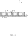
- FIG. 8 is a cross-sectional view showing a portion of the insulating adhesive of FIG. 7 removed to form an insulating adhesive layer.
- FIG. 9 is a cross-sectional view showing a second carrier plate formed on the insulating adhesive layer of FIG. 8 .
- FIG. 10 is a cross-sectional view showing a first outer component formed on a second outer wiring layer of the second carrier plate of FIG. 9 .
- FIG. 11 is a cross-sectional view showing a second outer component formed on a fourth outer wiring layer of the second carrier plate of FIG. 10 .
- FIG. 12 is a flowchart of a method for manufacturing a packaging structure according to the present disclosure.
- the present disclosure provides a method for manufacturing a circuit board.
- the method can be used to manufacture a double-sided circuit board and a multilayer circuit board.
- FIG. 12 the method for manufacturing a packaging structure is presented in accordance with an embodiment. The method is provided by way of example, as there are a variety of ways to carry out the method.
- the method can begin at S 1 .
- a first carrier plate 10 is provided.
- the first carrier plate 10 includes a first outer wiring layer 11 and a second outer wiring layer 12 stacked in a first direction X.
- the first outer wiring layer 11 and the second outer wiring layer 12 are electrically connected to each other.
- the first carrier plate 10 further includes at least one first intermediate wiring layer 13 located between the first outer wiring layer 11 and the second outer wiring layer 12 .
- Each first intermediate wiring layer 13 is electrically connected to the first outer wiring layer 11 and the second outer wiring layer 12 .
- the first carrier plate 10 can be manufactured from a metal cladding plate, which includes a second substrate layer 14 and two first metal foils (not shown) formed on two opposite surfaces of the second substrate layer 14 .
- the two first metal foils are then etched by a development and exposure process to obtain the first intermediate wiring layer 13 and the second outer wiring layer 12 .
- another second substrate layer 14 and another first metal foil are formed on the first intermediate wiring layer 13 .
- the first metal foil is then etched to form the first outer wiring layer 11 .
- a second insulating layer 140 is formed on the first outer wiring layer 11 .
- a second insulating layer 140 is also formed on the second insulating layer 140 .
- the second insulating layer 140 is sandwiched between the conductive layer 150 and the first outer wiring layer 11 .
- the second insulating layer 140 includes, but is not limited to, polypropylene (PP).
- At step S 3 referring to FIG. 3 , at least two second openings 160 are defined in the second insulating layer 140 .
- the second openings 160 may also be defined in the conductive layer 150 .
- Each second opening 160 extends along the first direction X, and a portion of the first outer wiring layer 11 is exposed from the second openings 160 .
- the second openings 160 are formed by laser cutting, which can improve an accuracy of size of the second openings 160 .
- the second openings 160 may be formed by mechanical drilling.
- a first conductive post 20 is formed in each second opening 160 . That is, at least two first conductive posts 20 are formed. The at least two first conductive posts 20 are arranged along a second direction Y perpendicular to the first direction X.
- a receiving groove 40 is defined in the second insulating layer 140 between adjacent first conductive posts 20 .
- Each first conductive post 20 includes a first end 21 , a second end 22 opposite to the first end 21 , and a sidewall 23 connected between the first end 21 and the second end 22 .
- the first end 21 is electrically connected to the first outer wiring layer 11 .
- the second end 22 is exposed from the first insulating layer 30 .
- a remaining portion of the second insulating layer 140 after forming the receiving grooves 40 , surrounds and covers the sidewalls 23 of all the first conductive post 20 to form a first insulating layer 30 .
- a width of each first conductive post 20 increases from the first end 21 to the second end 22 .
- step S 6 referring to FIG. 6 , an embedded component 50 is placed in each receiving groove 40 .
- a gap S is formed between each embedded component 50 and the corresponding receiving groove 40 .
- an insulating adhesive covers the first insulating layer 30 containing the first conductive posts 20 .
- the insulating adhesive is also forced into the gap S between each embedded component 50 and the receiving groove 40 by pressing.
- the insulating adhesive is cured, and a portion of the insulating adhesive is removed to expose the second end 22 . Thereby, a remaining portion of the insulating adhesive in the receiving groove 40 forms an insulating adhesive layer 60 .
- the insulating adhesive layer 60 is flush with the second end 22 .
- the insulating adhesive layer 60 fixes the embedded component 50 in the receiving groove 40 .
- the insulating adhesive may be removed by grinding.
- the insulating adhesive includes, but is not limited to, epoxy adhesive.
- steps S 7 and S 8 may be omitted. That is, the insulating adhesive may be directly filled in the receiving groove 40 and then cured to form the insulating adhesive layer 60 .
- a second carrier plate 90 is formed on the first insulating layer 30 including the first conductive posts 20 .
- the second carrier plate 90 further covers the insulating adhesive layer 60 and the embedded electronic component 50 in each receiving groove 40 .
- the second carrier plate 90 includes a third outer wiring layer 91 and a fourth outer wiring layer 92 stacked in the first direction X.
- the third outer wiring layer 91 is electrically connected to the second end 22 of each first conductive post 20 .
- the second carrier plate 90 can be manufactured after defining at least one first opening 70 in the insulating adhesive layer 60 .
- Each first opening 70 extends along the first direction X, and the pins of each embedded electronic component 50 are exposed from at least one first opening 70 .
- a metal layer (not shown) is then formed in each first opening 70 and on the insulating adhesive layer 60 and the first insulating layer 30 including the first conductive posts 20 by an electroplating process.
- the metal layer in each first opening 70 forms a second conductive post 80 , which is electrically connected to the corresponding embedded component 50 .
- the metal layer on the insulating adhesive layer 60 and the first insulating layer 30 including the first conductive posts 20 are then etched to form the third outer wiring layer 91 , and the third outer wiring layer 91 is connected to each embedded component 50 through the corresponding second conductive post 80 .
- a first substrate layer 93 and a second metal foil (not shown) are pressed on the third outer wiring layer 91 .
- the first substrate layer 93 is sandwiched between the second metal foil and the third outer wiring layer 91 .
- the second metal foil is etched to form the fourth outer wiring layer 92 .
- the second carrier plate 90 may further include at least one second intermediate wiring layer 94 between the third outer wiring layer 91 and the fourth outer wiring layer 92 .
- the at least one second intermediate wiring layer 94 is electrically connected to the third outer wiring layer 91 and the fourth outer wiring layer 92 .
- a line width of the first outer wiring layer 11 and the second outer wiring layer 12 is greater than that of the third outer wiring layer 91 and the fourth outer wiring layer 92 .
- a line width of the first intermediate wiring layer 13 is greater than that of the second intermediate wiring layer 94 .
- a first outer component 100 and a second outer component 110 are provided.
- the first outer component 100 is formed on and electrically connected to the second outer wiring layer 12 by a reflow soldering process.
- the second outer component 110 is formed on and electrically connected to the fourth outer wiring layer 92 also by the reflow soldering process. Thereby, the packaging structure 200 is obtained.
- the reflow soldering process can generate at least one first solder ball 120 that electrically connects the first outer component 100 to the second outer wiring layer 12 , and at least one second solder ball 130 that electrically connects the second outer component 110 to the fourth outer wiring layer 92 .
- the packaging structure 200 includes a first carrier plate 10 .
- the first carrier plate 10 includes a first outer wiring layer 11 and a second outer wiring layer 12 stacked in the first direction X.
- the first outer wiring layer 11 and the second outer wiring layer 12 are electrically connected to each other.
- At least two first conductive posts 20 are formed on the first outer wiring layer 11 , and the first conductive posts 20 are arranged along the second direction Y perpendicular to the first direction X.
- Each of the first conductive posts 20 includes a first end 21 , a second end 22 opposite to the first end 21 , and a sidewall 23 connected between the first end 21 and the second end 22 .
- the first end 21 is electrically connected to the first outer wiring layer 11 .
- a first insulating layer 30 surrounds the sidewalls 23 of all the first conductive posts 20 , and the second end 22 is exposed from the first insulating layer 30 .
- a receiving groove 40 is defined between adjacent first conductive posts 20 .
- An embedded component 50 is disposed in each receiving groove 40 . The embedded component 50 is connected and fixed to the first insulating layer 30 through an insulating adhesive layer 60 .
- the packaging structure 200 further includes a second carrier plate 90 .
- the second carrier plate 90 includes a third outer wiring layer 91 and a fourth outer wiring layer 92 stacked in the first direction X.
- the third outer wiring layer 91 is electrically connected to the second end 22 and the fourth outer wiring layer 92 .
- the second carrier plate 90 further includes at least one second conductive post 80 , which passes through the insulating adhesive layer 60 along the first direction X and electrically connects the third outer wiring layer 91 to the embedded component 50 .
- the packaging structure 200 further includes a first outer component 100 , a second outer component 110 , at least one first solder ball 120 , and at least one second solder ball 130 .
- the first solder ball 120 electrically connects the first outer component 100 to the second outer wiring layer 12 .
- the second solder ball 130 electrically connects the fourth outer wiring layer 92 to the second outer component 110 .
- the embedded component 50 may be a chip, and each of the first outer component 100 and the second outer component 110 may be a main board or a memory chip.
Landscapes
- Engineering & Computer Science (AREA)
- Microelectronics & Electronic Packaging (AREA)
- Manufacturing & Machinery (AREA)
- Production Of Multi-Layered Print Wiring Board (AREA)
- Combinations Of Printed Boards (AREA)
Abstract
Description
Claims (13)
Applications Claiming Priority (2)
| Application Number | Priority Date | Filing Date | Title |
|---|---|---|---|
| CN202210440061.4A CN116994964A (en) | 2022-04-25 | 2022-04-25 | Packaging structure and preparation method thereof |
| CN202210440061.4 | 2022-04-25 |
Publications (2)
| Publication Number | Publication Date |
|---|---|
| US20230345643A1 US20230345643A1 (en) | 2023-10-26 |
| US11864329B2 true US11864329B2 (en) | 2024-01-02 |
Family
ID=88415121
Family Applications (1)
| Application Number | Title | Priority Date | Filing Date |
|---|---|---|---|
| US17/824,020 Active 2042-08-05 US11864329B2 (en) | 2022-04-25 | 2022-05-25 | Packaging structure with embedded electronic components and method for manufacturing the same |
Country Status (3)
| Country | Link |
|---|---|
| US (1) | US11864329B2 (en) |
| CN (1) | CN116994964A (en) |
| TW (1) | TWI850661B (en) |
Families Citing this family (2)
| Publication number | Priority date | Publication date | Assignee | Title |
|---|---|---|---|---|
| CN115424997A (en) * | 2022-08-24 | 2022-12-02 | 矽力杰半导体技术(杭州)有限公司 | Integrated substrate and power integrated circuit |
| TWI896094B (en) * | 2024-04-23 | 2025-09-01 | 復盛精密工業股份有限公司 | Preformed conductive pillar structure combined with circuit and manufacturing method thereof |
Citations (5)
| Publication number | Priority date | Publication date | Assignee | Title |
|---|---|---|---|---|
| US20150062848A1 (en) * | 2013-08-29 | 2015-03-05 | Samsung Electro-Mechanics Co., Ltd. | Electronic component embedded substrate and method for manufacturing electronic component embedded substrate |
| US20160351543A1 (en) * | 2014-02-06 | 2016-12-01 | Lg Innotek Co., Ltd. | Printed circuit board, package substrate and production method for same |
| US20200015357A1 (en) * | 2018-07-09 | 2020-01-09 | Samsung Electro-Mechanics Co., Ltd. | Antenna substrate and antenna module including the same |
| US20200161248A1 (en) * | 2018-11-20 | 2020-05-21 | Samsung Electronics Co., Ltd. | Package module |
| US20200303314A1 (en) * | 2019-03-18 | 2020-09-24 | Samsung Electronics Co., Ltd. | Semiconductor package |
Family Cites Families (14)
| Publication number | Priority date | Publication date | Assignee | Title |
|---|---|---|---|---|
| US7989950B2 (en) * | 2008-08-14 | 2011-08-02 | Stats Chippac Ltd. | Integrated circuit packaging system having a cavity |
| US8658473B2 (en) * | 2012-03-27 | 2014-02-25 | General Electric Company | Ultrathin buried die module and method of manufacturing thereof |
| CN103681365B (en) * | 2012-08-31 | 2016-08-10 | 宏启胜精密电子(秦皇岛)有限公司 | Package-on-package structure and preparation method thereof |
| US9378982B2 (en) * | 2013-01-31 | 2016-06-28 | Taiwan Semiconductor Manufacturing Company, Ltd. | Die package with openings surrounding end-portions of through package vias (TPVs) and package on package (PoP) using the die package |
| JP2015176910A (en) * | 2014-03-13 | 2015-10-05 | 株式会社東芝 | semiconductor memory |
| US10276548B2 (en) * | 2016-09-14 | 2019-04-30 | Taiwan Semiconductor Manufacturing Company, Ltd. | Semiconductor packages having dummy connectors and methods of forming same |
| CN106876364A (en) * | 2017-03-15 | 2017-06-20 | 三星半导体(中国)研究开发有限公司 | Semiconductor package assembly and a manufacturing method thereof |
| US10727198B2 (en) * | 2017-06-30 | 2020-07-28 | Taiwan Semiconductor Manufacturing Co., Ltd. | Semiconductor package and method manufacturing the same |
| US10636775B2 (en) * | 2017-10-27 | 2020-04-28 | Taiwan Semiconductor Manufacturing Co., Ltd. | Package structure and manufacturing method thereof |
| EP3483921B1 (en) * | 2017-11-11 | 2026-01-07 | AT & S Austria Technologie & Systemtechnik Aktiengesellschaft | Embedding known-good component in known-good cavity of known-good component carrier material with pre-formed electric connection structure |
| US10515848B1 (en) * | 2018-08-01 | 2019-12-24 | Taiwan Semiconductor Manufacturing Company, Ltd. | Semiconductor package and method |
| US10665520B2 (en) * | 2018-10-29 | 2020-05-26 | Taiwan Semiconductor Manufacturing Company, Ltd. | Integrated circuit package and method |
| TWI707408B (en) * | 2019-04-10 | 2020-10-11 | 力成科技股份有限公司 | Integrated antenna package structure and manufacturing method thereof |
| US11652037B2 (en) * | 2020-07-31 | 2023-05-16 | Taiwan Semiconductor Manufacturing Co., Ltd. | Semiconductor package and method of manufacture |
-
2022
- 2022-04-25 CN CN202210440061.4A patent/CN116994964A/en active Pending
- 2022-05-11 TW TW111117688A patent/TWI850661B/en active
- 2022-05-25 US US17/824,020 patent/US11864329B2/en active Active
Patent Citations (5)
| Publication number | Priority date | Publication date | Assignee | Title |
|---|---|---|---|---|
| US20150062848A1 (en) * | 2013-08-29 | 2015-03-05 | Samsung Electro-Mechanics Co., Ltd. | Electronic component embedded substrate and method for manufacturing electronic component embedded substrate |
| US20160351543A1 (en) * | 2014-02-06 | 2016-12-01 | Lg Innotek Co., Ltd. | Printed circuit board, package substrate and production method for same |
| US20200015357A1 (en) * | 2018-07-09 | 2020-01-09 | Samsung Electro-Mechanics Co., Ltd. | Antenna substrate and antenna module including the same |
| US20200161248A1 (en) * | 2018-11-20 | 2020-05-21 | Samsung Electronics Co., Ltd. | Package module |
| US20200303314A1 (en) * | 2019-03-18 | 2020-09-24 | Samsung Electronics Co., Ltd. | Semiconductor package |
Also Published As
| Publication number | Publication date |
|---|---|
| CN116994964A (en) | 2023-11-03 |
| US20230345643A1 (en) | 2023-10-26 |
| TW202343696A (en) | 2023-11-01 |
| TWI850661B (en) | 2024-08-01 |
Similar Documents
| Publication | Publication Date | Title |
|---|---|---|
| US6969916B2 (en) | Substrate having built-in semiconductor apparatus and manufacturing method thereof | |
| US5831833A (en) | Bear chip mounting printed circuit board and a method of manufacturing thereof by photoetching | |
| US20100242272A1 (en) | Method of manufacturing printed circuit board | |
| JPWO2008155957A1 (en) | Manufacturing method of component-embedded substrate and component-embedded substrate | |
| CN101026103A (en) | Package on package with cavity and method for manufacturing thereof | |
| US20130122216A1 (en) | Structure of embedded-trace substrate and method of manufacturing the same | |
| US11864329B2 (en) | Packaging structure with embedded electronic components and method for manufacturing the same | |
| CN109788665B (en) | Circuit substrate containing electronic components and method of making the same | |
| US10062623B2 (en) | Semiconductor package substrate, package system using the same and method for manufacturing thereof | |
| CN119725107B (en) | Chip packaging structure and method | |
| US20090008766A1 (en) | High-Density Fine Line Structure And Method Of Manufacturing The Same | |
| US12191240B2 (en) | Hybrid glass core for wafer level and panel level packaging applications | |
| JP2022036015A (en) | Embedded structure and manufacturing method thereof and substrate | |
| CN107046016A (en) | Reduced size through hole land structure and method of manufacturing the same | |
| US7963031B2 (en) | Package for semiconductor device and method of manufacturing the same | |
| KR101502428B1 (en) | Semiconductor package and method for manufacturing the same | |
| KR101278426B1 (en) | Manufacturing method of Semiconductor package substrate | |
| US7445961B2 (en) | Semiconductor chip package and method for fabricating the same | |
| US20160315027A1 (en) | Semiconductor package and method of manufacturing the same | |
| KR102052761B1 (en) | Chip Embedded Board And Method Of Manufacturing The Same | |
| JP2003031954A (en) | Multilayer substrate with built-in electronic components and method of manufacturing the same | |
| KR101969643B1 (en) | Rigid flexible circuit board manufacturing method | |
| CN111356302B (en) | Circuit board and manufacturing method thereof | |
| US20240243021A1 (en) | Package carrier and manufacturing method thereof and chip package structure | |
| US20240170301A1 (en) | Packaging structure, packaging substrate, and manufacturing method of the packaging structure |
Legal Events
| Date | Code | Title | Description |
|---|---|---|---|
| AS | Assignment |
Owner name: AVARY HOLDING (SHENZHEN) CO., LIMITED., CHINA Free format text: ASSIGNMENT OF ASSIGNORS INTEREST;ASSIGNORS:FU, CHIH-CHIEH;LIN, YUAN-YU;LI, ZE-JIE;REEL/FRAME:060010/0603 Effective date: 20220523 Owner name: HONGQISHENG PRECISION ELECTRONICS (QINHUANGDAO) CO.,LTD., CHINA Free format text: ASSIGNMENT OF ASSIGNORS INTEREST;ASSIGNORS:FU, CHIH-CHIEH;LIN, YUAN-YU;LI, ZE-JIE;REEL/FRAME:060010/0603 Effective date: 20220523 |
|
| FEPP | Fee payment procedure |
Free format text: ENTITY STATUS SET TO UNDISCOUNTED (ORIGINAL EVENT CODE: BIG.); ENTITY STATUS OF PATENT OWNER: LARGE ENTITY |
|
| STPP | Information on status: patent application and granting procedure in general |
Free format text: NOTICE OF ALLOWANCE MAILED -- APPLICATION RECEIVED IN OFFICE OF PUBLICATIONS |
|
| STPP | Information on status: patent application and granting procedure in general |
Free format text: PUBLICATIONS -- ISSUE FEE PAYMENT RECEIVED |
|
| STPP | Information on status: patent application and granting procedure in general |
Free format text: PUBLICATIONS -- ISSUE FEE PAYMENT VERIFIED |
|
| STCF | Information on status: patent grant |
Free format text: PATENTED CASE |