US11862901B2 - Interposer - Google Patents
Interposer Download PDFInfo
- Publication number
- US11862901B2 US11862901B2 US17/122,579 US202017122579A US11862901B2 US 11862901 B2 US11862901 B2 US 11862901B2 US 202017122579 A US202017122579 A US 202017122579A US 11862901 B2 US11862901 B2 US 11862901B2
- Authority
- US
- United States
- Prior art keywords
- interposer
- current
- pcb
- coaxial cables
- pcbs
- Prior art date
- Legal status (The legal status is an assumption and is not a legal conclusion. Google has not performed a legal analysis and makes no representation as to the accuracy of the status listed.)
- Active, expires
Links
Images


Classifications
-
- G—PHYSICS
- G01—MEASURING; TESTING
- G01R—MEASURING ELECTRIC VARIABLES; MEASURING MAGNETIC VARIABLES
- G01R1/00—Details of instruments or arrangements of the types included in groups G01R5/00 - G01R13/00 and G01R31/00
- G01R1/02—General constructional details
- G01R1/04—Housings; Supporting members; Arrangements of terminals
- G01R1/0408—Test fixtures or contact fields; Connectors or connecting adaptors; Test clips; Test sockets
- G01R1/0416—Connectors, terminals
-
- H—ELECTRICITY
- H01—ELECTRIC ELEMENTS
- H01R—ELECTRICALLY-CONDUCTIVE CONNECTIONS; STRUCTURAL ASSOCIATIONS OF A PLURALITY OF MUTUALLY-INSULATED ELECTRICAL CONNECTING ELEMENTS; COUPLING DEVICES; CURRENT COLLECTORS
- H01R13/00—Details of coupling devices of the kinds covered by groups H01R12/70 or H01R24/00 - H01R33/00
- H01R13/648—Protective earth or shield arrangements on coupling devices, e.g. anti-static shielding
- H01R13/658—High frequency shielding arrangements, e.g. against EMI [Electro-Magnetic Interference] or EMP [Electro-Magnetic Pulse]
- H01R13/6581—Shield structure
- H01R13/6585—Shielding material individually surrounding or interposed between mutually spaced contacts
- H01R13/6586—Shielding material individually surrounding or interposed between mutually spaced contacts for separating multiple connector modules
- H01R13/6587—Shielding material individually surrounding or interposed between mutually spaced contacts for separating multiple connector modules for mounting on PCBs
-
- H—ELECTRICITY
- H01—ELECTRIC ELEMENTS
- H01R—ELECTRICALLY-CONDUCTIVE CONNECTIONS; STRUCTURAL ASSOCIATIONS OF A PLURALITY OF MUTUALLY-INSULATED ELECTRICAL CONNECTING ELEMENTS; COUPLING DEVICES; CURRENT COLLECTORS
- H01R12/00—Structural associations of a plurality of mutually-insulated electrical connecting elements, specially adapted for printed circuits, e.g. printed circuit boards [PCB], flat or ribbon cables, or like generally planar structures, e.g. terminal strips, terminal blocks; Coupling devices specially adapted for printed circuits, flat or ribbon cables, or like generally planar structures; Terminals specially adapted for contact with, or insertion into, printed circuits, flat or ribbon cables, or like generally planar structures
- H01R12/50—Fixed connections
- H01R12/51—Fixed connections for rigid printed circuits or like structures
- H01R12/515—Terminal blocks providing connections to wires or cables
-
- H—ELECTRICITY
- H01—ELECTRIC ELEMENTS
- H01R—ELECTRICALLY-CONDUCTIVE CONNECTIONS; STRUCTURAL ASSOCIATIONS OF A PLURALITY OF MUTUALLY-INSULATED ELECTRICAL CONNECTING ELEMENTS; COUPLING DEVICES; CURRENT COLLECTORS
- H01R13/00—Details of coupling devices of the kinds covered by groups H01R12/70 or H01R24/00 - H01R33/00
- H01R13/02—Contact members
- H01R13/22—Contacts for co-operating by abutting
- H01R13/24—Contacts for co-operating by abutting resilient; resiliently-mounted
- H01R13/2407—Contacts for co-operating by abutting resilient; resiliently-mounted characterized by the resilient means
- H01R13/2428—Contacts for co-operating by abutting resilient; resiliently-mounted characterized by the resilient means using meander springs
-
- H—ELECTRICITY
- H01—ELECTRIC ELEMENTS
- H01R—ELECTRICALLY-CONDUCTIVE CONNECTIONS; STRUCTURAL ASSOCIATIONS OF A PLURALITY OF MUTUALLY-INSULATED ELECTRICAL CONNECTING ELEMENTS; COUPLING DEVICES; CURRENT COLLECTORS
- H01R13/00—Details of coupling devices of the kinds covered by groups H01R12/70 or H01R24/00 - H01R33/00
- H01R13/46—Bases; Cases
- H01R13/514—Bases; Cases composed as a modular blocks or assembly, i.e. composed of co-operating parts provided with contact members or holding contact members between them
-
- H—ELECTRICITY
- H01—ELECTRIC ELEMENTS
- H01R—ELECTRICALLY-CONDUCTIVE CONNECTIONS; STRUCTURAL ASSOCIATIONS OF A PLURALITY OF MUTUALLY-INSULATED ELECTRICAL CONNECTING ELEMENTS; COUPLING DEVICES; CURRENT COLLECTORS
- H01R2201/00—Connectors or connections adapted for particular applications
- H01R2201/20—Connectors or connections adapted for particular applications for testing or measuring purposes
-
- H—ELECTRICITY
- H01—ELECTRIC ELEMENTS
- H01R—ELECTRICALLY-CONDUCTIVE CONNECTIONS; STRUCTURAL ASSOCIATIONS OF A PLURALITY OF MUTUALLY-INSULATED ELECTRICAL CONNECTING ELEMENTS; COUPLING DEVICES; CURRENT COLLECTORS
- H01R9/00—Structural associations of a plurality of mutually-insulated electrical connecting elements, e.g. terminal strips or terminal blocks; Terminals or binding posts mounted upon a base or in a case; Bases therefor
- H01R9/03—Connectors arranged to contact a plurality of the conductors of a multiconductor cable, e.g. tapping connections
- H01R9/05—Connectors arranged to contact a plurality of the conductors of a multiconductor cable, e.g. tapping connections for coaxial cables
- H01R9/0506—Connection between three or more cable ends
Definitions
- This specification describes examples of interposers configured to act as interfaces to a device, such as a device interface board (DIB) in a test system.
- DIB device interface board
- An example interposer includes an interconnect for transmitting signals between a source and a destination.
- an interposer may include electrical pathways to transmit electrical signals between components of a system.
- An interposer for a test system includes coaxial cables, each of which is configured to transport a first portion of current originating from a current source, and printed circuit boards (PCBs), each of which is connected to a set of the coaxial cables in order to receive the first portion of the current from each coaxial cable in the set and to transport a second portion of the current.
- a spring leaf assembly includes spring leaves, each of which is connected to a PCB in order to transport a third portion of the current obtained from the PCB to a device interface board (DIB) that connects to devices under test (DUTs) to be tested by the test system.
- DIB device interface board
- the coaxial cables on each PCB including the inner and outer conductors of the coaxial cables on each PCB, are arranged in parallel, the PCBs are arranged in parallel, and the spring leaves on each PCB are arranged in parallel.
- the example interposer may include one or more of the following features, either alone or in combination.
- the interposer may have an inductance of 100 nanohenries (nH) or less for a current of 2000 amperes (A) or more.
- the interposer may have a resistance of 3 milliohms (m ⁇ ) or less for a current of 2000 amperes (A) or more.
- the interposer may have an inductance of 500 nanohenries (nH) or less for a current of 2000 amperes (A) or more.
- the interposer may have a resistance of 10 milliohms (m ⁇ ) or less for a current of 2000 amperes (A) or more.
- the first portion of the current may be different from the second portion of the current.
- the first portion of the current may be equal to the third portion of the current.
- the second portion of the current may be different from the third portion of the current.
- the second portion of the current may be different from the third portion and the first portion.
- Each coaxial cable may include a center conductor and shield surrounding the center conductor.
- the shield may include a return for current transmitted through the center conductor.
- the shield and the center conductor may implement a least some inductance cancellation.
- the shield and the center conductor may maximize inductance cancellation.
- the interposer may include a shroud comprised of electrically-insulating insulating material.
- the shroud may be at least partly around the spring leaf assembly.
- the interposer may be part of a blind-mate connection within a test head of the test system.
- the interposer may include electrically-insulating material separating each of the PCBs.
- Each PCB may include a surge suppressor to protect against voltage spikes or current spikes on the PCB.
- the coaxial cables, the PCBs, and the spring leaves may be configured and arranged to achieve a target resistance and a target inductance of the interposer.
- the interposer may connect to low-inductance copper pads on the DIB within an area that is 2 inches (5.08 centimeters (cm)) by 3 inches (7.62 cm) or less.
- An example test system includes a device interface board (DIB) to connect to devices under test (DUTs) and a test head comprising a blind-mate connection to the DIB.
- the blind-mate connection includes an interposer assembly.
- the interposer assembly includes coaxial cables, each of which is configured to transport a first portion of current originating from a current source, and printed circuit boards (PCBs), each of which is connected to a set of the coaxial cables in order to receive the first portion of the current from each coaxial cable in the set and to transport a second portion of the current.
- a spring leaf assembly includes spring leaves, each of which is connected to a PCB in order to transport a third portion of the current obtained from the PCB to the DIB.
- the coaxial cables on each PCB are arranged in parallel, the PCBs are arranged in parallel, and the spring leaves on each PCB are arranged in parallel.
- the example test system may include one or more of the following features, either alone or in combination.
- the coaxial cables may have lengths defined in double-digit meters or less, lengths defined in single-digit meters or less, lengths defined in single-digit decimeters or less, or lengths defined in single-digit centimeters or less.
- the coaxial cables, the PCBs, and the spring leaves may be configured and arranged to reduce, or to minimize, the resistance and the inductance of the interposer assembly.
- the coaxial cables, the PCBs, and the spring leaves may be configured and arranged to implement a target resistance and a target inductance of the interposer assembly.
- At least part of the systems and techniques described in this specification may be configured or controlled by executing, on one or more processing devices, instructions that are stored on one or more non-transitory machine-readable storage media.
- non-transitory machine-readable storage media include read-only memory, an optical disk drive, memory disk drive, and random access memory.
- At least part of the systems and techniques described in this specification may be configured or controlled using a computing system comprised of one or more processing devices and memory storing instructions that are executable by the one or more processing devices to perform various control operations including high-current testing.
- At least some of the devices, systems, and/or components described herein may be configured, for example through design, construction, arrangement, placement, programming, operation, activation, deactivation, and/or control.
- FIG. 1 is a side view drawing of an example interposer.
- FIG. 2 is a side perspective view drawing of the example interposer.
- FIG. 3 is a front perspective view drawing of the example interposer.
- FIG. 4 is a top perspective photograph of the example interposer.
- FIG. 5 is block diagram of an example test system that includes the interposer.
- FIG. 6 shows example pads to which the interposer connects.
- An example interposer includes an interconnect for transmitting signals between a source and a destination.
- the interposer may include electrical conductors to transmit electrical signals between components of a test system.
- An example interposer includes coaxial cables, each of which is configured to transport a first portion of current originating from a current source.
- the example interposer also includes printed circuit boards (PCBs), each of which is connected to a set of the coaxial cables in order to receive the first portion of the current from each coaxial cable in the set and to transport a second portion of the current.
- a spring leaf assembly includes spring leaves, each which is connected to a PCB in order to transport a third portion of the current obtained from the PCB to a device interface board (DIB) that connects to devices under test (DUTs) to be tested by the test system.
- DIB device interface board
- Inner and outer conductors of the coaxial cables on each PCB are arranged in parallel, the PCBs are arranged in parallel, and the spring leaves on each PCB may be arranged in parallel.
- Implementations of the interposer may enable relatively high currents to be transmitted through the interposer at relatively low inductances and resistances.
- inductance includes the tendency of an electrical conductor to oppose a change in current flowing therethrough. Resistance is a measure of the opposition to current flow through a conductor. It is therefore preferable to keep inductance and resistance values low.
- the current through the interposer is pulsed at least part of the time or all of the time.
- a pulsed current may include a rapid, transient change in amplitude from a baseline value such as “0” to a higher or lower value, followed by a rapid return to the baseline value.
- the current is periodic, for example. Reducing inductance reduces the opposition to changes in current such as these.
- Examples of high current include, but are not limited to, currents over 500 Amperes (A), over 1000 A, over 2000 A, over 3000 A, or more.
- Examples of low inductance include, but are not limited to 100 nanoHenries (nH) to 60 nH or less. Examples of low resistance include 10 milliohms ( ⁇ ) or less or 3 m ⁇ or less.
- Implementations of the interposer may be relatively small in terms of physical dimensions.
- the interposer may connect to low-inductance copper pads 80 on the DIB (or on a probe card, for example) on an area of the DIB (or probe card) within an area that is 2 inches (5.08 centimeters (cm)) by 3 inches (7.62 cm) or less.
- the interposer connects to the DIB within an area that is 1.5 inches (3.81 cm) by 2.5 inches (6.35 cm).
- the parallel conductors included in the interposer may enable such small sizes while maintaining relatively low resistance and inductance values even at relatively high currents.
- interposers having the features described herein are not limited to any particular dimensions or values of resistance, inductance, or current.
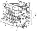
- FIGS. 1 to 4 shows an example implementation of an interposer 10 that may have features like those described in the preceding paragraphs.
- Interposer 10 includes PCBs 12 , 13 , 14 , 15 , 16 , and 17 . Although six PCBs are included in the implementation of FIGS. 1 to 4 , interposer 10 may include more than six PCBs or fewer than six PCBs.
- Each PCB includes a non-conductive substrate such as G10 FR-4, which is a glass-reinforced epoxy laminate material.
- One or more electrically-conductive conduits run through or over the substrate to carry electrical signals, such as current, from the input of each PCB to the output of each PCB. Generally, the more signal pathways that there are through a PCB, the lower will be the resistance and inductance of that PCB.
- Non-conductive spacers 20 , 21 , 22 , 23 , and 24 separate adjacent PCBs within the interposer.
- Non-conductive spacers 20 to 24 may be made of G10 FR-4 or any appropriate dielectric—that is, an electrically-non-conductive material.
- each PCB may also include a surge suppressor 26 to protect against voltage spikes or current spikes on that PCB.
- the input to each PCB includes multiple coaxial cables 30 .
- Each of the coaxial cables 30 may connect to the PCB using edge plating 29 , in which each cable is spliced and soldered to the PCB.
- interposer 10 may include more than six coaxial cables per PCB or fewer than six coaxial cables per PCB. Accordingly, in the example of FIGS. 1 to 4 , there are 36 coaxial cables in total on interposer 10 .
- a coaxial cable includes an inner conductor surrounded by a concentric conducting shield.
- Each coaxial cable also includes a protective outer sheath that is also non-conductive.
- Current passes through the inner conductor of each coaxial cable 30 , with the concentric conducting shield acting as a return path for current.
- force-high (or positive) current may pass through the inner conductor and force-low (or negative) current may pass through the outer conductor, where force-high currents and force-low currents correspond to currents having different polarities.
- Use of the center conductor and the concentric conductive shield to transmit force-current high and force-current low signals, respectively, may limit or reduce inductance in the coaxial cables through inductance cancellation effects.
- thin dielectrics such as in a range of 2 mils (0.5 millimeters (mm)) to 10 mils (0.25 mm), may also contribute to inductance cancellation.
- the coaxial cables for a PCB connect electrically to the electrically-conductive conduits in the PCB via an edge plating technique.
- the inner conductor of a coaxial cable may connect electrically to a first set of the electrically-conductive conduits in the PCB, where the first set may include one or more of the electrically-conductive conduits.
- the outer (or return) conductor of the same coaxial cable may connect electrically to a second set of the electrically-conductive conduits in the PCB, where the second set may include one or more of the electrically-conductive conduits that are different than the first set.
- Different coaxial cables may connect in this way to different sets of conduits on a PCB.
- PCB 17 Current from the coaxial cables connected to a PCB, such as PCB 17 , thus runs through that PCB, with a return path also running through the PCB.
- sets of electrically-conductive conduits on the PCB that transport current having different polarities are adjacent. For example, no two sets of electrically-conductive conduits on a PCB may transport current of the same polarity. This may produce at least some inductive cancellation on the PCB.
- each PCB 12 to 17 also includes a spring leaf assembly 40 (see FIG. 1 ).
- Each PCB may include edge plating to implement such connections.
- Each spring leaf assembly 40 includes multiple leaves 41 , 42 , 43 , and 44 .
- Each leaf includes an electrically-conductive material that is connectable, electrically, to one or more of the electrically-conductive conduits on the PCB.
- a leaf may include a pre-loaded spring finger that is compressible to provide a stable electrical contact. As shown in FIGS. 1 and 3 , in some implementations there are four spring leaves on each PCB; however, in some implementations there may be different numbers of spring leaves per PCB.
- each of the spring leaves is connected to a corresponding PCB in order to transport a portion of the current obtained from the PCB to a device interface board (DIB) of a test system.
- the spring leaf connectors may be arranged to alternate in polarity. For example, in a case where there are four spring leaf connectors on a PCB, a first leaf connector 41 may be for a force-high current path, a second leaf connector 42 adjacent to the first leaf connector may be for a force-low or return current path, a third leaf connector 43 adjacent to the second leaf connector may be for a force-high current path, and a fourth leaf connector 44 adjacent to the third leaf connector may be for a force-low or return current path.
- the first (force-high) leaf connector 41 may connect electrically to a first set of the electrically-conductive conduits in the PCB, where the first set may include one or more of the electrically-conductive conduits.
- the second (force-low or return) leaf connector 42 may connect electrically to a second set of the electrically-conductive conduits in the PCB, where the second set may include one or more of the electrically-conductive conduits that are different than the first set.
- the third (force-high) leaf connector 43 may connect electrically to a third set of the electrically-conductive conduits in the PCB, where the third set may include one or more of the electrically-conductive conduits that are different than the first set and the second set.
- the fourth (force-low or return) leaf connector 44 may connect electrically to a fourth set of the electrically-conductive conduits in the PCB, where the fourth set may include one or more of the electrically-conductive conduits that are different than the first set, the second set, and the third set.
- the coaxial cables 30 on each PCB are arranged in parallel with each other, the PCBs are arranged in parallel with each other, and the spring leaves 40 on each PCB are arranged in parallel with each other.
- the groups of coaxial cables (in this example, six coaxial cables) on each PCB are also in parallel with each other.
- the groups of spring leaf connectors (in this example, four spring leaf connectors) on each PCB are also in parallel with each other. Use of parallel connections such as these, provide support for high levels of current, such as, but not limited to, currents over 500 Amperes (A), 1000 A or more, 2000 A or more, or 3000 A or more.
- parallel connections such as these, also provide support for low levels of current, such as currents of less than 500 A, less than 5 A, less than 1 A, and into or below the single-digit milliampere range.
- inductance in the interposer can be limited or reduced to, for example, 100 nanoHenries (nH) to 60 nH or less.
- the multiple parallel paths also function to limit or to reduce resistance in the interposer.
- pulsed current of 2000 Amps on the force and return each passing through the interposer 10 .
- each of the coaxial cables transports a different portion of pulsed current than each of the PCBs and each of the spring leaf connectors; each of the spring leaf connectors transports a different portion of current than each of the PCBs and each of the coaxial cables; and each of the PCBs transports a different portion of current than each of the PCBs and each of the spring leaf connectors.
- the number of spring leaf connectors may be increased so that the portions of current transmitted by each spring leaf connector and each coaxial cable are equal.
- different PCBs may include different numbers of coaxial cable connections and different numbers of spring leaf connections.
- the coaxial cables, the PCBs, and the spring leaves may be configured and arranged to minimize the resistance and the inductance of the interposer assembly.
- a computer program may be executed to simulate various configurations of the interposer and the configuration that produces the lowest resistance and inductance for a given current or range of currents may be selected.
- the coaxial cables, the PCBs, and the spring leaves may be configured and arranged to reduce the resistance and the inductance of the interposer assembly. For example, increasing the numbers of conductive paths, while maintaining them in parallel may reduce these characteristics of the interposer.
- the spring leaves may be configured and arranged to implement a target resistance and a target inductance of the interposer assembly. For example, by selecting the numbers and arrangements of components of the interposer—e.g., the PCBs, the coaxial connections, and the spring leaves—it is possible to produce specific resistance and inductance in the interposer.
- interposer 10 includes a shroud 50 comprised of electrically-insulating insulating material.
- Shroud 50 is at least partly around spring leaf assembly, particularly the areas where human contact with electrical conductors is possible.
- shroud 50 surrounds the entire spring leaf assembly.
- shroud 50 is around sides of the spring leaf assembly and extends partway along sides of the PCBs to cover any electrical connections that may exist along the sides of the PCBs.
- interposer 10 may be used to make a blind mate connection to gold or copper pads a DIB or a probe card holding DUTs to be tested by a test system such as automatic test equipment (ATE).
- ATE automatic test equipment
- the blind-mate connection may be within a test head of the ATE.
- a blind-mate connector includes self-aligning features that guide the connector into the correct mating position. Connections to the gold or copper pads may alternate in polarity such that each positive connection is next to each negative connection, thereby reducing inductance
- an example test system such as ATE 70 may include a current source 71 , a polarity inverter 72 , an interposer 73 of the type described herein, and a DIB 74 .
- the interposer may have an inductance of 100 nh or less for a pulsed current of 2000 A or more.
- the interposer may have a resistance of 3 milliohms (m ⁇ ) or less for a current of 2000 A or more.
- the interposer may have an inductance of 500 nH or less for a pulsed current of 2000 A or more.
- the interposer may have a resistance of 10 m ⁇ or less for a pulsed current of 2000 A or more.
- polarity inverter 72 During operation, current flows from the current source through the polarity inverter 72 , where its polarity is either kept the same or changed based on requirements to test DUTs connected to the test system. In some examples, the polarity inverter may be omitted.
- Current output from the polarity inverter is passed to interposer 73 which, in this example includes an electrical and/or mechanical interface to DIB 74 .
- the current is passed from polarity inverter 72 to interposer 73 over coaxial cables, such as coaxial cables 30 . Current from the interposer then passes to the DIB.
- the DIB holds DUTs in sites 75 for testing and distributes the current from interposer 73 to the DUTs in the sites for testing.
- multiple interposers of the type described herein may be connected to a single DIB.
- the coaxial cables each have a length of 13 meters or 13.5 meters; however, different lengths may be used.
- the coaxial cables each may have lengths defined in triple-digit meters or less; the coaxial cables each may have lengths defined in double-digit meters or less; the coaxial cables each may have lengths defined in single-digit meters or less; the coaxial cables each may have lengths defined in single-digit decimeters or less; or the coaxial cables each may have lengths defined in single-digit centimeters or less.
- electrical conduits other than coaxial cables may be used.
- ATE 70 also includes a control system 76 .
- the control system may include a computing system comprised of one or more microprocessors or other appropriate processing devices as described herein. Communication between the control system and the other components of ATE 70 is represented conceptually by line 77 .
- DIB 74 includes a PCB having sites that include mechanical and electrical interfaces to one or more DUTs that are being tested or are to be tested by the ATE. Power, including voltage, may be run via one or more layers in the DIB to DUTs connected to the DIB. DIB 74 also may include one or more ground layers and one or signal layers with connected vias for transmitting signals to the DUTs.
- Sites 75 may include pads, conductive traces, or other points of electrical and mechanical connection to which the DUTs may connect. Test signals and response signals, including high current signals pass via test channels over the sites between the DUTs and test instruments. DIB 74 may also include, among other things, connectors, conductive traces, conductive layers, and circuitry for routing signals between test instruments, DUTs connected to sites 75 , and other circuitry.
- Control system 76 communicates with test instruments (not shown) to control testing. Control system 76 may also configure the polarity inverter 72 to provide voltage/current at the polarity required for testing. The control may be adaptive in that the polarity may be changed during testing if desired or required.
- test systems described in this specification and their various modifications may be configured or controlled at least in part by one or more computers such as control system 76 using one or more computer programs tangibly embodied in one or more information carriers, such as in one or more non-transitory machine-readable storage media.
- a computer program can be written in any form of programming language, including compiled or interpreted languages, and it can be deployed in any form, including as a stand-alone program or as a module, part, subroutine, or other unit suitable for use in a computing environment.
- a computer program can be deployed to be executed on one computer or on multiple computers at one site or distributed across multiple sites and interconnected by a network.
- Actions associated with configuring or controlling the test system described herein can be performed by one or more programmable processors executing one or more computer programs to control or to perform all or some of the operations described herein. All or part of the test systems and processes can be configured or controlled by special purpose logic circuitry, such as, an FPGA (field programmable gate array) and/or an ASIC (application-specific integrated circuit) or embedded microprocessor(s) localized to the instrument hardware.
- special purpose logic circuitry such as, an FPGA (field programmable gate array) and/or an ASIC (application-specific integrated circuit) or embedded microprocessor(s) localized to the instrument hardware.
- processors suitable for the execution of a computer program include, by way of example, both general and special purpose microprocessors, and any one or more processors of any kind of digital computer.
- a processor will receive instructions and data from a read-only storage area or a random access storage area or both.
- Elements of a computer include one or more processors for executing instructions and one or more storage area devices for storing instructions and data.
- a computer will also include, or be operatively coupled to receive data from, or transfer data to, or both, one or more machine-readable storage media, such as mass storage devices for storing data, such as magnetic, magneto-optical disks, or optical disks.
- Non-transitory machine-readable storage media suitable for embodying computer program instructions and data include all forms of non-volatile storage area, including by way of example, semiconductor storage area devices, such as EPROM (erasable programmable read-only memory), EEPROM (electrically erasable programmable read-only memory), and flash storage area devices; magnetic disks, such as internal hard disks or removable disks; magneto-optical disks; and CD-ROM (compact disc read-only memory) and DVD-ROM (digital versatile disc read-only memory).
- semiconductor storage area devices such as EPROM (erasable programmable read-only memory), EEPROM (electrically erasable programmable read-only memory), and flash storage area devices
- magnetic disks such as internal hard disks or removable disks
- magneto-optical disks magneto-optical disks
- CD-ROM compact disc read-only memory
- DVD-ROM digital versatile disc read-only memory
Landscapes
- Physics & Mathematics (AREA)
- General Physics & Mathematics (AREA)
- Measuring Leads Or Probes (AREA)
- Tests Of Electronic Circuits (AREA)
Abstract
Description
Claims (25)
Priority Applications (5)
| Application Number | Priority Date | Filing Date | Title |
|---|---|---|---|
| US17/122,579 US11862901B2 (en) | 2020-12-15 | 2020-12-15 | Interposer |
| PCT/US2021/062039 WO2022132483A1 (en) | 2020-12-15 | 2021-12-06 | Interposer |
| CN202180083526.9A CN116569052A (en) | 2020-12-15 | 2021-12-06 | insert |
| KR1020237021150A KR20230118589A (en) | 2020-12-15 | 2021-12-06 | interposer |
| JP2023535630A JP2023553163A (en) | 2020-12-15 | 2021-12-06 | interposer |
Applications Claiming Priority (1)
| Application Number | Priority Date | Filing Date | Title |
|---|---|---|---|
| US17/122,579 US11862901B2 (en) | 2020-12-15 | 2020-12-15 | Interposer |
Publications (2)
| Publication Number | Publication Date |
|---|---|
| US20220190527A1 US20220190527A1 (en) | 2022-06-16 |
| US11862901B2 true US11862901B2 (en) | 2024-01-02 |
Family
ID=81941915
Family Applications (1)
| Application Number | Title | Priority Date | Filing Date |
|---|---|---|---|
| US17/122,579 Active 2041-09-01 US11862901B2 (en) | 2020-12-15 | 2020-12-15 | Interposer |
Country Status (5)
| Country | Link |
|---|---|
| US (1) | US11862901B2 (en) |
| JP (1) | JP2023553163A (en) |
| KR (1) | KR20230118589A (en) |
| CN (1) | CN116569052A (en) |
| WO (1) | WO2022132483A1 (en) |
Families Citing this family (2)
| Publication number | Priority date | Publication date | Assignee | Title |
|---|---|---|---|---|
| CN120569857A (en) * | 2022-11-25 | 2025-08-29 | 豪倍公司 | Multi-port connector |
| GB2634713A (en) * | 2023-10-09 | 2025-04-23 | The Magstim Company Ltd | Magnetic stimulation coil system |
Citations (148)
| Publication number | Priority date | Publication date | Assignee | Title |
|---|---|---|---|---|
| US3516077A (en) | 1968-05-28 | 1970-06-02 | Bell Telephone Labor Inc | Magnetic propagation device wherein pole patterns move along the periphery of magnetic disks |
| US3577131A (en) | 1969-01-30 | 1971-05-04 | Bell Telephone Labor Inc | Domain propagation arrangement |
| US3673433A (en) | 1970-08-21 | 1972-06-27 | Siemens Ag Albis | Circuit arrangement for selectively connecting at least two inputs to a counting stage possessing at least one preparatory input and one triggering input and including contact bounce suppression circuitry |
| US3934236A (en) | 1974-01-11 | 1976-01-20 | Monsanto Company | Pulsed field accessed bubble propagation circuits |
| US4021790A (en) | 1974-01-11 | 1977-05-03 | Monsanto Company | Mutually exclusive magnetic bubble propagation circuits |
| US4117543A (en) | 1972-08-24 | 1978-09-26 | Monsanto Company | Magnetic bubble logic family |
| US4671086A (en) | 1985-04-15 | 1987-06-09 | Protech Partnership | Redundant electrically controlled locking apparatus |
| US4686912A (en) | 1985-04-15 | 1987-08-18 | The Protech Partnership | Electrically controlled locking apparatus and safe utilizing same |
| US4692839A (en) | 1985-06-24 | 1987-09-08 | Digital Equipment Corporation | Multiple chip interconnection system and package |
| US4729166A (en) | 1985-07-22 | 1988-03-08 | Digital Equipment Corporation | Method of fabricating electrical connector for surface mounting |
| US4754546A (en) | 1985-07-22 | 1988-07-05 | Digital Equipment Corporation | Electrical connector for surface mounting and method of making thereof |
| US4757256A (en) | 1985-05-10 | 1988-07-12 | Micro-Probe, Inc. | High density probe card |
| US4758785A (en) | 1986-09-03 | 1988-07-19 | Tektronix, Inc. | Pressure control apparatus for use in an integrated circuit testing station |
| WO1988005544A1 (en) | 1987-01-20 | 1988-07-28 | Hughes Aircraft Company | Test connector for electrical devices |
| US4778950A (en) | 1985-07-22 | 1988-10-18 | Digital Equipment Corporation | Anisotropic elastomeric interconnecting system |
| EP0298219A2 (en) | 1987-06-08 | 1989-01-11 | Tektronix Inc. | Method and apparatus for testing unpackaged integrated circuits in a hybrid circuit environment |
| US4804132A (en) | 1987-08-28 | 1989-02-14 | Difrancesco Louis | Method for cold bonding |
| US4829236A (en) | 1987-10-30 | 1989-05-09 | Teradyne, Inc. | Digital-to-analog calibration system |
| US4912399A (en) | 1987-06-09 | 1990-03-27 | Tektronix, Inc. | Multiple lead probe for integrated circuits in wafer form |
| EP0361779A1 (en) | 1988-09-26 | 1990-04-04 | Hewlett-Packard Company | Micro-strip architecture for membrane test probe |
| US4918383A (en) | 1987-01-20 | 1990-04-17 | Huff Richard E | Membrane probe with automatic contact scrub action |
| US4922192A (en) | 1988-09-06 | 1990-05-01 | Unisys Corporation | Elastic membrane probe |
| US4954873A (en) | 1985-07-22 | 1990-09-04 | Digital Equipment Corporation | Electrical connector for surface mounting |
| US4975638A (en) | 1989-12-18 | 1990-12-04 | Wentworth Laboratories | Test probe assembly for testing integrated circuit devices |
| US4980637A (en) | 1988-03-01 | 1990-12-25 | Hewlett-Packard Company | Force delivery system for improved precision membrane probe |
| US5020219A (en) | 1988-05-16 | 1991-06-04 | Leedy Glenn J | Method of making a flexible tester surface for testing integrated circuits |
| US5072176A (en) | 1990-07-10 | 1991-12-10 | The United States Of America As Represented By The Secretary Of The Army | Flexible membrane circuit tester |
| US5083697A (en) | 1990-02-14 | 1992-01-28 | Difrancesco Louis | Particle-enhanced joining of metal surfaces |
| US5103557A (en) | 1988-05-16 | 1992-04-14 | Leedy Glenn J | Making and testing an integrated circuit using high density probe points |
| US5132613A (en) | 1990-11-30 | 1992-07-21 | International Business Machines Corporation | Low inductance side mount decoupling test structure |
| USRE34084E (en) * | 1989-02-13 | 1992-09-29 | Burndy Corporation | Vertical action contact spring |
| US5180977A (en) | 1991-12-02 | 1993-01-19 | Hoya Corporation Usa | Membrane probe contact bump compliancy system |
| US5264787A (en) | 1991-08-30 | 1993-11-23 | Hughes Aircraft Company | Rigid-flex circuits with raised features as IC test probes |
| US5355079A (en) | 1993-01-07 | 1994-10-11 | Wentworth Laboratories, Inc. | Probe assembly for testing integrated circuit devices |
| US5364404A (en) | 1990-12-21 | 1994-11-15 | Cook Incorporated | Neodymium-based magnetic retrieval catheter |
| US5378982A (en) | 1993-02-25 | 1995-01-03 | Hughes Aircraft Company | Test probe for panel having an overlying protective member adjacent panel contacts |
| US5416429A (en) | 1994-05-23 | 1995-05-16 | Wentworth Laboratories, Inc. | Probe assembly for testing integrated circuits |
| US5422574A (en) | 1993-01-14 | 1995-06-06 | Probe Technology Corporation | Large scale protrusion membrane for semiconductor devices under test with very high pin counts |
| US5456404A (en) | 1993-10-28 | 1995-10-10 | Digital Equipment Corporation | Method of testing semiconductor chips with reusable test package |
| US5469072A (en) | 1993-11-01 | 1995-11-21 | Motorola, Inc. | Integrated circuit test system |
| US5468157A (en) | 1993-10-29 | 1995-11-21 | Texas Instruments Incorporated | Non-destructive interconnect system for semiconductor devices |
| US5471148A (en) | 1993-06-24 | 1995-11-28 | Xandex, Inc. | Probe card changer system and method |
| US5528158A (en) | 1994-04-11 | 1996-06-18 | Xandex, Inc. | Probe card changer system and method |
| US5623213A (en) | 1994-09-09 | 1997-04-22 | Micromodule Systems | Membrane probing of circuits |
| US5629630A (en) | 1995-02-27 | 1997-05-13 | Motorola, Inc. | Semiconductor wafer contact system and method for contacting a semiconductor wafer |
| US5666397A (en) | 1995-03-07 | 1997-09-09 | Clearwave Communications, Inc. | Individual telephone line call event buffering system |
| US5914613A (en) | 1996-08-08 | 1999-06-22 | Cascade Microtech, Inc. | Membrane probing system with local contact scrub |
| US5968282A (en) | 1997-11-10 | 1999-10-19 | Tokyo Electron Limited | Mechanism and method for cleaning probe needles |
| US5973405A (en) | 1997-07-22 | 1999-10-26 | Dytak Corporation | Composite electrical contact structure and method for manufacturing the same |
| US6027346A (en) | 1998-06-29 | 2000-02-22 | Xandex, Inc. | Membrane-supported contactor for semiconductor test |
| US6166553A (en) | 1998-06-29 | 2000-12-26 | Xandex, Inc. | Prober-tester electrical interface for semiconductor test |
| US6215320B1 (en) | 1998-10-23 | 2001-04-10 | Teradyne, Inc. | High density printed circuit board |
| US6246245B1 (en) | 1998-02-23 | 2001-06-12 | Micron Technology, Inc. | Probe card, test method and test system for semiconductor wafers |
| US6256882B1 (en) | 1998-07-14 | 2001-07-10 | Cascade Microtech, Inc. | Membrane probing system |
| US6494734B1 (en) | 1997-09-30 | 2002-12-17 | Fci Americas Technology, Inc. | High density electrical connector assembly |
| US6499216B1 (en) | 1994-07-07 | 2002-12-31 | Tessera, Inc. | Methods and structures for electronic probing arrays |
| US6515499B1 (en) | 2000-09-28 | 2003-02-04 | Teradyne, Inc. | Modular semiconductor tester interface assembly for high performance coaxial connections |
| US6566898B2 (en) | 2000-03-06 | 2003-05-20 | Wentworth Laboratories, Inc. | Temperature compensated vertical pin probing device |
| US6578264B1 (en) | 1999-06-04 | 2003-06-17 | Cascade Microtech, Inc. | Method for constructing a membrane probe using a depression |
| US6586955B2 (en) | 2000-03-13 | 2003-07-01 | Tessera, Inc. | Methods and structures for electronic probing arrays |
| US6633175B1 (en) | 2000-03-06 | 2003-10-14 | Wenworth Laboratories, Inc. | Temperature compensated vertical pin probing device |
| US6661244B2 (en) | 2000-03-06 | 2003-12-09 | Wentworth Laboratories, Inc. | Nickel alloy probe card frame laminate |
| US6686732B2 (en) | 2001-12-20 | 2004-02-03 | Teradyne, Inc. | Low-cost tester interface module |
| US6690186B2 (en) | 1994-07-07 | 2004-02-10 | Tessera, Inc. | Methods and structures for electronic probing arrays |
| US6756797B2 (en) | 2001-01-31 | 2004-06-29 | Wentworth Laboratories Inc. | Planarizing interposer for thermal compensation of a probe card |
| US6784679B2 (en) | 2002-09-30 | 2004-08-31 | Teradyne, Inc. | Differential coaxial contact array for high-density, high-speed signals |
| US6833696B2 (en) | 2003-03-04 | 2004-12-21 | Xandex, Inc. | Methods and apparatus for creating a high speed connection between a device under test and automatic test equipment |
| US6838890B2 (en) | 2000-02-25 | 2005-01-04 | Cascade Microtech, Inc. | Membrane probing system |
| US6871307B2 (en) | 2001-10-10 | 2005-03-22 | Tower Semiconductorltd. | Efficient test structure for non-volatile memory and other semiconductor integrated circuits |
| US6888427B2 (en) | 2003-01-13 | 2005-05-03 | Xandex, Inc. | Flex-circuit-based high speed transmission line |
| US6911835B2 (en) | 2002-05-08 | 2005-06-28 | Formfactor, Inc. | High performance probe system |
| US6916990B2 (en) | 2002-09-30 | 2005-07-12 | Teradyne, Inc. | High power interface |
| US6927586B2 (en) | 2000-03-06 | 2005-08-09 | Wentworth Laboratories, Inc. | Temperature compensated vertical pin probing device |
| CN1659810A (en) | 2002-04-29 | 2005-08-24 | 西利康导管有限公司 | Direct Connect Signal Delivery System |
| US20050208787A1 (en) | 2004-03-19 | 2005-09-22 | Epic Technology Inc. | Interposer with compliant pins |
| US6951482B1 (en) | 2004-03-16 | 2005-10-04 | Credence Systems Corporation | Controlled-impedance coaxial cable interconnect system |
| US6965244B2 (en) | 2002-05-08 | 2005-11-15 | Formfactor, Inc. | High performance probe system |
| US20060073723A1 (en) * | 2004-10-01 | 2006-04-06 | Teradyne, Inc. | Floating interface linkage |
| US7084657B2 (en) | 1998-06-09 | 2006-08-01 | Advantest Corporation | Bump and method of forming bump |
| US7161363B2 (en) | 2002-05-23 | 2007-01-09 | Cascade Microtech, Inc. | Probe for testing a device under test |
| US7180321B2 (en) | 2004-10-01 | 2007-02-20 | Teradyne, Inc. | Tester interface module |
| US7233160B2 (en) | 2000-12-04 | 2007-06-19 | Cascade Microtech, Inc. | Wafer probe |
| US20070176615A1 (en) | 2006-01-27 | 2007-08-02 | Xandex, Inc. | Active probe contact array management |
| US7271603B2 (en) | 2003-05-23 | 2007-09-18 | Cascade Microtech, Inc. | Shielded probe for testing a device under test |
| US7273806B2 (en) | 2004-12-09 | 2007-09-25 | International Business Machines Corporation | Forming of high aspect ratio conductive structure using injection molded solder |
| US7285969B2 (en) | 2002-11-13 | 2007-10-23 | Cascade Microtech, Inc. | Probe for combined signals |
| US7295024B2 (en) | 2005-02-17 | 2007-11-13 | Xandex, Inc. | Contact signal blocks for transmission of high-speed signals |
| US20070286173A1 (en) * | 2006-05-23 | 2007-12-13 | Bayhub, Inc | Interactive console for delivering digital network services to telephone networks |
| US7355420B2 (en) | 2001-08-21 | 2008-04-08 | Cascade Microtech, Inc. | Membrane probing system |
| US20080100323A1 (en) | 2006-10-25 | 2008-05-01 | Silicon Test Systems, Inc. | Low cost, high pin count, wafer sort automated test equipment (ate) device under test (dut) interface for testing electronic devices in high parallelism |
| US7368927B2 (en) | 2004-07-07 | 2008-05-06 | Cascade Microtech, Inc. | Probe head having a membrane suspended probe |
| US7382143B2 (en) | 2006-05-18 | 2008-06-03 | Centipede Systems, Inc. | Wafer probe interconnect system |
| US7403028B2 (en) | 2006-06-12 | 2008-07-22 | Cascade Microtech, Inc. | Test structure and probe for differential signals |
| US7420381B2 (en) | 2004-09-13 | 2008-09-02 | Cascade Microtech, Inc. | Double sided probing structures |
| US7427868B2 (en) | 2003-12-24 | 2008-09-23 | Cascade Microtech, Inc. | Active wafer probe |
| US7443186B2 (en) | 2006-06-12 | 2008-10-28 | Cascade Microtech, Inc. | On-wafer test structures for differential signals |
| US7449899B2 (en) | 2005-06-08 | 2008-11-11 | Cascade Microtech, Inc. | Probe for high frequency signals |
| US7453275B2 (en) | 2006-05-19 | 2008-11-18 | Elpida Memory, Inc. | Probe card |
| US7504842B2 (en) | 1997-05-28 | 2009-03-17 | Cascade Microtech, Inc. | Probe holder for testing of a test device |
| US7504822B2 (en) | 2005-10-28 | 2009-03-17 | Teradyne, Inc. | Automatic testing equipment instrument card and probe cabling system and apparatus |
| US7535247B2 (en) | 2005-01-31 | 2009-05-19 | Cascade Microtech, Inc. | Interface for testing semiconductors |
| US7541819B2 (en) | 2005-10-28 | 2009-06-02 | Teradyne, Inc. | Modularized device interface with grounding insert between two strips |
| US7601039B2 (en) | 1993-11-16 | 2009-10-13 | Formfactor, Inc. | Microelectronic contact structure and method of making same |
| US7609077B2 (en) | 2006-06-09 | 2009-10-27 | Cascade Microtech, Inc. | Differential signal probe with integral balun |
| US7619419B2 (en) | 2005-06-13 | 2009-11-17 | Cascade Microtech, Inc. | Wideband active-passive differential signal probe |
| US7640651B2 (en) | 2003-12-31 | 2010-01-05 | Microfabrica Inc. | Fabrication process for co-fabricating multilayer probe array and a space transformer |
| US7656172B2 (en) | 2005-01-31 | 2010-02-02 | Cascade Microtech, Inc. | System for testing semiconductors |
| US7701232B2 (en) | 2007-01-23 | 2010-04-20 | Teradyne, Inc. | Rotational positioner and methods for semiconductor wafer test systems |
| US20100117673A1 (en) * | 2008-11-11 | 2010-05-13 | Samsung Electronics Co., Ltd. | Interface structure of wafer test equipment |
| US7723999B2 (en) | 2006-06-12 | 2010-05-25 | Cascade Microtech, Inc. | Calibration structures for differential signal probing |
| US7764072B2 (en) | 2006-06-12 | 2010-07-27 | Cascade Microtech, Inc. | Differential signal probing system |
| US7791361B2 (en) | 2007-12-10 | 2010-09-07 | Touchdown Technologies, Inc. | Planarizing probe card |
| US7800001B2 (en) | 2006-04-14 | 2010-09-21 | Kabushiki Kaisha Nihon Micronics | Probe sheet and electrical connecting apparatus |
| US7815466B2 (en) | 2007-12-13 | 2010-10-19 | Teradyne, Inc. | Coaxial cable to printed circuit board interface module |
| US7820614B2 (en) | 2005-09-22 | 2010-10-26 | The Procter & Gamble Company | Multiple use fabric softening composition with reduced linting |
| US7876087B2 (en) | 2006-09-12 | 2011-01-25 | Innoconnex, Inc. | Probe card repair using coupons with spring contacts and separate atachment points |
| US7876114B2 (en) | 2007-08-08 | 2011-01-25 | Cascade Microtech, Inc. | Differential waveguide probe |
| US7888957B2 (en) | 2008-10-06 | 2011-02-15 | Cascade Microtech, Inc. | Probing apparatus with impedance optimized interface |
| US20110095778A1 (en) | 2009-10-28 | 2011-04-28 | Young Huang Chou | Probe card |
| US7934944B2 (en) | 2006-04-07 | 2011-05-03 | Kabushiki Kaisha Nihon Micronics | Electrical connecting apparatus |
| US7934945B2 (en) | 2006-09-28 | 2011-05-03 | Kabushiki Kaisha Nihon Micronics | Electrical connecting apparatus |
| US8033838B2 (en) | 1996-02-21 | 2011-10-11 | Formfactor, Inc. | Microelectronic contact structure |
| US8202684B2 (en) | 2006-04-14 | 2012-06-19 | Kabushiki Kaisha Nihon Micronics | Method for manufacturing probe sheet |
| US20120152309A1 (en) | 2010-12-17 | 2012-06-21 | Greenvolts, Inc | Alignment of photovoltaic cells with respect to each other during manufacturing and then maintaining this alignment in the field |
| US8212580B2 (en) | 2007-04-02 | 2012-07-03 | Google Inc. | Scalable wideband probes, fixtures, and sockets for high speed IC testing and interconnects |
| US20120299798A1 (en) | 2011-05-24 | 2012-11-29 | Sarantel Limited | Dielectrically Loaded Antenna |
| US8322020B2 (en) | 2008-03-07 | 2012-12-04 | Taiwan Semiconductor Manufacturing Co., Ltd. | Method for fabricating a semiconductor test probe card space transformer |
| US8373428B2 (en) | 1993-11-16 | 2013-02-12 | Formfactor, Inc. | Probe card assembly and kit, and methods of making same |
| US8410806B2 (en) | 2008-11-21 | 2013-04-02 | Cascade Microtech, Inc. | Replaceable coupon for a probing apparatus |
| KR20130036135A (en) | 2010-05-14 | 2013-04-11 | 스미토모 덴키 고교 가부시키가이샤 | Composite harness and manufacturing method thereof |
| WO2013134568A1 (en) | 2012-03-07 | 2013-09-12 | Advantest Corporation | Shielded probe array |
| US8575954B2 (en) | 2002-06-24 | 2013-11-05 | Advantest (Singapore) Pte Ltd | Structures and processes for fabrication of probe card assemblies with multi-layer interconnect |
| US8622752B2 (en) | 2011-04-13 | 2014-01-07 | Teradyne, Inc. | Probe-card interposer constructed using hexagonal modules |
| US8657631B2 (en) | 2009-02-18 | 2014-02-25 | Molex Incorporated | Vertical connector for a printed circuit board |
| US8853693B2 (en) | 2009-09-25 | 2014-10-07 | International Business Machines Corporation | Test structure for determination of TSV depth |
| US20150073008A1 (en) | 2013-09-12 | 2015-03-12 | Merz Pharma Gmbh & Co. Kgaa | Topical Application of Vinca Alkaloids for the Treatment of Actinic Keratosis |
| US20150377946A1 (en) | 2014-06-26 | 2015-12-31 | Teradyne, Inc. | Structure for transmitting signals in an application space between a device under test and test electronics |
| US20160006151A1 (en) * | 2013-03-04 | 2016-01-07 | Deng Liu | Electrical interconnection system and electrical connectors for the same |
| WO2016010888A1 (en) | 2014-07-16 | 2016-01-21 | Teradyne, Inc. | Coaxial structure for transmission of signals in test equipment |
| US20160131702A1 (en) | 2014-11-10 | 2016-05-12 | Teradyne, Inc. | Assembling devices for probe card testing |
| US9435855B2 (en) | 2013-11-19 | 2016-09-06 | Teradyne, Inc. | Interconnect for transmitting signals between a device and a tester |
| US20160365661A1 (en) * | 2015-06-11 | 2016-12-15 | Tyco Electronics Corporation | Electrical connector having wafers |
| US9601257B2 (en) | 2011-11-14 | 2017-03-21 | Abb Schweiz Ag | Wind-on core manufacturing method for split core configurations |
| US9786977B2 (en) | 2015-12-10 | 2017-10-10 | Teradyne, Inc. | Pocketed circuit board |
| US10060475B2 (en) | 2014-12-24 | 2018-08-28 | Teradyne, Inc. | Braking system |
| KR20180137761A (en) | 2017-06-19 | 2018-12-28 | 리노공업주식회사 | A probe card |
| US10677815B2 (en) | 2018-06-08 | 2020-06-09 | Teradyne, Inc. | Test system having distributed resources |
| US20220384288A1 (en) * | 2017-11-06 | 2022-12-01 | Taiwan Semiconductor Manufacturing Company, Ltd. | Semiconductor package and method of fabricating the same |
Family Cites Families (4)
| Publication number | Priority date | Publication date | Assignee | Title |
|---|---|---|---|---|
| TW496105B (en) * | 1995-09-08 | 2002-07-21 | Hitachi Ltd | Wiring board and electric power switching apparatus using the same |
| US7121875B2 (en) * | 2003-12-09 | 2006-10-17 | The Boeing Company | Integration area, system and method for providing interconnections among components |
| US7601034B1 (en) * | 2008-05-07 | 2009-10-13 | Ortronics, Inc. | Modular insert and jack including moveable reactance section |
| US10797412B2 (en) * | 2017-11-21 | 2020-10-06 | Amphenol Corporation | High frequency electrical connector |
-
2020
- 2020-12-15 US US17/122,579 patent/US11862901B2/en active Active
-
2021
- 2021-12-06 JP JP2023535630A patent/JP2023553163A/en active Pending
- 2021-12-06 WO PCT/US2021/062039 patent/WO2022132483A1/en not_active Ceased
- 2021-12-06 KR KR1020237021150A patent/KR20230118589A/en active Pending
- 2021-12-06 CN CN202180083526.9A patent/CN116569052A/en active Pending
Patent Citations (208)
| Publication number | Priority date | Publication date | Assignee | Title |
|---|---|---|---|---|
| US3516077A (en) | 1968-05-28 | 1970-06-02 | Bell Telephone Labor Inc | Magnetic propagation device wherein pole patterns move along the periphery of magnetic disks |
| US3577131A (en) | 1969-01-30 | 1971-05-04 | Bell Telephone Labor Inc | Domain propagation arrangement |
| US3673433A (en) | 1970-08-21 | 1972-06-27 | Siemens Ag Albis | Circuit arrangement for selectively connecting at least two inputs to a counting stage possessing at least one preparatory input and one triggering input and including contact bounce suppression circuitry |
| US4117543A (en) | 1972-08-24 | 1978-09-26 | Monsanto Company | Magnetic bubble logic family |
| US3934236A (en) | 1974-01-11 | 1976-01-20 | Monsanto Company | Pulsed field accessed bubble propagation circuits |
| US4021790A (en) | 1974-01-11 | 1977-05-03 | Monsanto Company | Mutually exclusive magnetic bubble propagation circuits |
| US4671086A (en) | 1985-04-15 | 1987-06-09 | Protech Partnership | Redundant electrically controlled locking apparatus |
| US4686912A (en) | 1985-04-15 | 1987-08-18 | The Protech Partnership | Electrically controlled locking apparatus and safe utilizing same |
| US4757256A (en) | 1985-05-10 | 1988-07-12 | Micro-Probe, Inc. | High density probe card |
| US4692839A (en) | 1985-06-24 | 1987-09-08 | Digital Equipment Corporation | Multiple chip interconnection system and package |
| US4729166A (en) | 1985-07-22 | 1988-03-08 | Digital Equipment Corporation | Method of fabricating electrical connector for surface mounting |
| US4754546A (en) | 1985-07-22 | 1988-07-05 | Digital Equipment Corporation | Electrical connector for surface mounting and method of making thereof |
| US4954873A (en) | 1985-07-22 | 1990-09-04 | Digital Equipment Corporation | Electrical connector for surface mounting |
| US4778950A (en) | 1985-07-22 | 1988-10-18 | Digital Equipment Corporation | Anisotropic elastomeric interconnecting system |
| US4758785A (en) | 1986-09-03 | 1988-07-19 | Tektronix, Inc. | Pressure control apparatus for use in an integrated circuit testing station |
| US4918383A (en) | 1987-01-20 | 1990-04-17 | Huff Richard E | Membrane probe with automatic contact scrub action |
| WO1988005544A1 (en) | 1987-01-20 | 1988-07-28 | Hughes Aircraft Company | Test connector for electrical devices |
| EP0298219A2 (en) | 1987-06-08 | 1989-01-11 | Tektronix Inc. | Method and apparatus for testing unpackaged integrated circuits in a hybrid circuit environment |
| US4912399A (en) | 1987-06-09 | 1990-03-27 | Tektronix, Inc. | Multiple lead probe for integrated circuits in wafer form |
| US4804132A (en) | 1987-08-28 | 1989-02-14 | Difrancesco Louis | Method for cold bonding |
| US4829236A (en) | 1987-10-30 | 1989-05-09 | Teradyne, Inc. | Digital-to-analog calibration system |
| US4980637A (en) | 1988-03-01 | 1990-12-25 | Hewlett-Packard Company | Force delivery system for improved precision membrane probe |
| US5103557A (en) | 1988-05-16 | 1992-04-14 | Leedy Glenn J | Making and testing an integrated circuit using high density probe points |
| US5020219A (en) | 1988-05-16 | 1991-06-04 | Leedy Glenn J | Method of making a flexible tester surface for testing integrated circuits |
| US4922192A (en) | 1988-09-06 | 1990-05-01 | Unisys Corporation | Elastic membrane probe |
| EP0361779A1 (en) | 1988-09-26 | 1990-04-04 | Hewlett-Packard Company | Micro-strip architecture for membrane test probe |
| USRE34084E (en) * | 1989-02-13 | 1992-09-29 | Burndy Corporation | Vertical action contact spring |
| US4975638A (en) | 1989-12-18 | 1990-12-04 | Wentworth Laboratories | Test probe assembly for testing integrated circuit devices |
| US5083697A (en) | 1990-02-14 | 1992-01-28 | Difrancesco Louis | Particle-enhanced joining of metal surfaces |
| US5072176A (en) | 1990-07-10 | 1991-12-10 | The United States Of America As Represented By The Secretary Of The Army | Flexible membrane circuit tester |
| US5132613A (en) | 1990-11-30 | 1992-07-21 | International Business Machines Corporation | Low inductance side mount decoupling test structure |
| US5364404A (en) | 1990-12-21 | 1994-11-15 | Cook Incorporated | Neodymium-based magnetic retrieval catheter |
| US5264787A (en) | 1991-08-30 | 1993-11-23 | Hughes Aircraft Company | Rigid-flex circuits with raised features as IC test probes |
| US5180977A (en) | 1991-12-02 | 1993-01-19 | Hoya Corporation Usa | Membrane probe contact bump compliancy system |
| US5355079A (en) | 1993-01-07 | 1994-10-11 | Wentworth Laboratories, Inc. | Probe assembly for testing integrated circuit devices |
| US5422574A (en) | 1993-01-14 | 1995-06-06 | Probe Technology Corporation | Large scale protrusion membrane for semiconductor devices under test with very high pin counts |
| US5378982A (en) | 1993-02-25 | 1995-01-03 | Hughes Aircraft Company | Test probe for panel having an overlying protective member adjacent panel contacts |
| US5471148A (en) | 1993-06-24 | 1995-11-28 | Xandex, Inc. | Probe card changer system and method |
| US5456404A (en) | 1993-10-28 | 1995-10-10 | Digital Equipment Corporation | Method of testing semiconductor chips with reusable test package |
| US5468157A (en) | 1993-10-29 | 1995-11-21 | Texas Instruments Incorporated | Non-destructive interconnect system for semiconductor devices |
| US5469072A (en) | 1993-11-01 | 1995-11-21 | Motorola, Inc. | Integrated circuit test system |
| US8373428B2 (en) | 1993-11-16 | 2013-02-12 | Formfactor, Inc. | Probe card assembly and kit, and methods of making same |
| US7601039B2 (en) | 1993-11-16 | 2009-10-13 | Formfactor, Inc. | Microelectronic contact structure and method of making same |
| US5528158A (en) | 1994-04-11 | 1996-06-18 | Xandex, Inc. | Probe card changer system and method |
| US6107813A (en) | 1994-04-11 | 2000-08-22 | Xandex, Inc. | Probe card changer system and method |
| US5416429A (en) | 1994-05-23 | 1995-05-16 | Wentworth Laboratories, Inc. | Probe assembly for testing integrated circuits |
| US6690186B2 (en) | 1994-07-07 | 2004-02-10 | Tessera, Inc. | Methods and structures for electronic probing arrays |
| US6499216B1 (en) | 1994-07-07 | 2002-12-31 | Tessera, Inc. | Methods and structures for electronic probing arrays |
| US5623213A (en) | 1994-09-09 | 1997-04-22 | Micromodule Systems | Membrane probing of circuits |
| US5629630A (en) | 1995-02-27 | 1997-05-13 | Motorola, Inc. | Semiconductor wafer contact system and method for contacting a semiconductor wafer |
| US5666397A (en) | 1995-03-07 | 1997-09-09 | Clearwave Communications, Inc. | Individual telephone line call event buffering system |
| US8033838B2 (en) | 1996-02-21 | 2011-10-11 | Formfactor, Inc. | Microelectronic contact structure |
| US7109731B2 (en) | 1996-08-08 | 2006-09-19 | Cascade Microtech, Inc. | Membrane probing system with local contact scrub |
| US5914613A (en) | 1996-08-08 | 1999-06-22 | Cascade Microtech, Inc. | Membrane probing system with local contact scrub |
| US6307387B1 (en) | 1996-08-08 | 2001-10-23 | Cascade Microtech, Inc. | Membrane probing system with local contact scrub |
| US7541821B2 (en) | 1996-08-08 | 2009-06-02 | Cascade Microtech, Inc. | Membrane probing system with local contact scrub |
| US6927585B2 (en) | 1996-08-08 | 2005-08-09 | Cascade Microtech, Inc. | Membrane probing system with local contact scrub |
| US6437584B1 (en) | 1996-08-08 | 2002-08-20 | Cascade Microtech, Inc. | Membrane probing system with local contact scrub |
| US7893704B2 (en) | 1996-08-08 | 2011-02-22 | Cascade Microtech, Inc. | Membrane probing structure with laterally scrubbing contacts |
| US7504842B2 (en) | 1997-05-28 | 2009-03-17 | Cascade Microtech, Inc. | Probe holder for testing of a test device |
| US6359337B1 (en) | 1997-07-22 | 2002-03-19 | Dytak Corporation | Composite electrical contact structure and method for manufacturing the same |
| US5973405A (en) | 1997-07-22 | 1999-10-26 | Dytak Corporation | Composite electrical contact structure and method for manufacturing the same |
| US6494734B1 (en) | 1997-09-30 | 2002-12-17 | Fci Americas Technology, Inc. | High density electrical connector assembly |
| US5968282A (en) | 1997-11-10 | 1999-10-19 | Tokyo Electron Limited | Mechanism and method for cleaning probe needles |
| US6246245B1 (en) | 1998-02-23 | 2001-06-12 | Micron Technology, Inc. | Probe card, test method and test system for semiconductor wafers |
| US6356098B1 (en) | 1998-02-23 | 2002-03-12 | Micron Technology, Inc. | Probe card, test method and test system for semiconductor wafers |
| US7084657B2 (en) | 1998-06-09 | 2006-08-01 | Advantest Corporation | Bump and method of forming bump |
| US6166553A (en) | 1998-06-29 | 2000-12-26 | Xandex, Inc. | Prober-tester electrical interface for semiconductor test |
| US6027346A (en) | 1998-06-29 | 2000-02-22 | Xandex, Inc. | Membrane-supported contactor for semiconductor test |
| US7400155B2 (en) | 1998-07-14 | 2008-07-15 | Cascade Microtech, Inc. | Membrane probing system |
| US6256882B1 (en) | 1998-07-14 | 2001-07-10 | Cascade Microtech, Inc. | Membrane probing system |
| US8451017B2 (en) | 1998-07-14 | 2013-05-28 | Cascade Microtech, Inc. | Membrane probing method using improved contact |
| US6825677B2 (en) | 1998-07-14 | 2004-11-30 | Cascade Microtech, Inc. | Membrane probing system |
| US7761986B2 (en) | 1998-07-14 | 2010-07-27 | Cascade Microtech, Inc. | Membrane probing method using improved contact |
| US7681312B2 (en) | 1998-07-14 | 2010-03-23 | Cascade Microtech, Inc. | Membrane probing system |
| US6860009B2 (en) | 1998-07-14 | 2005-03-01 | Cascade Microtech, Inc. | Probe construction using a recess |
| US6708386B2 (en) | 1998-07-14 | 2004-03-23 | Cascade Microtech, Inc. | Method for probing an electrical device having a layer of oxide thereon |
| US7266889B2 (en) | 1998-07-14 | 2007-09-11 | Cascade Microtech, Inc. | Membrane probing system |
| US6215320B1 (en) | 1998-10-23 | 2001-04-10 | Teradyne, Inc. | High density printed circuit board |
| US7533462B2 (en) | 1999-06-04 | 2009-05-19 | Cascade Microtech, Inc. | Method of constructing a membrane probe |
| US7178236B2 (en) | 1999-06-04 | 2007-02-20 | Cascade Microtech, Inc. | Method for constructing a membrane probe using a depression |
| US6578264B1 (en) | 1999-06-04 | 2003-06-17 | Cascade Microtech, Inc. | Method for constructing a membrane probe using a depression |
| US6838890B2 (en) | 2000-02-25 | 2005-01-04 | Cascade Microtech, Inc. | Membrane probing system |
| US7403025B2 (en) | 2000-02-25 | 2008-07-22 | Cascade Microtech, Inc. | Membrane probing system |
| US6930498B2 (en) | 2000-02-25 | 2005-08-16 | Cascade Microtech, Inc. | Membrane probing system |
| US7148711B2 (en) | 2000-02-25 | 2006-12-12 | Cascade Microtech, Inc. | Membrane probing system |
| US6661244B2 (en) | 2000-03-06 | 2003-12-09 | Wentworth Laboratories, Inc. | Nickel alloy probe card frame laminate |
| US6927586B2 (en) | 2000-03-06 | 2005-08-09 | Wentworth Laboratories, Inc. | Temperature compensated vertical pin probing device |
| US6633175B1 (en) | 2000-03-06 | 2003-10-14 | Wenworth Laboratories, Inc. | Temperature compensated vertical pin probing device |
| US6566898B2 (en) | 2000-03-06 | 2003-05-20 | Wentworth Laboratories, Inc. | Temperature compensated vertical pin probing device |
| US6586955B2 (en) | 2000-03-13 | 2003-07-01 | Tessera, Inc. | Methods and structures for electronic probing arrays |
| US6939175B2 (en) | 2000-09-28 | 2005-09-06 | Teradyne, Inc. | Coaxial cable for overvoltage protection |
| US6515499B1 (en) | 2000-09-28 | 2003-02-04 | Teradyne, Inc. | Modular semiconductor tester interface assembly for high performance coaxial connections |
| US7233160B2 (en) | 2000-12-04 | 2007-06-19 | Cascade Microtech, Inc. | Wafer probe |
| US7495461B2 (en) | 2000-12-04 | 2009-02-24 | Cascade Microtech, Inc. | Wafer probe |
| US7688097B2 (en) | 2000-12-04 | 2010-03-30 | Cascade Microtech, Inc. | Wafer probe |
| US7456646B2 (en) | 2000-12-04 | 2008-11-25 | Cascade Microtech, Inc. | Wafer probe |
| US7761983B2 (en) | 2000-12-04 | 2010-07-27 | Cascade Microtech, Inc. | Method of assembling a wafer probe |
| US6756797B2 (en) | 2001-01-31 | 2004-06-29 | Wentworth Laboratories Inc. | Planarizing interposer for thermal compensation of a probe card |
| US7355420B2 (en) | 2001-08-21 | 2008-04-08 | Cascade Microtech, Inc. | Membrane probing system |
| US7492175B2 (en) | 2001-08-21 | 2009-02-17 | Cascade Microtech, Inc. | Membrane probing system |
| US6871307B2 (en) | 2001-10-10 | 2005-03-22 | Tower Semiconductorltd. | Efficient test structure for non-volatile memory and other semiconductor integrated circuits |
| US6686732B2 (en) | 2001-12-20 | 2004-02-03 | Teradyne, Inc. | Low-cost tester interface module |
| CN1659810A (en) | 2002-04-29 | 2005-08-24 | 西利康导管有限公司 | Direct Connect Signal Delivery System |
| US7307293B2 (en) | 2002-04-29 | 2007-12-11 | Silicon Pipe, Inc. | Direct-connect integrated circuit signaling system for bypassing intra-substrate printed circuit signal paths |
| US7227371B2 (en) | 2002-05-08 | 2007-06-05 | Formfactor, Inc. | High performance probe system |
| US7764075B2 (en) | 2002-05-08 | 2010-07-27 | Formfactor, Inc. | High performance probe system |
| US6911835B2 (en) | 2002-05-08 | 2005-06-28 | Formfactor, Inc. | High performance probe system |
| US7443181B2 (en) | 2002-05-08 | 2008-10-28 | Formfactor, Inc. | High performance probe system |
| US6965244B2 (en) | 2002-05-08 | 2005-11-15 | Formfactor, Inc. | High performance probe system |
| US7518387B2 (en) | 2002-05-23 | 2009-04-14 | Cascade Microtech, Inc. | Shielded probe for testing a device under test |
| US7436194B2 (en) | 2002-05-23 | 2008-10-14 | Cascade Microtech, Inc. | Shielded probe with low contact resistance for testing a device under test |
| US7482823B2 (en) | 2002-05-23 | 2009-01-27 | Cascade Microtech, Inc. | Shielded probe for testing a device under test |
| US7304488B2 (en) | 2002-05-23 | 2007-12-04 | Cascade Microtech, Inc. | Shielded probe for high-frequency testing of a device under test |
| US7161363B2 (en) | 2002-05-23 | 2007-01-09 | Cascade Microtech, Inc. | Probe for testing a device under test |
| US7489149B2 (en) | 2002-05-23 | 2009-02-10 | Cascade Microtech, Inc. | Shielded probe for testing a device under test |
| US8575954B2 (en) | 2002-06-24 | 2013-11-05 | Advantest (Singapore) Pte Ltd | Structures and processes for fabrication of probe card assemblies with multi-layer interconnect |
| US6916990B2 (en) | 2002-09-30 | 2005-07-12 | Teradyne, Inc. | High power interface |
| US6784679B2 (en) | 2002-09-30 | 2004-08-31 | Teradyne, Inc. | Differential coaxial contact array for high-density, high-speed signals |
| US7285969B2 (en) | 2002-11-13 | 2007-10-23 | Cascade Microtech, Inc. | Probe for combined signals |
| US7417446B2 (en) | 2002-11-13 | 2008-08-26 | Cascade Microtech, Inc. | Probe for combined signals |
| US7453276B2 (en) | 2002-11-13 | 2008-11-18 | Cascade Microtech, Inc. | Probe for combined signals |
| US6888427B2 (en) | 2003-01-13 | 2005-05-03 | Xandex, Inc. | Flex-circuit-based high speed transmission line |
| US6963211B2 (en) | 2003-03-04 | 2005-11-08 | Xandex, Inc. | Methods and apparatus for creating a high speed connection between a device under test and automatic test equipment |
| US20070126439A1 (en) | 2003-03-04 | 2007-06-07 | Xandex, Inc. | Methods and apparatus for creating a high speed connection between a device under test and automatic test equipment |
| US7078890B2 (en) | 2003-03-04 | 2006-07-18 | Xandex, Inc. | Methods and apparatus for creating a high speed connection between a device under test and automatic test equipment |
| US7358754B2 (en) | 2003-03-04 | 2008-04-15 | Xandex, Inc. | Methods and apparatus for creating a high speed connection between a device under test and automatic test equipment |
| US6833696B2 (en) | 2003-03-04 | 2004-12-21 | Xandex, Inc. | Methods and apparatus for creating a high speed connection between a device under test and automatic test equipment |
| US7501842B2 (en) | 2003-05-23 | 2009-03-10 | Cascade Microtech, Inc. | Shielded probe for testing a device under test |
| US7271603B2 (en) | 2003-05-23 | 2007-09-18 | Cascade Microtech, Inc. | Shielded probe for testing a device under test |
| US7498829B2 (en) | 2003-05-23 | 2009-03-03 | Cascade Microtech, Inc. | Shielded probe for testing a device under test |
| US7898273B2 (en) | 2003-05-23 | 2011-03-01 | Cascade Microtech, Inc. | Probe for testing a device under test |
| US7759953B2 (en) | 2003-12-24 | 2010-07-20 | Cascade Microtech, Inc. | Active wafer probe |
| US7427868B2 (en) | 2003-12-24 | 2008-09-23 | Cascade Microtech, Inc. | Active wafer probe |
| US7640651B2 (en) | 2003-12-31 | 2010-01-05 | Microfabrica Inc. | Fabrication process for co-fabricating multilayer probe array and a space transformer |
| US6951482B1 (en) | 2004-03-16 | 2005-10-04 | Credence Systems Corporation | Controlled-impedance coaxial cable interconnect system |
| US20050208787A1 (en) | 2004-03-19 | 2005-09-22 | Epic Technology Inc. | Interposer with compliant pins |
| US7514944B2 (en) | 2004-07-07 | 2009-04-07 | Cascade Microtech, Inc. | Probe head having a membrane suspended probe |
| US7368927B2 (en) | 2004-07-07 | 2008-05-06 | Cascade Microtech, Inc. | Probe head having a membrane suspended probe |
| US7420381B2 (en) | 2004-09-13 | 2008-09-02 | Cascade Microtech, Inc. | Double sided probing structures |
| US8013623B2 (en) | 2004-09-13 | 2011-09-06 | Cascade Microtech, Inc. | Double sided probing structures |
| US20060073723A1 (en) * | 2004-10-01 | 2006-04-06 | Teradyne, Inc. | Floating interface linkage |
| US7180321B2 (en) | 2004-10-01 | 2007-02-20 | Teradyne, Inc. | Tester interface module |
| US7273806B2 (en) | 2004-12-09 | 2007-09-25 | International Business Machines Corporation | Forming of high aspect ratio conductive structure using injection molded solder |
| US7898281B2 (en) | 2005-01-31 | 2011-03-01 | Cascade Mircotech, Inc. | Interface for testing semiconductors |
| US7535247B2 (en) | 2005-01-31 | 2009-05-19 | Cascade Microtech, Inc. | Interface for testing semiconductors |
| US7940069B2 (en) | 2005-01-31 | 2011-05-10 | Cascade Microtech, Inc. | System for testing semiconductors |
| US7656172B2 (en) | 2005-01-31 | 2010-02-02 | Cascade Microtech, Inc. | System for testing semiconductors |
| US20080025012A1 (en) | 2005-02-17 | 2008-01-31 | Xandex, Inc. | Contact signal blocks for transmission of high-speed signals |
| US7295024B2 (en) | 2005-02-17 | 2007-11-13 | Xandex, Inc. | Contact signal blocks for transmission of high-speed signals |
| US7449899B2 (en) | 2005-06-08 | 2008-11-11 | Cascade Microtech, Inc. | Probe for high frequency signals |
| US7619419B2 (en) | 2005-06-13 | 2009-11-17 | Cascade Microtech, Inc. | Wideband active-passive differential signal probe |
| US7820614B2 (en) | 2005-09-22 | 2010-10-26 | The Procter & Gamble Company | Multiple use fabric softening composition with reduced linting |
| US7504822B2 (en) | 2005-10-28 | 2009-03-17 | Teradyne, Inc. | Automatic testing equipment instrument card and probe cabling system and apparatus |
| US7541819B2 (en) | 2005-10-28 | 2009-06-02 | Teradyne, Inc. | Modularized device interface with grounding insert between two strips |
| US20080030213A1 (en) | 2006-01-27 | 2008-02-07 | Xandex, Inc. | Active probe contact array management |
| US20070176615A1 (en) | 2006-01-27 | 2007-08-02 | Xandex, Inc. | Active probe contact array management |
| US20080030212A1 (en) | 2006-01-27 | 2008-02-07 | Xandex, Inc. | Active probe contact array management |
| US20080030211A1 (en) | 2006-01-27 | 2008-02-07 | Xandex, Inc. | Active probe contact array management |
| US7934944B2 (en) | 2006-04-07 | 2011-05-03 | Kabushiki Kaisha Nihon Micronics | Electrical connecting apparatus |
| US7800001B2 (en) | 2006-04-14 | 2010-09-21 | Kabushiki Kaisha Nihon Micronics | Probe sheet and electrical connecting apparatus |
| US8202684B2 (en) | 2006-04-14 | 2012-06-19 | Kabushiki Kaisha Nihon Micronics | Method for manufacturing probe sheet |
| US7382143B2 (en) | 2006-05-18 | 2008-06-03 | Centipede Systems, Inc. | Wafer probe interconnect system |
| US7453275B2 (en) | 2006-05-19 | 2008-11-18 | Elpida Memory, Inc. | Probe card |
| US20070286173A1 (en) * | 2006-05-23 | 2007-12-13 | Bayhub, Inc | Interactive console for delivering digital network services to telephone networks |
| US7609077B2 (en) | 2006-06-09 | 2009-10-27 | Cascade Microtech, Inc. | Differential signal probe with integral balun |
| US7723999B2 (en) | 2006-06-12 | 2010-05-25 | Cascade Microtech, Inc. | Calibration structures for differential signal probing |
| US7403028B2 (en) | 2006-06-12 | 2008-07-22 | Cascade Microtech, Inc. | Test structure and probe for differential signals |
| US7750652B2 (en) | 2006-06-12 | 2010-07-06 | Cascade Microtech, Inc. | Test structure and probe for differential signals |
| US7764072B2 (en) | 2006-06-12 | 2010-07-27 | Cascade Microtech, Inc. | Differential signal probing system |
| US7443186B2 (en) | 2006-06-12 | 2008-10-28 | Cascade Microtech, Inc. | On-wafer test structures for differential signals |
| US7876087B2 (en) | 2006-09-12 | 2011-01-25 | Innoconnex, Inc. | Probe card repair using coupons with spring contacts and separate atachment points |
| US7934945B2 (en) | 2006-09-28 | 2011-05-03 | Kabushiki Kaisha Nihon Micronics | Electrical connecting apparatus |
| US20080100323A1 (en) | 2006-10-25 | 2008-05-01 | Silicon Test Systems, Inc. | Low cost, high pin count, wafer sort automated test equipment (ate) device under test (dut) interface for testing electronic devices in high parallelism |
| US7701232B2 (en) | 2007-01-23 | 2010-04-20 | Teradyne, Inc. | Rotational positioner and methods for semiconductor wafer test systems |
| US8212580B2 (en) | 2007-04-02 | 2012-07-03 | Google Inc. | Scalable wideband probes, fixtures, and sockets for high speed IC testing and interconnects |
| US7876114B2 (en) | 2007-08-08 | 2011-01-25 | Cascade Microtech, Inc. | Differential waveguide probe |
| US7791361B2 (en) | 2007-12-10 | 2010-09-07 | Touchdown Technologies, Inc. | Planarizing probe card |
| US7977583B2 (en) | 2007-12-13 | 2011-07-12 | Teradyne, Inc. | Shielded cable interface module and method of fabrication |
| US7815466B2 (en) | 2007-12-13 | 2010-10-19 | Teradyne, Inc. | Coaxial cable to printed circuit board interface module |
| US8201328B2 (en) | 2007-12-13 | 2012-06-19 | Tyco Electronics Corporation | Coaxial cable to printed circuit board interface module |
| US8322020B2 (en) | 2008-03-07 | 2012-12-04 | Taiwan Semiconductor Manufacturing Co., Ltd. | Method for fabricating a semiconductor test probe card space transformer |
| US7888957B2 (en) | 2008-10-06 | 2011-02-15 | Cascade Microtech, Inc. | Probing apparatus with impedance optimized interface |
| US20100117673A1 (en) * | 2008-11-11 | 2010-05-13 | Samsung Electronics Co., Ltd. | Interface structure of wafer test equipment |
| US8410806B2 (en) | 2008-11-21 | 2013-04-02 | Cascade Microtech, Inc. | Replaceable coupon for a probing apparatus |
| US8657631B2 (en) | 2009-02-18 | 2014-02-25 | Molex Incorporated | Vertical connector for a printed circuit board |
| US8853693B2 (en) | 2009-09-25 | 2014-10-07 | International Business Machines Corporation | Test structure for determination of TSV depth |
| US20110095778A1 (en) | 2009-10-28 | 2011-04-28 | Young Huang Chou | Probe card |
| KR20130036135A (en) | 2010-05-14 | 2013-04-11 | 스미토모 덴키 고교 가부시키가이샤 | Composite harness and manufacturing method thereof |
| US20120152309A1 (en) | 2010-12-17 | 2012-06-21 | Greenvolts, Inc | Alignment of photovoltaic cells with respect to each other during manufacturing and then maintaining this alignment in the field |
| US8622752B2 (en) | 2011-04-13 | 2014-01-07 | Teradyne, Inc. | Probe-card interposer constructed using hexagonal modules |
| US20120299798A1 (en) | 2011-05-24 | 2012-11-29 | Sarantel Limited | Dielectrically Loaded Antenna |
| US9601257B2 (en) | 2011-11-14 | 2017-03-21 | Abb Schweiz Ag | Wind-on core manufacturing method for split core configurations |
| WO2013134568A1 (en) | 2012-03-07 | 2013-09-12 | Advantest Corporation | Shielded probe array |
| US20160006151A1 (en) * | 2013-03-04 | 2016-01-07 | Deng Liu | Electrical interconnection system and electrical connectors for the same |
| US20150073008A1 (en) | 2013-09-12 | 2015-03-12 | Merz Pharma Gmbh & Co. Kgaa | Topical Application of Vinca Alkaloids for the Treatment of Actinic Keratosis |
| US9435855B2 (en) | 2013-11-19 | 2016-09-06 | Teradyne, Inc. | Interconnect for transmitting signals between a device and a tester |
| US20150377946A1 (en) | 2014-06-26 | 2015-12-31 | Teradyne, Inc. | Structure for transmitting signals in an application space between a device under test and test electronics |
| US9594114B2 (en) | 2014-06-26 | 2017-03-14 | Teradyne, Inc. | Structure for transmitting signals in an application space between a device under test and test electronics |
| WO2016010888A1 (en) | 2014-07-16 | 2016-01-21 | Teradyne, Inc. | Coaxial structure for transmission of signals in test equipment |
| US10451652B2 (en) | 2014-07-16 | 2019-10-22 | Teradyne, Inc. | Coaxial structure for transmission of signals in test equipment |
| US20160131702A1 (en) | 2014-11-10 | 2016-05-12 | Teradyne, Inc. | Assembling devices for probe card testing |
| US10060475B2 (en) | 2014-12-24 | 2018-08-28 | Teradyne, Inc. | Braking system |
| US20160365661A1 (en) * | 2015-06-11 | 2016-12-15 | Tyco Electronics Corporation | Electrical connector having wafers |
| US9786977B2 (en) | 2015-12-10 | 2017-10-10 | Teradyne, Inc. | Pocketed circuit board |
| KR20180137761A (en) | 2017-06-19 | 2018-12-28 | 리노공업주식회사 | A probe card |
| US20220384288A1 (en) * | 2017-11-06 | 2022-12-01 | Taiwan Semiconductor Manufacturing Company, Ltd. | Semiconductor package and method of fabricating the same |
| US10677815B2 (en) | 2018-06-08 | 2020-06-09 | Teradyne, Inc. | Test system having distributed resources |
Non-Patent Citations (31)
| Title |
|---|
| "New Product Release: Reliant Switch for better RF testing," DowKey.com, copyright 2010, retrieved on Feb. 3, 2015, http://www.dowkey.com/news_details.php?id=110. |
| "Reliant Switch High Repeatability", DowKey.com, Data Sheet; retrieved on Feb. 3, 2015; http://www.dowkey.com/_news_attach_files/0/_plkl21_I_Reliant_Switch_Datasheet.pdf. |
| Brunner et al., "Electron-Beam MCM Testing and Probing", IEEE Transactions on Components, Packaging, Manufacturing Technology-Part B: Advanced Packaging (1994). |
| Chinese Office Action for 201580036175.0, 8 pages, dated Nov. 28, 2018. |
| Chong et al., "The Evolution ofMCM Test from High Performance Bipolar Mainframe Multichip Modules to Low Cost Work Station Mulitchip Modules", ICEMM Proceedings '93, pp. 404-410. |
| Davidson, E., "Design, Analysis, Applications", IEEE Transactions on Components, Packaging, Manufacturing Technology-Part B: Advanced Packaging, 17(1):2 (Feb. 1994). |
| Doane, D., "Foreword: Advancing MCM Technologies", IEEE Transactions on Components, Packaging, and Manufacturing Technology-Part B: Advanced Packaging, 17(1):1 (Feb. 1994). |
| Economikos et al., "Electrical Test of Multichip Substrates", IEEE Transactions on Components, Packaging, Manufacturing Technology-Part B: Advanced Packaging, 17(1):56-61 (Feb. 1994). |
| Fisher et al., "Reducing Test Costs for High-Speed and High Pin-Count Devices", Probe Technology, Feb. 1992, Santa Clara, CA. |
| Fresh Quest Corporation, "Fresh Quest Corporation Announces the Deliver of QC2™ Bare Die Carriers and QPC™ Probe Cards for the Production of Known Good Die", Chandler, AZ (at least before Apr. 22, 1997, the issue date of U.S. Pat. No. 5,623,213). |
| Fresh Quest Corporation, "Quest Pricing Guidelines" (at least before Apr. 22, 1997, the issue date of U.S. Pat. No. 5,623,213). |
| Hewlett Packard, "High Speed Wafer Probing with the HP 83000 Model F660", 1993, Germany. |
| Hughes Aircraft Company, "Additional Technical Data for Hughes' Membrane Test Probe", 1993. |
| Hughes, "Membrane Wafer Probe—The Future of the IC Test Industry" (at least before Apr. 22, 1997, the issue date of U.S. Pat. No. 5,623,213). |
| International Preliminary Report on Patentability for PCT/US2015/040128, 7 pages ( dated Jan. 17, 2017). |
| International Preliminary Report on Patentability in Application No. PCT/US2021/062039 dated Jun. 29, 2023, 8 pages. |
| International Search Report and Written Opinion; PCT/US2014/063646; dated Jan. 28, 2015; 13 pp. |
| International Search Report for International Patent Application No. PCT/US2021/062039, dated Apr. 7, 2022, (4 pages). |
| International Search Report for PCT/US2015/040128, 3 pages, dated Oct. 29, 2015. |
| Kister et al., "Test Cost Reduction Using the Membrane Probe", Probe Technology, Santa Clara, CA (at least before Apr. 22, 1997, the issue date of U.S. Pat. No. 5,623,213). |
| Marshall et al., "CAD-Based Net Capacitance Testing of Unpopulated MCM Substrates", IEEE Transactions on Components, Packaging, Manufacturing Technology-Part B: Advanced Packaging, 17(1):50-55 (Feb. 1994). |
| Packard Hughes Interconnect, "Our New IC Membrane Test Probe. It's priced the Sarne, But It Costs Less.", 1993, Irvine, CA. |
| Packard Hughes Interconnect, "Science Over Art, Our New IC Membrane Test Probe", 1993, Irvine, CA. |
| Probe Technology, "Membrane Probe Card-The Concept" (at least before Apr. 22, 1997, the issue date of U.S. Pat. No. 5,623,213). |
| Probe Technology, "Prober Interface Unit for HP83000 Model INT768" (at least before Apr. 22, 1997, the issue date of U.S. Pat. No. 5,623,213). |
| Ralston et al., "Liquid-Metal Vertical Interconnects for Flip Chip Assembly of GaAs C-Band Power Amplifiers Onto Micro-Rectangular Coaxial Transmission Lines", IEEE Journal of Solid-State Circuits, vol. 47, No. 10 (Oct. 2012). |
| Reid et al., "Micromachined Rectangular-Coaxial Transmission Lines", IEEE Transactions on Microwave Theory and Techniques, vol. 54, No. 8 (Aug. 2006). |
| Russell, T., "Testing", IEEE Transactions on Components, Packaging, Manufacturing Technology-Part B: Advanced Packaging, 17(1):2 (Feb. 1994). |
| West, et al., Principles of CMOS VLSI Design: A Systems Perspective, 2nd Ed., Chapter 8 (1993). |
| Written Opinion for International Patent Application No. PCT/US2021/062039, dated Apr. 7, 2022, (6 pages). |
| Written Opinion for PCT/US2015/040128, 6 pages, dated Oct. 29, 2015. |
Also Published As
| Publication number | Publication date |
|---|---|
| US20220190527A1 (en) | 2022-06-16 |
| CN116569052A (en) | 2023-08-08 |
| JP2023553163A (en) | 2023-12-20 |
| KR20230118589A (en) | 2023-08-11 |
| WO2022132483A1 (en) | 2022-06-23 |
Similar Documents
| Publication | Publication Date | Title |
|---|---|---|
| US7508227B2 (en) | Closed-grid bus architecture for wafer interconnect structure | |
| EP0130207B1 (en) | Semiconductor chip package | |
| US11862901B2 (en) | Interposer | |
| US6686732B2 (en) | Low-cost tester interface module | |
| US20100255690A1 (en) | Spacer-connector and circuit board assembly | |
| US20090151993A1 (en) | Shielded cable interface module and method of fabrication | |
| KR102796471B1 (en) | Test system with distributed resources | |
| CN113412560B (en) | Connection module | |
| KR20170031105A (en) | Coaxial structure for transmission of signals in test equipment | |
| JPS62130588A (en) | Connection pattern structure of printed circuit and route indication | |
| JPH07244114A (en) | Semiconductor device test equipment | |
| SE433990B (en) | TRANSITIONAL CONNECTOR DEVICE FOR CONNECTING TWO DIFFERENT COAXIAL CABLES | |
| CN114286943A (en) | EMI shielding for signal traces | |
| US6329892B1 (en) | Low profile, current-driven relay for integrated circuit tester | |
| US11651910B2 (en) | Inductance control system | |
| US7405573B2 (en) | Electrical connector for semiconductor device test fixture and test assembly | |
| US10705136B2 (en) | Modular test assembly | |
| JP2019016899A (en) | Communication cable module and inspection method |
Legal Events
| Date | Code | Title | Description |
|---|---|---|---|
| FEPP | Fee payment procedure |
Free format text: ENTITY STATUS SET TO UNDISCOUNTED (ORIGINAL EVENT CODE: BIG.); ENTITY STATUS OF PATENT OWNER: LARGE ENTITY |
|
| STPP | Information on status: patent application and granting procedure in general |
Free format text: DOCKETED NEW CASE - READY FOR EXAMINATION |
|
| AS | Assignment |
Owner name: TERADYNE, INC., MASSACHUSETTS Free format text: ASSIGNMENT OF ASSIGNORS INTEREST;ASSIGNORS:PARRISH, FRANK;SAXENA, DIWAKAR;HERZOG, MICHAEL;AND OTHERS;SIGNING DATES FROM 20201214 TO 20201215;REEL/FRAME:060060/0826 |
|
| STPP | Information on status: patent application and granting procedure in general |
Free format text: NON FINAL ACTION MAILED |
|
| STPP | Information on status: patent application and granting procedure in general |
Free format text: FINAL REJECTION MAILED |
|
| STPP | Information on status: patent application and granting procedure in general |
Free format text: DOCKETED NEW CASE - READY FOR EXAMINATION |
|
| STPP | Information on status: patent application and granting procedure in general |
Free format text: NOTICE OF ALLOWANCE MAILED -- APPLICATION RECEIVED IN OFFICE OF PUBLICATIONS |
|
| STPP | Information on status: patent application and granting procedure in general |
Free format text: PUBLICATIONS -- ISSUE FEE PAYMENT RECEIVED |
|
| STPP | Information on status: patent application and granting procedure in general |
Free format text: PUBLICATIONS -- ISSUE FEE PAYMENT VERIFIED |
|
| STCF | Information on status: patent grant |
Free format text: PATENTED CASE |