US11862736B2 - Multi-dimensional photonic integrated circuits and memory structure having optical components mounted on multiple planes of a multi-dimensional package - Google Patents
Multi-dimensional photonic integrated circuits and memory structure having optical components mounted on multiple planes of a multi-dimensional package Download PDFInfo
- Publication number
- US11862736B2 US11862736B2 US18/109,291 US202318109291A US11862736B2 US 11862736 B2 US11862736 B2 US 11862736B2 US 202318109291 A US202318109291 A US 202318109291A US 11862736 B2 US11862736 B2 US 11862736B2
- Authority
- US
- United States
- Prior art keywords
- dimensional
- integrated circuit
- memory
- planes
- photonic integrated
- Prior art date
- Legal status (The legal status is an assumption and is not a legal conclusion. Google has not performed a legal analysis and makes no representation as to the accuracy of the status listed.)
- Active
Links
Images


Classifications
-
- H—ELECTRICITY
- H10—SEMICONDUCTOR DEVICES; ELECTRIC SOLID-STATE DEVICES NOT OTHERWISE PROVIDED FOR
- H10F—INORGANIC SEMICONDUCTOR DEVICES SENSITIVE TO INFRARED RADIATION, LIGHT, ELECTROMAGNETIC RADIATION OF SHORTER WAVELENGTH OR CORPUSCULAR RADIATION
- H10F77/00—Constructional details of devices covered by this subclass
- H10F77/95—Circuit arrangements
- H10F77/953—Circuit arrangements for devices having potential barriers
- H10F77/955—Circuit arrangements for devices having potential barriers for photovoltaic devices
-
- H01L31/02021—
-
- G—PHYSICS
- G02—OPTICS
- G02B—OPTICAL ELEMENTS, SYSTEMS OR APPARATUS
- G02B6/00—Light guides; Structural details of arrangements comprising light guides and other optical elements, e.g. couplings
- G02B6/24—Coupling light guides
- G02B6/42—Coupling light guides with opto-electronic elements
- G02B6/43—Arrangements comprising a plurality of opto-electronic elements and associated optical interconnections
-
- H—ELECTRICITY
- H01—ELECTRIC ELEMENTS
- H01L—SEMICONDUCTOR DEVICES NOT COVERED BY CLASS H10
- H01L21/00—Processes or apparatus adapted for the manufacture or treatment of semiconductor or solid state devices or of parts thereof
- H01L21/02—Manufacture or treatment of semiconductor devices or of parts thereof
- H01L21/04—Manufacture or treatment of semiconductor devices or of parts thereof the devices having potential barriers, e.g. a PN junction, depletion layer or carrier concentration layer
- H01L21/48—Manufacture or treatment of parts, e.g. containers, prior to assembly of the devices, using processes not provided for in a single one of the groups H01L21/18 - H01L21/326 or H10D48/04 - H10D48/07
- H01L21/4814—Conductive parts
- H01L21/4846—Leads on or in insulating or insulated substrates, e.g. metallisation
- H01L21/486—Via connections through the substrate with or without pins
-
- H—ELECTRICITY
- H01—ELECTRIC ELEMENTS
- H01L—SEMICONDUCTOR DEVICES NOT COVERED BY CLASS H10
- H01L23/00—Details of semiconductor or other solid state devices
- H01L23/48—Arrangements for conducting electric current to or from the solid state body in operation, e.g. leads, terminal arrangements ; Selection of materials therefor
- H01L23/481—Internal lead connections, e.g. via connections, feedthrough structures
-
- H—ELECTRICITY
- H01—ELECTRIC ELEMENTS
- H01L—SEMICONDUCTOR DEVICES NOT COVERED BY CLASS H10
- H01L23/00—Details of semiconductor or other solid state devices
- H01L23/48—Arrangements for conducting electric current to or from the solid state body in operation, e.g. leads, terminal arrangements ; Selection of materials therefor
- H01L23/488—Arrangements for conducting electric current to or from the solid state body in operation, e.g. leads, terminal arrangements ; Selection of materials therefor consisting of soldered or bonded constructions
- H01L23/498—Leads, i.e. metallisations or lead-frames on insulating substrates, e.g. chip carriers
- H01L23/49827—Via connections through the substrates, e.g. pins going through the substrate, coaxial cables
-
- H—ELECTRICITY
- H01—ELECTRIC ELEMENTS
- H01L—SEMICONDUCTOR DEVICES NOT COVERED BY CLASS H10
- H01L23/00—Details of semiconductor or other solid state devices
- H01L23/52—Arrangements for conducting electric current within the device in operation from one component to another, i.e. interconnections, e.g. wires, lead frames
- H01L23/522—Arrangements for conducting electric current within the device in operation from one component to another, i.e. interconnections, e.g. wires, lead frames including external interconnections consisting of a multilayer structure of conductive and insulating layers inseparably formed on the semiconductor body
- H01L23/5226—Via connections in a multilevel interconnection structure
-
- H—ELECTRICITY
- H01—ELECTRIC ELEMENTS
- H01L—SEMICONDUCTOR DEVICES NOT COVERED BY CLASS H10
- H01L23/00—Details of semiconductor or other solid state devices
- H01L23/52—Arrangements for conducting electric current within the device in operation from one component to another, i.e. interconnections, e.g. wires, lead frames
- H01L23/538—Arrangements for conducting electric current within the device in operation from one component to another, i.e. interconnections, e.g. wires, lead frames the interconnection structure between a plurality of semiconductor chips being formed on, or in, insulating substrates
- H01L23/5384—Conductive vias through the substrate with or without pins, e.g. buried coaxial conductors
-
- H—ELECTRICITY
- H01—ELECTRIC ELEMENTS
- H01L—SEMICONDUCTOR DEVICES NOT COVERED BY CLASS H10
- H01L23/00—Details of semiconductor or other solid state devices
- H01L23/52—Arrangements for conducting electric current within the device in operation from one component to another, i.e. interconnections, e.g. wires, lead frames
- H01L23/538—Arrangements for conducting electric current within the device in operation from one component to another, i.e. interconnections, e.g. wires, lead frames the interconnection structure between a plurality of semiconductor chips being formed on, or in, insulating substrates
- H01L23/5385—Assembly of a plurality of insulating substrates
-
- H—ELECTRICITY
- H01—ELECTRIC ELEMENTS
- H01L—SEMICONDUCTOR DEVICES NOT COVERED BY CLASS H10
- H01L25/00—Assemblies consisting of a plurality of semiconductor or other solid state devices
- H01L25/03—Assemblies consisting of a plurality of semiconductor or other solid state devices all the devices being of a type provided for in a single subclass of subclasses H10B, H10D, H10F, H10H, H10K or H10N, e.g. assemblies of rectifier diodes
- H01L25/04—Assemblies consisting of a plurality of semiconductor or other solid state devices all the devices being of a type provided for in a single subclass of subclasses H10B, H10D, H10F, H10H, H10K or H10N, e.g. assemblies of rectifier diodes the devices not having separate containers
- H01L25/065—Assemblies consisting of a plurality of semiconductor or other solid state devices all the devices being of a type provided for in a single subclass of subclasses H10B, H10D, H10F, H10H, H10K or H10N, e.g. assemblies of rectifier diodes the devices not having separate containers the devices being of a type provided for in group H10D89/00
- H01L25/0657—Stacked arrangements of devices
-
- H01L31/0475—
-
- H—ELECTRICITY
- H10—SEMICONDUCTOR DEVICES; ELECTRIC SOLID-STATE DEVICES NOT OTHERWISE PROVIDED FOR
- H10F—INORGANIC SEMICONDUCTOR DEVICES SENSITIVE TO INFRARED RADIATION, LIGHT, ELECTROMAGNETIC RADIATION OF SHORTER WAVELENGTH OR CORPUSCULAR RADIATION
- H10F19/00—Integrated devices, or assemblies of multiple devices, comprising at least one photovoltaic cell covered by group H10F10/00, e.g. photovoltaic modules
- H10F19/20—Integrated devices, or assemblies of multiple devices, comprising at least one photovoltaic cell covered by group H10F10/00, e.g. photovoltaic modules comprising photovoltaic cells in arrays in or on a single semiconductor substrate, the photovoltaic cells having planar junctions
-
- H—ELECTRICITY
- H10—SEMICONDUCTOR DEVICES; ELECTRIC SOLID-STATE DEVICES NOT OTHERWISE PROVIDED FOR
- H10F—INORGANIC SEMICONDUCTOR DEVICES SENSITIVE TO INFRARED RADIATION, LIGHT, ELECTROMAGNETIC RADIATION OF SHORTER WAVELENGTH OR CORPUSCULAR RADIATION
- H10F19/00—Integrated devices, or assemblies of multiple devices, comprising at least one photovoltaic cell covered by group H10F10/00, e.g. photovoltaic modules
- H10F19/50—Integrated devices comprising at least one photovoltaic cell and other types of semiconductor or solid-state components
-
- H10W20/20—
-
- H10W20/42—
-
- H10W70/095—
-
- H10W70/611—
-
- H10W70/635—
-
- H10W90/00—
-
- H10W90/401—
-
- H—ELECTRICITY
- H01—ELECTRIC ELEMENTS
- H01L—SEMICONDUCTOR DEVICES NOT COVERED BY CLASS H10
- H01L24/00—Arrangements for connecting or disconnecting semiconductor or solid-state bodies; Methods or apparatus related thereto
- H01L24/93—Batch processes
- H01L24/95—Batch processes at chip-level, i.e. with connecting carried out on a plurality of singulated devices, i.e. on diced chips
- H01L24/97—Batch processes at chip-level, i.e. with connecting carried out on a plurality of singulated devices, i.e. on diced chips the devices being connected to a common substrate, e.g. interposer, said common substrate being separable into individual assemblies after connecting
-
- H10W72/0198—
-
- H10W90/297—
Definitions
- the present disclosure relates to multi-dimensional photonic integrated circuits and their design and manufacturing.
- the present disclosure further relates to multi-dimensional, multi-planar memory architecture.
- 3D IC three-dimensional integrated circuits
- a “three-dimensional integrated circuit” is an integrated circuit manufactured by stacking silicon wafers and/or dies and interconnecting them vertically using through-silicon VIAs so that they behave as a single device to achieve performance improvements at reduced power and smaller footprint than conventional two-dimensional processes.
- Current 3D integration schemes rely on traditional methods of interconnect such as wire bonding and flip chip to achieve vertical stacks.
- 3D IC is just one of a host of 3D integration schemes that exploit the z-direction to achieve electrical performance benefits. They can be classified by their level of interconnect hierarchy at the global (package), intermediate (bond pad) and local (transistor) level.
- 3D integration is a broad term that includes such technologies as 3D wafer-level packaging (3DWLP), 2.5D and 3D interposer-based integration, 3D stacked ICs (3D-SICs), monolithic 3D ICs, 3D heterogeneous integration, and 3D systems integration.
- 3DWLP 3D wafer-level packaging
- 3D-SICs 3D stacked ICs
- monolithic 3D ICs 3D heterogeneous integration
- 3D systems integration 3D systems integration.
- International organizations such as the Jisso Technology Roadmap Committee (JIC) and the International Technology Roadmap for Semiconductors (ITRS) have worked to classify the various 3D integration technologies to further the establishment of standards and roadmaps of 3D integration.
- Three-dimensional integrated circuits offer many benefits for future microprocessor designs. Among these is the potential for overcoming the barriers in interconnect scaling, thereby offering an opportunity to continue performance improvements using CMOS and other technologies.
- CMOS complementary metal-oxide-semiconductor
- 3D integrated circuits As the fabrication of 3D integrated circuits has become viable, new, challenging architectural, design and manufacturing techniques need to be overcome, leveraging the benefits of fast latency, higher bandwidth, and heterogeneous integration capability that are offered by 3D technology. The cost of 3D integration is also a factor that improves as technologies become more advanced.
- IC memory is an electronic data storage device, often used as computer memory, implemented on a semiconductor-based integrated circuit. It is made in many different types and technologies.
- IC memory in general, is categorized into two major types. RAM (Random Access Memory) is both readable and writable. It is volatile, which means it requires power in order to retain its contents.
- Computer programs and data typically are stored in disk files when they are not in use. When a program is run (executed), the program and the data it manipulates are loaded from disk into RAM, which is about 1,000,000 times faster than disk. This greatly improves speed when the same data is accessed repeatedly.
- ROM Read-Only Memory
- EEPROM electrically erasable programmable ROMs
- Flash memory Compact Disc
- EEPROMS electrically erasable programmable ROMs
- EEPROMS are writable, but not as easily as RAM.
- the important feature of ROM and EEPROM is that it is non-volatile, so it retains its content even when the power is cut.
- Non-volatile memory is used to store firmware, which is essentially software that stays in memory when the power is off.
- Firmware makes it possible for computers to start when the power is turned on (cold boot) and allows small and embedded devices which are often powered down to function. The boot sequence cannot be started from disk, since reading a program from disk requires a program.
- BIOS Basic Input/output System or Built-In Operating System
- BIOS Basic Input/output System or Built-In Operating System
- Integrated memory is an essential component within every electronic device today, especially in the mobile communication arena where they have become common. Demand for advanced functions increases processing capability requirements and generates a need for more powerful memory.
- memory competes with the processing circuitry and the battery life. The limited space contributes pressure to a continued miniaturization of memory components and control of power consumption within the circuitry.
- the difficulty in routing interconnections is particularly acute within the memory elements. That is, while smaller memory bit cells allow component miniaturization, increased functionality requires more available memory, and accordingly, more and more memory bit cells are assembled into memory banks for each device. As the number of memory bit cells within a memory bank increases, the access lines (such as the bit line (BL) or word line (WL)) for such bit cells become increasingly long. As the length of the access lines becomes longer, the difficulty in routing the lines increases.
- the access lines such as the bit line (BL) or word line (WL)
- CMOS complementary metal oxide semiconductor
- CMOS complementary metal oxide semiconductor
- Three-dimensional memory is a monolithic semiconductor memory comprising a plurality of vertically stacked memory levels. It includes three-dimensional read-only memory (3D-ROM) and three-dimensional random-access memory (3D-RAM).
- the 3D-ROM can be further categorized into three-dimensional mask-programmed read-only memory (3D-MPROM) and three-dimensional electrically programmable read-only memory (3D-EPROM).
- 3D-M can comprise a memristor memory, a resistive random-access memory (RRAM or ReRAM), a phase-change memory (PCM), a programmable metallization memory (PMM), or a conductive-bridging random-access memory (CBRAM).
- a traditional microchip is an integrated circuit that contains electronic components that form a functional circuit, e.g., microprocessors, controllers, GPUs, Memories, and more, with the electrical information and power inside the chip transferred via electron flux through the components and wires.
- the main disadvantage of electrons is the fact that they are negatively charged subatomic particles that interact with other electrons as well as other particles. These interactions slow electrons down as they move through ICs, limit the amount of information that can be transmitted, and generate heat, which causes energy losses.
- a photonic integrated circuit is a chip that contains photonic components, which are components that work with light (photons).
- PICs use a laser source to inject light that drives the components, like turning on/off a typical electron-based CMOS transistor.
- CMOS transistor electrons are injected to drive electronic components as in PICs light is used instead of electrons.
- electronic circuits electrospray based
- waveguides the most common type of two-dimensional waveguide is an optical fiber
- Today this limitation can be reduced using nanofiber waveguides (very small optical fiber).
- PICs offer numerous advantages over conventional integrated circuits including higher speed, greater bandwidth, and lower energy loss.
- Hybrid technologies utilizing both PICs and ICs as well as purely photonic circuits are advancing technology and science past the electronics age and into the future, pushing the boundaries of what is possible for telecommunications, computing, defense, and consumer technology.
- PICs The major disadvantage of PICs is their size.
- the current transistor density range on a conventional IC is within hundreds of millions of transistors, on an advanced nanometer node (7 nm, 5 nm).
- the nanometer scale enables the creation of small and efficient chips for our cellphones, computers, and wearables, within convenient sizes.
- PICs technology however is still only on the micron scale.
- the present disclosure in its many embodiments, alleviates to a great extent the disadvantages of known integrated circuits and IC memory by providing new multi-dimensional integrated circuit architecture, design and methods as well as new concepts for IC memory technology.
- the present disclosure describes a multi-dimensional, multi-planar memory structure which enables the design of terabytes memory on the same space of gigabytes today.
- Exemplary embodiments include multi-dimensional integration over all of an IC package's planes.
- Disclosed methods provide monolithic multi-dimensional integrated circuit manufacturing, construction and design methods that are applied on both sides of an electronic board and the utilization of all a package's planes for semiconductor circuitry.
- the multi-dimensional integrated circuit is built on both sides of an electronic board.
- the integrated circuit silicon wafer is located on all planes of the rectangular or square package for maximum area utilization. This type of structure enables multi-dimensional utilization of integrated circuits for all manufacturing processes.
- the new crossbars architecture may be done using multiple-plane, e.g., beehive and honeycomb structure shapes. The MIVs are minimized to small run-length, can work without the need for repeaters (unlike the long crossbars), and control logic may be used to configure the memory banks based on use.
- the honeycomb/beehive structure enables shorter, efficient MIVs structure.
- one or more crossbars are utilized to couple the circuitry units and allow communication between them.
- at least one horizontal crossbar communicates signals within a horizontal plane.
- Integrated circuits may further comprise at least one vertical crossbar communicatively coupling electronic circuitry units.
- At least one multi-direction crossbar may be provided to communicatively couple one or more electronic circuitry units in single plane to at least one vertical crossbar.
- Exemplary embodiments of monolithic multi-dimensional integrated circuits may incorporate a monolithic multi-dimensional memory architecture.
- Multi-plane, multi-dimensional memory layout surface design enables further capacity to implement majorly larger memory cells amount on same area.
- the combination of multi-dimensional, multi-plane integrated circuit's memory design creates new standards to develop IC memories. Utilizing memory layout in multi-plane structure eliminating the use of long crossbars reduces the RC delay of the crossbars and generally improves performance and speed. Further, elimination of the long, unidirectional crossbars makes conductor routing easier.
- the new crossbars architecture is done in vertical, horizontal and angled directions, using multiple-plane, e.g., bee hive and honeycomb structure, shapes. The MIVs are minimized to small run-length, can work without the need for repeaters (unlike the long crossbars), and control logic may be used to configure the memory banks based on use.
- the crossbars are configured in a bee hive structure and/or a honeycomb structure.
- the honeycomb/bee hive structure enables shorter, efficient MIVs structure and significantly increases the surface for memory cells implementation.
- Exemplary integrated circuits incorporating the memory architecture comprise an electronic board having a first side and a second side, a multi-dimensional electronic package having multiple planes, and one or more semiconductor wafers mounted on the first side and the second side of the electronic board and on the multiple planes of the electronic package.
- the semiconductor wafers are mounted on all planes of the electronic package and the electronic circuitry is configured in layers.
- Memory architecture may further comprise one or both of a three-dimensional mask-programmed read-only memory or a three-dimensional electrically programmable read-only memory.
- one of the monolithic inter-tier vias acts as a horizontal crossbar communicating signals between memory cells within a single tier.
- one of the monolithic inter-tier vias acts as a vertical, horizontal or angled crossbar spanning tiers and communicatively coupling electronic memory units between tiers.
- An exemplary multi-dimensional photonic integrated circuit further comprises a monolithic multi-dimensional memory architecture.
- the monolithic multi-dimensional memory architecture comprises one or more tiers, one or more monolithic inter-tier vias spanning the one or more tiers, at least one multiplexer disposed in one of the tiers, and control logic.
- Each tier has at least one memory cell.
- the multiplexer is communicatively coupled to the memory cell in the respective tier.
- the control logic determines whether memory cells are active and which memory cells are active and controls usage of the memory cells based on such determinations.
- the multi-dimensional photonic integrated circuit can use light sources like laser, high intensity LED, LED or any other similar light source.
- the multi-dimensional photonic integrated circuit may enable signals multiplexing via different frequencies transmission. Many different types of data can be transmitted via one light-based wire to different components/circuitries.
- a dedicated electronic circuit can control the light frequencies, and multiplexing sequences.
- An exemplary embodiment of a multi-dimensional photonic integrated circuit comprises a substrate having a first side and a second side, a multi-dimensional electronic package having multiple planes, and one or more optical components connected to the first side and the second side of the substrate and on the multiple planes of the electronic package.
- the multiple planes have a honeycomb shape.
- the optical components are mounted on all planes of the electronic package.
- the optical components may be connected via optical fiber.
- the photonic integrated circuit may further comprise a laser source injecting light to drive the optical components.
- An exemplary hybrid system of multi-dimensional integrated circuits and multi-dimensional photonic integrated circuits comprises at least one multi-dimensional integrated circuit and at least one multi-dimensional photonic integrated circuit.
- the multi-dimensional integrated circuit includes an electronic board having a first side and a second side, a multi-dimensional electronic package having multiple planes, and one or more semiconductor wafers mounted on the first side and the second side of the electronic board and on the multiple planes of the electronic package.
- the multiple planes of the multi-dimensional electronic package include one or more horizontal sides and one or more vertical sides.
- One or more of the semiconductor wafers may be mounted on at least one of the horizontal sides of the multi-dimensional electronic package, and one or more of the semiconductor wafers may be mounted on at least one of the vertical sides of the multi-dimensional electronic package.
- the multiple planes of the multi-dimensional electronic package have a honeycomb shape.
- the multiple planes of the multi-dimensional package may include one or more horizontal sides and one or more vertical sides.
- One or more of the optical components may be mounted on at least one of the horizontal sides of the multi-dimensional package, and one or more of the optical components may be mounted on at least one of the vertical sides of the multi-dimensional package.
- the optical components are mounted on all planes of the multi-dimensional package.
- the optical components may comprise waveguides and/or lasers.
- Another advantage is fitting more functionality into a small space. This extends Moore's law and enables a new generation of tiny but powerful integrated circuits. We are achieving much larger silicon “real-estate.” Partitioning a large chip into multiple smaller dies with multiple dimension location and stacking can improve the yield and reduce the fabrication cost if individual dies are tested separately. The integrated circuit's manufacturing can be done in many small parts, reducing defect ration and achieving higher yield.
- Another object of the present disclosure and advantage is power consumption reduction. Keeping a signal on-chip can reduce its power consumption by 10-100 times. Shorter wires also reduce power consumption by producing less parasitic capacitance. Reducing the power budget leads to less heat generation, extended battery life, and lower cost of operation. Design flexibility enhancement is still another advantage; the horizontal and vertical dimension adds a higher order of connectivity and offers new design flexibilities and possibilities. Disclosed embodiments also provide security through obscurity because the stacked, multi-dimensional structure complicates attempts to reverse engineer the circuitry. Sensitive circuits may also be divided among the layers in such a way as to obscure the function of each layer.
- Another major advantage of multi-dimensional integration is the large numbers of vertical VIAs between the layers. This allows construction of wide bandwidth routing buses between functional blocks in different layers.
- a typical example would be a microcontroller and memory multi-dimensional stack, with the cache memory stacked on top of the processor. This arrangement allows a bus much wider than the typical 128 or 256 bits between the cache and microcontroller. Wide buses in turn alleviate the memory wall problem.
- Another significant advantage is better heat dissipation and control due to the multiple-dimension structure. They provide higher flexibility for internal, silicon-based heat-sink design and implementation.
- the disclosed 3D, multi-planar microchip architecture also is an ideal solution for a hybrid technology combining photonics and conventional circuits.
- pure PICs are still a developing technology, a hybrid solution is viable in the short term, offering photonic circuits working together with conventional ones.
- high complexity PICs and conventional infrastructure levels would be able to replace electron-based components to increase efficiency, and speed, rather than being used in a purely photonic system.
- FIG. 1 is a schematic of an exemplary embodiment of a monolithic multi-dimensional integrated circuit in accordance with the present disclosure
- FIG. 2 is a schematic of an exemplary embodiment of a monolithic multi-dimensional integrated circuit in accordance with the present disclosure
- FIG. 5 is a schematic of an exemplary embodiment of a monolithic multi-dimensional memory architecture in accordance with the present disclosure
- FIG. 7 is a schematic of an exemplary embodiment of a monolithic multi-dimensional memory architecture in accordance with the present disclosure.
- FIG. 9 is a schematic of an exemplary embodiment of a honeycomb-shaped monolithic multi-dimensional memory architecture in accordance with the present disclosure.
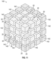
- FIG. 11 is a schematic of an exemplary embodiment of a cube-shaped monolithic multi-dimensional memory architecture in accordance with the present disclosure
- FIG. 12 is a schematic of an exemplary embodiment of a monolithic multi-dimensional memory architecture incorporated into an exemplary monolithic multi-dimensional integrated circuit in accordance with the present disclosure
- FIG. 13 is a perspective view of a honeycomb-shaped monolithic multi-dimensional memory architecture in accordance with the present disclosure
- FIG. 14 is a schematic of an exemplary embodiment of a monolithic multi-dimensional integrated circuit in accordance with the present disclosure.
- FIG. 15 is a schematic of an exemplary embodiment of a monolithic multi-dimensional integrated circuit with solar cells in accordance with the present disclosure
- FIG. 16 is a schematic of exemplary embodiments of semiconductor wafers with solar cells on multi-dimensional surfaces in accordance with the present disclosure
- FIG. 17 is a schematic of exemplary embodiments of semiconductor wafers with solar cells on multi-dimensional surfaces in accordance with the present disclosure
- FIG. 18 is schematic of exemplary embodiments of multi-dimensional die and on-chip solar microcells structure in accordance with the present disclosure
- FIG. 19 is a perspective view of a photonic integrated circuit in accordance with the present disclosure.
- FIG. 20 is a perspective view of a photonic integrated circuit in accordance with the present disclosure.
- FIG. 21 is a perspective view of a photonic integrated circuit in accordance with the present disclosure.
- FIG. 22 is a front view of a photonic integrated circuit in accordance with the present disclosure.
- FIG. 23 is a perspective and detail view of a multi-dimensional photonic integrated circuit in accordance with the present disclosure.
- FIG. 24 is a perspective and detail view of a multi-dimensional photonic integrated circuit in accordance with the present disclosure.
- FIG. 25 is a perspective and detail view of a multi-dimensional photonic integrated circuit in accordance with the present disclosure.
- FIG. 27 is a perspective and detail view of a multi-dimensional photonic integrated circuit with on-chip solar cells in accordance with the present disclosure
- FIG. 29 is a perspective view of a monolithic multi-dimensional memory architecture incorporated into a multi-dimensional photonic integrated circuit in accordance with the present disclosure
- FIG. 30 is a perspective view of a monolithic multi-dimensional memory architecture incorporated into a multi-dimensional photonic integrated circuit in accordance with the present disclosure
- FIG. 31 is a perspective view of a monolithic multi-dimensional memory architecture incorporated into a multi-dimensional photonic integrated circuit in accordance with the present disclosure
- FIG. 32 is a perspective view of a hybrid system of multi-dimensional integrated circuits and multi-dimensional photonic integrated circuits in accordance with the present disclosure
- FIG. 33 is a diagram showing communication between multi-dimensional integrated circuits and multi-dimensional photonic integrated circuits in accordance with the present disclosure.
- FIG. 34 is a perspective view of a multi-dimensional photonic integrated circuit being fabricated in accordance with the present disclosure.
- exemplary embodiments of monolithic multi-dimensional integrated circuits will first be described.
- Exemplary ICs are built on both sides of an electronic board and have a multi-dimensional integration utilizing all if the IC package's planes for semiconductor circuitry.
- the IC architecture may be comprised of wafers located on any and all planes of a rectangular or square package for maximum area utilization. This type of structure enables multi-dimensional utilization of integrated circuits for all manufacturing processes.
- An exemplary monolithic multi-dimensional integrated circuit 10 comprises an electronic board 12 and one or more semiconductor wafers 14 .
- the semiconductor wafers 14 may be any shape or may be of several different shapes. As discussed in more detail herein, in exemplary embodiments the multiple planes or the wafers have a honeycomb or beehive shape.
- the electronic board 12 has two opposite sides 16 a , 16 b , and IC 10 and wafers 14 are mounted on both sides 16 a , 16 b of the board 12 .
- FIG. 1 shows a multi-dimensional integrated circuit cross-section mounted on electronic board. The multi-dimensional integrated circuit is located on both sides of an electronic board.
- the semiconductor wafers 14 may be mounted on one or more of the planes 20 of the electronic package 18 and may be mounted on all its planes.
- multiple ICs are constructed on one or more planes of the electronic package 18 .
- a multi-dimensional electronic package 18 is provided and is comprised of multiple planes 20 a - 20 d , best seen in FIG. 4 .
- any type of circuit could be placed on any plane of the multi-dimensional integrated circuit.
- This electronic circuitry could be designed hierarchically in layers.
- a plurality of layered integrated circuits could be placed on a single semiconductor wafer.
- a multi-dimensional integrated circuit 10 may contain semiconductor wafers 14 on multiple sides or on all sides.
- FIG. 3 demonstrates different wafer sizes.
- an exemplary multi-dimensional IC 10 is comprised of a plurality of tiers or planes utilized for the electronic circuitry area, where the IC layout is designed to be electronically connected taking multi-dimensional planes into consideration.
- Each tier or plane may have electronic circuits, and a plurality of monolithic multi-dimensional wafers and circuits could be located on all planes, enabling efficient silicon area for maximum utilization.
- An internal, silicon based, heat-sink mechanism may provide advanced temperature control for the entire integrated circuit.
- FIG. 4 shows the inner horizontal and vertical connectivity.
- Multi-directional crossbars 26 may be associated with a first tier of a plurality of tiers or planes.
- the multi-directional crossbars 26 couple a plurality of electronic circuitry units within a single tier to vertical crossbars 24 .
- the crossbars may be centrally located in between the planes according to connectivity necessities.
- the multi-directional crossbars 26 support a shuffle architecture.
- the ICs may be connected to IO pads via internal metal wires that are routed in multi-dimensional planes.
- the IC structure may include interconnects die side-side wire bars to connect between the silicon's internal connections and the IO PADs.
- the multi-dimensional electronic circuitry has crossed over power supplies to provide power to all integrated circuits on the wafer, in all planes.
- FIG. 2 shows connected VIAs 24 running vertically from top to bottom.
- the internal connections described may support an in/out architecture.
- Metal crossbars 22 , 24 , 26 may cross side-to-side and top-down in order to perform the electronic connections that are necessary for the IC's circuitry.
- the multi-dimensional layout structure typically comprises vertical and horizontal connectivity on the order of microns long.
- at least one horizontal crossbar 22 communicates signals within a horizontal plane 20 .
- a horizontal crossbar 22 may be provided for power supplies within a first tier or horizontal plane.
- One or more vertical crossbars 24 may be provided to provide communication between electronic circuitry units. As best seen in FIG.
- one or more multi-directional crossbars 26 communicate signals between one or more electronic circuitry units in a single plane to at least one vertical crossbar 24 .
- at least one tier or plane comprises all-directions signals routings.
- each electronic circuitry unit is connected to the second tier that may be on any plane of the package, but the circuitry could be connected to any tier on any plane.
- the integrated circuits are connected via multi-dimensional VIAs at all planes' levels.
- These “through-silicon VIAs” (TSVs) pass through the silicon substrate(s) between active layers and/or between an active layer and an external bond pad.
- TSVs through-silicon VIAs
- the large numbers of vertical VIAs between the layers advantageously allows construction of wide bandwidth routing buses between functional blocks in different layers.
- a typical example would be a microcontroller and memory multi-dimensional stack, with the cache memory stacked on top of the processor. This arrangement allows a bus much wider than the typical 128 or 256 bits between the cache and microcontroller. Wide buses in turn alleviate the memory wall problem.
- An exemplary method of forming a multi-dimensional circuitry structure in an IC includes positioning a first electronic circuit unit on a first tier or plane of a multi-dimensional IC and positioning a second electronic circuitry unit on a second tier or plane of the multi-dimensional IC.
- Third, fourth, and additional electronic circuitry units could be positioned on respective tiers or planes of the IC.
- the first electronic circuitry unit may be coupled to the second electronic circuitry unit with vertical crossbars.
- one or more multi-directional crossbars are provided within one of the electronic circuit's units at all planes.
- Control logic may be provided and configured to determine which, if any, electronic circuits within the first and second electronic circuit units are active and to reconfigure usage of the units based on such determination by deactivating those units that are not active.
- the manufacturing of the multi-dimensional IC may be done utilizing Die-to-Die, Die-to-Wafer or Wafer-to-Water methods, depending on the needs and goals of the manufacturer and based on the knowledge of the skilled artisan.
- Each manufacturing methodology has its advantages and disadvantages according to the design process and node's size.
- the electronic components are built on multiple dies, which are then aligned and bonded. Thinning and TSV creation may be done before or after bonding.
- One advantage of die-to-die is that each component die can be tested first, so that one bad die does not ruin an entire stack.
- each die in the 3D IC can be binned beforehand, so that they can be mixed and matched to optimize power consumption and performance (e.g., matching multiple dice from the low power process corner for a mobile application).
- the electronic components are built on two or more semiconductor wafers, which are then aligned, bonded, and diced into the multi-dimensional ICs.
- Each wafer may be thinned before or after bonding.
- Vertical connections are either built into the wafers before bonding or created in the stack after bonding.
- TSVs through-silicon VIAs
- Wafer-to-wafer bonding can reduce yields, since if any 1 of N chips in a multi-dimensional IC are defective, the entire 3D IC will be defective.
- the wafers must be the same size, but many exotic materials (e.g.
- III-Vs are manufactured on much smaller wafers than CMOS logic or DRAM (typically 300 mm and below), complicating heterogeneous integration.
- the sub-wafer's layers can be built with different processes, or even on different types of wafers. This means that components can be optimized to a much greater degree than if they were built together on a single wafer. Moreover, components with incompatible manufacturing could be combined in a single multi-dimensional IC.
- Monolithic multi-dimensional memory architecture 110 generally is comprised of a multi-dimensional, multiple plane memory crossbar architecture with tight-pitched vertical, horizontal and angled monolithic inter-tier vias (MIVs) 114 for inter-unit routing and multiplexers at each tier for block access are used to shorten overall conductor length and reduce resistive-capacitive (RC) delay. More particularly, exemplary embodiments have one or more tiers or planes 112 and monolithic inter-tier vias 114 spanning the tiers.
- MIVs monolithic inter-tier vias
- memory cells may be placed on a honeycomb structure. Silicon sub-dies can be placed on all honeycomb planes and connected via crossbars or other electrical conductors.
- At least one tier memory unit may lie in planes perpendicular to the other memory units and/or in planes parallel to the other memory units and/or in planes at any angle to the other memory units.
- a basic structure would have at least one horizontal crossbar for memory cells 116 within tiers 112 .
- a stack of memory integrated circuit memory chips are located on multi-planar structure and connected via vertical, horizontal and angled crossbars.
- the memory cells 116 may have random access memory (RAM), and the RAM may comprise static RAM (SRAM).
- RAM random access memory
- SRAM static RAM
- one or more of the memory cells 116 could have a three-dimensional mask-programmed read-only memory (3D-MPROM) or a three-dimensional electrically-programmable read-only memory (3D-EPROM).
- FIGS. 6 - 8 illustrate multi-planar structures for memory cells allocation.
- FIG. 6 shows one plane within a honeycomb structure 125 .
- FIG. 7 shows an exemplary structure comprised of multiple planes 112 and monolithic inter-tier vias 114 spanning the planes 112 . Silicon sub-dies may be glued/mounted to these planes enabling significantly higher surface area for memory cells allocation.
- FIG. 8 Another planar structure for memory cells allocations is shown in FIG. 8 , also having multiple planes 112 and monolithic inter-tier vias 114 spanning the planes 112 . Silicon sub-dies are glued/mounted on each plane, significantly enhancing the surface area for memory cells allocation.
- the honeycomb/bee hive structure illustrated in FIGS. 9 and 10 advantageously enables shorter, more efficient MIV structure.
- Silicon sub-dies can be placed on the honeycomb planes.
- Implementation of this type of structural design for memory silicon dies significantly increases the surface area for memory cells implementation.
- the multi-plane, multi-dimensional memory layout surface design advantageously enables significantly larger capacity to implement more memory cells on the same area than current industry standard structures.
- a multiplexer 118 is disposed in one of the tiers or in multiple tiers.
- the multiplexer 118 is communicatively coupled to the memory cell 116 in the respective tier 112 .
- a second multiplexer 118 a is disposed in a second tier or plane among a plurality of tiers and coupled to a second respective memory cell 116 a within the second tier.
- Control logic 120 may be used to configure the memory banks based on use. More particularly, control logic may be used to determine whether the memory cells 116 are active and which memory cells 116 are active and to control usage of the memory cells 116 based on such determinations. In exemplary embodiments, the control logic is configured to reconfigure usage of memory cells deactivates unused memory cells so that power is conserved.
- the stack of memory units is located on multiple planes in multiple dimensions.
- a series of memory units may be arranged in a bee hive or honeycomb structure and connected via vertical, horizontal or angled crossbars, creating a memory structure having multiple planes in multiple dimensions.
- the series of memory units may be held together by glue or another adhesive to make one memory microchip.
- the IC may be comprised of silicon sub-dies of memory cells, each glued/mounted on a different plane and connected via crossbars or any other electrical conductor.
- the silicon sub-dies may be on different planes and can be on different manufacturing process nodes and connected via crossbars or any other electrical conductor.
- the series of memory units is structurally integrated to a microprocessor chip to constitute a microprocessor and a memory module.
- a first step is positioning a first client memory unit 117 a on a first plane 112 a of a multi-dimensional memory integrated circuit 10 .
- a second client memory unit 117 b is positioned on a second plane 112 b of the multi-dimensional memory integrated circuit.
- At least one vertical, horizontal or angled crossbar 22 , 24 , 26 , 114 may be provided within one of the client memory units 117 .
- Subsequent steps include coupling the first client memory unit 117 a to the second client memory unit 117 b with a vertical, horizontal or angled crossbar 22 , 24 , 26 , 114 and providing control logic 120 .
- the control logic 120 is configured to determine which, if any, memory cells 116 within the first and second client memory units 117 are active and reconfigure usage of the client memory units 117 based on such determination by deactivating client memory units which are not active.
- dies are used in manufacturing disclosed multi-dimensional ICs and packages, and the multi-dimensional die and said intermediate-circuit dies may be located in a memory package, a memory module, a memory card or a solid-state drive.
- FIGS. 14 - 18 monolithic multi-dimensional integrated circuits incorporating solar cells will now be described.
- solar cells and/or MEMS can be mounted on or incorporated into the multiple-planes wafers described above for purposes of charging various devices.
- the solar cells can be produced as MEMS or on-chip solar cells based on nanotechnology research and development.
- FIG. 14 illustrates an exemplary multi-dimensional integrated circuit having multiple planes 20 suitable for on-chip solar cells.
- wafers 14 of the integrated circuit 10 may include solar cells 28 . More particularly, the semiconductor wafers 14 may be mounted on all planes 20 of the electronic package 18 and comprise non-silicon substrate on-chip solar cells 28 . As best seen in FIGS. 16 and 17 , in exemplary embodiments the semiconductor wafers 14 are mounted on selected planes 20 of the multi-dimensional structure and comprise silicon on-chip solar cells 28 . FIG. 18 shows a multi-dimensional die and on-chip solar microcells structure. The semiconductor wafers could be mounted on all planes of the electronic package and comprise silicon MEMS and/or on-chip solar cells structure. The solar cells may be fully integrated within the integrated circuit structure for power harvesting. In exemplary embodiments, photo diodes, electrically connected, are used as on-chip micro solar cells.
- a photonic integrated circuit (PIC) 209 is a chip that contains photonic or optical components 215 , i.e., components that work with light (photons). Whereas conventional integrated circuits work by conducting electricity or allowing electrons to flow through the circuit, PICs utilize photons, massless fundamental particles representing a quantum of light, instead of electrons. In a photonic chip, photons pass through optical components such as waveguides (equivalent to electrical wires), lasers (equivalent to transistors), and similar.
- PICs typically use a laser source to inject light that drives the components, like turning on/off a typical electron-based CMOS transistor.
- CMOS transistor electrons are injected to drive electronic components as in PICs light is used instead of electrons.
- Photonic integrated circuits are typically fabricated with a wafer-scale technology using lithography on silicon related materials substrates.
- An exemplary multi-dimensional photonic integrated circuit (MD PIC) 210 is comprised of a photonic integrated circuit 209 including a substrate 212 having two sides 216 a , 216 b and a multi-dimensional package 218 with planes 220 that extend in multiple dimensions.
- the planes 220 may have horizontal sides 213 a and vertical sides 213 b .
- Optical components 215 such as waveguides or lasers are mounted on or otherwise connected to one or both sides 216 a , 216 b of the package 218 as well as being mounted on the package's multi-dimensional planes 220 on the horizontal 213 a and/or vertical sides 213 b .
- At least one of the optical components 215 is mounted on at least one of the horizontal sides 213 a
- another optical component 215 is mounted on at least one of the vertical sides 213 b
- the optical components 215 may be mounted on all the planes 220 of the package 218 .
- the optical components 215 of a PIC 209 include a laser 215 a and one or more optical waveguides 215 b .
- a laser injects light into the PIC 209 to drive the other optical components 215 , and the waveguides guide the light, restricting the spatial region where the photons can propagate. This enables the PIC 209 to operate using the photons of light.
- the optical components 215 may be connected by optical fiber 217 that runs throughout the PIC 209 .
- the multi-dimensional planes 220 of the package 218 can be of various structures such as hexahedron, dodecahedron, icosahedron, and can have a honeycomb/beehive structure 219 .
- the optical components 215 can be placed on the honeycomb planes. Implementation of this type of structural design significantly increases the surface area for memory cells implementation.
- the multi-planar, multi-dimensional memory layout surface design advantageously enables significantly larger capacity to implement more memory cells on the same area.
- exemplary multi-dimensional photonic integrated circuits 210 incorporate solar cells.
- On-chip solar cells and/or MEMS can be mounted on or incorporated into the multiple-planes described above.
- the solar cells 228 may be mounted on all planes 220 of the package 218 and comprise silicon or non-silicon substrate on-chip solar cells.
- the solar cells 228 may be fully integrated within the photonic circuit structure for power harvesting.
- the multi-dimensional photonic integrated circuit 210 can include multi-dimensional memory architecture 310 , which is comprised of a multi-dimensional, multiple plane memory crossbar architecture with tight-pitched vertical, horizontal, and angled monolithic inter-tier vias (MIVs) 314 for inter-unit routing. There may be multiplexers at each tier for block access used to shorten overall conductor length and reduce resistive-capacitive (RC) delay. Exemplary embodiments have one or more tiers or planes 312 and monolithic inter-tier vias 314 spanning the tiers.
- each tier or plane 312 there is at least one memory cell 316 in each tier or plane 312 and the memory cell 316 may be located within a client memory unit. At least one tier memory unit may lie in planes perpendicular to the other memory units and/or in planes parallel to the other memory units and/or in planes at any angle to the other memory units.
- a basic structure would have at least one horizontal crossbar for memory cells 316 within tiers 312 .
- the memory cells 316 may have random access memory (RAM), and the RAM may comprise static RAM (SRAM).
- one or more of the memory cells 316 could have a three-dimensional mask-programmed read-only memory (3D-MPROM) or a three-dimensional electrically-programmable read-only memory (3D-EPROM).
- a hybrid system 202 of conventional multi-dimensional integrated circuits 10 and multi-dimensional photonic integrated circuits 210 is provided.
- the multi-dimensional integrated circuit 10 communicates with the multi-dimensional photonic integrated circuit 210 by electrical communication and/or photonic communication.
- the conventional 3D, MP circuitries/chip 10 communicates with the photonic circuitries/chip 210 via optical based wiring connections.
- microfiber optics may function as light-based-wires.
- Another option is light conducting wires that are like fiber optics in structure but embedded into the silicon substrate. It should be noted that any type of light conducting material that functions as wire and can be implemented within a microchip could be used.
- the signals are transmitted using a light source such as a laser 215 a , high intensity LEDs, or any other similar light source.
- a light source such as a laser 215 a , high intensity LEDs, or any other similar light source.
- fiber optics or any other light oriented medium that is functioning as wire can be bent according to the 3D, MP shape and enable electrical connectivity. These and other modifications could be done during fabrication of a multi-dimension PIC, a stage of which is shown in FIG. 34 .
- Dedicated circuitries are made to produce the light-based communication between circuits and can transmit the signals in different frequencies. This feature enables multiplexing capabilities, meaning transmitting different data on the same light wire as a frequency dependent. For example, on one light-based wire using one frequency specific data can be transmitted and using different frequency will transmit another data.
- the light pulses can alternate and transmit many data to many circuitries or components on the same line, very similar to transmitting data signals over high power lines for example.
- multi-dimensional integrated circuit 10 comprises an electronic board 12 and one or more semiconductor wafers 14 .
- the electronic board 12 has two opposite sides 16 a , 16 b , and IC 10 and wafers 14 are mounted on both sides 16 a , 16 b of the board 12 .
- the semiconductor wafers 14 may be mounted on one or more of the planes 20 of the electronic package 18 and may be mounted on all its planes.
- multiple ICs are constructed on one or more planes of the electronic package 18 .
- a multi-dimensional electronic package 18 is provided and is comprised of multiple planes 20 a - 20 d .
- multi-dimensional PIC 210 has a substrate 212 with two sides 216 a , 216 b and a multi-dimensional package 218 with planes 220 that extend in multiple dimensions.
- Optical components 215 are mounted on one or both sides 216 a , 216 b of the package 218 as well as being mounted on the package's multi-dimensional planes 220 .
- a hybrid system is advantageous for many applications, including in the telecommunications industry where high-speed information is transmitted along fiber optic waveguides.
- the information must ultimately be converted into digital signals for common electronic devices to process since common data networks and power infrastructures exist on electrical structures and not photonic ones.
- PICs will likely continue replacing conventional ICs within a wide range of applications.
- Disclosed embodiments include and enable larger PICs, with higher performance and less energy/heat loss. These chips increase the traffic speed and bandwidth of data centers, reduce power consumption/heat, lowering cost, and ultimately helping create a “greener world”. Embodiments of the present disclosure encapsulate the next generation of high performance, bandwidth, and efficiency of PICs, making them a vital part of the high-speed technology of the future.
Landscapes
- Engineering & Computer Science (AREA)
- Physics & Mathematics (AREA)
- General Physics & Mathematics (AREA)
- Power Engineering (AREA)
- Microelectronics & Electronic Packaging (AREA)
- Condensed Matter Physics & Semiconductors (AREA)
- Computer Hardware Design (AREA)
- Life Sciences & Earth Sciences (AREA)
- Sustainable Development (AREA)
- Health & Medical Sciences (AREA)
- Molecular Biology (AREA)
- Ceramic Engineering (AREA)
- Manufacturing & Machinery (AREA)
- Sustainable Energy (AREA)
- Optics & Photonics (AREA)
- Semiconductor Integrated Circuits (AREA)
Abstract
Description
Claims (21)
Priority Applications (1)
| Application Number | Priority Date | Filing Date | Title |
|---|---|---|---|
| US18/109,291 US11862736B2 (en) | 2018-09-17 | 2023-02-14 | Multi-dimensional photonic integrated circuits and memory structure having optical components mounted on multiple planes of a multi-dimensional package |
Applications Claiming Priority (6)
| Application Number | Priority Date | Filing Date | Title |
|---|---|---|---|
| US201862732023P | 2018-09-17 | 2018-09-17 | |
| US201862732026P | 2018-09-17 | 2018-09-17 | |
| US16/292,388 US10854763B2 (en) | 2018-09-17 | 2019-03-05 | Multi-dimensional integrated circuit having multiple planes and memory architecture having a honeycomb or bee hive structure |
| US17/102,928 US11411127B2 (en) | 2018-09-17 | 2020-11-24 | Multi-dimensional integrated circuits having semiconductors mounted on multi-dimensional planes and multi-dimensional memory structure |
| US17/876,981 US12199196B2 (en) | 2018-09-17 | 2022-07-29 | Multi-dimensional integrated circuits having semiconductors mounted on multi- dimensional planes and multi-dimensional memory structure |
| US18/109,291 US11862736B2 (en) | 2018-09-17 | 2023-02-14 | Multi-dimensional photonic integrated circuits and memory structure having optical components mounted on multiple planes of a multi-dimensional package |
Related Parent Applications (1)
| Application Number | Title | Priority Date | Filing Date |
|---|---|---|---|
| US17/876,981 Continuation-In-Part US12199196B2 (en) | 2018-09-17 | 2022-07-29 | Multi-dimensional integrated circuits having semiconductors mounted on multi- dimensional planes and multi-dimensional memory structure |
Publications (2)
| Publication Number | Publication Date |
|---|---|
| US20230207711A1 US20230207711A1 (en) | 2023-06-29 |
| US11862736B2 true US11862736B2 (en) | 2024-01-02 |
Family
ID=86897330
Family Applications (1)
| Application Number | Title | Priority Date | Filing Date |
|---|---|---|---|
| US18/109,291 Active US11862736B2 (en) | 2018-09-17 | 2023-02-14 | Multi-dimensional photonic integrated circuits and memory structure having optical components mounted on multiple planes of a multi-dimensional package |
Country Status (1)
| Country | Link |
|---|---|
| US (1) | US11862736B2 (en) |
Citations (24)
| Publication number | Priority date | Publication date | Assignee | Title |
|---|---|---|---|---|
| US4603374A (en) | 1984-07-03 | 1986-07-29 | Motorola, Inc. | Packaging module for a semiconductor wafer |
| US5817543A (en) | 1993-11-03 | 1998-10-06 | International Business Machines Corporation | Method of constructing an integrated circuit memory |
| US6033931A (en) | 1997-08-18 | 2000-03-07 | Texas Instruments Incorporated | Semiconductor device including stacked chips having metal patterned on circuit surface and one edge side of chip |
| US6054757A (en) | 1997-02-27 | 2000-04-25 | Oki Electric Industry Co., Ltd. | Semiconductor apparatus, circuit board and combination thereof |
| US20040104469A1 (en) | 2000-10-02 | 2004-06-03 | Yoshihiko Yagi | Card type recording medium and production method therefor |
| US20040108590A1 (en) | 2000-10-16 | 2004-06-10 | Kledzik Kenneth J. | Carrier-based electronic module |
| US20040178514A1 (en) | 2003-03-12 | 2004-09-16 | Lee Sang-Hyeop | Method of encapsulating semiconductor devices on a printed circuit board, and a printed circuit board for use in the method |
| US20070023887A1 (en) | 2005-07-29 | 2007-02-01 | Nec Electronics Corporation | Multi-chip semiconductor package featuring wiring chip incorporated therein, and method for manufacturing such multi-chip semiconductor package |
| US7537966B2 (en) | 2002-07-10 | 2009-05-26 | Micron Technology, Inc. | Method for fabricating board on chip (BOC) semiconductor package with circuit side polymer layer |
| US20100304521A1 (en) * | 2006-10-09 | 2010-12-02 | Solexel, Inc. | Shadow Mask Methods For Manufacturing Three-Dimensional Thin-Film Solar Cells |
| US20120138997A1 (en) * | 2009-06-26 | 2012-06-07 | Asahi Rubber Inc. | White color reflecting material and process for production thereof |
| US20120248595A1 (en) | 2010-11-18 | 2012-10-04 | MonolithlC 3D Inc. | System comprising a semiconductor device and structure |
| US8299592B2 (en) | 2009-01-23 | 2012-10-30 | Hynix Semiconductor Inc. | Cube semiconductor package composed of a plurality of stacked together and interconnected semiconductor chip modules |
| US8673686B2 (en) | 2011-06-09 | 2014-03-18 | Hung-Jen LEE | Chip package structure and manufacturing method thereof |
| US20140111269A1 (en) | 2012-10-24 | 2014-04-24 | National Changhua University Of Education | Through-silicon via self-routing circuit and routing method thereof |
| US20140293531A1 (en) * | 2013-03-27 | 2014-10-02 | Hewlett-Packard Development Company, L.P. | Server node |
| US20150123284A1 (en) | 2013-11-07 | 2015-05-07 | Chajea JO | Semiconductor devices having through-electrodes and methods for fabricating the same |
| US20150282294A1 (en) | 2014-03-31 | 2015-10-01 | Panasonic Intellectual Property Management Co., Ltd. | Elastic flexible substrate and manufacturing method thereof |
| US9379091B2 (en) | 2011-07-27 | 2016-06-28 | Micron Technology, Inc. | Semiconductor die assemblies and semiconductor devices including same |
| US20160197235A1 (en) * | 2013-09-02 | 2016-07-07 | Lg Innotek Co., Ltd. | Light-emitting element |
| US20180053544A1 (en) | 2015-03-10 | 2018-02-22 | Rambus Inc. | Memories and memory components with interconnected and redundant data interfaces |
| US20180096872A1 (en) | 2015-07-14 | 2018-04-05 | Taiwan Semiconductor Manufacturing Co., Ltd. | 3d ic bump height metrology apc |
| US20190122960A1 (en) | 2013-11-12 | 2019-04-25 | Taiwan Semiconductor Manufacturing Co., Ltd. | Apparatus and method of three dimensional conductive lines |
| US10854763B2 (en) | 2018-09-17 | 2020-12-01 | Gbt Technologies Inc. | Multi-dimensional integrated circuit having multiple planes and memory architecture having a honeycomb or bee hive structure |
-
2023
- 2023-02-14 US US18/109,291 patent/US11862736B2/en active Active
Patent Citations (25)
| Publication number | Priority date | Publication date | Assignee | Title |
|---|---|---|---|---|
| US4603374A (en) | 1984-07-03 | 1986-07-29 | Motorola, Inc. | Packaging module for a semiconductor wafer |
| US5817543A (en) | 1993-11-03 | 1998-10-06 | International Business Machines Corporation | Method of constructing an integrated circuit memory |
| US6054757A (en) | 1997-02-27 | 2000-04-25 | Oki Electric Industry Co., Ltd. | Semiconductor apparatus, circuit board and combination thereof |
| US6033931A (en) | 1997-08-18 | 2000-03-07 | Texas Instruments Incorporated | Semiconductor device including stacked chips having metal patterned on circuit surface and one edge side of chip |
| US20040104469A1 (en) | 2000-10-02 | 2004-06-03 | Yoshihiko Yagi | Card type recording medium and production method therefor |
| US20040108590A1 (en) | 2000-10-16 | 2004-06-10 | Kledzik Kenneth J. | Carrier-based electronic module |
| US7537966B2 (en) | 2002-07-10 | 2009-05-26 | Micron Technology, Inc. | Method for fabricating board on chip (BOC) semiconductor package with circuit side polymer layer |
| US20040178514A1 (en) | 2003-03-12 | 2004-09-16 | Lee Sang-Hyeop | Method of encapsulating semiconductor devices on a printed circuit board, and a printed circuit board for use in the method |
| US20070023887A1 (en) | 2005-07-29 | 2007-02-01 | Nec Electronics Corporation | Multi-chip semiconductor package featuring wiring chip incorporated therein, and method for manufacturing such multi-chip semiconductor package |
| US20100304521A1 (en) * | 2006-10-09 | 2010-12-02 | Solexel, Inc. | Shadow Mask Methods For Manufacturing Three-Dimensional Thin-Film Solar Cells |
| US8299592B2 (en) | 2009-01-23 | 2012-10-30 | Hynix Semiconductor Inc. | Cube semiconductor package composed of a plurality of stacked together and interconnected semiconductor chip modules |
| US20120138997A1 (en) * | 2009-06-26 | 2012-06-07 | Asahi Rubber Inc. | White color reflecting material and process for production thereof |
| US20120248595A1 (en) | 2010-11-18 | 2012-10-04 | MonolithlC 3D Inc. | System comprising a semiconductor device and structure |
| US8673686B2 (en) | 2011-06-09 | 2014-03-18 | Hung-Jen LEE | Chip package structure and manufacturing method thereof |
| US9379091B2 (en) | 2011-07-27 | 2016-06-28 | Micron Technology, Inc. | Semiconductor die assemblies and semiconductor devices including same |
| US20140111269A1 (en) | 2012-10-24 | 2014-04-24 | National Changhua University Of Education | Through-silicon via self-routing circuit and routing method thereof |
| US20140293531A1 (en) * | 2013-03-27 | 2014-10-02 | Hewlett-Packard Development Company, L.P. | Server node |
| US20160197235A1 (en) * | 2013-09-02 | 2016-07-07 | Lg Innotek Co., Ltd. | Light-emitting element |
| US20150123284A1 (en) | 2013-11-07 | 2015-05-07 | Chajea JO | Semiconductor devices having through-electrodes and methods for fabricating the same |
| US20190122960A1 (en) | 2013-11-12 | 2019-04-25 | Taiwan Semiconductor Manufacturing Co., Ltd. | Apparatus and method of three dimensional conductive lines |
| US20150282294A1 (en) | 2014-03-31 | 2015-10-01 | Panasonic Intellectual Property Management Co., Ltd. | Elastic flexible substrate and manufacturing method thereof |
| US20180053544A1 (en) | 2015-03-10 | 2018-02-22 | Rambus Inc. | Memories and memory components with interconnected and redundant data interfaces |
| US20180096872A1 (en) | 2015-07-14 | 2018-04-05 | Taiwan Semiconductor Manufacturing Co., Ltd. | 3d ic bump height metrology apc |
| US10854763B2 (en) | 2018-09-17 | 2020-12-01 | Gbt Technologies Inc. | Multi-dimensional integrated circuit having multiple planes and memory architecture having a honeycomb or bee hive structure |
| US11411127B2 (en) * | 2018-09-17 | 2022-08-09 | Gbt Technologies Inc. | Multi-dimensional integrated circuits having semiconductors mounted on multi-dimensional planes and multi-dimensional memory structure |
Non-Patent Citations (2)
| Title |
|---|
| International Search Report and Written Opinion dated Jan. 9, 2020 in related International Application No. PCT/US2019/050266. |
| Partial Supplementary European Search Report dated Sep. 2, 2022 in related European Patent Application No. 19862631.9. |
Also Published As
| Publication number | Publication date |
|---|---|
| US20230207711A1 (en) | 2023-06-29 |
Similar Documents
| Publication | Publication Date | Title |
|---|---|---|
| JP7542049B2 (en) | Semiconductor Devices | |
| US12199196B2 (en) | Multi-dimensional integrated circuits having semiconductors mounted on multi- dimensional planes and multi-dimensional memory structure | |
| CN111727503B (en) | Unified semiconductor device with programmable logic device and heterogeneous memory and method of forming the same | |
| KR102780323B1 (en) | Compact 3D stacked CFET architecture for complex logic cells | |
| US11600586B2 (en) | 3D semiconductor devices and structures with electronic circuit units | |
| US11270988B2 (en) | 3D semiconductor device(s) and structure(s) with electronic control units | |
| CN101295693B (en) | Semiconductor device | |
| US11800725B1 (en) | 3D semiconductor devices and structures with electronic circuit units | |
| US11488939B2 (en) | 3D semiconductor devices and structures with at least one vertical bus | |
| CN116960002B (en) | Optoelectronic integrated semiconductor packaging structure and preparation method thereof | |
| US11862736B2 (en) | Multi-dimensional photonic integrated circuits and memory structure having optical components mounted on multiple planes of a multi-dimensional package | |
| US12433031B2 (en) | 3D semiconductor devices and structures with electronic circuit units | |
| US12021028B2 (en) | 3D semiconductor devices and structures with electronic circuit units | |
| CN119694998A (en) | Packaging structure and packaging method | |
| CN108595748B (en) | Three-dimensional topological structure of antifuse Field Programmable Gate Array (FPGA) | |
| US20260006803A1 (en) | Methods of manufacturing 3d semiconductor devices and structures with electronic circuit units | |
| US20260040586A1 (en) | 3d semiconductor devices and structures with functional units and pillars | |
| US20230413586A1 (en) | 3d semiconductor devices and structures with electronic circuit units | |
| CN119291861A (en) | An optoelectronic co-packaging structure based on embedded active silicon bridge | |
| CN120674414A (en) | Integrated circuit assembly | |
| CN115643791A (en) | A system integrated single chip, generation method and readable storage medium | |
| CN121463556A (en) | An optoelectronic integrated semiconductor packaging structure and its fabrication method | |
| CN105990352A (en) | Separated three-dimensional vertical memory | |
| CN105990351A (en) | Separated 3D longitudinal memory |
Legal Events
| Date | Code | Title | Description |
|---|---|---|---|
| FEPP | Fee payment procedure |
Free format text: ENTITY STATUS SET TO UNDISCOUNTED (ORIGINAL EVENT CODE: BIG.); ENTITY STATUS OF PATENT OWNER: SMALL ENTITY |
|
| FEPP | Fee payment procedure |
Free format text: ENTITY STATUS SET TO SMALL (ORIGINAL EVENT CODE: SMAL); ENTITY STATUS OF PATENT OWNER: SMALL ENTITY |
|
| STPP | Information on status: patent application and granting procedure in general |
Free format text: NOTICE OF ALLOWANCE MAILED -- APPLICATION RECEIVED IN OFFICE OF PUBLICATIONS |
|
| AS | Assignment |
Owner name: GOPHER PROTOCOL, INC., CALIFORNIA Free format text: ASSIGNMENT OF ASSIGNORS INTEREST;ASSIGNORS:RITTMAN, DAN;SCHNAPP, ALIZA;SIGNING DATES FROM 20181205 TO 20181206;REEL/FRAME:064535/0556 Owner name: GBT TECHNOLOGIES INC., CALIFORNIA Free format text: MERGER AND CHANGE OF NAME;ASSIGNORS:GOPHER PROTOCOL INC.;GBT TECHNOLOGIES INC.;REEL/FRAME:065518/0058 Effective date: 20200207 |
|
| AS | Assignment |
Owner name: GBT TOKENIZE CORP., CALIFORNIA Free format text: ASSIGNMENT OF ASSIGNORS INTEREST;ASSIGNOR:GBT TECHNOLOGIES INC.;REEL/FRAME:065420/0434 Effective date: 20230807 Owner name: GBT TOKENIZE CORP., CALIFORNIA Free format text: ASSIGNMENT OF ASSIGNOR'S INTEREST;ASSIGNOR:GBT TECHNOLOGIES INC.;REEL/FRAME:065420/0434 Effective date: 20230807 |
|
| STCB | Information on status: application discontinuation |
Free format text: ABANDONED -- FAILURE TO PAY ISSUE FEE |
|
| STPP | Information on status: patent application and granting procedure in general |
Free format text: PUBLICATIONS -- ISSUE FEE PAYMENT RECEIVED |
|
| FEPP | Fee payment procedure |
Free format text: PETITION RELATED TO MAINTENANCE FEES GRANTED (ORIGINAL EVENT CODE: PTGR); ENTITY STATUS OF PATENT OWNER: SMALL ENTITY |
|
| STPP | Information on status: patent application and granting procedure in general |
Free format text: PUBLICATIONS -- ISSUE FEE PAYMENT VERIFIED |
|
| STCF | Information on status: patent grant |
Free format text: PATENTED CASE |